US5706952A - Continuous carrier for electrical or mechanical components - Google Patents
Continuous carrier for electrical or mechanical componentsDownload PDFInfo
- Publication number
- US5706952A US5706952AUS08/584,534US58453496AUS5706952AUS 5706952 AUS5706952 AUS 5706952AUS 58453496 AUS58453496 AUS 58453496AUS 5706952 AUS5706952 AUS 5706952A
- Authority
- US
- United States
- Prior art keywords
- components
- strip
- filament
- strips
- continuous carrier
- Prior art date
- Legal status (The legal status is an assumption and is not a legal conclusion. Google has not performed a legal analysis and makes no representation as to the accuracy of the status listed.)
- Expired - Lifetime
Links
- 239000004033plasticSubstances0.000claimsabstractdescription45
- 229920003023plasticPolymers0.000claimsabstractdescription45
- 229910052751metalInorganic materials0.000claimsabstractdescription7
- 239000002184metalSubstances0.000claimsabstractdescription7
- 238000005538encapsulationMethods0.000claimsdescription2
- 229920000728polyesterPolymers0.000claimsdescription2
- 238000005728strengtheningMethods0.000claims2
- 238000000465mouldingMethods0.000abstractdescription19
- 238000000034methodMethods0.000abstractdescription8
- 230000008569processEffects0.000abstractdescription8
- 238000004519manufacturing processMethods0.000abstractdescription6
- 238000009826distributionMethods0.000abstractdescription4
- 239000000463materialSubstances0.000description9
- 230000008901benefitEffects0.000description4
- 230000008878couplingEffects0.000description4
- 238000010168coupling processMethods0.000description4
- 238000005859coupling reactionMethods0.000description4
- 238000002347injectionMethods0.000description3
- 239000007924injectionSubstances0.000description3
- 230000004048modificationEffects0.000description3
- 238000012986modificationMethods0.000description3
- 238000005520cutting processMethods0.000description2
- 238000004049embossingMethods0.000description2
- 229920002457flexible plasticPolymers0.000description2
- 238000003780insertionMethods0.000description2
- 230000037431insertionEffects0.000description2
- 239000002991molded plasticSubstances0.000description2
- 238000000926separation methodMethods0.000description2
- 229910000679solderInorganic materials0.000description2
- 238000005476solderingMethods0.000description2
- 229920002799BoPETPolymers0.000description1
- RYGMFSIKBFXOCR-UHFFFAOYSA-NCopperChemical compound[Cu]RYGMFSIKBFXOCR-UHFFFAOYSA-N0.000description1
- 239000005041Mylar™Substances0.000description1
- 238000009825accumulationMethods0.000description1
- 239000000853adhesiveSubstances0.000description1
- 230000001070adhesive effectEffects0.000description1
- 229910052782aluminiumInorganic materials0.000description1
- XAGFODPZIPBFFR-UHFFFAOYSA-NaluminiumChemical compound[Al]XAGFODPZIPBFFR-UHFFFAOYSA-N0.000description1
- 230000000712assemblyEffects0.000description1
- 238000000429assemblyMethods0.000description1
- 239000000470constituentSubstances0.000description1
- 238000001816coolingMethods0.000description1
- 229910052802copperInorganic materials0.000description1
- 239000010949copperSubstances0.000description1
- 230000009977dual effectEffects0.000description1
- 238000005516engineering processMethods0.000description1
- 238000001125extrusionMethods0.000description1
- 239000000835fiberSubstances0.000description1
- 239000012467final productSubstances0.000description1
- 239000011888foilSubstances0.000description1
- 238000001746injection mouldingMethods0.000description1
- 230000007246mechanismEffects0.000description1
- 239000000088plastic resinSubstances0.000description1
- 150000003071polychlorinated biphenylsChemical class0.000description1
- 239000000047productSubstances0.000description1
- 230000001360synchronised effectEffects0.000description1
Images


Classifications
- H—ELECTRICITY
- H01—ELECTRIC ELEMENTS
- H01R—ELECTRICALLY-CONDUCTIVE CONNECTIONS; STRUCTURAL ASSOCIATIONS OF A PLURALITY OF MUTUALLY-INSULATED ELECTRICAL CONNECTING ELEMENTS; COUPLING DEVICES; CURRENT COLLECTORS
- H01R13/00—Details of coupling devices of the kinds covered by groups H01R12/70 or H01R24/00 - H01R33/00
- H01R13/46—Bases; Cases
- H01R13/514—Bases; Cases composed as a modular blocks or assembly, i.e. composed of co-operating parts provided with contact members or holding contact members between them
- H—ELECTRICITY
- H05—ELECTRIC TECHNIQUES NOT OTHERWISE PROVIDED FOR
- H05K—PRINTED CIRCUITS; CASINGS OR CONSTRUCTIONAL DETAILS OF ELECTRIC APPARATUS; MANUFACTURE OF ASSEMBLAGES OF ELECTRICAL COMPONENTS
- H05K13/00—Apparatus or processes specially adapted for manufacturing or adjusting assemblages of electric components
- H05K13/003—Placing of components on belts holding the terminals
- Y—GENERAL TAGGING OF NEW TECHNOLOGICAL DEVELOPMENTS; GENERAL TAGGING OF CROSS-SECTIONAL TECHNOLOGIES SPANNING OVER SEVERAL SECTIONS OF THE IPC; TECHNICAL SUBJECTS COVERED BY FORMER USPC CROSS-REFERENCE ART COLLECTIONS [XRACs] AND DIGESTS
- Y10—TECHNICAL SUBJECTS COVERED BY FORMER USPC
- Y10S—TECHNICAL SUBJECTS COVERED BY FORMER USPC CROSS-REFERENCE ART COLLECTIONS [XRACs] AND DIGESTS
- Y10S206/00—Special receptacle or package
- Y10S206/82—Separable, striplike plural articles
Definitions
- the inventionis directed to a continuous carrier support for carrying electrical or mechanical components for automatic placement on a printed circuit board (PCB) or the like.
- PCBprinted circuit board
- the carrier tapeis unreeled, the plastic strip removed, and a pick-and-place head is used to contact and pick a surface mount technology (SMT) component out of a carrier pocket and place it in a desired position, usually under control of a computer, on one or more tinned PCB pads.
- SMTsurface mount technology
- the latterare usually provided with solder paste that acts as a temporary adhesive to hold the SMT part onto the PCB pads during a subsequent solder reflow process which permanently bonds and electrically connects the part to the PCB circuitry via the pads.
- This systemhas been successfully used for many years. However, there is a continuous trend toward reducing equipment costs and in particular assembly costs.
- the conventional embossed carrier tape-assembly processis expensive, and has the further disadvantage that it is not well suited for a mechanical pick-and-place device which has to penetrate into the cavity of the pocket in order to grip the component.
- the link between the components and the component coupling meansis typically relatively strong, which requires a special cutter to separate each component from its coupling means.
- the resultant product, as described,is not suitable for processing by pick-and-place devices using a suction head.
- the principal object of the inventionis a new continuous carrier for electrical or mechanical parts that is less expensive, sufficiently adjustable to accommodate electrical or mechanical components of any shape, size, or configuration, and will work satisfactorily with either or both mechanical and pneumatic types of pick-and-place devices.
- Another object of the inventionis a new method of fabricating a continuous carrier supporting certain types of electrical parts or mechanical parts, and in particular SMT components.
- a preferred embodiment of the inventioncomprises molding opposite sides of a series of desired components to continuous flexible film strips such that the components are suspended between the film strips.
- the film stripsmay be provided with sprocket holes or other equivalent structure for advancing the film strips during the molding process and for reeling up the resultant assembly onto a reel for sale or distribution to a PCB assembler.
- the latterplaces the reel of molded parts onto a conventional feeding device which can use the same sprocket holes or other equivalent structure for feeding the resultant carrier to, for example, an automatic pick-and-place machine.
- the partsare then separated from the supporting strips, picked up by a conventional pick-and-place device in the machine and placed onto the PCB in the normal manner.
- the supporting strip or filamentcan be constituted of any material that can be attached to the moldable region of the component while the latter is molded.
- the component parts supported by the carrier strip or filamentcan be made readily accessible both to the normal suction head of a pneumatic pick-and-place device, as well as the normal gripper of a mechanical pick-and-place device. Still another advantage is that more parts per linear foot of the carrier is possible as the components can be more closely spaced.
- a further advantage of the embodiment employing spaced strips on both sidesis that any difference in shrinkage between the component molding and the carrier strips is not reflected in any loss in accuracy of any locator means on the strip, such as, for example, drive holes.
- the inventionis especially useful for the fabrication of component parts that include, as a major constituent, a molded plastic body.
- the film strips or filamentsare constituted of a material that is capable of withstanding the elevated temperatures required to injection mold the plastic body of the components.
- the molded connection of the strips or filament to the plastic component bodyis achieved, in accordance with another aspect of the invention, by feeding the plastic strips or filament into the injection mold so as to overlie, at least at one side, each mold section, clamping the strip or filament in that position, and then injecting molten plastic to form the molded body and attach or encapsulate the overlying strip or filament edge.
- the amount of overlapcontrols the pull-off strength of the components from the strip or filament.
- the overlapis chosen to provide a pull-off force of between about 3-5 pounds per side strip.
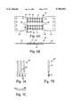
- FIG. 1Ashows, schematically, a conventional reel of carrier parts
- FIG. 1Bis an enlarged detail view of part of the conventional reel of carrier parts shown in FIG. 1A;
- FIG. 2Ais a schematic view of a reel according to the invention containing one form of a carrier support in accordance with the invention
- FIG. 2Bis a plan view of part of the carrier support on the reel of FIG. 2A;
- FIG. 2Cis an enlarged plan view of the carrier support of FIG. 2B;
- FIG. 3is a side view of the carrier support of FIG. 2C;
- FIG. 4is an end view of the carrier support of FIG. 3;
- FIG. 5is a detail view of the carrier support of FIG. 3 along the line 5--5;
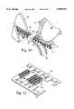
- FIGS. 6A and 6Bare plan and side views of the carrier support after the molding step but before insertion of the pins;
- FIG. 7A, 7B, and 7Care plan, end and side views, respectively, of a strip of pins
- FIG. 8Ais a perspective view schematically illustrating how the strips are molded to the molded bodies of component parts inside a mold section;
- FIG. 8Bis a cross-sectional detail view of part of the mold of FIG. 8A;
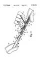
- FIG. 9is a schematic perspective view illustrating the fabrication of a continuous carrier in accordance with the invention.
- FIG. 10is a schematic perspective view illustrating how individual components can be separated from the carrier of FIG. 9 and picked up by a conventional pick-and-place system;
- FIG. 11is a perspective view of part of another series of strip-supported mechanical components, also showing one way of increasing the holding power of the strips;
- FIG. 12is a perspective view of part of another series of strip-supported components, also showing another way of separating a component from the strips;
- FIG. 13shows another form of structure for increasing the holding power of a strip
- FIG. 14is a perspective view of part of another series of carrier-supported components using both a strip and a monofilament
- FIG. 15is an end view of the carrier of FIG. 14.
- FIGS. 1A and 1Bare schematic views of a prior art reeled tape of electrical components.
- the reel 10has reeled up on it a plastic tape 12 which is embossed to form a series of pockets 14 into each of which is placed a separately fabricated electrical component 16.
- the tape 12has a series of sprocket holes 18 along one edge for advancing the tape.
- a plastic cover strip 20is sealed over the filled pockets 14 to prevent the components from falling out when the strip is reeled onto or unreeled from the reel 10.
- the components 16typically have a flat top for receiving the end of a suction head for removing the component from the pocket and placing it on the PCB surface after the cover strip is removed.
- the part 16is at or below the tape surface, making it difficult to use a mechanical gripper to remove the part, as the gripper would have to be inserted into the pocket 14 to grip the component sides below its exposed top.
- the cost of fabricating the embossed tape and assembling the separately made components 16 to the tapeis relatively high.
- a principal feature of the inventionis to encapsulate or attach one or a pair of carrier strips or filaments directly to a side portion of each of the components while a molded pad of the latter is molded.
- the inventioninstead of separately making the electrical components and embossed tape and assembling them, integrates a molding step of the components with attachment of the carrier support to a side portion of each component, hence eliminating the tape embossing step, the assembling step and the attachment of the cover strip step thereby greatly reducing the fabrication cost of a carrier strip loaded with electrical components.
- the inventionallows the use of strips or filaments that are not of the same material as that of the molded component portion, and provides a continuous supply strip of components that allows the components to be readily separated from its supporting strip or filament by simply pulling the component off of its attachment.
- FIG. 2Ashows a reel 21 according to the invention containing one form of a carrier supply strip 22 according to the invention
- FIG. 2Bis an enlarged plan view of part of the carrier strip 22 according to the invention supporting four components 24, in this instance pin headers with two rows of electrically-conductive pins 26.
- spaced plastic strips 28, 30are provided from a reel, having been cut to the desired width and shape indicated in the figure by reference 32.
- the strip widthsdo not have to be the same.
- Along one strip edgeis provided a series of round sprocket holes 34, and along the corresponding edge of the other strip is provided a series of oval sprocket holes 36.
- the round sprocket holes 34are used to advance the strip in controlled steps by any known indexing device such as a controlled sprocket wheel.
- the oval holes 36which are also engaged by a sprocket wheel, are slightly enlarged to accommodate variations and tolerences in the advancing drive.
- the electrical components 24 in this embodimentare pin headers, two of which are shown spaced apart in the longitudinal direction of the carrier, and each of which comprises a molded plastic body 40 perforated with two rows of apertures 41 into which are inserted electrical pins 26.
- Each headerencapsulates edge regions 42 (FIG. 6A) along facing edges of the two strips 28, 30 which thus support the components 24 between the strips.
- the resultant supply strip 22 of edge-supported components 24can now be wound up on the reel 21 for use by a component feeding device used with a mechanical pick-and-place device for gripping the component by one or more of its upstanding pins after it has been separated from its supporting strips 28, 30 for placement on a PCB.
- a stiff plastic cover 44may be detachably assembled to the header 24 to supply the flat top, the cover 44 being removed from the header after the soldering step.
- FIG. 5shows that an alignment notch 46 may be molded into the side of each header 24 to aid the feeder and/or pick-and-place device in locating the header.
- FIGS. 8A, 8B and 9show one way by which the flexible strips 28, 30 can be molded to the header components 24.
- a strip of plastic 48 pre-stamped with the sprocket holes 34, 36is supplied from a reel 50 and advanced by any known indexing mechanism, for example, sprocket wheels and a synchronous drive (not shown), through a conventional stamping die 52 which configures and forms the two side strips 28, 30.
- FIG. 9shows a starting strip 48 with the same width as the final product, and with the stamper 52 removing the center strip section to form the two side strips 28, 30, this is not essential.
- FIGS. 8A and 8BOne way of doing this, which is not to be considered limiting, is illustrated in FIGS. 8A and 8B.
- the strips 28, 30are indexed over the mold base or lower cavity B of an injection mold, the upper cavity A of which is a mirror image of the lower cavity.
- the lower cavitycontains two mold sections 60, each configured to mold one of the header bodies 40.
- Each mold section 60contains along opposite edges recessed regions 61 for receiving a strip (only the recess for the strip 30 is shown).
- the strips 28, 30are clamped between the two mold parts, shown schematically in FIG. 8B.
- each headerWhen molten plastic is injected into the closed mold in the usual way, the plastic body 40 of each header is molded, simultaneously encapsulating the edge regions 42 of both of the flexible strips.
- the apertures 41 in the header body 40may be simultaneously molded by means of core pins (not shown) in the mold halves, or they can be punched in a subsequent step.
- the mold halvesare opened, and the finished assembly 62 ejected from the mold, while simultaneously the assembly 62 is advanced to provide in the opened mold the next strip sections to be encapsulated into the next set of headers to be molded. The process is repeated until molded headers 40 have been attached to and suspended between the strips 28, 30 over their entire length.
- posts 63are provided for alignment of the mold halves.
- pins 63Aare shown in the mold for engagement of the sprocket holes 34 to ensure proper alignment of the strips to the component.
- the pins 63Aare shown enlarged for clarity.
- a recessed area 63Bmay be provided downstream of the cavities 60 for receiving the molded assembly 62 to prevent damage when the mold closes.
- the processing stage 54is in line in the multiple stage processing starting from one supply reel 50 and ending at one take-up reel 21.
- 8Aalso illustrates an alternative scheme wherein, following the processing stage 52, the strips are reeled up to form a further supply reel 50A for processing stage 54, following which the strip-body assembly 62 is reeled up on a take-up reel 50B, which then acts as the supply for the next stage 70, and so on.
- This alternative scheme of reeling and unreeling for one or more stagescan also be applied to the other stages. It will also be understood that, while only two mold cavities 60 have been shown for simplicity, more than two cavities can be employed if desired to increase the number of parts per mold cycle.
- FIGS. 6A and 6BPart of the assembly 62 in this intermediate condition following the molding operation is illustrated in FIGS. 6A and 6B for a dual row header containing seven apertures 41 in each row.
- One of the aperture openingsmay be bevelled 64 for ease of insertion of the pins 26.
- the pins 26can be supplied from a reel 65 as a continuous strip 66 (see FIGS. 7A-7C also) with reduced thickness regions 68 for separation of the pins in a conventional inserter machine 70, illustrated schematically in FIG. 9, which also inserts them into the apertures 40 of the header bodies 40.
- a supply 72 of plastic caps 44 from a reel 74is provided, individual caps 44 separated and attached to the headers 24 in a machine 76, and the modified assembly, which corresponds to the pinned assembly 22 of FIG. 2B, reeled up on a reel 21 typically with interleaf layer 22A for distribution or sale to the PCB fabricator.
- the carrier 22is unreeled from the reel 21 and passed through a device 78 which pushes up (by means not shown) on each of the supporting tabs 29 of each of the strips 28, 30 with enough force, while the strips 28, 30 are tightly held, that the component 24 separates from its carrier strips 28, 30 and, while supported, the component can be picked up by a conventional pick-and-place device 80 having a suction head 82 which contacts and vacuum-attaches to the component cover 44.
- a suction head 82comes into position with each newly-severed component 24 and carries it to the PCB, places the component, and then returns to pick up another component from the carrier 22.
- the carrier strip residues 84, together with the usual paper interleaf 22A,are guided to a separate accumulation area for disposal.
- a feature of the inventionis that electrical or mechanical components of most any size, shape or configuration can be accommodated on the flexible strips, provided that they include along their sides a moldable region, by which is meant a region that is fabricated by molding of a plastic resin and that will attach to the edges 42 of the plastic strips 28, 30.
- the header components 24 having plastic bodies 40they can be made with one, two, or more rows containing anywhere from 2-22 or more pins per row. To realize this merely requires altering the width of each header, represented in FIG. 3 by the dimension 90, and altering the overall width of the assembly, represented in FIG. 3 by the dimension 92.
- the dimension 90can vary between 0.190-2.190 inches
- the dimension 92can vary between 1.260-2.835 inches for typical pin spacings of 0.100 inches. These numbers are merely exemplary and are not to be consided limiting.
- the pull-off forceshould be at least a minimum amount, to ensure that the electrical components 24 do not detach from their carrier during reeling and unfeeling and normal handling before being deliberately separated at a time just before being picked-up by the pick-and-place device 82.
- the pull-off forceshould not exceed a maximum amount, to ensure that any convenient separator force or separating device can be used to reliably separate a component from its carrier strips 28,30 without causing damage to the separated component or the components that remain behind.
- a pull-off force of about 3-5 pounds per sideis adequate to satisfy both requirements.
- This pull-off forceis achieved by a molded region 42 having a length indicated by 94 in FIG. 6A, for components of the size indicated above, preferably of about 0.2 inches, and an overlap indicated by 96 preferably of about 0.015-0.020 inches. Smaller components may use a smaller overlap, and larger components can use a larger overlap.
- the notches 98act to weaken the strip at the region of the notches and thus isolate adjacent components and prevent separating forces applied to one component from being transmitted to and damaging adjacent components.
- the weakened strip regionscan be supplied by a series of perforations.
- FIG. 11shows a plastic part with a screw top 100 mounted beween a pair of carrier strips 102 with opposite side regions of the plastic part 100 molded to the adjacent edges 104 of the carrier strips.
- the flexible strips 28, 30are constituted of a high temperature plastic, such as polyesters commonly known as "Mylar".
- the high temperature propertyis desirable as the strip edges will be subjected to the elevated temperature of the injected molten plastic used for molding the components and encapsulating the strips.
- the molding plasticshould similarly be able to withstand the elevated temperatures of the standard SMT reflow or wave-soldering process that the PCB will be subject to. Molding plastics with this property are well known in the art and are available commercially from suppliers such as GE and DuPont. These and other plastics will be obvious to those skilled in this art.
- the stripsare provided with built in advancing means in the form of the sprocket holes, this is not essential.
- the downstream end of a stripcan be attached to a take-up reel or other pulling device for advancing the strip or filament.
- the edges of the strip or filamentcan be engaged by friction drive means for advancing purposes.
- the inventionis not limited to a pair of strips connected to opposite side regions of each component so that the components are suspended between the strips.
- one side support aloneis sufficient to support a series of such components, for example, a small header with only 1 or 2 positions.
- the componentis separated from the pair of supporting strips by an upward pushing force, which will tear the strip material at the component body, or pull out the strip material from the component body. This is not essential.
- the componentcan be pulled laterally with respect to the longitudinal direction of the carrier to detach it from the carrier.
- the component at the leading edge of the stripcan be pulled off frontwards with a force in the the longitudinal direction of the carrier to detach it from the carrier. While pulling or pushing on the carrier to detach the component from the carrier is preferred, depending upon the component size and the strength of the carrier, the component can also be separated from its carrier supports by pulling or pushing on the component or by severing it from its carrier supports. In any case, no harm results if part of the carrier strip is left in place in the detached component and protrudes from the component side.
- FIG. 12illustrates header assemblies 106 supported by carrier strips 28, 30, with the leading assembly 108 separated from the strips by a force 110 exerted in the longitudinal direction of the strips.
- the attachment between the strip or filament and the moldable edge of the componentis too weak, the attachment can be enhanced by adding holding structure to the strip edge.
- holding structureFor example, as illustrated in FIG. 11, holes 114 can be punched into the strip edge region to be encapsulated. During the molding process, plastic fills the hole and reinforces the strength of the attachment of the component side to the carrier strip.
- FIG. 13shows a modification for the holding structure using small slits 116 in the strip 118 to increase the holding power to the component. This may be desirable when the components are supported by only one side strip 118 or filament.
- Other holding structurecan also be substituted, such as dimples or rough edges or other means to increase the holding surface area.
- a pair of flexible plastic stripsserve as the carrier for the series of components. While preferred, this is not essential.
- the carriercan also be constituted of a single flexible plastic strip attached along one side of each component or of a single or pairs of flexible paper strips or metal strips that will attach to plastic.
- copper or aluminum foil stripsfor example, 0.003-0.005 inches in thickness, are flexible and can be attached by molding to most plastics and can be substituted for the plastic strips.
- the inventionis not limited to strips and can also be implemented by a single flexible filament or pair of filaments, of plastic or metal, which is attached by molding to a side, or encapsulated by molding in the side, of the molded region of a component.
- a weakened region for easy separation of the component from its supporting filamentcan be provided by reduced thickness regions in the filament just above and below where it attaches to each component. This is illustrated in FIGS. 14 and 15, which shows a series of pinless headers 120 each supported at molded side regions 122 by a strip 124 of plastic, metal or fiber on one side, and by a monofilament 126 of plastic or metal molded into the opposite side region 128.
- the resultant supply strip of carrier-supported componentscan be reeled up on a reel for distribution or sale.
- a feature of the inventionis that a large number of components supported as described above can be supplied to the PCB fabricators for handling with the same kind of reel-supplied equipment that is presently in wide use.
- typically such a reel according to the inventionwill comprise at least six feet of a supply strip of components, which depending on component size can amount to hundreds of components supplied via a single reel.
Landscapes
- Engineering & Computer Science (AREA)
- Manufacturing & Machinery (AREA)
- Microelectronics & Electronic Packaging (AREA)
- Injection Moulding Of Plastics Or The Like (AREA)
- Packages (AREA)
- Packaging Frangible Articles (AREA)
- Supply And Installment Of Electrical Components (AREA)
- Manufacturing Of Electrical Connectors (AREA)
Abstract
Description
Claims (18)
Priority Applications (11)
| Application Number | Priority Date | Filing Date | Title |
|---|---|---|---|
| US08/584,534US5706952A (en) | 1996-01-11 | 1996-01-11 | Continuous carrier for electrical or mechanical components |
| TW085115843ATW348146B (en) | 1996-01-11 | 1996-12-21 | Continuous carrier for electrical or mechanical components and method for manufacturing same |
| SG1996011924ASG70582A1 (en) | 1996-01-11 | 1996-12-27 | Continuous carrier for electrical or mechanical components |
| CA002194208ACA2194208C (en) | 1996-01-11 | 1996-12-31 | Continuous carrier for electrical or mechanical components |
| DE69704793TDE69704793T2 (en) | 1996-01-11 | 1997-01-10 | Endless carrier tape for electrical or mechanical components |
| EP97100376AEP0785709B1 (en) | 1996-01-11 | 1997-01-10 | Continuous carrier for electrical or mechanical components |
| KR1019970000567AKR100463665B1 (en) | 1996-01-11 | 1997-01-11 | Continuous Carrier for Electrical or Mechanical Parts |
| JP00357997AJP3815754B2 (en) | 1996-01-11 | 1997-01-13 | Continuous support strip for electrical or mechanical parts |
| US08/794,993US5938996A (en) | 1996-01-11 | 1997-02-05 | Method for making a continuous carrier for electrical or mechanical components |
| US08/843,241US5957739A (en) | 1996-01-11 | 1997-04-14 | Continuous electronic stamping with offset carrier |
| US09/318,534US6202853B1 (en) | 1996-01-11 | 1999-05-25 | Secondary processing for electrical or mechanical components molded to continuous carrier supports |
Applications Claiming Priority (1)
| Application Number | Priority Date | Filing Date | Title |
|---|---|---|---|
| US08/584,534US5706952A (en) | 1996-01-11 | 1996-01-11 | Continuous carrier for electrical or mechanical components |
Related Child Applications (2)
| Application Number | Title | Priority Date | Filing Date |
|---|---|---|---|
| US08/794,993Continuation-In-PartUS5938996A (en) | 1996-01-11 | 1997-02-05 | Method for making a continuous carrier for electrical or mechanical components |
| US08/843,241Continuation-In-PartUS5957739A (en) | 1996-01-11 | 1997-04-14 | Continuous electronic stamping with offset carrier |
Publications (1)
| Publication Number | Publication Date |
|---|---|
| US5706952Atrue US5706952A (en) | 1998-01-13 |
Family
ID=24337713
Family Applications (2)
| Application Number | Title | Priority Date | Filing Date |
|---|---|---|---|
| US08/584,534Expired - LifetimeUS5706952A (en) | 1996-01-11 | 1996-01-11 | Continuous carrier for electrical or mechanical components |
| US08/794,993Expired - LifetimeUS5938996A (en) | 1996-01-11 | 1997-02-05 | Method for making a continuous carrier for electrical or mechanical components |
Family Applications After (1)
| Application Number | Title | Priority Date | Filing Date |
|---|---|---|---|
| US08/794,993Expired - LifetimeUS5938996A (en) | 1996-01-11 | 1997-02-05 | Method for making a continuous carrier for electrical or mechanical components |
Country Status (8)
| Country | Link |
|---|---|
| US (2) | US5706952A (en) |
| EP (1) | EP0785709B1 (en) |
| JP (1) | JP3815754B2 (en) |
| KR (1) | KR100463665B1 (en) |
| CA (1) | CA2194208C (en) |
| DE (1) | DE69704793T2 (en) |
| SG (1) | SG70582A1 (en) |
| TW (1) | TW348146B (en) |
Cited By (16)
| Publication number | Priority date | Publication date | Assignee | Title |
|---|---|---|---|---|
| US5884773A (en)* | 1997-03-21 | 1999-03-23 | Unimet Gmbh | Carrier strip and method of its manufacturing |
| US5956925A (en)* | 1997-12-31 | 1999-09-28 | Bmi, Inc. | Carrier tape and method for washing of components in carrier tape |
| US5967365A (en)* | 1997-08-01 | 1999-10-19 | Autosplice Systems, Inc. | Feeder for separating parts molded to a continuous carrier tape |
| US6224399B1 (en)* | 1999-05-14 | 2001-05-01 | Weco Electrical Connectors Inc. | Surface-mount electrical connection device |
| US20020047385A1 (en)* | 1998-11-20 | 2002-04-25 | Matsushita Electric Industrial Co., Ltd. | Brushless motor and its assembly method |
| US6601729B1 (en) | 1999-03-26 | 2003-08-05 | Papp Enterprises, Llc | Automated portable medication radial dispensing apparatus and method using a carrier tape |
| US20040093721A1 (en)* | 2002-11-20 | 2004-05-20 | Jeffrey Watson | Electronic package carrier tape |
| US20090040515A1 (en)* | 2003-10-30 | 2009-02-12 | Bayer Healthcare Llc | Formats For Optical Analysis And Methods Of Manufacturing The Same |
| US20090067149A1 (en)* | 2007-09-07 | 2009-03-12 | Robert Bogursky | Electronic shielding apparatus and methods |
| US20100157566A1 (en)* | 2008-12-19 | 2010-06-24 | Robert Bogursky | Electronic shield assembly and methods |
| US20110223377A1 (en)* | 2009-01-09 | 2011-09-15 | Ann Lambrechts | Longitudinal belt with reinforcing fibres |
| US8226904B2 (en) | 2003-10-30 | 2012-07-24 | Bayer Healthcare Llc | Optical format with platform-and-well construction |
| US9120257B2 (en) | 2013-01-11 | 2015-09-01 | Apple Inc. | Composite carrier frame for plastic injection molding |
| WO2019089879A1 (en)* | 2017-11-02 | 2019-05-09 | Universal Instruments Corporation | Fixture to hold part before and after reflow, and method |
| CN110978354A (en)* | 2019-12-31 | 2020-04-10 | 青岛慕沃科技有限公司 | Tire belt layer forming mold and forming process using same |
| CN113710590A (en)* | 2019-04-26 | 2021-11-26 | 住友电装株式会社 | Connector housing keeping structure and connector cover keeping structure |
Families Citing this family (16)
| Publication number | Priority date | Publication date | Assignee | Title |
|---|---|---|---|---|
| US6547452B1 (en) | 2000-05-11 | 2003-04-15 | International Business Machines Corporation | Alignment systems for subassemblies of overmolded optoelectronic modules |
| US6365434B1 (en)* | 2000-06-28 | 2002-04-02 | Micron Technology, Inc. | Method and apparatus for reduced flash encapsulation of microelectronic devices |
| KR20040032316A (en)* | 2002-10-09 | 2004-04-17 | 쵸우수안 차이 | Shifting Device for Manufacturing Continuous Terminals |
| US20050025848A1 (en)* | 2003-07-30 | 2005-02-03 | Ruey-Fa Huang | Air filter shaping mold |
| US20060172610A1 (en)* | 2005-02-01 | 2006-08-03 | Keisuke Sakai | Method and apparatus for terminal row insert molding |
| US7650914B2 (en) | 2006-06-22 | 2010-01-26 | Autosplice, Inc. | Apparatus and methods for filament crimping and manufacturing |
| US8117725B2 (en)* | 2008-10-31 | 2012-02-21 | The Gillette Company | Method of manufacturing a plurality of molded components |
| US8851443B2 (en) | 2010-12-15 | 2014-10-07 | Autosplice, Inc. | Memory alloy-actuated apparatus and methods for making and using the same |
| EP2771969A4 (en) | 2011-10-26 | 2015-09-16 | Autosplice Inc | Shape memory alloy powered apparatus and method for making and constructing the apparatus |
| DE102016225973B4 (en)* | 2016-12-22 | 2019-06-13 | Conti Temic Microelectronic Gmbh | Method for contacting a contact surface on a flexible printed circuit board with a metal contact, connection of flexible printed circuit board and metal contact and control unit |
| CN109606900B (en)* | 2016-12-30 | 2020-06-05 | 乐清市华尊电气有限公司 | Portable PCB board rack |
| US11739737B2 (en) | 2018-02-07 | 2023-08-29 | Autosplice, Inc. | Shape memory alloy filament crimping element |
| DE102019131150A1 (en)* | 2019-11-19 | 2021-05-20 | Te Connectivity Germany Gmbh | Component packing of technical components as well as technical components |
| DE102020205112A1 (en) | 2020-04-22 | 2021-10-28 | Te Connectivity Germany Gmbh | Strips of blind plugs in a row for a plug |
| WO2021263121A1 (en)* | 2020-06-25 | 2021-12-30 | Jabil Inc. | Apparatus, system and method for cutting and delivering stamped contacts |
| KR102727419B1 (en)* | 2022-01-07 | 2024-11-07 | 이준호 | Apparatus and Method for Feeding Surface Mounted Devices, and Surface Mounted Device Strip Thereof |
Citations (8)
| Publication number | Priority date | Publication date | Assignee | Title |
|---|---|---|---|---|
| US3606000A (en)* | 1968-07-03 | 1971-09-20 | Amp Inc | Thermoformed plastic covered connectors |
| US3625352A (en)* | 1969-10-22 | 1971-12-07 | Spotnails | Laminated fastener strip having inner and outer laminae of disparate melting points |
| US3711931A (en)* | 1971-04-01 | 1973-01-23 | Multifastener Corp | Method of forming fastener strip |
| US4417396A (en)* | 1981-11-02 | 1983-11-29 | Elfab Corporation | Method for manufacturing integrated circuit connectors |
| US4422708A (en)* | 1980-06-13 | 1983-12-27 | Ultra-Precision, S.A. | Support device for integrated circuit |
| US4480150A (en)* | 1982-07-12 | 1984-10-30 | Motorola Inc. | Lead frame and method |
| US4901854A (en)* | 1988-09-29 | 1990-02-20 | Dennison Manufacturing Company | Loop connected attachments |
| US5303821A (en)* | 1992-11-06 | 1994-04-19 | Ayres Donald B | Resilient clip assembly |
Family Cites Families (14)
| Publication number | Priority date | Publication date | Assignee | Title |
|---|---|---|---|---|
| US3672046A (en)* | 1970-01-14 | 1972-06-27 | Technitrol Inc | The method of making an electrical component |
| US3913195A (en)* | 1974-05-28 | 1975-10-21 | William D Beaver | Method of making piezoelectric devices |
| US4012835A (en)* | 1974-09-17 | 1977-03-22 | E. I. Du Pont De Nemours And Co. | Method of forming a dual in-line package |
| US4812421A (en)* | 1987-10-26 | 1989-03-14 | Motorola, Inc. | Tab-type semiconductor process |
| US4793060A (en)* | 1984-12-13 | 1988-12-27 | Minnesota Mining And Manufacturing Company | Manufacture of low profile clip connector |
| FR2593320B1 (en)* | 1986-01-21 | 1988-03-04 | Europ Composants Electron | METHOD FOR MANUFACTURING AN INDUCTIVE COMPONENT FOR FLAT CARRYING |
| FR2598258B1 (en)* | 1986-04-30 | 1988-10-07 | Aix Les Bains Composants | METHOD OF ENCAPSULATING INTEGRATED CIRCUITS. |
| US4832622A (en) | 1987-01-23 | 1989-05-23 | Autosplice, Inc. | Endless electrical connector |
| US4816426A (en)* | 1987-02-19 | 1989-03-28 | Olin Corporation | Process for manufacturing plastic pin grid arrays and the product produced thereby |
| JPH01137091U (en)* | 1988-03-12 | 1989-09-19 | ||
| JPH04273112A (en)* | 1991-02-28 | 1992-09-29 | Murata Mfg Co Ltd | Molded chip electronic component |
| US5286426A (en)* | 1992-04-01 | 1994-02-15 | Allegro Microsystems, Inc. | Assembling a lead frame between a pair of molding cavity plates |
| US5263241A (en)* | 1992-04-06 | 1993-11-23 | Delco Electronics Corporation | Apparatus useful in the manufacture of a pressure sensor assembly |
| US8457993B1 (en) | 2010-03-11 | 2013-06-04 | Safe Deposit Box Insurance Coverage, LLC | Insurance for a safe deposit box |
- 1996
- 1996-01-11USUS08/584,534patent/US5706952A/ennot_activeExpired - Lifetime
- 1996-12-21TWTW085115843Apatent/TW348146B/ennot_activeIP Right Cessation
- 1996-12-27SGSG1996011924Apatent/SG70582A1/enunknown
- 1996-12-31CACA002194208Apatent/CA2194208C/ennot_activeExpired - Fee Related
- 1997
- 1997-01-10EPEP97100376Apatent/EP0785709B1/ennot_activeExpired - Lifetime
- 1997-01-10DEDE69704793Tpatent/DE69704793T2/ennot_activeExpired - Fee Related
- 1997-01-11KRKR1019970000567Apatent/KR100463665B1/ennot_activeExpired - Fee Related
- 1997-01-13JPJP00357997Apatent/JP3815754B2/ennot_activeExpired - Fee Related
- 1997-02-05USUS08/794,993patent/US5938996A/ennot_activeExpired - Lifetime
Patent Citations (8)
| Publication number | Priority date | Publication date | Assignee | Title |
|---|---|---|---|---|
| US3606000A (en)* | 1968-07-03 | 1971-09-20 | Amp Inc | Thermoformed plastic covered connectors |
| US3625352A (en)* | 1969-10-22 | 1971-12-07 | Spotnails | Laminated fastener strip having inner and outer laminae of disparate melting points |
| US3711931A (en)* | 1971-04-01 | 1973-01-23 | Multifastener Corp | Method of forming fastener strip |
| US4422708A (en)* | 1980-06-13 | 1983-12-27 | Ultra-Precision, S.A. | Support device for integrated circuit |
| US4417396A (en)* | 1981-11-02 | 1983-11-29 | Elfab Corporation | Method for manufacturing integrated circuit connectors |
| US4480150A (en)* | 1982-07-12 | 1984-10-30 | Motorola Inc. | Lead frame and method |
| US4901854A (en)* | 1988-09-29 | 1990-02-20 | Dennison Manufacturing Company | Loop connected attachments |
| US5303821A (en)* | 1992-11-06 | 1994-04-19 | Ayres Donald B | Resilient clip assembly |
Cited By (26)
| Publication number | Priority date | Publication date | Assignee | Title |
|---|---|---|---|---|
| US5884773A (en)* | 1997-03-21 | 1999-03-23 | Unimet Gmbh | Carrier strip and method of its manufacturing |
| US5967365A (en)* | 1997-08-01 | 1999-10-19 | Autosplice Systems, Inc. | Feeder for separating parts molded to a continuous carrier tape |
| US5956925A (en)* | 1997-12-31 | 1999-09-28 | Bmi, Inc. | Carrier tape and method for washing of components in carrier tape |
| US20020047385A1 (en)* | 1998-11-20 | 2002-04-25 | Matsushita Electric Industrial Co., Ltd. | Brushless motor and its assembly method |
| US6624540B2 (en)* | 1998-11-20 | 2003-09-23 | Matsushita Electric Industrial Co., Ltd. | Packaging for automated supply of a brushless motor |
| US6601729B1 (en) | 1999-03-26 | 2003-08-05 | Papp Enterprises, Llc | Automated portable medication radial dispensing apparatus and method using a carrier tape |
| US6224399B1 (en)* | 1999-05-14 | 2001-05-01 | Weco Electrical Connectors Inc. | Surface-mount electrical connection device |
| US20040093721A1 (en)* | 2002-11-20 | 2004-05-20 | Jeffrey Watson | Electronic package carrier tape |
| US20050016898A1 (en)* | 2002-11-20 | 2005-01-27 | Jeffrey Watson | Electronic package carrier tape |
| US7127805B2 (en) | 2002-11-20 | 2006-10-31 | Intel Corporation | Electronic device carrier and manufacturing tape |
| US7228622B2 (en) | 2002-11-20 | 2007-06-12 | Intel Corporation | Electronic device carrier and manufacture tape |
| US7494620B2 (en) | 2003-10-30 | 2009-02-24 | Bayer Healthcare Llc | Formats for optical analysis and methods of manufacturing the same |
| US7731897B2 (en) | 2003-10-30 | 2010-06-08 | Bayer Healthcare Llc | Formats for optical analysis and methods of manufacturing the same |
| US20090040515A1 (en)* | 2003-10-30 | 2009-02-12 | Bayer Healthcare Llc | Formats For Optical Analysis And Methods Of Manufacturing The Same |
| US8226904B2 (en) | 2003-10-30 | 2012-07-24 | Bayer Healthcare Llc | Optical format with platform-and-well construction |
| US8031485B2 (en) | 2007-09-07 | 2011-10-04 | Autosplice, Inc. | Electronic shielding apparatus and methods |
| US20090067149A1 (en)* | 2007-09-07 | 2009-03-12 | Robert Bogursky | Electronic shielding apparatus and methods |
| US20100157566A1 (en)* | 2008-12-19 | 2010-06-24 | Robert Bogursky | Electronic shield assembly and methods |
| US20110223377A1 (en)* | 2009-01-09 | 2011-09-15 | Ann Lambrechts | Longitudinal belt with reinforcing fibres |
| US8877346B2 (en)* | 2009-01-09 | 2014-11-04 | Nv Bekaert Sa | Longitudinal belt with reinforcing fibres |
| US9120257B2 (en) | 2013-01-11 | 2015-09-01 | Apple Inc. | Composite carrier frame for plastic injection molding |
| WO2019089879A1 (en)* | 2017-11-02 | 2019-05-09 | Universal Instruments Corporation | Fixture to hold part before and after reflow, and method |
| US11363725B2 (en) | 2017-11-02 | 2022-06-14 | Universal Instruments Corporation | Fixture to hold part before and after reflow, and method |
| CN113710590A (en)* | 2019-04-26 | 2021-11-26 | 住友电装株式会社 | Connector housing keeping structure and connector cover keeping structure |
| CN110978354A (en)* | 2019-12-31 | 2020-04-10 | 青岛慕沃科技有限公司 | Tire belt layer forming mold and forming process using same |
| CN110978354B (en)* | 2019-12-31 | 2024-04-09 | 南通奥福路科技有限公司 | Tire belt layer forming die and forming process using same |
Also Published As
| Publication number | Publication date |
|---|---|
| EP0785709B1 (en) | 2001-05-16 |
| CA2194208C (en) | 2005-10-18 |
| TW348146B (en) | 1998-12-21 |
| JPH09312495A (en) | 1997-12-02 |
| DE69704793T2 (en) | 2001-10-11 |
| KR970060585A (en) | 1997-08-12 |
| SG70582A1 (en) | 2000-02-22 |
| EP0785709A3 (en) | 1998-05-20 |
| EP0785709A2 (en) | 1997-07-23 |
| US5938996A (en) | 1999-08-17 |
| DE69704793D1 (en) | 2001-06-21 |
| JP3815754B2 (en) | 2006-08-30 |
| CA2194208A1 (en) | 1997-07-12 |
| KR100463665B1 (en) | 2006-06-22 |
Similar Documents
| Publication | Publication Date | Title |
|---|---|---|
| US5706952A (en) | Continuous carrier for electrical or mechanical components | |
| CA1168764A (en) | Encapsulation for semiconductor integrated circuit chip | |
| KR100550407B1 (en) | One Touch Connectors and One Touch Connector Assemblies | |
| US5822855A (en) | Method of making electrical connector having a two part articulated housing | |
| US4099615A (en) | Carrier strip mounted electrical components | |
| CA2304537A1 (en) | Microelectronic component carrier and method of its manufacture | |
| US4214353A (en) | Method of assembling heated terminals and rolled film capacitors within plastic boxes | |
| US5199564A (en) | Carrier tape for electronic through-hole components | |
| CA1112312A (en) | Carrier strip for round lead pins and method for making same | |
| EP0235925A2 (en) | Surface-mountable package for encapsulated tap-automated-bonded integrated circuit modules | |
| EP0756448B1 (en) | Electronic component carrier tape with generic pockets | |
| US6202853B1 (en) | Secondary processing for electrical or mechanical components molded to continuous carrier supports | |
| EP0128016A2 (en) | Carrier assembly and method of making same | |
| US5351821A (en) | Carrier tape with generic pockets | |
| US6436517B1 (en) | Continuous molded electronic circuits | |
| EP0457984B1 (en) | Pin-holding device for use in connecting a pin | |
| JPH11251347A (en) | Manufacture of semiconductor package | |
| JPS63308863A (en) | Method of packaging batteries | |
| CA1063218A (en) | Mounting of dual-in-line electronic packages | |
| JPH05310264A (en) | Tape for packing electronic parts | |
| US20040229507A1 (en) | Miniature contact block packaging for printed circuit | |
| JP2637369B2 (en) | Electronic component taping method | |
| CN1047421A (en) | Modular connector system with contact element of high density surface installation | |
| JPH0432774Y2 (en) | ||
| JPS6381913A (en) | Manufacture of miniature coil |
Legal Events
| Date | Code | Title | Description |
|---|---|---|---|
| AS | Assignment | Owner name:AUTOSPLICE SYSTEMS INC., CALIFORNIA Free format text:ASSIGNMENT OF ASSIGNORS INTEREST;ASSIGNORS:BIANCA, GIUSEPPE;BOGURSKY, ROBERT M.;REEL/FRAME:007836/0060 Effective date:19960104 | |
| STCF | Information on status: patent grant | Free format text:PATENTED CASE | |
| FPAY | Fee payment | Year of fee payment:4 | |
| FPAY | Fee payment | Year of fee payment:8 | |
| FEPP | Fee payment procedure | Free format text:PAT HOLDER NO LONGER CLAIMS SMALL ENTITY STATUS, ENTITY STATUS SET TO UNDISCOUNTED (ORIGINAL EVENT CODE: STOL); ENTITY STATUS OF PATENT OWNER: LARGE ENTITY | |
| REMI | Maintenance fee reminder mailed | ||
| FPAY | Fee payment | Year of fee payment:12 | |
| SULP | Surcharge for late payment | Year of fee payment:11 | |
| SULP | Surcharge for late payment | ||
| AS | Assignment | Owner name:MEDLEY CAPITAL CORPORATION, AS AGENT, NEW YORK Free format text:SECURITY INTEREST;ASSIGNOR:AUTOSPLICE, INC.;REEL/FRAME:033263/0447 Effective date:20140630 | |
| AS | Assignment | Owner name:WELLS FARGO BANK NATIONAL ASSOCIATION, CALIFORNIA Free format text:SECURITY INTEREST;ASSIGNOR:AUTOSPLICE, INC.;REEL/FRAME:034587/0542 Effective date:20140917 | |
| AS | Assignment | Owner name:AUTOSPLICE, INC., CALIFORNIA Free format text:RELEASE AND TERMINATION OF SECURITY INTERESTS IN PATENTS;ASSIGNOR:MEDLEY CAPITAL CORPORATION, AS AGENT;REEL/FRAME:058957/0300 Effective date:20211122 |