US5703363A - Infrared to visible light image conversion device - Google Patents
Infrared to visible light image conversion deviceDownload PDFInfo
- Publication number
- US5703363A US5703363AUS08/638,006US63800696AUS5703363AUS 5703363 AUS5703363 AUS 5703363AUS 63800696 AUS63800696 AUS 63800696AUS 5703363 AUS5703363 AUS 5703363A
- Authority
- US
- United States
- Prior art keywords
- array
- image
- light emitting
- quantum well
- emitting diodes
- Prior art date
- Legal status (The legal status is an assumption and is not a legal conclusion. Google has not performed a legal analysis and makes no representation as to the accuracy of the status listed.)
- Expired - Lifetime
Links
Images

Classifications
- H—ELECTRICITY
- H01—ELECTRIC ELEMENTS
- H01J—ELECTRIC DISCHARGE TUBES OR DISCHARGE LAMPS
- H01J29/00—Details of cathode-ray tubes or of electron-beam tubes of the types covered by group H01J31/00
- H01J29/02—Electrodes; Screens; Mounting, supporting, spacing or insulating thereof
- H01J29/10—Screens on or from which an image or pattern is formed, picked up, converted or stored
- H01J29/36—Photoelectric screens; Charge-storage screens
- H01J29/38—Photoelectric screens; Charge-storage screens not using charge storage, e.g. photo-emissive screen, extended cathode
- H01J29/385—Photocathodes comprising a layer which modified the wave length of impinging radiation
- B—PERFORMING OPERATIONS; TRANSPORTING
- B82—NANOTECHNOLOGY
- B82Y—SPECIFIC USES OR APPLICATIONS OF NANOSTRUCTURES; MEASUREMENT OR ANALYSIS OF NANOSTRUCTURES; MANUFACTURE OR TREATMENT OF NANOSTRUCTURES
- B82Y20/00—Nanooptics, e.g. quantum optics or photonic crystals
- H—ELECTRICITY
- H01—ELECTRIC ELEMENTS
- H01J—ELECTRIC DISCHARGE TUBES OR DISCHARGE LAMPS
- H01J31/00—Cathode ray tubes; Electron beam tubes
- H01J31/08—Cathode ray tubes; Electron beam tubes having a screen on or from which an image or pattern is formed, picked up, converted, or stored
- H01J31/50—Image-conversion or image-amplification tubes, i.e. having optical, X-ray, or analogous input, and optical output
- H01J31/505—Image-conversion or image-amplification tubes, i.e. having optical, X-ray, or analogous input, and optical output flat tubes, e.g. proximity focusing tubes
- H—ELECTRICITY
- H01—ELECTRIC ELEMENTS
- H01L—SEMICONDUCTOR DEVICES NOT COVERED BY CLASS H10
- H01L25/00—Assemblies consisting of a plurality of semiconductor or other solid state devices
- H01L25/16—Assemblies consisting of a plurality of semiconductor or other solid state devices the devices being of types provided for in two or more different subclasses of H10B, H10D, H10F, H10H, H10K or H10N, e.g. forming hybrid circuits
- H01L25/167—Assemblies consisting of a plurality of semiconductor or other solid state devices the devices being of types provided for in two or more different subclasses of H10B, H10D, H10F, H10H, H10K or H10N, e.g. forming hybrid circuits comprising optoelectronic devices, e.g. LED, photodiodes
- H—ELECTRICITY
- H10—SEMICONDUCTOR DEVICES; ELECTRIC SOLID-STATE DEVICES NOT OTHERWISE PROVIDED FOR
- H10F—INORGANIC SEMICONDUCTOR DEVICES SENSITIVE TO INFRARED RADIATION, LIGHT, ELECTROMAGNETIC RADIATION OF SHORTER WAVELENGTH OR CORPUSCULAR RADIATION
- H10F77/00—Constructional details of devices covered by this subclass
- H10F77/10—Semiconductor bodies
- H10F77/14—Shape of semiconductor bodies; Shapes, relative sizes or dispositions of semiconductor regions within semiconductor bodies
- H10F77/146—Superlattices; Multiple quantum well structures
- H—ELECTRICITY
- H01—ELECTRIC ELEMENTS
- H01J—ELECTRIC DISCHARGE TUBES OR DISCHARGE LAMPS
- H01J2231/00—Cathode ray tubes or electron beam tubes
- H01J2231/50—Imaging and conversion tubes
- H01J2231/50005—Imaging and conversion tubes characterised by form of illumination
- H01J2231/5001—Photons
- H01J2231/50015—Light
- H01J2231/50026—Infrared
- H—ELECTRICITY
- H01—ELECTRIC ELEMENTS
- H01J—ELECTRIC DISCHARGE TUBES OR DISCHARGE LAMPS
- H01J2231/00—Cathode ray tubes or electron beam tubes
- H01J2231/50—Imaging and conversion tubes
- H01J2231/50057—Imaging and conversion tubes characterised by form of output stage
- H01J2231/50063—Optical
- H—ELECTRICITY
- H01—ELECTRIC ELEMENTS
- H01L—SEMICONDUCTOR DEVICES NOT COVERED BY CLASS H10
- H01L2924/00—Indexing scheme for arrangements or methods for connecting or disconnecting semiconductor or solid-state bodies as covered by H01L24/00
- H01L2924/0001—Technical content checked by a classifier
- H01L2924/0002—Not covered by any one of groups H01L24/00, H01L24/00 and H01L2224/00
Definitions
- the present inventionrelates to image conversion systems. More specifically, the present invention relates to infrared to visible light image conversion systems.
- Infrared to visible light image conversion systemsare used in thermal sights for armored vehicles and small weapons and in night driving devices.
- Present infrared to visible light image conversion systemsoperate by convening an infrared signal to a scanned image which is then convened into a visible image.
- Current image conversion systemsuse either scanned or staring columns of infrared detectors or staring arrays of infrared detectors followed by electronic processing. The detected image is then electronically read out, processed, and convened back into an optical image.
- the optical imageis typically formed by either a scanned light emitting diode array or a cathode ray tube.
- the need in the artis addressed by the image conversion device of the present invention, which provides a smaller, less complex infrared to visible light conversion requiring no external processing.
- the inventive deviceincludes an infrared detector and an infrared to visible image converter on the same substrate.
- the detectorincludes an array of multiple quantum well detectors based on gallium arsenide (GaAs) and related materials and the image converter includes an array of light emitting diodes also formed of GaAs and related materials deposited on the array of multiple quantum well detectors.
- GaAsgallium arsenide
- a photoemissive surfacemay be formed on the array of light emitting diodes and a phosphor screen used to display the visible image or the light emitting diode array can directly display a visible image.
- FIG. 1is a cross-sectional view of a first embodiment of an image conversion system of the present invention.
- FIG. 2is a cross-sectional view of a second embodiment of the image conversion system of the present invention.
- FIG. 3is a cross-sectional view of an image conversion device of the present invention.
- FIG. 4is a cross-sectional view of a third embodiment of the image conversion system of the present invention.
- FIG. 5is a cross-sectional view of an unbiased band structure of the image conversion device of the present invention.
- FIG. 6is a cross-sectional view of a biased band structure of the image conversion device of the present invention.
- the image conversion device of the present inventionis suitable for use in thermal sights for armored vehicles, thermal sights for small arms, and night driving devices.
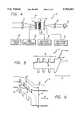
- FIG. 1shows a first embodiment of an image conversion system 10 of the present invention.
- An objective 12is an imaging lens, or may be a mirror and lens combination.
- a suitable objective 12would have a focal length of one to two inches, with an f-number of one.
- a detector/emitter array 14is fabricated as a monolithic assembly with the emitters 14 fabricated by substrate deposition of successive layers of semiconductor materials such as GaAs and gallium aluminum arsenide (GaAlAs) to detect infrared energy, and other semiconductor materials such as GaAs, GaAsP or GaP to emit visible light.
- semiconductor materialssuch as GaAs and gallium aluminum arsenide (GaAlAs) to detect infrared energy, and other semiconductor materials such as GaAs, GaAsP or GaP to emit visible light.
- An ocular 16is a lens which may be similar to the objective 12 if a one-to-one magnification is desired, or have a shorter focal length than the objective 12 if magnification is required.
- a suitable ocular 16such as a telescope eyepiece, would have a focal length of one to two inches, with an f-number of two or three, for comfortable viewing by a human eye 18.
- a cryogenic cooler 20 of standard designmaintains the detector/emitter array 14 at its proper operating temperature.
- the bias supplies 22 which provide bias to the detector/emitter array 14are low voltage, under 10 volts.
- the embodiment of the image conversion system 10 depicted in FIG. 1has overall quantum efficiency considerably less than one.
- FIG. 2depicts a second embodiment of the image conversion system 10 which includes an image conversion device 100 of the present invention.
- the objective 12, the ocular 16, the cryogenic cooler 20, and the array bias supplies 22are as described above.
- the emitters 14are fabricated of GaAs, which emits in the near infrared region.
- the detector/emitter array 14is also coated with a photoemissive surface 28 such as silver cesium oxide (S1), formed by the vacuum deposition of cesium and silver which are oxidized in a vacuum under heat or by sputtering. Other photoemissive surfaces can also be used.
- a vacuum envelope 26surrounds the detector/emitter array 14, the photoemissive surface 28 and a phosphor screen 30.
- a high voltage power supply 24is a high voltage source, in the 1000 to 2000 volt range, for accelerating photoelectrons emitted by the photoemissive surface 28 adjacent to the detector/emitter array 14.
- the phosphor screen 30is positioned to receive accelerated photoelectrons and is capable of emitting visible light which can be detected by the eye 18. This embodiment provides an improvement in quantum efficiency over the first embodiment of the image conversion system 10 depicted in FIG. 1, since the GaAs emitter 14 is more efficient and the phosphor screen 30 is capable of emitting several photons for each incident electron.
- FIG. 3depicts in greater detail the image conversion device 100 of the present invention.
- An array of detectors/emitters 14is formed on a GaAs substrate 36 by depositing successive layers of GaAs and GaAlAs or other suitable materials.
- the lower layersform multiple quantum well detectors 38 tuned to the 9 to 11 micron or 3 to 5 micron region.
- the upper layersform GaAs or GaAsP light emitting diodes 40 capable of emitting in the 0.6 to 1 micron range, within the near infrared or visible spectral region.
- the photoemissive surface 28 sensitive to this spectral rangeis deposited over the light emitting diodes 40.
- a silver substrate 46is formed next, with the photoemissive surface 28 deposited thereon.
- the accelerating voltage 24is provided to accelerate electrons from the photoemissive surface 28 onto the phosphor screen 30, which is formed on a glass substrate 44.
- the detectors/emitters 14 and phosphor screen 30are enclosed in vacuum envelope 26 and cooled to cryogenic temperatures by cryogenic cooler 20.
- FIG. 4depicts a third embodiment of the image conversion system 10 of the present invention.
- the objective 12, the detector/emitter array 14, the ocular 16, the cryogenic cooler 20, the array bias supplies 22, the high voltage power supply 24, the vacuum envelop 26, the photoemissive surface 28, and the phosphor screen 30are as described above.
- Sensitivityis further increased by inclusion of an electron multiplier 32 of the microchannel type between the photoemissive surface 28 and the phosphor screen 30.
- the electron multiplier 32is powered by a multiplier power supply 34 which is a high voltage source, in the 1000 to 2000 volt range.
- Photons in the 9 to 11 micron rangeare focused through the GaAs substrate 36 onto the array of multiple quantum well detectors 38.
- the excited electrons in each detectorare transferred to light emitting diodes 40.
- the photons emitted by the light emitting diodes 40are absorbed by the photoemissive surface 28 which emits photoelectrons into vacuum envelope 26.
- the photoelectronsare accelerated by accelerating voltage 24 into the phosphor screen 30 to provide a visible image.
- FIG. 5shows the composition and band structure of the detector/emitters 14 with no bias applied.
- FIG. 6shows the composition and band structure of the detector/emitters 14 with bias applied.
- a 10 micron photonenters through the GaAs substrate 36 and is absorbed by an electron in one of the quantum wells 38 (1). The photon excites the electron to a level above the well 38 barriers (transition from 1 to 2). The electron is then moved by the bias potential to the light emitting diode region 40 (transition from 2 to 3). The electron then crosses the band gap 48 to occupy an empty state below the band gap 48 (transition from 3 to 4), and in the process emits a photon in the 0.6 to 1 micron range, depending on the band gap.
- This photonis used to stimulate a photoelectron as shown in FIG. 3. If sufficient 10 micron photons are present, the light emitting diode 40 can be arranged to emit in the visible region, and this image can be used directly without the photoemissive surface or phosphor screen.
- the need in the artis thus addressed by the image conversion device of the present invention, which provides a smaller, less complex infrared to visible light conversion requiring no external processing.
Landscapes
- Engineering & Computer Science (AREA)
- Nanotechnology (AREA)
- Chemical & Material Sciences (AREA)
- Physics & Mathematics (AREA)
- Microelectronics & Electronic Packaging (AREA)
- Crystallography & Structural Chemistry (AREA)
- Power Engineering (AREA)
- Condensed Matter Physics & Semiconductors (AREA)
- Optics & Photonics (AREA)
- Life Sciences & Earth Sciences (AREA)
- Computer Hardware Design (AREA)
- Biophysics (AREA)
- General Physics & Mathematics (AREA)
- Photometry And Measurement Of Optical Pulse Characteristics (AREA)
- Transforming Light Signals Into Electric Signals (AREA)
- Radiation Pyrometers (AREA)
Abstract
Description
Claims (16)
Priority Applications (5)
| Application Number | Priority Date | Filing Date | Title |
|---|---|---|---|
| US08/638,006US5703363A (en) | 1996-04-25 | 1996-04-25 | Infrared to visible light image conversion device |
| IL12069597AIL120695A (en) | 1996-04-25 | 1997-04-17 | Infrared to visible light image conversion device |
| DE69719234TDE69719234T2 (en) | 1996-04-25 | 1997-04-25 | Image conversion device for infrared into visible light |
| JP9108900AJP3021388B2 (en) | 1996-04-25 | 1997-04-25 | A device that converts infrared images into visible light images |
| EP97302843AEP0803910B1 (en) | 1996-04-25 | 1997-04-25 | Infrared to visible light image conversion device |
Applications Claiming Priority (1)
| Application Number | Priority Date | Filing Date | Title |
|---|---|---|---|
| US08/638,006US5703363A (en) | 1996-04-25 | 1996-04-25 | Infrared to visible light image conversion device |
Publications (1)
| Publication Number | Publication Date |
|---|---|
| US5703363Atrue US5703363A (en) | 1997-12-30 |
Family
ID=24558262
Family Applications (1)
| Application Number | Title | Priority Date | Filing Date |
|---|---|---|---|
| US08/638,006Expired - LifetimeUS5703363A (en) | 1996-04-25 | 1996-04-25 | Infrared to visible light image conversion device |
Country Status (5)
| Country | Link |
|---|---|
| US (1) | US5703363A (en) |
| EP (1) | EP0803910B1 (en) |
| JP (1) | JP3021388B2 (en) |
| DE (1) | DE69719234T2 (en) |
| IL (1) | IL120695A (en) |
Cited By (6)
| Publication number | Priority date | Publication date | Assignee | Title |
|---|---|---|---|---|
| US5808799A (en)* | 1996-10-31 | 1998-09-15 | Raytheon Ti Systems, Inc. | Infrared lens assembly with athermalization element and method |
| WO2000075714A1 (en)* | 1999-06-04 | 2000-12-14 | Litton Systems, Inc. | Black-out curtain |
| US20040151847A1 (en)* | 2002-12-26 | 2004-08-05 | Nec Tokin Corporation | Ornamental material performing particular light emission or particular color emission |
| WO2008038181A3 (en)* | 2006-09-28 | 2008-06-12 | Philips Intellectual Property | Solid-state light source with color feedback and combined communication means |
| DE102005054146B4 (en)* | 2005-11-14 | 2009-03-26 | Marchanka, Valery M., Dr.-Ing. | Image converter for converting the spectrum of an optical image |
| US20240302709A1 (en)* | 2021-02-01 | 2024-09-12 | Northwestern University | Wavelength converting natural vision system |
Families Citing this family (1)
| Publication number | Priority date | Publication date | Assignee | Title |
|---|---|---|---|---|
| DE102017223115A1 (en) | 2017-12-18 | 2019-06-19 | Carl Zeiss Microscopy Gmbh | Secondary electron multiplier and its use |
Citations (4)
| Publication number | Priority date | Publication date | Assignee | Title |
|---|---|---|---|---|
| US2929934A (en)* | 1954-12-30 | 1960-03-22 | Rca Corp | Radiant energy sensitive device |
| US4205227A (en)* | 1976-11-26 | 1980-05-27 | Texas Instruments Incorporated | Single junction emitter array |
| US5036197A (en)* | 1988-12-13 | 1991-07-30 | Thorn Emi Electronics Limited | Thermal imaging device |
| US5332899A (en)* | 1992-05-21 | 1994-07-26 | Commissariat A L'energie Atomique | System for converting an infrared image into a visible or near infrared image |
Family Cites Families (4)
| Publication number | Priority date | Publication date | Assignee | Title |
|---|---|---|---|---|
| US4914296A (en)* | 1988-04-21 | 1990-04-03 | The Boeing Company | Infrared converter |
| FR2667207B1 (en)* | 1990-09-21 | 1993-06-25 | Thomson Csf | LIGHT FREQUENCY CONVERTER. |
| US5510627A (en)* | 1994-06-29 | 1996-04-23 | The United States Of America As Represented By The Secretary Of The Navy | Infrared-to-visible converter |
| US5567955A (en)* | 1995-05-04 | 1996-10-22 | National Research Council Of Canada | Method for infrared thermal imaging using integrated gasa quantum well mid-infrared detector and near-infrared light emitter and SI charge coupled device |
- 1996
- 1996-04-25USUS08/638,006patent/US5703363A/ennot_activeExpired - Lifetime
- 1997
- 1997-04-17ILIL12069597Apatent/IL120695A/ennot_activeIP Right Cessation
- 1997-04-25DEDE69719234Tpatent/DE69719234T2/ennot_activeExpired - Lifetime
- 1997-04-25EPEP97302843Apatent/EP0803910B1/ennot_activeExpired - Lifetime
- 1997-04-25JPJP9108900Apatent/JP3021388B2/ennot_activeExpired - Fee Related
Patent Citations (4)
| Publication number | Priority date | Publication date | Assignee | Title |
|---|---|---|---|---|
| US2929934A (en)* | 1954-12-30 | 1960-03-22 | Rca Corp | Radiant energy sensitive device |
| US4205227A (en)* | 1976-11-26 | 1980-05-27 | Texas Instruments Incorporated | Single junction emitter array |
| US5036197A (en)* | 1988-12-13 | 1991-07-30 | Thorn Emi Electronics Limited | Thermal imaging device |
| US5332899A (en)* | 1992-05-21 | 1994-07-26 | Commissariat A L'energie Atomique | System for converting an infrared image into a visible or near infrared image |
Cited By (9)
| Publication number | Priority date | Publication date | Assignee | Title |
|---|---|---|---|---|
| US5808799A (en)* | 1996-10-31 | 1998-09-15 | Raytheon Ti Systems, Inc. | Infrared lens assembly with athermalization element and method |
| WO2000075714A1 (en)* | 1999-06-04 | 2000-12-14 | Litton Systems, Inc. | Black-out curtain |
| US20040151847A1 (en)* | 2002-12-26 | 2004-08-05 | Nec Tokin Corporation | Ornamental material performing particular light emission or particular color emission |
| DE102005054146B4 (en)* | 2005-11-14 | 2009-03-26 | Marchanka, Valery M., Dr.-Ing. | Image converter for converting the spectrum of an optical image |
| WO2008038181A3 (en)* | 2006-09-28 | 2008-06-12 | Philips Intellectual Property | Solid-state light source with color feedback and combined communication means |
| US20090321666A1 (en)* | 2006-09-28 | 2009-12-31 | Koninklijke Philips Electronics N V | Solid-state light source with color feedback and combined communication means |
| CN101578704B (en)* | 2006-09-28 | 2012-07-18 | 皇家飞利浦电子股份有限公司 | Solid state light source with color feedback and combined communication device |
| US8729454B2 (en) | 2006-09-28 | 2014-05-20 | Koninklijke Philips N.V. | Solid-state light source with color feedback and combined communication means |
| US20240302709A1 (en)* | 2021-02-01 | 2024-09-12 | Northwestern University | Wavelength converting natural vision system |
Also Published As
| Publication number | Publication date |
|---|---|
| EP0803910B1 (en) | 2003-02-26 |
| DE69719234T2 (en) | 2003-12-04 |
| IL120695A (en) | 2000-10-31 |
| EP0803910A3 (en) | 1998-09-30 |
| JPH1054759A (en) | 1998-02-24 |
| DE69719234D1 (en) | 2003-04-03 |
| JP3021388B2 (en) | 2000-03-15 |
| IL120695A0 (en) | 1997-08-14 |
| EP0803910A2 (en) | 1997-10-29 |
Similar Documents
| Publication | Publication Date | Title |
|---|---|---|
| JP4310190B2 (en) | Intensify hybrid solid state sensor | |
| US7015452B2 (en) | Intensified hybrid solid-state sensor | |
| AU2002334903A1 (en) | Intensified hybrid solid-state sensor | |
| US4032783A (en) | Pyroelectric radiation sensor and imaging device utilizing same | |
| US5703363A (en) | Infrared to visible light image conversion device | |
| US6998635B2 (en) | Tuned bandwidth photocathode for transmission negative electron affinity devices | |
| US5023511A (en) | Optical element output for an image intensifier device | |
| US3814964A (en) | External photodetector cooling techniques | |
| US6116976A (en) | Photocathode and image intensifier tube having an active layer comprised substantially of amorphic diamond-like carbon, diamond, or a combination of both | |
| US5515411A (en) | X-ray image pickup tube | |
| US6624414B1 (en) | Image intensifier tube with IR up-conversion phosphor on the input side | |
| Siegmund | Advances in microchannel plate detectors for UV/visible astronomy | |
| Coleman | Imaging detectors for the ultraviolet | |
| US5311044A (en) | Avalanche photomultiplier tube | |
| GB2214382A (en) | Infra-red image detector systems | |
| US4730141A (en) | Imaging tube having a reflective photocathode and internal optical means | |
| Johnson | Photoelectronic detector technology review and update (Keynote Address) | |
| US7940005B1 (en) | Cooled photocathode structure | |
| Sonnenberg | Negative-electron-affinity photoemitters | |
| Nützel | Single-photon imaging using electron multiplication in vacuum | |
| Johnson | Review of ultraviolet detector technology | |
| Reinhold | Direct view thermal imager | |
| Beskin et al. | Panoramic detector with high time resolution on base of GaAs photocathode | |
| Kume et al. | Recent photonic detectors | |
| Collins et al. | Development of a CCD for ultraviolet imaging using a CCD photocathode combination |
Legal Events
| Date | Code | Title | Description |
|---|---|---|---|
| AS | Assignment | Owner name:HUGHES ELECTRONICS, CALIFORNIA Free format text:ASSIGNMENT OF ASSIGNORS INTEREST;ASSIGNOR:HAYS, ROBERT S.;REEL/FRAME:007962/0866 Effective date:19960404 | |
| STCF | Information on status: patent grant | Free format text:PATENTED CASE | |
| FPAY | Fee payment | Year of fee payment:4 | |
| FEPP | Fee payment procedure | Free format text:PAYOR NUMBER ASSIGNED (ORIGINAL EVENT CODE: ASPN); ENTITY STATUS OF PATENT OWNER: LARGE ENTITY | |
| FPAY | Fee payment | Year of fee payment:8 | |
| FEPP | Fee payment procedure | Free format text:PAYOR NUMBER ASSIGNED (ORIGINAL EVENT CODE: ASPN); ENTITY STATUS OF PATENT OWNER: LARGE ENTITY Free format text:PAYER NUMBER DE-ASSIGNED (ORIGINAL EVENT CODE: RMPN); ENTITY STATUS OF PATENT OWNER: LARGE ENTITY | |
| FPAY | Fee payment | Year of fee payment:12 | |
| AS | Assignment | Owner name:RAYTHEON COMPANY, MASSACHUSETTS Free format text:MERGER;ASSIGNOR:HE HOLDINGS, INC. D/B/A HUGHES ELECTRONICS;REEL/FRAME:026922/0800 Effective date:19971217 | |
| AS | Assignment | Owner name:OL SECURITY LIMITED LIABILITY COMPANY, DELAWARE Free format text:ASSIGNMENT OF ASSIGNORS INTEREST;ASSIGNOR:RAYTHEON COMPANY;REEL/FRAME:029117/0335 Effective date:20120730 | |
| FEPP | Fee payment procedure | Free format text:PAYOR NUMBER ASSIGNED (ORIGINAL EVENT CODE: ASPN); ENTITY STATUS OF PATENT OWNER: LARGE ENTITY Free format text:PAYER NUMBER DE-ASSIGNED (ORIGINAL EVENT CODE: RMPN); ENTITY STATUS OF PATENT OWNER: LARGE ENTITY | |
| AS | Assignment | Owner name:HE HOLDINGS, INC. D/B/A HUGHES ELECTRONICS, CALIFO Free format text:CORRECTIVE ASSIGNMENT TO CORRECT THE NAMES OF THE ASSIGNOR AND ASSIGNEE PREVIOUSLY RECORDED ON REEL 007962 FRAME 0866. ASSIGNOR(S) HEREBY CONFIRMS THE NAME OF THE ASSIGNOR IS ROBERT S. HAYES AND THE NAME OF THE ASSIGNEE IS HE HOLDINGS, INC. D/B/A HUGHES ELECTRONICS;ASSIGNOR:HAYES, ROBERT S.;REEL/FRAME:030173/0915 Effective date:19960404 | |
| AS | Assignment | Owner name:HANGER SOLUTIONS, LLC, GEORGIA Free format text:ASSIGNMENT OF ASSIGNORS INTEREST;ASSIGNOR:INTELLECTUAL VENTURES ASSETS 158 LLC;REEL/FRAME:051486/0425 Effective date:20191206 | |
| AS | Assignment | Owner name:INTELLECTUAL VENTURES ASSETS 158 LLC, DELAWARE Free format text:ASSIGNMENT OF ASSIGNORS INTEREST;ASSIGNOR:OL SECURITY LIMITED LIABILITY COMPANY;REEL/FRAME:051846/0192 Effective date:20191126 |