US5701308A - Fast bist architecture with flexible standard interface - Google Patents
Fast bist architecture with flexible standard interfaceDownload PDFInfo
- Publication number
- US5701308A US5701308AUS08/739,426US73942696AUS5701308AUS 5701308 AUS5701308 AUS 5701308AUS 73942696 AUS73942696 AUS 73942696AUS 5701308 AUS5701308 AUS 5701308A
- Authority
- US
- United States
- Prior art keywords
- test data
- scan
- data
- input
- register
- Prior art date
- Legal status (The legal status is an assumption and is not a legal conclusion. Google has not performed a legal analysis and makes no representation as to the accuracy of the status listed.)
- Expired - Lifetime
Links
- 238000012360testing methodMethods0.000claimsabstractdescription266
- 238000005070samplingMethods0.000claimsdescription12
- 230000004044responseEffects0.000claimsdescription11
- 238000000034methodMethods0.000claimsdescription10
- 210000004027cellAnatomy0.000description57
- 238000010586diagramMethods0.000description7
- 230000001934delayEffects0.000description4
- 230000007704transitionEffects0.000description4
- 239000013598vectorSubstances0.000description4
- 230000036316preloadEffects0.000description3
- 210000003888boundary cellAnatomy0.000description2
- 238000001514detection methodMethods0.000description2
- 230000009977dual effectEffects0.000description2
- 238000012986modificationMethods0.000description2
- 230000004048modificationEffects0.000description2
- 230000000630rising effectEffects0.000description2
- 230000006835compressionEffects0.000description1
- 238000007906compressionMethods0.000description1
- 230000002708enhancing effectEffects0.000description1
- 238000011990functional testingMethods0.000description1
- 238000013101initial testMethods0.000description1
- 230000010354integrationEffects0.000description1
- 230000003993interactionEffects0.000description1
- 230000002452interceptive effectEffects0.000description1
- 238000012432intermediate storageMethods0.000description1
- 238000012423maintenanceMethods0.000description1
- 230000003068static effectEffects0.000description1
- 230000001360synchronised effectEffects0.000description1
Images


Classifications
- G—PHYSICS
- G01—MEASURING; TESTING
- G01R—MEASURING ELECTRIC VARIABLES; MEASURING MAGNETIC VARIABLES
- G01R31/00—Arrangements for testing electric properties; Arrangements for locating electric faults; Arrangements for electrical testing characterised by what is being tested not provided for elsewhere
- G01R31/28—Testing of electronic circuits, e.g. by signal tracer
- G01R31/317—Testing of digital circuits
- G01R31/3181—Functional testing
- G01R31/3183—Generation of test inputs, e.g. test vectors, patterns or sequences
- G01R31/318335—Test pattern compression or decompression
- G—PHYSICS
- G01—MEASURING; TESTING
- G01R—MEASURING ELECTRIC VARIABLES; MEASURING MAGNETIC VARIABLES
- G01R31/00—Arrangements for testing electric properties; Arrangements for locating electric faults; Arrangements for electrical testing characterised by what is being tested not provided for elsewhere
- G01R31/28—Testing of electronic circuits, e.g. by signal tracer
- G01R31/317—Testing of digital circuits
- G01R31/3181—Functional testing
- G01R31/3183—Generation of test inputs, e.g. test vectors, patterns or sequences
- G01R31/318385—Random or pseudo-random test pattern
- G—PHYSICS
- G01—MEASURING; TESTING
- G01R—MEASURING ELECTRIC VARIABLES; MEASURING MAGNETIC VARIABLES
- G01R31/00—Arrangements for testing electric properties; Arrangements for locating electric faults; Arrangements for electrical testing characterised by what is being tested not provided for elsewhere
- G01R31/28—Testing of electronic circuits, e.g. by signal tracer
- G01R31/317—Testing of digital circuits
- G01R31/3181—Functional testing
- G01R31/3185—Reconfiguring for testing, e.g. LSSD, partitioning
- G01R31/318533—Reconfiguring for testing, e.g. LSSD, partitioning using scanning techniques, e.g. LSSD, Boundary Scan, JTAG
- G01R31/318544—Scanning methods, algorithms and patterns
- G01R31/318547—Data generators or compressors
- G—PHYSICS
- G01—MEASURING; TESTING
- G01R—MEASURING ELECTRIC VARIABLES; MEASURING MAGNETIC VARIABLES
- G01R31/00—Arrangements for testing electric properties; Arrangements for locating electric faults; Arrangements for electrical testing characterised by what is being tested not provided for elsewhere
- G01R31/28—Testing of electronic circuits, e.g. by signal tracer
- G01R31/317—Testing of digital circuits
- G01R31/3181—Functional testing
- G01R31/3185—Reconfiguring for testing, e.g. LSSD, partitioning
- G01R31/318533—Reconfiguring for testing, e.g. LSSD, partitioning using scanning techniques, e.g. LSSD, Boundary Scan, JTAG
- G01R31/318552—Clock circuits details
- G—PHYSICS
- G01—MEASURING; TESTING
- G01R—MEASURING ELECTRIC VARIABLES; MEASURING MAGNETIC VARIABLES
- G01R31/00—Arrangements for testing electric properties; Arrangements for locating electric faults; Arrangements for electrical testing characterised by what is being tested not provided for elsewhere
- G01R31/28—Testing of electronic circuits, e.g. by signal tracer
- G01R31/317—Testing of digital circuits
- G01R31/3181—Functional testing
- G01R31/3187—Built-in tests
Definitions
- the present inventionis generally directed toward the testing of integrated circuits; more particularly, the present invention is directed toward a built-in test architecture for an integrated circuit.
- a known and commonly used technique for testing integrated circuit chipsis the boundary scan method, in which a boundary-scan cell is provided adjacent to each pin of an integrated circuit.
- a boundary scan celltypically includes one or more flip-flops and allows input test data to be supplied to, or output test data to be sampled from, the integrated circuit.
- the boundary scan cells for each pin of a chip(or from each pin of a plurality of interconnected chips) are connected to form one or more shift registers.
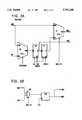
- FIG. 1shows an exemplary boundary scan cell.
- the boundary scan cellincludes multiplexers 2 and 4, and flip-flop elements 6 and 8.
- Datain the form of test data or instructions, is input to the first inputs of multiplexers 2 and 4 on line NDI, while the output of a previous boundary scan cell is input to the second input of multiplexer 2 on line SDI.
- the output of multiplexer 2is determined by a control signal on line SHIFT/LOAD
- the output of multiplexer 4is determined by a control signal on line MODE.
- the data sampled by flip-flop 6may be serially passed through to a successive boundary scan cell via scan data out line SDO, or may be supplied to flip-flop 8.
- Flip-flop 8is an intermediate storage element which samples and stores a value for use in a future test.
- Multiplexer 4receives normal data on line NDI at one input, and receives test data stored in flip-flop 8 at a second input.
- Multiplexer 4outputs data on line NDO under the control of the MODE signal.
- scan cellsare each connected to respective data pins of an integrated circuit, test data stored in the flip-flop 8 of each scan cell can be supplied to the data pins under the control of the MODE signal.
- Flip-flops 6 and 8operate according to separate clock signals A and B to enable flip-flop 8 to source the output of the boundary scan cell while new data is input to flip-flop 6.
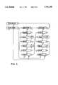
- boundary scan cells around a group of interconnected integrated circuits on a circuit boardis shown.
- the boundary scan cells around each integrated circuitform a shift register.
- This arrangementallows the interconnections between the circuit components in each of the integrated circuits to be tested by shifting test data into all of the boundary scan cells associated with integrated circuit output pins and loading input test data in parallel through the component interconnections into the cells associated with integrated circuit input pins.
- This arrangementalso allows the integrated circuits on the circuit board to be tested by isolating the internal logic circuitry of each chip from the surrounding circuit elements while an internal self-test is performed.
- the boundary scan cell methodalso permits a limited slow-speed static test of the internal logic circuitry of a chip by allowing test data to be input to the chip and the chip output data analyzed. Because the boundary scan register permits parallel loading of cells at both the input and output pins of an integrated circuit and permits the shifting out of the results, the register effectively samples data flowing through a component without interfering with the operation of the component. While boundary scan cells offer numerous benefits, a functional test of the operation of the complete system of interconnected integrated circuits requires separate automatic test equipment (ATE) or a system-level self test.
- ATEautomatic test equipment
- a built-in self test (BIST) architecturetypically includes a pattern or operand generator for producing test operands, each of which is applied to the internal logic circuitry of the integrated circuit. The results of each test operand are compressed into a "signature" which is compared to predetermined signatures to detect faults.
- BIST architectureis advantageous because the test circuitry is fabricated on the chip with the main logic functions, while having a minimal impact on the main logic functions. Further, since the test results are processed by BIST circuitry, the number of tasks which must be performed by external components is reduced, and maintenance software is simplified. BIST also allows for testing at full system clock rates, significantly reducing test time. BIST further allows for testing any number of different types of circuits, independent of specific chip logic functions, at the wafer, chip, or system levels, both before and after assembly into a computer.
- BIST architectureshave limitations.
- BIST architecturesrequire a means for selecting a system clock for normal operations and a test clock for test operations.
- a clock multiplexeris provided in each integrated circuit having a BIST capability. Examples of such architectures include U.S. Pat. No. 4,701,920 to Resnick et al. and U.S. Pat. No. 5,138,619 to Fasang et al. In such an arrangement, there are significant and variable delays in the clock distribution circuitry. Because different clock multiplexers are used for each integrated circuit in a system, the clock signals supplied to the different circuits may have varying phases (skew). Further, many known BIST architectures include customized interfaces, which often require an increase in the number of input or output pins needed to fabricate the integrated circuit.
- a BIST architectureit would be advantageous for a BIST architecture to include an industry standardized, low pin-count interface. It would also be advantageous for a BIST architecture to allow the testing using either known, externally supplied test data or pseudo-random test data patterns generated on the chip. It would further be advantageous for a BIST architecture to eliminate the need for an on-chip clock multiplexer to allow the main integrated circuits to operate at a high speed, while allowing the test circuitry to operate at a lower speed, and avoiding significant and variable clock delays and skews.
- the present inventionprovides for a fast BIST architecture which incorporates a standard, low pin-count interface, a single external clock multiplexer for testing multiple integrated circuits, and which allows testing to be performed using either internally or externally generated test data.
- a BIST circuitis capable of both boundary scan testing as well as internal scan testing of the internal logic circuitry of the integrated circuit.
- the BIST architecture according to the present inventionmay include a built-in pseudo-random pattern generator for generating test data patterns for input into one or more boundary scan registers or one or more internal scan registers. A testing operation may be performed using either the internally-generated pseudo-random test data or test data supplied from an external source.
- a testing operationmay be initiated by a control signal from an external controller.
- the control signalis received by an interface on the integrated circuit, which generates instructions in response to the control signal.
- the instructions generated by the control signalare decoded and used to control the scan cells of the boundary scan registers and internal scan registers, which sample and shift test data according to a test clock signal.
- Output test datamay be compressed in a signature compression means to form a data signature which is compared to a predetermined signature to detect faults. It is presently preferred that the interface be compatible with IEEE standard 1149.1.
- a single external clock multiplexerfor selectively interrupting the supply of the system clock signal to all of the integrated circuits to be tested during the sampling and shifting of data.
- the clock multiplexerenables the internal circuitry of the integrated circuit to generate output test data from the input test data stored in the scan registers using the system clock, and enables the sampling and shifting of data to be performed using the test clock.
- Input test datacan be loaded into the scan registers, shifted within the scan registers, or output by the scan registers while the system clock is interrupted.
- FIG. 1is a block diagram of a standard boundary scan cell known in the art
- FIG. 2shows a standard boundary scan test arrangement known in the art for a circuit board containing multiple integrated circuits
- FIG. 3Ais a block diagram of a boundary scan cell suitable for use in the present invention.
- FIG. 3Bis a block diagram of an internal scan cell suitable for use in the present invention.
- FIG. 4is a block diagram of an integrated circuit having a Built-In Self Test (BIST) architecture according to the present invention
- FIG. 5is a state diagram for the state machine used in the Interface of the BIST architecture of FIG. 4;
- FIG. 6shows a test arrangement for a system containing multiple integrated circuits having a BIST architecture according to the present invention.
- a scan cell suitable for use in the present inventionis shown.
- the cellmay be connected to an input pin or an output pin of an integrated circuit.
- input data from an external sourceis received on normal data in line NDI, and data is output from multiplexer M1 as input data to the integrated circuit pin on normal data out line NDO.
- output data from the output pinis received on normal data in line NDI, and data is output to a connection line (not shown) associated with the output pin on normal data out line NDO.
- a scan cell for performing a scan test of internal circuitryis shown in FIG. 3B.
- Such an internal scan cellincludes a single multiplexer M0 which receives data from the internal logic circuitry of the integrated circuit on line NDI.
- the multiplexer M0is controlled by normal/test select signal NRM -- TST, and selectively provides the data present on line NDI or the data sampled by previous stage flip-flop FF0 as output data on line NDO.
- the flip-flop FF0can be implemented by a component of the internal logic circuitry of the integrated circuit. Further, as shown in FIG. 3B, the flip-flop FF0 samples data according to a system clock signal CLK.
- each boundary scan cellpreferably includes a multiplexer M1, which is controlled by normal/test select signal NRM -- TST and which selectively provides the data present on line NDI or the data sampled by flip-flop FF1 as output data on line NDO.
- the cellalso includes multiplexer M0, which is controlled by shift/load signal SHIFT/LOAD, and which selectively provides the data present on line NDI or the data present on scan data in line SDI to be sampled by flip-flop FF0.
- the output of flip-flop FF0is supplied to scan data out line SDO, and also as the input to flip-flop FF1.
- the boundary scan cellreceives data sampled by the flip-flop FF1 of a previous scan cell on line SDI, and outputs data to the multiplexer M0 of a successive scan cell on line SDO.
- the flip-flops FF0 and FF1 shown in FIG. 3Asample data output by multiplexer M0 according to a test clock signal TCK.
- each boundary scan cell in FIG. 3Ais controlled by control signals SHIFT/LOAD, SCAN ENABLE, UPDATE, and NRM -- TST, which are supplied by an interface element of the integrated circuit in a manner to be described below.
- the control signalscause the multiplexer M1 to provide the data on normal data in line NDI to normal data out line NDO.
- input test datacan be provided to input data pins via lines NDI and NDO.
- the input test datacan be sampled by flip-flop FF0 based on the states of control signals SHIFT/LOAD and SCAN ENABLE.
- Data sampled by flip-flop FF0can be sampled by flip-flop FF1 or shifted to a successive boundary cell based on the states of control signals SCAN ENABLE and UPDATE.
- Data sampled by flip-flop FF1can be output on normal data out line NDO to the input pins of the integrated circuit based on the states of control signals UPDATE and NRM -- TST.
- Boundary cells connected to output pins of the integrated circuitmay be controlled in a similar manner to output sample or shift output test data.
- shiftand “shifting” are used herein to refer to the operation of shifting data between the cells of the scan registers or the operation of outputting data from the scan cells.
- the scan cellsare connected together to form a shift register.
- the scan cells associated with input pins or inputs to internal circuitry of the integrated circuitare serially loaded with test data received on normal data in line NDI, the internal circuitry of the integrated circuit operates for a predetermined time, and the output data is sampled by the scan cells. After a test operation is performed, the output test data is shifted out while a new vector of test data is loaded into the shift register.
- vectoris used herein to describe one set or pattern of input test data to be supplied to an integrated circuit for a test operation.
- the BIST systemincludes an interface 10, a test controller 12, a pseudo-random pattern generator 14, a pattern compressor 16, an internal scan register 18, a boundary scan register 20, and an output multiplexer 22.
- the interface 10is a test access port (TAP) interface, which is preferably compatible with IEEE standard 1149.1.
- IEEE standard 1149.1is a test access port and boundary scan architecture standard published by the Institute for Electrical and Electronic Engineers (IEEE), and defines circuitry that may be built into an integrated circuit to assist in the test, maintenance, and support of assembled printed circuit boards.
- the interface 10receives, from an external TAP control device (not shown), test data and instructions on line TDI, a test mode select signal on line TMS, and a test clock signal on line TCK.
- the TAP control deviceis an external element which may be a microprocessor or other suitable test control equipment known in the art.
- Interface 10includes a state machine which generates instructions in response to the test mode select signal on line TMS. The state machine controls the test operation, and will be described in more detail below.
- Interface 10also includes an instruction register for storing instructions generated by the state machine, an instruction register decoder for decoding the instructions, and a bypass register for bypassing the internal logic circuitry of the integrated circuit.
- Interface 10outputs a scan test start signal on line START, a reset control signal on line TLRST, boundary scan control signals on lines BSC (which include the SHIFT/HOLD, SCAN ENABLE, UPDATE, and NRM -- TST signals used to control the scan cells as shown in FIG. 3), and instruction register and bypass signals on lines IRB.
- Scan controller 12receives the signals on lines START, TLRST, and SHIFT/HOLD from interface 10, receives input test data and instructions on line TDI from the external TAP control device, and receives a system clock signal from an external source on line CLK.
- Scan controller 12includes a scan register length counter, an iteration counter, a state machine, and a command register.
- the iteration counterhas a count value which represents the number of test vectors to be used to test the integrated circuit
- the scan register length counterhas a count value which represents the number of elements (i.e., cells or stages) in the scan register to be selected for a given test operation.
- the count values of the scan register length counter and iteration countermay be fixed or programmable via data on line TDI; however, it will be appreciated that programmable count values allow greater flexibility in that separate tests using multiple scan registers or a single test using a single unified scan register can be readily performed.
- the countersare reset at the start of a scan test operation by a control signal on line TLRST, and the scan test operation terminates when both counters reach their terminal count values.
- the state machine included in scan controller 12is a four-state state machine for controlling the scan test operation.
- the command registeris a multiple bit register for storing commands. In the preferred embodiment, the command register is an eight-bit register, and each bit controls one of the group of multiplexers as shown in FIG. 4 on multiplexer control line MC to control the operation of the system.
- the control signals on lines BSC and MCare supplied as inputs to multiplexer 11, which is controlled by a separate multiplexer control signal supplied from scan controller 12.
- a scan test operationis initiated by a scan test start signal received by the scan controller 12 from interface 10 on line START, and when the scan test operation is completed (i.e., when the scan register length counter and iteration counter reach their terminal count values), the scan controller 12 informs interface 10 via a status bit on line DONE.
- test datais supplied to internal scan register 18 and boundary scan register 20 from either test data in line TDI or from pattern generator 14, depending upon the state of the control signal input to multiplexer 31.
- Multiplexer 31thus enables the integrated circuit to be tested using test data generated by the external TAP control device, which typically includes predetermined data patterns, or pseudo-random test data generated by pattern generator 14.
- scan controller 12When it is desired to supply pseudo-random test data to the test circuitry, scan controller 12 causes pattern generator 14 to generate the pseudo-random test signal patterns, and generates the control signal to cause multiplexer 31 to supply the pseudo-random test signal patterns to scan registers 18 and/or 20. When it is desired to supply known or predetermined test signal patterns to the test circuitry, scan controller 12 causes multiplexer 31 to supply data on line TDI to the scan registers 18 and/or 20. It will be appreciated that a scan test may be performed using one or more boundary scan registers 20, one or more internal scan registers 18, or a concatenation of internal scan register 18 and boundary scan register 20.
- the scan cells of the selected scan chain or chains associated with input pins or input internal circuitry elementsare serially loaded with input test data from either test data in line TDI or pattern generator 14 on the normal data in line NDI of the scan cell.
- the loading of the boundary scan cellsis performed according to the test clock TCK, while the loading of the internal scan cells is performed according to the system clock CLK.
- the input test datais then supplied in parallel to the internal circuitry for a predetermined time (e.g., one system clock pulse), and the output test data is sampled by the cells of the selected scan chain or chains associated with output pins or output elements of the internal circuitry.
- the output test datais shifted out while a new vector of input test data is loaded into the selected scan chain or chains.
- the shifting of the output test datais performed according to the test clock TCK for the boundary scan register, and according to the system clock CLK for the internal scan register.
- the output test datais supplied to pattern compressor 16, which compresses the output test data into a signature for comparison with a predetermined signature to determine if any faults are present in the tested circuitry.
- the comparison functionmay be performed by pattern compressor 16 or by a separate signature comparator or comparison element located on the integrated circuit or located external to all of the integrated circuits.
- Pattern generator 14generates pseudo-random test data patterns for input to the scan registers 18 and 20.
- Pattern generator 14is preferably a programmable type-2 linear feedback shift register (LFSR), which has a coefficient register and a seed.
- LFSRlinear feedback shift register
- a linear feedback shift registermay be characterized as a non-sequential repeating counter in which a coefficient register value determines the feedback characteristics of the register and the seed value determines the patterns which will be generated by the register.
- the seed value and coefficient register valuemay be programmable by the scan controller 12 using data supplied on test data-in line TDI, or may have fixed values. Pattern generator 14 operates according to the system clock CLK.
- Pattern compressor 16is, like the pattern generator 14, preferably a programmable type-2 linear feedback register having a seed and coefficient register which may be programmable or fixed.
- the output test data of the selected scan chainis input to pattern compressor 16.
- Pattern compressor 16generates a unique signature based on the serial data pattern received from the selected scan chain, the coefficient, and the starting seed value. Pattern compressor 16 operates according to system clock CLK.
- scan controller 12, pattern generator 14, and pattern compressor 14may be implemented as a single data register which may be loaded by the interface 10 or by data on line TDI.
- Internal scan register 18is comprised of flip-flops in the existing logic circuitry of the integrated circuit.
- the flip-flops in the internal integrated circuitryhave a 2:1 multiplex ratio in which a first input is a normal functional signal (i.e., a test signal or data signal), a second input is from a prior internal scan chain element, and the multiplexer select input is controlled by scan controller 12 using the control signals SHIFT/LOAD, SCAN ENABLE, UPDATE, and NRM -- TST.
- SHIFT/LOADnormal functional signal
- SCAN ENABLEi.e., a test signal or data signal
- the internal scan register 18operates according to system clock signal CLK.
- Boundary scan register 20is comprised of boundary scan cells, such as those shown in FIG. 3, which are connected in the manner shown in FIG. 2. As shown in FIG. 4, the boundary scan register 20 operates according to test clock TCK. The individual boundary scan cells are controlled by the signals SHIFT/LOAD, SCAN ENABLE, UPDATE, and NRM -- TST on lines BSC. It will be appreciated that, to maximize fault detection capabilities, both the boundary scan register 20 and the internal scan register 18 can be selected for testing by controller 12. When both the boundary scan register 20 and the internal scan register 18 are selected, they are concatenated together through multiplexer 30 to form the equivalent of a single register. To ensure that the data in the final cell of internal scan register 18 is successfully shifted into the first cell of boundary scan register 20, the concatenated registers should be clocked by the same clock signal, preferably test clock TCK.
- Boundary scan register 20in addition to supplying and receiving responses to input test data, may also be configured to provide a device identification function.
- the last cells of the boundary scan registerprovide a dual function of either storing the device ID or storing normal scan register information. This implementation is possible because there is never a case in which both scan data and device identification information will be required simultaneously.
- a separate device ID registermay be provided; however, the use of dual function boundary scan cells reduces the number of gates required to implement the device identification function.
- the device IDis provided as an input to output multiplexer 22 on line DEVICE ID.
- the output test data from internal scan register 18 and boundary scan register 20are supplied as separate inputs or as a single input to multiplexer 32, the output of which is determined by one of the bits in the command register of controller 12.
- the output of multiplexer 32sampled by D-type flip-flop 34 on a pulse of system clock CLK, and is provided to pattern compressor 16 through multiplexers 36 and 38.
- pattern compressor 16compresses the outputs of internal scan register 18 and boundary scan register 20 to form a unique signature.
- the output of multiplexer 32 and the signature output of pattern compressor 16are both provided as inputs to multiplexer 39, the output of which is determined by a command register bit from controller 12.
- the output of multiplexer 39is supplied as one input to output multiplexer 22. As described above, the multiplexers are controlled by individual bits of the command register contained in scan controller 12.
- test data or instructions on line TDI interface 10can provide a RAM BIST control signal to control the operation of RAM BIST circuit.
- the RAM BIST circuitreceives the test clock signal on line TCK and the test data or instructions on line TDI, and provides an output signal to output multiplexer 22.
- Output multiplexer 22may receive inputs from the following sources: the instruction register and bypass register contained within interface 10 on lines IRB, boundary scan register 20, device identification line DEVICE ID, RAM BIST element 40, internal scan register 18, and a pattern compressor 16. The specific inputs received by output multiplexer 22 and the output signal provided by output multiplexer 22 are determined by the control signals on lines BSC and MC. Output multiplexer 22 is clocked according to test clock TCK.
- the output of multiplexer 22 on line TDOis present only during an active access operation to interface 10. Since interface 10 is not typically accessed during a test operation, line TDO will not be driven during a test operation. Since it may be desirable to view the output test data during a test session, there is provided a SCANOUT output from multiplexer 38.
- the SCANOUT outputenables signature comparison to be performed by a comparator located external to the integrated circuits.
- an exemplary state transition diagram for the state machine 50 contained in interface 10is shown.
- the annotations next to the flow arrowsindicate the value of the test mode select signal on line TMS.
- an initial test logic or reset state 0may be achieved by holding the test mode select signal high for a minimum of five cycles of test clock TCK. From state 0, if the test mode select signal is maintained high, the state machine will idle at state 0, and if the test mode select signal goes low, the state machine enters a RunTest/Idle state 1, in which built-in test routines may be executed. If no built-in test routines are available, then state 1 is a null state.
- the test mode select signalcan be used to force a transition into data register scan state 2, from which data in the scan elements comprising either the internal scan register 18 or boundary scan register 20 can be captured, shifted, paused; or shifted to the secondary flip-flops in each cell (updated) in states 2-8.
- the test mode select signalcan be used to enter an instruction register manipulation path comprised of states 9-15 to manipulate data in the instruction register of interface 10.
- boundary scan status(which may be, for example, a current instruction or a flag indicating the result of a completed test) can be captured in state 10, a new boundary scan instruction may be loaded in state 15, or the instruction register data can be shifted, paused, or unaffected in states 11-14.
- FIG. 5is merely exemplary, and that many other state transition schemes may be implemented in the BIST architecture according to the present invention.
- the IEEE standard 1149.1 reference described abovesuggests an alternative state transition scheme which may allow a reduced gate count.
- interface 10includes state machine 50, which receives test mode select line TMS, test reset line TRST, and test clock line TCK.
- State machine 50outputs data manipulation signals to instruction register 52 and to the scan registers 18 and 20 as described above with respect to FIG. 5.
- the data manipulation signalscontrol the scan paths, which include the paths associated with the bypass register 54, internal scan registers 18, boundary scan register 20, and instruction register 52.
- Bypass register 54is a single flip-flop register which provides a direct, synchronized conduit through the integrated circuit when no interaction with the integrated circuit is desired.
- Test datais input through line TDI to the SDI (scan data in, see FIG. 3) input of the first boundary scan cell in each scan path.
- the SDO(scan data out, see FIG. 3) signal from the last scan cell of each scan path register is connected to the multiplexers that lead to output multiplexer 22 and test data out line TDO.
- Instruction register 52stores instructions from state machine 50 and determines the test to be performed or the test data register for future data scan operations.
- the instructions stored in instruction register 52are decoded by instruction decoder 56 for execution by the elements receiving boundary scan control signals on line BSC. That is, the decoded instructions cause appropriate signals to be applied to lines SHIFT/HOLD, SCAN ENABLE, UPDATE, and NRM -- TST of control lines BSC to control the operation of the scan cells as shown in FIG. 3. All instructions are executed during the Run-Test Idle state 1 of the state machine 50.
- IEEE standard 1149.1provides for BYPASS, SAMPLE/PRELOAD, and EXTEST instructions.
- the BYPASS instructionis implemented when instruction register 52 contains all 1's, and causes all future data transfers to pass through the single flip-flop bypass register 54. This instruction allows the test programmer to quickly move input test data sets through devices which are not relevant to the test.
- the SAMPLE/PRELOAD instructionis implemented by a user-defined code and causes current integrated circuit data to be sampled on the rising edge of test clock TCK during capture state 3 of state machine 50. This instruction also causes data in each scan register to be transferred to the secondary flip-flop of each register cell on the falling edge of test clock TCK during the update state 8 of state machine 50.
- the EXTEST instructionis implemented when the instruction register contains all 0's, and causes data in the boundary scan register to be driven on the integrated circuit output pin on the falling edge of test clock TCK during the update state 8 of state machine 50. This instruction also causes all data on the integrated circuit input pins to be sampled on the rising edge of test clock TCK during capture state 3 of state machine 50.
- IEEE standard 1149.1also recommends implementation of INTEST and RUNBIST instructions.
- INTESTcauses all inputs to the chip and all outputs driven off the chip to be captured, and substitutes the boundary scan data for the system data on all outputs.
- RUNBISTcauses the chip to perform a self-test operation. It will be appreciated that the instruction register codes for implementing these instructions, as well as for the BYPASS, SAMPLE/PRELOAD, and EXTEST instructions may be defined by the user.
- each integrated circuit IC 1 , IC 2 , . . . IC nhas a BIST architecture according to the present invention as described above.
- BIST architecturesrequire a clock multiplexer which allows the test clock or a system clock to be used as the active clock signal.
- a clock multiplexer 70is provided at a location external to all of the integrated circuits to be tested.
- the multiplexer 70allows the system clock CLK to be replaced by the test clock TCK on each one of the integrated circuits IC 1 , IC 2 , . . . IC n , based on the state of a signal on line RUN -- TEST from the external TAP control device (not shown).
- the operations of loading, shifting, and sampling of test datamay be performed according to the test clock.
- the system clockmay be supplied to the circuit or circuits to be tested to enable at-speed internal testing to be performed. By conducting tests according to the faster system clock, several thousand serial pseudo-random test patterns can be used to test the circuits in a relatively short time.
- the signaturemay be read out through output multiplexer 22 according to the test clock replacing the system clock to the integrated circuits.
- the system clockis supplied to the integrated circuits through multiplexer 70. Because the clock multiplexer 70 is provided at a point external to the circuits to be tested, the present invention eliminates the need for separate clock multiplexers provided in each device, thereby eliminating the significant and variable clock delays associated with multiple clock multiplexers and enhancing the performance of the functional circuitry. Further, because all of the devices to be tested receive the same clock signal, clock phase delays are transparent to the system.
Landscapes
- Engineering & Computer Science (AREA)
- General Engineering & Computer Science (AREA)
- Physics & Mathematics (AREA)
- General Physics & Mathematics (AREA)
- Tests Of Electronic Circuits (AREA)
- Test And Diagnosis Of Digital Computers (AREA)
Abstract
Description
Claims (22)
Priority Applications (2)
| Application Number | Priority Date | Filing Date | Title |
|---|---|---|---|
| US08/739,426US5701308A (en) | 1996-10-29 | 1996-10-29 | Fast bist architecture with flexible standard interface |
| US08/915,632US5872793A (en) | 1996-10-29 | 1997-08-21 | Fast bist architecture with flexible standard interface |
Applications Claiming Priority (1)
| Application Number | Priority Date | Filing Date | Title |
|---|---|---|---|
| US08/739,426US5701308A (en) | 1996-10-29 | 1996-10-29 | Fast bist architecture with flexible standard interface |
Related Child Applications (1)
| Application Number | Title | Priority Date | Filing Date |
|---|---|---|---|
| US08/915,632ContinuationUS5872793A (en) | 1996-10-29 | 1997-08-21 | Fast bist architecture with flexible standard interface |
Publications (1)
| Publication Number | Publication Date |
|---|---|
| US5701308Atrue US5701308A (en) | 1997-12-23 |
Family
ID=24972259
Family Applications (2)
| Application Number | Title | Priority Date | Filing Date |
|---|---|---|---|
| US08/739,426Expired - LifetimeUS5701308A (en) | 1996-10-29 | 1996-10-29 | Fast bist architecture with flexible standard interface |
| US08/915,632Expired - LifetimeUS5872793A (en) | 1996-10-29 | 1997-08-21 | Fast bist architecture with flexible standard interface |
Family Applications After (1)
| Application Number | Title | Priority Date | Filing Date |
|---|---|---|---|
| US08/915,632Expired - LifetimeUS5872793A (en) | 1996-10-29 | 1997-08-21 | Fast bist architecture with flexible standard interface |
Country Status (1)
| Country | Link |
|---|---|
| US (2) | US5701308A (en) |
Cited By (45)
| Publication number | Priority date | Publication date | Assignee | Title |
|---|---|---|---|---|
| US5822228A (en)* | 1997-05-27 | 1998-10-13 | Lsi Logic Corporation | Method for using built in self test to characterize input-to-output delay time of embedded cores and other integrated circuits |
| US5900753A (en)* | 1997-03-28 | 1999-05-04 | Logicvision, Inc. | Asynchronous interface |
| US5909404A (en)* | 1998-03-27 | 1999-06-01 | Lsi Logic Corporation | Refresh sampling built-in self test and repair circuit |
| US5953285A (en)* | 1997-09-17 | 1999-09-14 | Cypress Semiconductor Corp. | Scan path circuitry including an output register having a flow through mode |
| US6006347A (en)* | 1997-09-17 | 1999-12-21 | Cypress Semiconductor Corporation | Test mode features for synchronous pipelined memories |
| US6079039A (en)* | 1996-12-25 | 2000-06-20 | Nec Corporation | Test circuit and test method for testing semiconductor chip |
| US6240537B1 (en)* | 1997-09-08 | 2001-05-29 | Samsung Electronics Co., Ltd. | Signature compression circuit and method |
| US20010037480A1 (en)* | 2000-04-28 | 2001-11-01 | Whetsel Lee D. | Dual mode test access port method and apparatus |
| US20010037479A1 (en)* | 2000-04-28 | 2001-11-01 | Whetsel Lee D. | Selectable dual mode test access port method and apparatus |
| US6357026B1 (en)* | 1999-01-05 | 2002-03-12 | The Boeing Company | System and method for at-speed interconnect tests |
| US20020040456A1 (en)* | 2000-09-29 | 2002-04-04 | Aditya Mukherjee | Partially distributed control mechanism for scanout incorporating flexible debug triggering |
| US20030131298A1 (en)* | 1999-11-23 | 2003-07-10 | Mentor Graphics Corporation | Test pattern compression for an integrated circuit test environment |
| US6708303B1 (en)* | 1998-03-06 | 2004-03-16 | Texas Instruments Incorporated | Method and apparatus for controlling a seperate scan output of a scan circuit |
| US6708305B1 (en) | 2000-10-18 | 2004-03-16 | International Business Machines Corporation | Deterministic random LBIST |
| US20040133825A1 (en)* | 2002-11-08 | 2004-07-08 | Matsushita Electric Industrial Co., Ltd | Path delay measuring circuitry |
| US20040187059A1 (en)* | 2000-01-10 | 2004-09-23 | Whetsel Lee D. | Boundary scan path method and system with functional and non-functional scan cell memories |
| US20040230884A1 (en)* | 2003-02-13 | 2004-11-18 | Janusz Rajski | Compressing test responses using a compactor |
| US6886122B1 (en)* | 1999-03-08 | 2005-04-26 | France Telecom | Method for testing integrated circuits with memory element access |
| US20050188290A1 (en)* | 2004-02-19 | 2005-08-25 | International Business Machines Corporation | Method and structure for picosecond-imaging-circuit-analysis based built-in-self-test diagnostic |
| US20060041812A1 (en)* | 2003-02-13 | 2006-02-23 | Janusz Rajski | Fault diagnosis of compressed test responses |
| US20060041813A1 (en)* | 2003-02-13 | 2006-02-23 | Janusz Rajski | Adaptive fault diagnosis of compressed test responses |
| US20060041814A1 (en)* | 2003-02-13 | 2006-02-23 | Janusz Rajski | Fault diagnosis of compressed test responses having one or more unknown states |
| US7093175B2 (en) | 1999-11-23 | 2006-08-15 | Janusz Rajski | Decompressor/PRPG for applying pseudo-random and deterministic test patterns |
| US20070011535A1 (en)* | 2004-03-29 | 2007-01-11 | Kenichi Anzou | Semiconductor integrated circuit |
| US7260591B2 (en) | 1999-11-23 | 2007-08-21 | Janusz Rajski | Method for synthesizing linear finite state machines |
| US7263641B2 (en) | 1999-11-23 | 2007-08-28 | Janusz Rajski | Phase shifter with reduced linear dependency |
| US20080077836A1 (en)* | 2006-09-27 | 2008-03-27 | Khoche A Jay | Diagnostic Information Capture from Memory Devices with Built-in Self Test |
| CN100388215C (en)* | 2005-01-14 | 2008-05-14 | 威盛电子股份有限公司 | Debug Support Unit and Debug Method Using Multiple Asynchronous Clocks on Chip Hardware |
| US7478296B2 (en)* | 1999-11-23 | 2009-01-13 | Janusz Rajski | Continuous application and decompression of test patterns to a circuit-under-test |
| US7480843B1 (en)* | 2004-09-29 | 2009-01-20 | Xilinx, Inc. | Configuration access from a boundary-scannable device |
| US7493540B1 (en) | 1999-11-23 | 2009-02-17 | Jansuz Rajski | Continuous application and decompression of test patterns to a circuit-under-test |
| US7500163B2 (en) | 1999-11-23 | 2009-03-03 | Janusz Rajski | Method and apparatus for selectively compacting test responses |
| US7506210B1 (en) | 2003-06-26 | 2009-03-17 | Xilinx, Inc. | Method of debugging PLD configuration using boundary scan |
| US20090183042A1 (en)* | 2000-03-09 | 2009-07-16 | Texas Instruments Incorporated | Adapting scan-bist architectures for low power operation |
| US8438441B2 (en)* | 1998-02-10 | 2013-05-07 | Texas Instruments Incorporated | Tap with three multiplexers and port enable control output |
| US8533547B2 (en) | 1999-11-23 | 2013-09-10 | Mentor Graphics Corporation | Continuous application and decompression of test patterns and selective compaction of test responses |
| US9134370B2 (en) | 1999-11-23 | 2015-09-15 | Mentor Graphics Corporation | Continuous application and decompression of test patterns and selective compaction of test responses |
| CN105823978A (en)* | 2016-03-11 | 2016-08-03 | 福州瑞芯微电子股份有限公司 | Universal chip testing clock circuit and testing method thereof |
| US9664739B2 (en) | 1999-11-23 | 2017-05-30 | Mentor Graphics Corporation | Continuous application and decompression of test patterns and selective compaction of test responses |
| US20170160340A1 (en)* | 2014-08-15 | 2017-06-08 | Huawei Technologies Co., Ltd. | Test apparatus and testable asynchronous circuit |
| CN111880073A (en)* | 2020-06-28 | 2020-11-03 | 北京旋极信息技术股份有限公司 | Built-in test design method and system |
| US11073558B2 (en)* | 2018-12-05 | 2021-07-27 | Realtek Semiconductor Corp. | Circuit having multiple scan modes for testing |
| WO2022088594A1 (en)* | 2020-10-28 | 2022-05-05 | 深圳市紫光同创电子有限公司 | Boundary scan test method and storage medium |
| US20220358270A1 (en)* | 2021-05-08 | 2022-11-10 | Realtek Semiconductor Corp. | Chip verification system and verification method therefor |
| CN115356620A (en)* | 2022-08-17 | 2022-11-18 | 地平线(上海)人工智能技术有限公司 | Digital logic self-test method, device, electronic equipment and medium of system on chip |
Families Citing this family (32)
| Publication number | Priority date | Publication date | Assignee | Title |
|---|---|---|---|---|
| JP3039362B2 (en)* | 1996-03-28 | 2000-05-08 | 日本電気株式会社 | Method for creating test pattern of semiconductor integrated logic circuit |
| US6141790A (en)* | 1997-10-30 | 2000-10-31 | Synopsys, Inc. | Instructions signature and primary input and primary output extraction within an IEEE 1149.1 compliance checker |
| US6023778A (en)* | 1997-12-12 | 2000-02-08 | Intel Corporation | Method and apparatus for utilizing mux scan flip-flops to test speed related defects by delaying an active to inactive transition of a scan mode signal |
| US6128758A (en)* | 1998-05-20 | 2000-10-03 | National Semiconductor Corporation | Modular re-useable bus architecture |
| US7036060B2 (en)* | 1998-09-22 | 2006-04-25 | Hitachi, Ltd. | Semiconductor integrated circuit and its analyzing method |
| JP2000266815A (en)* | 1999-03-16 | 2000-09-29 | Mitsubishi Electric Corp | Electronic system with self-diagnosis function and electronic system simulation device |
| US6456101B2 (en) | 1999-04-07 | 2002-09-24 | Agere Systems Guardian Corp. | Chip-on-chip testing using BIST |
| DE19917884C1 (en) | 1999-04-20 | 2000-11-16 | Siemens Ag | Circuit with built-in self-test |
| EP1083682A3 (en)* | 1999-09-10 | 2003-07-02 | TRW Inc. | Built-in self test (BIST) approach for regenerative data transmission system |
| EP1475643B1 (en)* | 1999-11-23 | 2006-09-20 | Mentor Graphics Corporation | Test pattern compression for an integrated circuit test environment |
| US6484275B1 (en)* | 1999-11-26 | 2002-11-19 | Hewlett-Packard Company | System and method for interfacing data with a test access port of a processor |
| JP2001255356A (en)* | 2000-03-08 | 2001-09-21 | Matsushita Electric Ind Co Ltd | Test pattern generation method and test method for semiconductor integrated circuit |
| US6618827B1 (en)* | 2000-04-13 | 2003-09-09 | Hewlett-Packard Development Company, L.P. | System and method for parallel testing of IEEE 1149.1 compliant integrated circuits |
| US6591388B1 (en) | 2000-04-18 | 2003-07-08 | International Business Machines Corporation | High speed sink/source register to reduce level sensitive scan design test time |
| DE10041137A1 (en)* | 2000-08-21 | 2002-03-21 | Philips Corp Intellectual Pty | Arrangement for testing integrated circuits |
| US6587982B1 (en)* | 2000-09-05 | 2003-07-01 | Advanced Micro Devices, Inc. | Method of micro-architectural implementation of interface between bist state machine and tester interface to enable bist cycling |
| US20020095633A1 (en)* | 2000-10-05 | 2002-07-18 | Ulf Pillkahn | Electronic component, a test configuration and a method for testing connections of electronic components on a printed circuit board |
| US7073110B1 (en)* | 2002-04-26 | 2006-07-04 | Xilinx, Inc. | Method and system for programmable boundary-scan instruction register |
| US7412639B2 (en)* | 2002-05-24 | 2008-08-12 | Verigy (Singapore) Pte. Ltd. | System and method for testing circuitry on a wafer |
| US7149640B2 (en)* | 2002-06-21 | 2006-12-12 | King Tiger Technology, Inc. | Method and system for test data capture and compression for electronic device analysis |
| DE60313860D1 (en)* | 2003-06-24 | 2007-06-28 | St Microelectronics Srl | Integrated circuit with improved BIST circuit for performing a structured test |
| US7240267B2 (en)* | 2004-11-08 | 2007-07-03 | Marvell International Ltd. | System and method for conducting BIST operations |
| KR100622128B1 (en)* | 2004-12-17 | 2006-09-19 | 한국전자통신연구원 | Parallelism Shrink Key Generator |
| US7607057B2 (en)* | 2004-12-28 | 2009-10-20 | Lsi Corporation | Test wrapper including integrated scan chain for testing embedded hard macro in an integrated circuit chip |
| US7487419B2 (en)* | 2005-06-15 | 2009-02-03 | Nilanjan Mukherjee | Reduced-pin-count-testing architectures for applying test patterns |
| US7804724B2 (en)* | 2007-05-02 | 2010-09-28 | Alcatel Lucent | Method and apparatus for boundary scan programming of memory devices |
| US7685484B2 (en)* | 2007-11-14 | 2010-03-23 | International Business Machines Corporation | Methods for the support of JTAG for source synchronous interfaces |
| US8046651B2 (en) | 2008-04-02 | 2011-10-25 | Texas Instruments Incorporated | Compare circuit receiving scan register and inverted clock flip-flop data |
| US20110298490A1 (en)* | 2010-06-08 | 2011-12-08 | Alan Scott Hearn | Asymmetrical aging control system |
| KR20120120798A (en)* | 2011-04-25 | 2012-11-02 | 에스케이하이닉스 주식회사 | Memory and test method for memory |
| US8726108B2 (en)* | 2012-01-12 | 2014-05-13 | Lsi Corporation | Scan test circuitry configured for bypassing selected segments of a multi-segment scan chain |
| US9753087B2 (en)* | 2012-05-10 | 2017-09-05 | Telefonaktiebolaget Lm Ericsson (Publ) | Method for testing a multi-chip system or a single chip and system thereof |
Citations (11)
| Publication number | Priority date | Publication date | Assignee | Title |
|---|---|---|---|---|
| US4433413A (en)* | 1981-10-22 | 1984-02-21 | Siemens Corporation | Built-in apparatus and method for testing a microprocessor system |
| US4701920A (en)* | 1985-11-08 | 1987-10-20 | Eta Systems, Inc. | Built-in self-test system for VLSI circuit chips |
| US4724380A (en)* | 1984-12-21 | 1988-02-09 | Plessey Overseas Limited | Integrated circuit having a built-in self test design |
| US5051996A (en)* | 1989-03-27 | 1991-09-24 | The United States Of America As Represented By The United States Department Of Energy | Built-in-test by signature inspection (bitsi) |
| US5138619A (en)* | 1990-02-15 | 1992-08-11 | National Semiconductor Corporation | Built-in self test for integrated circuit memory |
| US5164665A (en)* | 1990-08-21 | 1992-11-17 | Mitsubishi Denki Kabushiki Kaisha | IC tester |
| US5184067A (en)* | 1988-07-12 | 1993-02-02 | Kabushiki Kaisha Toshiba | Signature compression circuit |
| US5230000A (en)* | 1991-04-25 | 1993-07-20 | At&T Bell Laboratories | Built-in self-test (bist) circuit |
| US5258985A (en)* | 1991-11-12 | 1993-11-02 | Motorola, Inc. | Combinational data generator and analyzer for built-in self test |
| US5301199A (en)* | 1991-12-16 | 1994-04-05 | Nippon Telegraph And Telephone Corporation | Built-in self test circuit |
| US5355369A (en)* | 1991-04-26 | 1994-10-11 | At&T Bell Laboratories | High-speed integrated circuit testing with JTAG |
- 1996
- 1996-10-29USUS08/739,426patent/US5701308A/ennot_activeExpired - Lifetime
- 1997
- 1997-08-21USUS08/915,632patent/US5872793A/ennot_activeExpired - Lifetime
Patent Citations (11)
| Publication number | Priority date | Publication date | Assignee | Title |
|---|---|---|---|---|
| US4433413A (en)* | 1981-10-22 | 1984-02-21 | Siemens Corporation | Built-in apparatus and method for testing a microprocessor system |
| US4724380A (en)* | 1984-12-21 | 1988-02-09 | Plessey Overseas Limited | Integrated circuit having a built-in self test design |
| US4701920A (en)* | 1985-11-08 | 1987-10-20 | Eta Systems, Inc. | Built-in self-test system for VLSI circuit chips |
| US5184067A (en)* | 1988-07-12 | 1993-02-02 | Kabushiki Kaisha Toshiba | Signature compression circuit |
| US5051996A (en)* | 1989-03-27 | 1991-09-24 | The United States Of America As Represented By The United States Department Of Energy | Built-in-test by signature inspection (bitsi) |
| US5138619A (en)* | 1990-02-15 | 1992-08-11 | National Semiconductor Corporation | Built-in self test for integrated circuit memory |
| US5164665A (en)* | 1990-08-21 | 1992-11-17 | Mitsubishi Denki Kabushiki Kaisha | IC tester |
| US5230000A (en)* | 1991-04-25 | 1993-07-20 | At&T Bell Laboratories | Built-in self-test (bist) circuit |
| US5355369A (en)* | 1991-04-26 | 1994-10-11 | At&T Bell Laboratories | High-speed integrated circuit testing with JTAG |
| US5258985A (en)* | 1991-11-12 | 1993-11-02 | Motorola, Inc. | Combinational data generator and analyzer for built-in self test |
| US5301199A (en)* | 1991-12-16 | 1994-04-05 | Nippon Telegraph And Telephone Corporation | Built-in self test circuit |
Cited By (105)
| Publication number | Priority date | Publication date | Assignee | Title |
|---|---|---|---|---|
| US6079039A (en)* | 1996-12-25 | 2000-06-20 | Nec Corporation | Test circuit and test method for testing semiconductor chip |
| US5900753A (en)* | 1997-03-28 | 1999-05-04 | Logicvision, Inc. | Asynchronous interface |
| US5822228A (en)* | 1997-05-27 | 1998-10-13 | Lsi Logic Corporation | Method for using built in self test to characterize input-to-output delay time of embedded cores and other integrated circuits |
| US6240537B1 (en)* | 1997-09-08 | 2001-05-29 | Samsung Electronics Co., Ltd. | Signature compression circuit and method |
| US5953285A (en)* | 1997-09-17 | 1999-09-14 | Cypress Semiconductor Corp. | Scan path circuitry including an output register having a flow through mode |
| US6006347A (en)* | 1997-09-17 | 1999-12-21 | Cypress Semiconductor Corporation | Test mode features for synchronous pipelined memories |
| US8438441B2 (en)* | 1998-02-10 | 2013-05-07 | Texas Instruments Incorporated | Tap with three multiplexers and port enable control output |
| US6708303B1 (en)* | 1998-03-06 | 2004-03-16 | Texas Instruments Incorporated | Method and apparatus for controlling a seperate scan output of a scan circuit |
| US5909404A (en)* | 1998-03-27 | 1999-06-01 | Lsi Logic Corporation | Refresh sampling built-in self test and repair circuit |
| US6357026B1 (en)* | 1999-01-05 | 2002-03-12 | The Boeing Company | System and method for at-speed interconnect tests |
| US6886122B1 (en)* | 1999-03-08 | 2005-04-26 | France Telecom | Method for testing integrated circuits with memory element access |
| US7805651B2 (en) | 1999-11-23 | 2010-09-28 | Mentor Graphics Corporation | Phase shifter with reduced linear dependency |
| US7900104B2 (en) | 1999-11-23 | 2011-03-01 | Mentor Graphics Corporation | Test pattern compression for an integrated circuit test environment |
| US9134370B2 (en) | 1999-11-23 | 2015-09-15 | Mentor Graphics Corporation | Continuous application and decompression of test patterns and selective compaction of test responses |
| US8533547B2 (en) | 1999-11-23 | 2013-09-10 | Mentor Graphics Corporation | Continuous application and decompression of test patterns and selective compaction of test responses |
| US7509546B2 (en) | 1999-11-23 | 2009-03-24 | Janusz Rajski | Test pattern compression for an integrated circuit test environment |
| US7500163B2 (en) | 1999-11-23 | 2009-03-03 | Janusz Rajski | Method and apparatus for selectively compacting test responses |
| US9664739B2 (en) | 1999-11-23 | 2017-05-30 | Mentor Graphics Corporation | Continuous application and decompression of test patterns and selective compaction of test responses |
| US10234506B2 (en) | 1999-11-23 | 2019-03-19 | Mentor Graphics Corporation | Continuous application and decompression of test patterns and selective compaction of test responses |
| US7493540B1 (en) | 1999-11-23 | 2009-02-17 | Jansuz Rajski | Continuous application and decompression of test patterns to a circuit-under-test |
| US8108743B2 (en) | 1999-11-23 | 2012-01-31 | Mentor Graphics Corporation | Method and apparatus for selectively compacting test responses |
| US8024387B2 (en) | 1999-11-23 | 2011-09-20 | Mentor Graphics Corporation | Method for synthesizing linear finite state machines |
| US7523372B2 (en) | 1999-11-23 | 2009-04-21 | Janusz Rajski | Phase shifter with reduced linear dependency |
| US7478296B2 (en)* | 1999-11-23 | 2009-01-13 | Janusz Rajski | Continuous application and decompression of test patterns to a circuit-under-test |
| US7653851B2 (en) | 1999-11-23 | 2010-01-26 | Janusz Rajski | Phase shifter with reduced linear dependency |
| US7093175B2 (en) | 1999-11-23 | 2006-08-15 | Janusz Rajski | Decompressor/PRPG for applying pseudo-random and deterministic test patterns |
| US7111209B2 (en) | 1999-11-23 | 2006-09-19 | Janusz Rajski | Test pattern compression for an integrated circuit test environment |
| US7805649B2 (en) | 1999-11-23 | 2010-09-28 | Mentor Graphics Corporation | Method and apparatus for selectively compacting test responses |
| US20030131298A1 (en)* | 1999-11-23 | 2003-07-10 | Mentor Graphics Corporation | Test pattern compression for an integrated circuit test environment |
| US7260591B2 (en) | 1999-11-23 | 2007-08-21 | Janusz Rajski | Method for synthesizing linear finite state machines |
| US7263641B2 (en) | 1999-11-23 | 2007-08-28 | Janusz Rajski | Phase shifter with reduced linear dependency |
| US7877656B2 (en) | 1999-11-23 | 2011-01-25 | Mentor Graphics Corporation | Continuous application and decompression of test patterns to a circuit-under-test |
| US7865794B2 (en) | 1999-11-23 | 2011-01-04 | Mentor Graphics Corporation | Decompressor/PRPG for applying pseudo-random and deterministic test patterns |
| US7506232B2 (en) | 1999-11-23 | 2009-03-17 | Janusz Rajski | Decompressor/PRPG for applying pseudo-random and deterministic test patterns |
| US7908537B2 (en)* | 2000-01-10 | 2011-03-15 | Texas Instruments Incorporated | Boundary scan path method and system with functional and non-functional scan cell memories |
| US20100211838A1 (en)* | 2000-01-10 | 2010-08-19 | Texas Instruments Incorporated | Boundary scan path method and system with functional and non-functional scan cell memories |
| US20110119543A1 (en)* | 2000-01-10 | 2011-05-19 | Texas Instruments Incorporated | Boundary scan path method and system with functional and non-functional scan cell |
| US7404127B2 (en)* | 2000-01-10 | 2008-07-22 | Texas Instruments Incorporated | Circuitry with multiplexed dedicated and shared scan path cells |
| US20080250286A1 (en)* | 2000-01-10 | 2008-10-09 | Texas Instruments Incorporated | Boundary scan path method and system with functional and non-functional scan cell memories |
| US7568142B2 (en)* | 2000-01-10 | 2009-07-28 | Texas Instruments Incorporated | Boundary scan path method and system with functional and non-functional scan cell memories |
| US7975196B2 (en)* | 2000-01-10 | 2011-07-05 | Texas Instruments Incorporated | Resynchronization memory in series/parallel with control/data scan cells |
| US20110209013A1 (en)* | 2000-01-10 | 2011-08-25 | Texas Instruments Incorporated | Boundary scan path method and system with functional and non-functional scan cell memories |
| US8185790B2 (en)* | 2000-01-10 | 2012-05-22 | Texas Instruments Incorporated | Resynchronization memory in series/parallel with control/output data scan cells |
| US9291675B2 (en)* | 2000-01-10 | 2016-03-22 | Texas Instruments Incorporated | Boundary control scan cells, data cells, resynchronization memories, and multiplexers |
| US20040187059A1 (en)* | 2000-01-10 | 2004-09-23 | Whetsel Lee D. | Boundary scan path method and system with functional and non-functional scan cell memories |
| US8261144B2 (en)* | 2000-03-09 | 2012-09-04 | Texas Instruments Incorporated | Operating scan paths sequentially and capturing simultaneously |
| US20150309116A1 (en)* | 2000-03-09 | 2015-10-29 | Texas Instruments Incorporated | Adapting scan-bist architectures for low power operation |
| US8015466B2 (en)* | 2000-03-09 | 2011-09-06 | Texas Instruments Incorporated | Adapting scan-BIST architectures for low power operation |
| US7925945B2 (en)* | 2000-03-09 | 2011-04-12 | Texas Instruments Incorporated | Generator/compactor scan circuit low power adapter |
| US20090183042A1 (en)* | 2000-03-09 | 2009-07-16 | Texas Instruments Incorporated | Adapting scan-bist architectures for low power operation |
| US10060977B2 (en) | 2000-03-09 | 2018-08-28 | Texas Instruments Incorporated | First, second divided scan paths, adaptor, generator and compactor circuitry |
| US9709628B2 (en) | 2000-03-09 | 2017-07-18 | Texas Instruments Incorporated | Selectable separate scan paths with hold state multiplexer and adapter |
| US20110283154A1 (en)* | 2000-03-09 | 2011-11-17 | Texas Instruments Incorporated | Adapting scan-bist architectures for low power operation |
| US20120297262A1 (en)* | 2000-03-09 | 2012-11-22 | Texas Instruments Incorporated | Adapting scan-bist architectures for low power operation |
| US7747919B2 (en)* | 2000-03-09 | 2010-06-29 | Texas Instruments Incorporated | BIST scan path parts with test generator and compactor circuitry |
| US9476941B2 (en)* | 2000-03-09 | 2016-10-25 | Texas Instruments Incorporated | Low power Scan-BIST test data generator and compactor pass/fail output |
| US20110161758A1 (en)* | 2000-03-09 | 2011-06-30 | Texas Instruments Incorporated | Adapting scan-bist architectures for low power operation |
| US20100223517A1 (en)* | 2000-03-09 | 2010-09-02 | Texas Instruments Incorporated | Adapting scan-bist architectures for low power operation |
| US9103881B2 (en)* | 2000-03-09 | 2015-08-11 | Texas Instruments Incorporated | Operating scan path generators and compactors sequentially and capturing simultaneously |
| US20140013176A1 (en)* | 2000-03-09 | 2014-01-09 | Texas Instruments Incorporated | Adapting scan-bist architectures for low power operation |
| US8566659B2 (en)* | 2000-03-09 | 2013-10-22 | Texas Instruments Incorporated | Generator and compactor adaptor for low power divided scan path |
| US8453025B2 (en)* | 2000-03-09 | 2013-05-28 | Texas Instruments Incorporated | Generator/compactor scan circuit low power adaptor with state machine |
| US20010037479A1 (en)* | 2000-04-28 | 2001-11-01 | Whetsel Lee D. | Selectable dual mode test access port method and apparatus |
| US7003707B2 (en)* | 2000-04-28 | 2006-02-21 | Texas Instruments Incorporated | IC tap/scan test port access with tap lock circuitry |
| US7219283B2 (en)* | 2000-04-28 | 2007-05-15 | Texas Instruments Incorporated | IC with TAP, STP and lock out controlled output buffer |
| US9671464B2 (en) | 2000-04-28 | 2017-06-06 | Texas Instruments Incorporated | Bypass register separately controlled as internal scan circuit by TAP |
| US10078115B2 (en) | 2000-04-28 | 2018-09-18 | Texas Instruments Incorporated | Control I/O coupling scan test port to test access port |
| US20060064613A1 (en)* | 2000-04-28 | 2006-03-23 | Whetsel Lee D | Dual mode test access port method and apparatus |
| US20010037480A1 (en)* | 2000-04-28 | 2001-11-01 | Whetsel Lee D. | Dual mode test access port method and apparatus |
| US20020040456A1 (en)* | 2000-09-29 | 2002-04-04 | Aditya Mukherjee | Partially distributed control mechanism for scanout incorporating flexible debug triggering |
| US6973606B2 (en)* | 2000-09-29 | 2005-12-06 | Intel Corporation | Partially distributed control mechanism for scanout incorporating flexible debug triggering |
| US6708305B1 (en) | 2000-10-18 | 2004-03-16 | International Business Machines Corporation | Deterministic random LBIST |
| US20040133825A1 (en)* | 2002-11-08 | 2004-07-08 | Matsushita Electric Industrial Co., Ltd | Path delay measuring circuitry |
| US7370254B2 (en) | 2003-02-13 | 2008-05-06 | Janusz Rajski | Compressing test responses using a compactor |
| US7437640B2 (en) | 2003-02-13 | 2008-10-14 | Janusz Rajski | Fault diagnosis of compressed test responses having one or more unknown states |
| US7890827B2 (en) | 2003-02-13 | 2011-02-15 | Mentor Graphics Corporation | Compressing test responses using a compactor |
| US20060041812A1 (en)* | 2003-02-13 | 2006-02-23 | Janusz Rajski | Fault diagnosis of compressed test responses |
| US7509550B2 (en) | 2003-02-13 | 2009-03-24 | Janusz Rajski | Fault diagnosis of compressed test responses |
| US7302624B2 (en) | 2003-02-13 | 2007-11-27 | Janusz Rajski | Adaptive fault diagnosis of compressed test responses |
| US20040230884A1 (en)* | 2003-02-13 | 2004-11-18 | Janusz Rajski | Compressing test responses using a compactor |
| US7743302B2 (en) | 2003-02-13 | 2010-06-22 | Janusz Rajski | Compressing test responses using a compactor |
| US20060041814A1 (en)* | 2003-02-13 | 2006-02-23 | Janusz Rajski | Fault diagnosis of compressed test responses having one or more unknown states |
| US20100257417A1 (en)* | 2003-02-13 | 2010-10-07 | Janusz Rajski | Compressing test responses using a compactor |
| US20090249147A1 (en)* | 2003-02-13 | 2009-10-01 | Janusz Rajski | Fault diagnosis of compressed test responses |
| US7962820B2 (en) | 2003-02-13 | 2011-06-14 | Mentor Graphics Corporation | Fault diagnosis of compressed test responses |
| US20060041813A1 (en)* | 2003-02-13 | 2006-02-23 | Janusz Rajski | Adaptive fault diagnosis of compressed test responses |
| US7506210B1 (en) | 2003-06-26 | 2009-03-17 | Xilinx, Inc. | Method of debugging PLD configuration using boundary scan |
| US7774662B2 (en) | 2004-02-19 | 2010-08-10 | International Business Machines Corporation | Method and structure for picosecond-imaging-circuit-analysis based built-in-self-test diagnostic |
| US20080077833A1 (en)* | 2004-02-19 | 2008-03-27 | Franco Motika | Method and structure for picosecond-imaging-circuit-analysis based built-in-self-test diagnostic |
| US20050188290A1 (en)* | 2004-02-19 | 2005-08-25 | International Business Machines Corporation | Method and structure for picosecond-imaging-circuit-analysis based built-in-self-test diagnostic |
| US7308626B2 (en)* | 2004-02-19 | 2007-12-11 | International Business Machines Corporation | Method and structure for picosecond-imaging-circuit-analysis based built-in-self-test diagnostic |
| US20070011535A1 (en)* | 2004-03-29 | 2007-01-11 | Kenichi Anzou | Semiconductor integrated circuit |
| US7480843B1 (en)* | 2004-09-29 | 2009-01-20 | Xilinx, Inc. | Configuration access from a boundary-scannable device |
| CN100388215C (en)* | 2005-01-14 | 2008-05-14 | 威盛电子股份有限公司 | Debug Support Unit and Debug Method Using Multiple Asynchronous Clocks on Chip Hardware |
| US20080077836A1 (en)* | 2006-09-27 | 2008-03-27 | Khoche A Jay | Diagnostic Information Capture from Memory Devices with Built-in Self Test |
| US20170160340A1 (en)* | 2014-08-15 | 2017-06-08 | Huawei Technologies Co., Ltd. | Test apparatus and testable asynchronous circuit |
| US10209299B2 (en)* | 2014-08-15 | 2019-02-19 | Huawei Technologies Co., Ltd. | Test apparatus and testable asynchronous circuit |
| CN105823978B (en)* | 2016-03-11 | 2018-09-14 | 福州瑞芯微电子股份有限公司 | A kind of general chip testing clock circuit and its test method |
| CN105823978A (en)* | 2016-03-11 | 2016-08-03 | 福州瑞芯微电子股份有限公司 | Universal chip testing clock circuit and testing method thereof |
| US11073558B2 (en)* | 2018-12-05 | 2021-07-27 | Realtek Semiconductor Corp. | Circuit having multiple scan modes for testing |
| CN111880073A (en)* | 2020-06-28 | 2020-11-03 | 北京旋极信息技术股份有限公司 | Built-in test design method and system |
| WO2022088594A1 (en)* | 2020-10-28 | 2022-05-05 | 深圳市紫光同创电子有限公司 | Boundary scan test method and storage medium |
| US20220358270A1 (en)* | 2021-05-08 | 2022-11-10 | Realtek Semiconductor Corp. | Chip verification system and verification method therefor |
| US11507718B1 (en)* | 2021-05-08 | 2022-11-22 | Realtek Semiconductor Corp. | Chip verification system and verification method therefor |
| CN115356620A (en)* | 2022-08-17 | 2022-11-18 | 地平线(上海)人工智能技术有限公司 | Digital logic self-test method, device, electronic equipment and medium of system on chip |
Also Published As
| Publication number | Publication date |
|---|---|
| US5872793A (en) | 1999-02-16 |
Similar Documents
| Publication | Publication Date | Title |
|---|---|---|
| US5701308A (en) | Fast bist architecture with flexible standard interface | |
| US6560739B1 (en) | Mechanism for enabling compliance with the IEEE standard 1149.1 for boundary-scan designs and tests | |
| US5570375A (en) | IEEE Std. 1149.1 boundary scan circuit capable of built-in self-testing | |
| US6715105B1 (en) | Method for reducing stored patterns for IC test by embedding built-in-self-test circuitry for chip logic into a scan test access port | |
| EP1275183B1 (en) | Method and apparatus for providing optimized access to circuits for debug, programming, and test | |
| US11448697B2 (en) | Apparatus for device access port selection | |
| US5841867A (en) | On-chip programming verification system for PLDs | |
| US5396170A (en) | Single chip IC tester architecture | |
| US6701476B2 (en) | Test access mechanism for supporting a configurable built-in self-test circuit and method thereof | |
| US6018815A (en) | Adaptable scan chains for debugging and manufacturing test purposes | |
| US5768289A (en) | Dynamically controlling the number of boundary-scan cells in a boundary-scan path | |
| KR100265138B1 (en) | How to test input / output toggle using JTAG | |
| US20160349320A1 (en) | Remote bus wrapper for testing remote cores using automatic test pattern generation and other techniques | |
| GB2391358A (en) | Method of testing and/or debugging a system on chip (SOC) | |
| EP0849678B1 (en) | A system and method for testing electronic devices | |
| US7689897B2 (en) | Method and device for high speed testing of an integrated circuit | |
| US20050204229A1 (en) | Boundary scan tester for logic devices | |
| US7747916B2 (en) | JTAG interface | |
| US20080235545A1 (en) | Re-using production test scan paths for system test of an integrated circuit | |
| US20250271501A1 (en) | Circuit input/output (i/o) test system | |
| US20020113614A1 (en) | Method and apparatus to enhance testability of logic coupled to IO buffers | |
| KR20030027989A (en) | Chip testing apparatus | |
| Hasan et al. | Hierarchical test approach using boundary scan test | |
| AC167 | IEEE Standard 1149.1 (JTAG) in the 3200DX Family | |
| Talati | DFT Simulation and Debug |
Legal Events
| Date | Code | Title | Description |
|---|---|---|---|
| AS | Assignment | Owner name:LOCKHEED MARTIN CORPORATION, MARYLAND Free format text:ASSIGNMENT OF ASSIGNORS INTEREST;ASSIGNORS:ATTAWAY, BRETT W.;LOFGREN, JOHN D.;KELLEY, H. RAY;REEL/FRAME:008286/0498;SIGNING DATES FROM 19961014 TO 19961017 | |
| STCF | Information on status: patent grant | Free format text:PATENTED CASE | |
| FEPP | Fee payment procedure | Free format text:PAYOR NUMBER ASSIGNED (ORIGINAL EVENT CODE: ASPN); ENTITY STATUS OF PATENT OWNER: LARGE ENTITY | |
| FPAY | Fee payment | Year of fee payment:4 | |
| FPAY | Fee payment | Year of fee payment:8 | |
| AS | Assignment | Owner name:XYLON LLC, NEVADA Free format text:ASSIGNMENT OF ASSIGNORS INTEREST;ASSIGNOR:LOCKHEED MARTIN CORPORATION;REEL/FRAME:017325/0960 Effective date:20051213 | |
| AS | Assignment | Owner name:XYLON LLC, NEVADA Free format text:ASSIGNMENT OF ASSIGNORS INTEREST;ASSIGNOR:LOCKHEED MARTIN CORPORATION;REEL/FRAME:017696/0517 Effective date:20051213 | |
| FEPP | Fee payment procedure | Free format text:PAYER NUMBER DE-ASSIGNED (ORIGINAL EVENT CODE: RMPN); ENTITY STATUS OF PATENT OWNER: LARGE ENTITY Free format text:PAYOR NUMBER ASSIGNED (ORIGINAL EVENT CODE: ASPN); ENTITY STATUS OF PATENT OWNER: LARGE ENTITY | |
| FPAY | Fee payment | Year of fee payment:12 |