US5698895A - Silicon segment programming method and apparatus - Google Patents
Silicon segment programming method and apparatusDownload PDFInfo
- Publication number
- US5698895A US5698895AUS08/376,149US37614995AUS5698895AUS 5698895 AUS5698895 AUS 5698895AUS 37614995 AUS37614995 AUS 37614995AUS 5698895 AUS5698895 AUS 5698895A
- Authority
- US
- United States
- Prior art keywords
- die
- stack
- segment
- segments
- defective
- Prior art date
- Legal status (The legal status is an assumption and is not a legal conclusion. Google has not performed a legal analysis and makes no representation as to the accuracy of the status listed.)
- Expired - Lifetime
Links
Images


Classifications
- H—ELECTRICITY
- H01—ELECTRIC ELEMENTS
- H01L—SEMICONDUCTOR DEVICES NOT COVERED BY CLASS H10
- H01L23/00—Details of semiconductor or other solid state devices
- H01L23/34—Arrangements for cooling, heating, ventilating or temperature compensation ; Temperature sensing arrangements
- H01L23/36—Selection of materials, or shaping, to facilitate cooling or heating, e.g. heatsinks
- H01L23/373—Cooling facilitated by selection of materials for the device or materials for thermal expansion adaptation, e.g. carbon
- H01L23/3737—Organic materials with or without a thermoconductive filler
- H—ELECTRICITY
- H01—ELECTRIC ELEMENTS
- H01L—SEMICONDUCTOR DEVICES NOT COVERED BY CLASS H10
- H01L22/00—Testing or measuring during manufacture or treatment; Reliability measurements, i.e. testing of parts without further processing to modify the parts as such; Structural arrangements therefor
- H01L22/20—Sequence of activities consisting of a plurality of measurements, corrections, marking or sorting steps
- H01L22/22—Connection or disconnection of sub-entities or redundant parts of a device in response to a measurement
- H—ELECTRICITY
- H01—ELECTRIC ELEMENTS
- H01L—SEMICONDUCTOR DEVICES NOT COVERED BY CLASS H10
- H01L23/00—Details of semiconductor or other solid state devices
- H01L23/48—Arrangements for conducting electric current to or from the solid state body in operation, e.g. leads, terminal arrangements ; Selection of materials therefor
- H01L23/482—Arrangements for conducting electric current to or from the solid state body in operation, e.g. leads, terminal arrangements ; Selection of materials therefor consisting of lead-in layers inseparably applied to the semiconductor body (electrodes)
- H01L23/4824—Pads with extended contours, e.g. grid structure, branch structure, finger structure
- H—ELECTRICITY
- H01—ELECTRIC ELEMENTS
- H01L—SEMICONDUCTOR DEVICES NOT COVERED BY CLASS H10
- H01L23/00—Details of semiconductor or other solid state devices
- H01L23/52—Arrangements for conducting electric current within the device in operation from one component to another, i.e. interconnections, e.g. wires, lead frames
- H01L23/522—Arrangements for conducting electric current within the device in operation from one component to another, i.e. interconnections, e.g. wires, lead frames including external interconnections consisting of a multilayer structure of conductive and insulating layers inseparably formed on the semiconductor body
- H01L23/525—Arrangements for conducting electric current within the device in operation from one component to another, i.e. interconnections, e.g. wires, lead frames including external interconnections consisting of a multilayer structure of conductive and insulating layers inseparably formed on the semiconductor body with adaptable interconnections
- H01L23/5256—Arrangements for conducting electric current within the device in operation from one component to another, i.e. interconnections, e.g. wires, lead frames including external interconnections consisting of a multilayer structure of conductive and insulating layers inseparably formed on the semiconductor body with adaptable interconnections comprising fuses, i.e. connections having their state changed from conductive to non-conductive
- H—ELECTRICITY
- H01—ELECTRIC ELEMENTS
- H01L—SEMICONDUCTOR DEVICES NOT COVERED BY CLASS H10
- H01L23/00—Details of semiconductor or other solid state devices
- H01L23/52—Arrangements for conducting electric current within the device in operation from one component to another, i.e. interconnections, e.g. wires, lead frames
- H01L23/522—Arrangements for conducting electric current within the device in operation from one component to another, i.e. interconnections, e.g. wires, lead frames including external interconnections consisting of a multilayer structure of conductive and insulating layers inseparably formed on the semiconductor body
- H01L23/532—Arrangements for conducting electric current within the device in operation from one component to another, i.e. interconnections, e.g. wires, lead frames including external interconnections consisting of a multilayer structure of conductive and insulating layers inseparably formed on the semiconductor body characterised by the materials
- H01L23/53204—Conductive materials
- H01L23/5328—Conductive materials containing conductive organic materials or pastes, e.g. conductive adhesives, inks
- H—ELECTRICITY
- H01—ELECTRIC ELEMENTS
- H01L—SEMICONDUCTOR DEVICES NOT COVERED BY CLASS H10
- H01L23/00—Details of semiconductor or other solid state devices
- H01L23/52—Arrangements for conducting electric current within the device in operation from one component to another, i.e. interconnections, e.g. wires, lead frames
- H01L23/538—Arrangements for conducting electric current within the device in operation from one component to another, i.e. interconnections, e.g. wires, lead frames the interconnection structure between a plurality of semiconductor chips being formed on, or in, insulating substrates
- H01L23/5382—Adaptable interconnections, e.g. for engineering changes
- H—ELECTRICITY
- H01—ELECTRIC ELEMENTS
- H01L—SEMICONDUCTOR DEVICES NOT COVERED BY CLASS H10
- H01L23/00—Details of semiconductor or other solid state devices
- H01L23/52—Arrangements for conducting electric current within the device in operation from one component to another, i.e. interconnections, e.g. wires, lead frames
- H01L23/538—Arrangements for conducting electric current within the device in operation from one component to another, i.e. interconnections, e.g. wires, lead frames the interconnection structure between a plurality of semiconductor chips being formed on, or in, insulating substrates
- H01L23/5385—Assembly of a plurality of insulating substrates
- H—ELECTRICITY
- H01—ELECTRIC ELEMENTS
- H01L—SEMICONDUCTOR DEVICES NOT COVERED BY CLASS H10
- H01L24/00—Arrangements for connecting or disconnecting semiconductor or solid-state bodies; Methods or apparatus related thereto
- H01L24/01—Means for bonding being attached to, or being formed on, the surface to be connected, e.g. chip-to-package, die-attach, "first-level" interconnects; Manufacturing methods related thereto
- H01L24/10—Bump connectors ; Manufacturing methods related thereto
- H01L24/12—Structure, shape, material or disposition of the bump connectors prior to the connecting process
- H01L24/13—Structure, shape, material or disposition of the bump connectors prior to the connecting process of an individual bump connector
- H—ELECTRICITY
- H01—ELECTRIC ELEMENTS
- H01L—SEMICONDUCTOR DEVICES NOT COVERED BY CLASS H10
- H01L24/00—Arrangements for connecting or disconnecting semiconductor or solid-state bodies; Methods or apparatus related thereto
- H01L24/74—Apparatus for manufacturing arrangements for connecting or disconnecting semiconductor or solid-state bodies
- H01L24/75—Apparatus for connecting with bump connectors or layer connectors
- H—ELECTRICITY
- H01—ELECTRIC ELEMENTS
- H01L—SEMICONDUCTOR DEVICES NOT COVERED BY CLASS H10
- H01L24/00—Arrangements for connecting or disconnecting semiconductor or solid-state bodies; Methods or apparatus related thereto
- H01L24/80—Methods for connecting semiconductor or other solid state bodies using means for bonding being attached to, or being formed on, the surface to be connected
- H01L24/81—Methods for connecting semiconductor or other solid state bodies using means for bonding being attached to, or being formed on, the surface to be connected using a bump connector
- H—ELECTRICITY
- H01—ELECTRIC ELEMENTS
- H01L—SEMICONDUCTOR DEVICES NOT COVERED BY CLASS H10
- H01L24/00—Arrangements for connecting or disconnecting semiconductor or solid-state bodies; Methods or apparatus related thereto
- H01L24/80—Methods for connecting semiconductor or other solid state bodies using means for bonding being attached to, or being formed on, the surface to be connected
- H01L24/83—Methods for connecting semiconductor or other solid state bodies using means for bonding being attached to, or being formed on, the surface to be connected using a layer connector
- H—ELECTRICITY
- H01—ELECTRIC ELEMENTS
- H01L—SEMICONDUCTOR DEVICES NOT COVERED BY CLASS H10
- H01L25/00—Assemblies consisting of a plurality of semiconductor or other solid state devices
- H01L25/03—Assemblies consisting of a plurality of semiconductor or other solid state devices all the devices being of a type provided for in a single subclass of subclasses H10B, H10D, H10F, H10H, H10K or H10N, e.g. assemblies of rectifier diodes
- H01L25/04—Assemblies consisting of a plurality of semiconductor or other solid state devices all the devices being of a type provided for in a single subclass of subclasses H10B, H10D, H10F, H10H, H10K or H10N, e.g. assemblies of rectifier diodes the devices not having separate containers
- H01L25/065—Assemblies consisting of a plurality of semiconductor or other solid state devices all the devices being of a type provided for in a single subclass of subclasses H10B, H10D, H10F, H10H, H10K or H10N, e.g. assemblies of rectifier diodes the devices not having separate containers the devices being of a type provided for in group H10D89/00
- H01L25/0652—Assemblies consisting of a plurality of semiconductor or other solid state devices all the devices being of a type provided for in a single subclass of subclasses H10B, H10D, H10F, H10H, H10K or H10N, e.g. assemblies of rectifier diodes the devices not having separate containers the devices being of a type provided for in group H10D89/00 the devices being arranged next and on each other, i.e. mixed assemblies
- H—ELECTRICITY
- H01—ELECTRIC ELEMENTS
- H01L—SEMICONDUCTOR DEVICES NOT COVERED BY CLASS H10
- H01L25/00—Assemblies consisting of a plurality of semiconductor or other solid state devices
- H01L25/03—Assemblies consisting of a plurality of semiconductor or other solid state devices all the devices being of a type provided for in a single subclass of subclasses H10B, H10D, H10F, H10H, H10K or H10N, e.g. assemblies of rectifier diodes
- H01L25/04—Assemblies consisting of a plurality of semiconductor or other solid state devices all the devices being of a type provided for in a single subclass of subclasses H10B, H10D, H10F, H10H, H10K or H10N, e.g. assemblies of rectifier diodes the devices not having separate containers
- H01L25/065—Assemblies consisting of a plurality of semiconductor or other solid state devices all the devices being of a type provided for in a single subclass of subclasses H10B, H10D, H10F, H10H, H10K or H10N, e.g. assemblies of rectifier diodes the devices not having separate containers the devices being of a type provided for in group H10D89/00
- H01L25/0657—Stacked arrangements of devices
- H—ELECTRICITY
- H01—ELECTRIC ELEMENTS
- H01L—SEMICONDUCTOR DEVICES NOT COVERED BY CLASS H10
- H01L25/00—Assemblies consisting of a plurality of semiconductor or other solid state devices
- H01L25/03—Assemblies consisting of a plurality of semiconductor or other solid state devices all the devices being of a type provided for in a single subclass of subclasses H10B, H10D, H10F, H10H, H10K or H10N, e.g. assemblies of rectifier diodes
- H01L25/04—Assemblies consisting of a plurality of semiconductor or other solid state devices all the devices being of a type provided for in a single subclass of subclasses H10B, H10D, H10F, H10H, H10K or H10N, e.g. assemblies of rectifier diodes the devices not having separate containers
- H01L25/07—Assemblies consisting of a plurality of semiconductor or other solid state devices all the devices being of a type provided for in a single subclass of subclasses H10B, H10D, H10F, H10H, H10K or H10N, e.g. assemblies of rectifier diodes the devices not having separate containers the devices being of a type provided for in group subclass H10D
- H01L25/074—Stacked arrangements of non-apertured devices
- H—ELECTRICITY
- H01—ELECTRIC ELEMENTS
- H01L—SEMICONDUCTOR DEVICES NOT COVERED BY CLASS H10
- H01L25/00—Assemblies consisting of a plurality of semiconductor or other solid state devices
- H01L25/50—Multistep manufacturing processes of assemblies consisting of devices, the devices being individual devices of subclass H10D or integrated devices of class H10
- H—ELECTRICITY
- H01—ELECTRIC ELEMENTS
- H01R—ELECTRICALLY-CONDUCTIVE CONNECTIONS; STRUCTURAL ASSOCIATIONS OF A PLURALITY OF MUTUALLY-INSULATED ELECTRICAL CONNECTING ELEMENTS; COUPLING DEVICES; CURRENT COLLECTORS
- H01R29/00—Coupling parts for selective co-operation with a counterpart in different ways to establish different circuits, e.g. for voltage selection, for series-parallel selection, programmable connectors
- H—ELECTRICITY
- H01—ELECTRIC ELEMENTS
- H01R—ELECTRICALLY-CONDUCTIVE CONNECTIONS; STRUCTURAL ASSOCIATIONS OF A PLURALITY OF MUTUALLY-INSULATED ELECTRICAL CONNECTING ELEMENTS; COUPLING DEVICES; CURRENT COLLECTORS
- H01R4/00—Electrically-conductive connections between two or more conductive members in direct contact, i.e. touching one another; Means for effecting or maintaining such contact; Electrically-conductive connections having two or more spaced connecting locations for conductors and using contact members penetrating insulation
- H01R4/04—Electrically-conductive connections between two or more conductive members in direct contact, i.e. touching one another; Means for effecting or maintaining such contact; Electrically-conductive connections having two or more spaced connecting locations for conductors and using contact members penetrating insulation using electrically conductive adhesives
- H—ELECTRICITY
- H05—ELECTRIC TECHNIQUES NOT OTHERWISE PROVIDED FOR
- H05K—PRINTED CIRCUITS; CASINGS OR CONSTRUCTIONAL DETAILS OF ELECTRIC APPARATUS; MANUFACTURE OF ASSEMBLAGES OF ELECTRICAL COMPONENTS
- H05K3/00—Apparatus or processes for manufacturing printed circuits
- H05K3/30—Assembling printed circuits with electric components, e.g. with resistor
- H05K3/303—Surface mounted components, e.g. affixing before soldering, aligning means, spacing means
- H05K3/305—Affixing by adhesive
- H—ELECTRICITY
- H05—ELECTRIC TECHNIQUES NOT OTHERWISE PROVIDED FOR
- H05K—PRINTED CIRCUITS; CASINGS OR CONSTRUCTIONAL DETAILS OF ELECTRIC APPARATUS; MANUFACTURE OF ASSEMBLAGES OF ELECTRICAL COMPONENTS
- H05K3/00—Apparatus or processes for manufacturing printed circuits
- H05K3/30—Assembling printed circuits with electric components, e.g. with resistor
- H05K3/32—Assembling printed circuits with electric components, e.g. with resistor electrically connecting electric components or wires to printed circuits
- H05K3/321—Assembling printed circuits with electric components, e.g. with resistor electrically connecting electric components or wires to printed circuits by conductive adhesives
- H—ELECTRICITY
- H05—ELECTRIC TECHNIQUES NOT OTHERWISE PROVIDED FOR
- H05K—PRINTED CIRCUITS; CASINGS OR CONSTRUCTIONAL DETAILS OF ELECTRIC APPARATUS; MANUFACTURE OF ASSEMBLAGES OF ELECTRICAL COMPONENTS
- H05K7/00—Constructional details common to different types of electric apparatus
- H05K7/02—Arrangements of circuit components or wiring on supporting structure
- H05K7/023—Stackable modules
- H—ELECTRICITY
- H01—ELECTRIC ELEMENTS
- H01L—SEMICONDUCTOR DEVICES NOT COVERED BY CLASS H10
- H01L2224/00—Indexing scheme for arrangements for connecting or disconnecting semiconductor or solid-state bodies and methods related thereto as covered by H01L24/00
- H01L2224/01—Means for bonding being attached to, or being formed on, the surface to be connected, e.g. chip-to-package, die-attach, "first-level" interconnects; Manufacturing methods related thereto
- H01L2224/10—Bump connectors; Manufacturing methods related thereto
- H01L2224/12—Structure, shape, material or disposition of the bump connectors prior to the connecting process
- H01L2224/13—Structure, shape, material or disposition of the bump connectors prior to the connecting process of an individual bump connector
- H01L2224/13001—Core members of the bump connector
- H01L2224/13099—Material
- H—ELECTRICITY
- H01—ELECTRIC ELEMENTS
- H01L—SEMICONDUCTOR DEVICES NOT COVERED BY CLASS H10
- H01L2224/00—Indexing scheme for arrangements for connecting or disconnecting semiconductor or solid-state bodies and methods related thereto as covered by H01L24/00
- H01L2224/01—Means for bonding being attached to, or being formed on, the surface to be connected, e.g. chip-to-package, die-attach, "first-level" interconnects; Manufacturing methods related thereto
- H01L2224/10—Bump connectors; Manufacturing methods related thereto
- H01L2224/15—Structure, shape, material or disposition of the bump connectors after the connecting process
- H01L2224/16—Structure, shape, material or disposition of the bump connectors after the connecting process of an individual bump connector
- H01L2224/161—Disposition
- H01L2224/16135—Disposition the bump connector connecting between different semiconductor or solid-state bodies, i.e. chip-to-chip
- H01L2224/16145—Disposition the bump connector connecting between different semiconductor or solid-state bodies, i.e. chip-to-chip the bodies being stacked
- H—ELECTRICITY
- H01—ELECTRIC ELEMENTS
- H01L—SEMICONDUCTOR DEVICES NOT COVERED BY CLASS H10
- H01L2224/00—Indexing scheme for arrangements for connecting or disconnecting semiconductor or solid-state bodies and methods related thereto as covered by H01L24/00
- H01L2224/01—Means for bonding being attached to, or being formed on, the surface to be connected, e.g. chip-to-package, die-attach, "first-level" interconnects; Manufacturing methods related thereto
- H01L2224/26—Layer connectors, e.g. plate connectors, solder or adhesive layers; Manufacturing methods related thereto
- H01L2224/28—Structure, shape, material or disposition of the layer connectors prior to the connecting process
- H01L2224/29—Structure, shape, material or disposition of the layer connectors prior to the connecting process of an individual layer connector
- H01L2224/29001—Core members of the layer connector
- H01L2224/29099—Material
- H01L2224/2919—Material with a principal constituent of the material being a polymer, e.g. polyester, phenolic based polymer, epoxy
- H—ELECTRICITY
- H01—ELECTRIC ELEMENTS
- H01L—SEMICONDUCTOR DEVICES NOT COVERED BY CLASS H10
- H01L2224/00—Indexing scheme for arrangements for connecting or disconnecting semiconductor or solid-state bodies and methods related thereto as covered by H01L24/00
- H01L2224/01—Means for bonding being attached to, or being formed on, the surface to be connected, e.g. chip-to-package, die-attach, "first-level" interconnects; Manufacturing methods related thereto
- H01L2224/26—Layer connectors, e.g. plate connectors, solder or adhesive layers; Manufacturing methods related thereto
- H01L2224/28—Structure, shape, material or disposition of the layer connectors prior to the connecting process
- H01L2224/29—Structure, shape, material or disposition of the layer connectors prior to the connecting process of an individual layer connector
- H01L2224/29001—Core members of the layer connector
- H01L2224/29099—Material
- H01L2224/29198—Material with a principal constituent of the material being a combination of two or more materials in the form of a matrix with a filler, i.e. being a hybrid material, e.g. segmented structures, foams
- H01L2224/29298—Fillers
- H01L2224/29399—Coating material
- H—ELECTRICITY
- H01—ELECTRIC ELEMENTS
- H01L—SEMICONDUCTOR DEVICES NOT COVERED BY CLASS H10
- H01L2224/00—Indexing scheme for arrangements for connecting or disconnecting semiconductor or solid-state bodies and methods related thereto as covered by H01L24/00
- H01L2224/01—Means for bonding being attached to, or being formed on, the surface to be connected, e.g. chip-to-package, die-attach, "first-level" interconnects; Manufacturing methods related thereto
- H01L2224/26—Layer connectors, e.g. plate connectors, solder or adhesive layers; Manufacturing methods related thereto
- H01L2224/31—Structure, shape, material or disposition of the layer connectors after the connecting process
- H01L2224/32—Structure, shape, material or disposition of the layer connectors after the connecting process of an individual layer connector
- H01L2224/321—Disposition
- H01L2224/32135—Disposition the layer connector connecting between different semiconductor or solid-state bodies, i.e. chip-to-chip
- H01L2224/32145—Disposition the layer connector connecting between different semiconductor or solid-state bodies, i.e. chip-to-chip the bodies being stacked
- H—ELECTRICITY
- H01—ELECTRIC ELEMENTS
- H01L—SEMICONDUCTOR DEVICES NOT COVERED BY CLASS H10
- H01L2224/00—Indexing scheme for arrangements for connecting or disconnecting semiconductor or solid-state bodies and methods related thereto as covered by H01L24/00
- H01L2224/74—Apparatus for manufacturing arrangements for connecting or disconnecting semiconductor or solid-state bodies and for methods related thereto
- H01L2224/75—Apparatus for connecting with bump connectors or layer connectors
- H—ELECTRICITY
- H01—ELECTRIC ELEMENTS
- H01L—SEMICONDUCTOR DEVICES NOT COVERED BY CLASS H10
- H01L2224/00—Indexing scheme for arrangements for connecting or disconnecting semiconductor or solid-state bodies and methods related thereto as covered by H01L24/00
- H01L2224/80—Methods for connecting semiconductor or other solid state bodies using means for bonding being attached to, or being formed on, the surface to be connected
- H01L2224/81—Methods for connecting semiconductor or other solid state bodies using means for bonding being attached to, or being formed on, the surface to be connected using a bump connector
- H01L2224/818—Bonding techniques
- H01L2224/81801—Soldering or alloying
- H—ELECTRICITY
- H01—ELECTRIC ELEMENTS
- H01L—SEMICONDUCTOR DEVICES NOT COVERED BY CLASS H10
- H01L2224/00—Indexing scheme for arrangements for connecting or disconnecting semiconductor or solid-state bodies and methods related thereto as covered by H01L24/00
- H01L2224/80—Methods for connecting semiconductor or other solid state bodies using means for bonding being attached to, or being formed on, the surface to be connected
- H01L2224/83—Methods for connecting semiconductor or other solid state bodies using means for bonding being attached to, or being formed on, the surface to be connected using a layer connector
- H01L2224/8319—Arrangement of the layer connectors prior to mounting
- H—ELECTRICITY
- H01—ELECTRIC ELEMENTS
- H01L—SEMICONDUCTOR DEVICES NOT COVERED BY CLASS H10
- H01L2224/00—Indexing scheme for arrangements for connecting or disconnecting semiconductor or solid-state bodies and methods related thereto as covered by H01L24/00
- H01L2224/80—Methods for connecting semiconductor or other solid state bodies using means for bonding being attached to, or being formed on, the surface to be connected
- H01L2224/83—Methods for connecting semiconductor or other solid state bodies using means for bonding being attached to, or being formed on, the surface to be connected using a layer connector
- H01L2224/838—Bonding techniques
- H—ELECTRICITY
- H01—ELECTRIC ELEMENTS
- H01L—SEMICONDUCTOR DEVICES NOT COVERED BY CLASS H10
- H01L2225/00—Details relating to assemblies covered by the group H01L25/00 but not provided for in its subgroups
- H01L2225/03—All the devices being of a type provided for in the same main group of the same subclass of class H10, e.g. assemblies of rectifier diodes
- H01L2225/04—All the devices being of a type provided for in the same main group of the same subclass of class H10, e.g. assemblies of rectifier diodes the devices not having separate containers
- H01L2225/065—All the devices being of a type provided for in the same main group of the same subclass of class H10
- H01L2225/06503—Stacked arrangements of devices
- H01L2225/0651—Wire or wire-like electrical connections from device to substrate
- H—ELECTRICITY
- H01—ELECTRIC ELEMENTS
- H01L—SEMICONDUCTOR DEVICES NOT COVERED BY CLASS H10
- H01L2225/00—Details relating to assemblies covered by the group H01L25/00 but not provided for in its subgroups
- H01L2225/03—All the devices being of a type provided for in the same main group of the same subclass of class H10, e.g. assemblies of rectifier diodes
- H01L2225/04—All the devices being of a type provided for in the same main group of the same subclass of class H10, e.g. assemblies of rectifier diodes the devices not having separate containers
- H01L2225/065—All the devices being of a type provided for in the same main group of the same subclass of class H10
- H01L2225/06503—Stacked arrangements of devices
- H01L2225/06524—Electrical connections formed on device or on substrate, e.g. a deposited or grown layer
- H—ELECTRICITY
- H01—ELECTRIC ELEMENTS
- H01L—SEMICONDUCTOR DEVICES NOT COVERED BY CLASS H10
- H01L2225/00—Details relating to assemblies covered by the group H01L25/00 but not provided for in its subgroups
- H01L2225/03—All the devices being of a type provided for in the same main group of the same subclass of class H10, e.g. assemblies of rectifier diodes
- H01L2225/04—All the devices being of a type provided for in the same main group of the same subclass of class H10, e.g. assemblies of rectifier diodes the devices not having separate containers
- H01L2225/065—All the devices being of a type provided for in the same main group of the same subclass of class H10
- H01L2225/06503—Stacked arrangements of devices
- H01L2225/06527—Special adaptation of electrical connections, e.g. rewiring, engineering changes, pressure contacts, layout
- H—ELECTRICITY
- H01—ELECTRIC ELEMENTS
- H01L—SEMICONDUCTOR DEVICES NOT COVERED BY CLASS H10
- H01L2225/00—Details relating to assemblies covered by the group H01L25/00 but not provided for in its subgroups
- H01L2225/03—All the devices being of a type provided for in the same main group of the same subclass of class H10, e.g. assemblies of rectifier diodes
- H01L2225/04—All the devices being of a type provided for in the same main group of the same subclass of class H10, e.g. assemblies of rectifier diodes the devices not having separate containers
- H01L2225/065—All the devices being of a type provided for in the same main group of the same subclass of class H10
- H01L2225/06503—Stacked arrangements of devices
- H01L2225/06551—Conductive connections on the side of the device
- H—ELECTRICITY
- H01—ELECTRIC ELEMENTS
- H01L—SEMICONDUCTOR DEVICES NOT COVERED BY CLASS H10
- H01L2225/00—Details relating to assemblies covered by the group H01L25/00 but not provided for in its subgroups
- H01L2225/03—All the devices being of a type provided for in the same main group of the same subclass of class H10, e.g. assemblies of rectifier diodes
- H01L2225/04—All the devices being of a type provided for in the same main group of the same subclass of class H10, e.g. assemblies of rectifier diodes the devices not having separate containers
- H01L2225/065—All the devices being of a type provided for in the same main group of the same subclass of class H10
- H01L2225/06503—Stacked arrangements of devices
- H01L2225/06555—Geometry of the stack, e.g. form of the devices, geometry to facilitate stacking
- H—ELECTRICITY
- H01—ELECTRIC ELEMENTS
- H01L—SEMICONDUCTOR DEVICES NOT COVERED BY CLASS H10
- H01L2225/00—Details relating to assemblies covered by the group H01L25/00 but not provided for in its subgroups
- H01L2225/03—All the devices being of a type provided for in the same main group of the same subclass of class H10, e.g. assemblies of rectifier diodes
- H01L2225/04—All the devices being of a type provided for in the same main group of the same subclass of class H10, e.g. assemblies of rectifier diodes the devices not having separate containers
- H01L2225/065—All the devices being of a type provided for in the same main group of the same subclass of class H10
- H01L2225/06503—Stacked arrangements of devices
- H01L2225/06593—Mounting aids permanently on device; arrangements for alignment
- H—ELECTRICITY
- H01—ELECTRIC ELEMENTS
- H01L—SEMICONDUCTOR DEVICES NOT COVERED BY CLASS H10
- H01L2225/00—Details relating to assemblies covered by the group H01L25/00 but not provided for in its subgroups
- H01L2225/03—All the devices being of a type provided for in the same main group of the same subclass of class H10, e.g. assemblies of rectifier diodes
- H01L2225/04—All the devices being of a type provided for in the same main group of the same subclass of class H10, e.g. assemblies of rectifier diodes the devices not having separate containers
- H01L2225/065—All the devices being of a type provided for in the same main group of the same subclass of class H10
- H01L2225/06503—Stacked arrangements of devices
- H01L2225/06596—Structural arrangements for testing
- H—ELECTRICITY
- H01—ELECTRIC ELEMENTS
- H01L—SEMICONDUCTOR DEVICES NOT COVERED BY CLASS H10
- H01L2924/00—Indexing scheme for arrangements or methods for connecting or disconnecting semiconductor or solid-state bodies as covered by H01L24/00
- H01L2924/01—Chemical elements
- H01L2924/01005—Boron [B]
- H—ELECTRICITY
- H01—ELECTRIC ELEMENTS
- H01L—SEMICONDUCTOR DEVICES NOT COVERED BY CLASS H10
- H01L2924/00—Indexing scheme for arrangements or methods for connecting or disconnecting semiconductor or solid-state bodies as covered by H01L24/00
- H01L2924/01—Chemical elements
- H01L2924/01013—Aluminum [Al]
- H—ELECTRICITY
- H01—ELECTRIC ELEMENTS
- H01L—SEMICONDUCTOR DEVICES NOT COVERED BY CLASS H10
- H01L2924/00—Indexing scheme for arrangements or methods for connecting or disconnecting semiconductor or solid-state bodies as covered by H01L24/00
- H01L2924/01—Chemical elements
- H01L2924/01015—Phosphorus [P]
- H—ELECTRICITY
- H01—ELECTRIC ELEMENTS
- H01L—SEMICONDUCTOR DEVICES NOT COVERED BY CLASS H10
- H01L2924/00—Indexing scheme for arrangements or methods for connecting or disconnecting semiconductor or solid-state bodies as covered by H01L24/00
- H01L2924/01—Chemical elements
- H01L2924/01022—Titanium [Ti]
- H—ELECTRICITY
- H01—ELECTRIC ELEMENTS
- H01L—SEMICONDUCTOR DEVICES NOT COVERED BY CLASS H10
- H01L2924/00—Indexing scheme for arrangements or methods for connecting or disconnecting semiconductor or solid-state bodies as covered by H01L24/00
- H01L2924/01—Chemical elements
- H01L2924/01027—Cobalt [Co]
- H—ELECTRICITY
- H01—ELECTRIC ELEMENTS
- H01L—SEMICONDUCTOR DEVICES NOT COVERED BY CLASS H10
- H01L2924/00—Indexing scheme for arrangements or methods for connecting or disconnecting semiconductor or solid-state bodies as covered by H01L24/00
- H01L2924/01—Chemical elements
- H01L2924/01029—Copper [Cu]
- H—ELECTRICITY
- H01—ELECTRIC ELEMENTS
- H01L—SEMICONDUCTOR DEVICES NOT COVERED BY CLASS H10
- H01L2924/00—Indexing scheme for arrangements or methods for connecting or disconnecting semiconductor or solid-state bodies as covered by H01L24/00
- H01L2924/01—Chemical elements
- H01L2924/01032—Germanium [Ge]
- H—ELECTRICITY
- H01—ELECTRIC ELEMENTS
- H01L—SEMICONDUCTOR DEVICES NOT COVERED BY CLASS H10
- H01L2924/00—Indexing scheme for arrangements or methods for connecting or disconnecting semiconductor or solid-state bodies as covered by H01L24/00
- H01L2924/01—Chemical elements
- H01L2924/01033—Arsenic [As]
- H—ELECTRICITY
- H01—ELECTRIC ELEMENTS
- H01L—SEMICONDUCTOR DEVICES NOT COVERED BY CLASS H10
- H01L2924/00—Indexing scheme for arrangements or methods for connecting or disconnecting semiconductor or solid-state bodies as covered by H01L24/00
- H01L2924/01—Chemical elements
- H01L2924/01039—Yttrium [Y]
- H—ELECTRICITY
- H01—ELECTRIC ELEMENTS
- H01L—SEMICONDUCTOR DEVICES NOT COVERED BY CLASS H10
- H01L2924/00—Indexing scheme for arrangements or methods for connecting or disconnecting semiconductor or solid-state bodies as covered by H01L24/00
- H01L2924/01—Chemical elements
- H01L2924/01047—Silver [Ag]
- H—ELECTRICITY
- H01—ELECTRIC ELEMENTS
- H01L—SEMICONDUCTOR DEVICES NOT COVERED BY CLASS H10
- H01L2924/00—Indexing scheme for arrangements or methods for connecting or disconnecting semiconductor or solid-state bodies as covered by H01L24/00
- H01L2924/01—Chemical elements
- H01L2924/01074—Tungsten [W]
- H—ELECTRICITY
- H01—ELECTRIC ELEMENTS
- H01L—SEMICONDUCTOR DEVICES NOT COVERED BY CLASS H10
- H01L2924/00—Indexing scheme for arrangements or methods for connecting or disconnecting semiconductor or solid-state bodies as covered by H01L24/00
- H01L2924/01—Chemical elements
- H01L2924/01075—Rhenium [Re]
- H—ELECTRICITY
- H01—ELECTRIC ELEMENTS
- H01L—SEMICONDUCTOR DEVICES NOT COVERED BY CLASS H10
- H01L2924/00—Indexing scheme for arrangements or methods for connecting or disconnecting semiconductor or solid-state bodies as covered by H01L24/00
- H01L2924/01—Chemical elements
- H01L2924/01078—Platinum [Pt]
- H—ELECTRICITY
- H01—ELECTRIC ELEMENTS
- H01L—SEMICONDUCTOR DEVICES NOT COVERED BY CLASS H10
- H01L2924/00—Indexing scheme for arrangements or methods for connecting or disconnecting semiconductor or solid-state bodies as covered by H01L24/00
- H01L2924/01—Chemical elements
- H01L2924/01079—Gold [Au]
- H—ELECTRICITY
- H01—ELECTRIC ELEMENTS
- H01L—SEMICONDUCTOR DEVICES NOT COVERED BY CLASS H10
- H01L2924/00—Indexing scheme for arrangements or methods for connecting or disconnecting semiconductor or solid-state bodies as covered by H01L24/00
- H01L2924/06—Polymers
- H01L2924/0665—Epoxy resin
- H—ELECTRICITY
- H01—ELECTRIC ELEMENTS
- H01L—SEMICONDUCTOR DEVICES NOT COVERED BY CLASS H10
- H01L2924/00—Indexing scheme for arrangements or methods for connecting or disconnecting semiconductor or solid-state bodies as covered by H01L24/00
- H01L2924/06—Polymers
- H01L2924/078—Adhesive characteristics other than chemical
- H01L2924/0781—Adhesive characteristics other than chemical being an ohmic electrical conductor
- H—ELECTRICITY
- H01—ELECTRIC ELEMENTS
- H01L—SEMICONDUCTOR DEVICES NOT COVERED BY CLASS H10
- H01L2924/00—Indexing scheme for arrangements or methods for connecting or disconnecting semiconductor or solid-state bodies as covered by H01L24/00
- H01L2924/10—Details of semiconductor or other solid state devices to be connected
- H01L2924/11—Device type
- H01L2924/12—Passive devices, e.g. 2 terminal devices
- H01L2924/1204—Optical Diode
- H01L2924/12042—LASER
- H—ELECTRICITY
- H01—ELECTRIC ELEMENTS
- H01L—SEMICONDUCTOR DEVICES NOT COVERED BY CLASS H10
- H01L2924/00—Indexing scheme for arrangements or methods for connecting or disconnecting semiconductor or solid-state bodies as covered by H01L24/00
- H01L2924/10—Details of semiconductor or other solid state devices to be connected
- H01L2924/11—Device type
- H01L2924/14—Integrated circuits
- H—ELECTRICITY
- H01—ELECTRIC ELEMENTS
- H01L—SEMICONDUCTOR DEVICES NOT COVERED BY CLASS H10
- H01L2924/00—Indexing scheme for arrangements or methods for connecting or disconnecting semiconductor or solid-state bodies as covered by H01L24/00
- H01L2924/19—Details of hybrid assemblies other than the semiconductor or other solid state devices to be connected
- H01L2924/1901—Structure
- H01L2924/1904—Component type
- H01L2924/19041—Component type being a capacitor
- H—ELECTRICITY
- H01—ELECTRIC ELEMENTS
- H01L—SEMICONDUCTOR DEVICES NOT COVERED BY CLASS H10
- H01L2924/00—Indexing scheme for arrangements or methods for connecting or disconnecting semiconductor or solid-state bodies as covered by H01L24/00
- H01L2924/30—Technical effects
- H01L2924/301—Electrical effects
- H01L2924/30105—Capacitance
- H—ELECTRICITY
- H01—ELECTRIC ELEMENTS
- H01L—SEMICONDUCTOR DEVICES NOT COVERED BY CLASS H10
- H01L2924/00—Indexing scheme for arrangements or methods for connecting or disconnecting semiconductor or solid-state bodies as covered by H01L24/00
- H01L2924/30—Technical effects
- H01L2924/301—Electrical effects
- H01L2924/3025—Electromagnetic shielding
- H—ELECTRICITY
- H05—ELECTRIC TECHNIQUES NOT OTHERWISE PROVIDED FOR
- H05K—PRINTED CIRCUITS; CASINGS OR CONSTRUCTIONAL DETAILS OF ELECTRIC APPARATUS; MANUFACTURE OF ASSEMBLAGES OF ELECTRICAL COMPONENTS
- H05K2201/00—Indexing scheme relating to printed circuits covered by H05K1/00
- H05K2201/09—Shape and layout
- H05K2201/09209—Shape and layout details of conductors
- H05K2201/09372—Pads and lands
- H05K2201/09472—Recessed pad for surface mounting; Recessed electrode of component
- H—ELECTRICITY
- H05—ELECTRIC TECHNIQUES NOT OTHERWISE PROVIDED FOR
- H05K—PRINTED CIRCUITS; CASINGS OR CONSTRUCTIONAL DETAILS OF ELECTRIC APPARATUS; MANUFACTURE OF ASSEMBLAGES OF ELECTRICAL COMPONENTS
- H05K2201/00—Indexing scheme relating to printed circuits covered by H05K1/00
- H05K2201/10—Details of components or other objects attached to or integrated in a printed circuit board
- H05K2201/10431—Details of mounted components
- H05K2201/10439—Position of a single component
- H05K2201/10477—Inverted
- H—ELECTRICITY
- H05—ELECTRIC TECHNIQUES NOT OTHERWISE PROVIDED FOR
- H05K—PRINTED CIRCUITS; CASINGS OR CONSTRUCTIONAL DETAILS OF ELECTRIC APPARATUS; MANUFACTURE OF ASSEMBLAGES OF ELECTRICAL COMPONENTS
- H05K2201/00—Indexing scheme relating to printed circuits covered by H05K1/00
- H05K2201/10—Details of components or other objects attached to or integrated in a printed circuit board
- H05K2201/10613—Details of electrical connections of non-printed components, e.g. special leads
- H05K2201/10621—Components characterised by their electrical contacts
- H05K2201/10674—Flip chip
- H—ELECTRICITY
- H05—ELECTRIC TECHNIQUES NOT OTHERWISE PROVIDED FOR
- H05K—PRINTED CIRCUITS; CASINGS OR CONSTRUCTIONAL DETAILS OF ELECTRIC APPARATUS; MANUFACTURE OF ASSEMBLAGES OF ELECTRICAL COMPONENTS
- H05K2201/00—Indexing scheme relating to printed circuits covered by H05K1/00
- H05K2201/10—Details of components or other objects attached to or integrated in a printed circuit board
- H05K2201/10613—Details of electrical connections of non-printed components, e.g. special leads
- H05K2201/10621—Components characterised by their electrical contacts
- H05K2201/10719—Land grid array [LGA]
- H—ELECTRICITY
- H05—ELECTRIC TECHNIQUES NOT OTHERWISE PROVIDED FOR
- H05K—PRINTED CIRCUITS; CASINGS OR CONSTRUCTIONAL DETAILS OF ELECTRIC APPARATUS; MANUFACTURE OF ASSEMBLAGES OF ELECTRICAL COMPONENTS
- H05K2201/00—Indexing scheme relating to printed circuits covered by H05K1/00
- H05K2201/10—Details of components or other objects attached to or integrated in a printed circuit board
- H05K2201/10613—Details of electrical connections of non-printed components, e.g. special leads
- H05K2201/10621—Components characterised by their electrical contacts
- H05K2201/10727—Leadless chip carrier [LCC], e.g. chip-modules for cards
- H—ELECTRICITY
- H10—SEMICONDUCTOR DEVICES; ELECTRIC SOLID-STATE DEVICES NOT OTHERWISE PROVIDED FOR
- H10D—INORGANIC ELECTRIC SEMICONDUCTOR DEVICES
- H10D62/00—Semiconductor bodies, or regions thereof, of devices having potential barriers
- H10D62/10—Shapes, relative sizes or dispositions of the regions of the semiconductor bodies; Shapes of the semiconductor bodies
- H10D62/117—Shapes of semiconductor bodies
- Y—GENERAL TAGGING OF NEW TECHNOLOGICAL DEVELOPMENTS; GENERAL TAGGING OF CROSS-SECTIONAL TECHNOLOGIES SPANNING OVER SEVERAL SECTIONS OF THE IPC; TECHNICAL SUBJECTS COVERED BY FORMER USPC CROSS-REFERENCE ART COLLECTIONS [XRACs] AND DIGESTS
- Y02—TECHNOLOGIES OR APPLICATIONS FOR MITIGATION OR ADAPTATION AGAINST CLIMATE CHANGE
- Y02P—CLIMATE CHANGE MITIGATION TECHNOLOGIES IN THE PRODUCTION OR PROCESSING OF GOODS
- Y02P70/00—Climate change mitigation technologies in the production process for final industrial or consumer products
- Y02P70/50—Manufacturing or production processes characterised by the final manufactured product
Definitions
- the present inventionrelates to a method and apparatus for addressing integrated circuit chips, and more particularly to a method and apparatus for addressing a stack of silicon segments.
- WSIwafer scale integration
- a second method for creating higher density packagesattempts to reduce the area required for placing the chips on a circuit board by physically stacking the chips vertically.
- One chip stacking techniquemounts individual die on ceramic carriers, encapsulates both the die and the carrier, stacks the carriers, and then mounts the stack on a printed circuit board.
- all the die in the stackare interconnected by connecting the leads of the die to the printed circuit board via metal pins. This method results in an unusually high pin count on the circuit board which reduces the reliability of the circuitry because the high pin count increases the possibility that one of the many pins may become disconnected from the board.
- Another chip stacking methoduses a more complex process to stack die. This method modifies individual chips by adding a pattern of metallization, called rerouting leads, to the surface of the wafer.
- the rerouting leadsextend from bond pads on the chip to newly formed bond pads, and are arranged so that all the rerouting leads terminate on one side of the modified chip.
- Each modified chipis then cut from the wafer, as shown by the dotted lines, and assembled into a stack. After the leads of the chips are exposed, a layer of metallization is applied to the leads along the side of the stack in order to electrically connect each of the modified chips in the stalk.
- the stackis then mounted and connected to a substrate which is in turn connected to conventional circuitry.
- the method of rerouting leadsoffers improvement in circuit density over prior methods, but is complex and expensive.
- the rerouting leadsextend over five adjacent die which are destroyed when the modified chip is cut out of the wafer. In this method, five die are sacrificed for every chip that is modified.
- Another method for creating higher density circuitscreates stacks from entire wafers, rather than individual chips, to form a wafer array.
- the wafers in the stackare electrically interconnected using solid vertical columns of metallic conductive feed-throughs, such as copper.
- the use of solid feed-throughs to interconnect wafersmay cause damage to the array due to differential thermal coefficients of expansion during thermal cycles. Furthermore, the process is costly and makes the wafers difficult to separate for repairs.
- control linesIn integrated circuit packages, individual chips are accessed through the use of address lines, data lines, and control lines; collectively called control lines.
- the address linesare divided into row and column address lines which are controlled by a row address select line and a column address select line, respectively.
- the control linesare extended from individual chips in the integrated circuit packages to the circuit board via metal traces. Since the addressing of chips is, in effect, hard wired once the integrated circuit package is connected to a substrate, defective chips are typically discarded before the chips are stacked and/or connected to a circuit board in order to save space and to avoid the difficulty and expense associated with rerouting the control lines from defective chips to functioning chips.
- VIPvertical interconnect process
- a segmentis formed by grouping a plurality of adjacent die on a wafer.
- the plurality of die on a segmentare interconnected on the segment using one or more layers of metal interconnects.
- the metal interconnectsfunction not only to interconnect the die, but also to provide segment bond pads, which serve as external electrical connection points.
- each segmentis cut from the wafer so as to have beveled edge walls.
- Segmentsare then placed on top of one another to form a stack of segments, as opposed to a stack of individual chips, and the segments are electrically connected through the application of electrically conductive epoxy along the beveled edges of the stack.
- the stack of electrically interconnected segmentsis then mounted to a circuit board.
- the present inventionis a method and apparatus for programming a stack of segments that provides an addressing scheme capable of uniquely addressing each segment in a stack as well as providing access to a functioning die when an attempt is made to access a defective die in the stack.
- Each segment in the stackincludes a plurality of die which are interconnected through metal interconnects patterned on the surface of each segment. Once segments are arranged into a stack, external circuits access the segments through control lines. Connected between all of the die on each segment and the control lines are electrically conductive fuses.
- the segmentswhich are all located on different levels of the stack, are programmed by opening the conductive fuses in a predetermined pattern on each die so that the control line associated with that level of the stack is routed to all the die on that segment, thereby making each segment address in the stack unique.
- the stackis programmed so that a defective die in the stack is logically replaced with a replacement die in the stack. This is accomplished by connecting a set of metal switches between all the die and each of the control lines. The control line for the defective die is then routed to the replacement die by dispensing conductive epoxy between the replacement die's metal switch and the control line for the defective die. When an attempt is made to address the defective die's location in the stack, the replacement die is accessed instead.
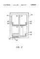
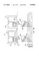
- FIG. 1is a cut-away perspective view illustrating a stack of segments.
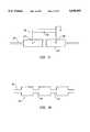
- FIG. 2is a diagram illustrating an address signal extending to four die on a segment through conductive fuses.
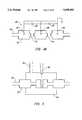
- FIG. 3is a diagram illustrating a conductive fuse of the present invention, and one preferred method of opening the conductive fuse using a circuit.
- FIGS. 4A and 4Bare diagrams illustrating a second preferred embodiment of the conductive fuse, and a method of opening the conductive fuse using a circuit of the present invention.
- FIG. 5is a diagram illustrating a third preferred embodiment of opening a conductive fuse using a laser.
- FIG. 6is a diagram illustrating a method of segment level programming according to the present invention.
- FIG. 7is a diagram illustrating a stack that is subsurface mounted in a circuit board.
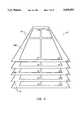
- FIG. 8is a perspective view illustrating a stack comprising five levels of segments.
- FIG. 9is a top view of a stack and a circuit board showing how the die on each segment are addressed by external circuits.
- FIGS. 10A and 10Bare top views of a stack and a circuit board showing how a defective die in the stack is logically replaced with a functional die in the stack.
- FIG. 1a cut-away perspective view is shown of a stack 10 of the present invention.
- the stack 10includes four segments, 12a, 12b, 12c, and 12d (hereinafter segments 12) where each of the segments 12 represent a different level in the stack 10.
- the segments 12each include four die 14 arranged in a two-by-two matrix, as shown by the positional overlay of the four die 14 on each level of the stack.
- each of the die 14 on the segments 12are interconnected using multiple layers of die interconnect circuitry.
- the die interconnect circuitry on each segment 12includes two layers of gold interconnects 34 and 40 which function to communicate power and electrical signals between die bond pads 20 as well as to selected segment bond pads 22.
- the die 14first are insulated with a polyimide layer 30 that covers the entire surface 24 of the segments 12 except for a first set of holes 32 in the polyimide layer 30 which expose the surface of the die bond pads 20.
- the first layer of gold interconnects 34is supported by the polyimide layer 30 and makes electrical connection to the die bond pads 20 through the first set of holes 32.
- the first layer of gold interconnects 34is insulated with a second polyimide layer 36, and a second set of holes 38 in the second polyimide layer 36 exposes selected portions of the first layer of gold interconnects 34.
- the second layer of gold interconnects 40is supported by the second polyimide layer 36 and makes electrical connection with the first layer of gold interconnects 34 through the second set of holes 38.
- a third polyimide layer 42insulates the second layer of gold interconnects 40, and cutouts 44 around the four edges of the segments 12 expose selected portions of the second layer of gold interconnects 40, forming the segment bond pads 22.
- electrically conductive epoxy traces 46are dispensed along the edges of the stack 10 in contact with the segment bond pads 22 on each of the segments 12.
- the electrically conductive epoxy traces 46also function to allow external electrical circuits to address the segments 12 after the segments are programmed, as explained below.
- FIG. 2a diagram showing conductive fuses 50 of the present invention located on a segment 12 that enable the segment 12 and the die 14 thereon to be programmed.
- Every electrical signal transmitted to the segment 12, including power and ground,must first enter the segment 12 through a segment bond pad 22.
- Address signal A0is shown, for instance, entering the segment 12 through segment bond pad 22, and then connecting to the four die 14 (D1, D2, D3 and D4).
- the A0 signalBefore connecting to the die bond pads 20, the A0 signal must first pass through a respective conductive fuse 50.
- the second layer of gold interconnects 40(FIG. 1) not only carry signals from the segment bond pads 22 to the die bond pads 20, but also form the conductive fuses 50.
- the segments 12are first tested for functionality.
- the defective die D3if one of the die 14 is found to be defective (e.g., die D3), the defective die D3 is not physically cut out and discarded as in prior art methods, but is rather electrically disconnected from the segment 12.
- defective die 14are disconnected by electrically opening the respective conductive fuse 50 on the second layer of gold interconnects 40 (hereinafter gold interconnect 40) of the defective die 14.
- FIG. 3is a diagram depicting one embodiment of the present invention for electrically opening a conductive fuse 50 using a circuit 60.
- the conductive fuse 50is formed from a generally rectangular portion of gold interconnect 40, although other shapes are also suitable.
- the circuit 60 used to open the conductive fuse 50includes a charged capacitor 62 which is located between two probes 64 and 66. Once the probes 64 and 66 contact the conductive fuse 50, the capacitor 62 applies a positive voltage to probe 64 and a negative voltage to probe 66. The resulting current created between the probes 64 and 66 is larger than the capacity of the conducting fuse 50 and causes the conducting fuse 50 to physically open.
- One disadvantage with the structure of the conductive fuse 50 shown in FIG. 3is that during the process of opening the conductive fuse 50, the current created by the capacitor 62 often times escapes across the gold interconnect 40 and damages the die circuitry.
- Another disadvantage with the structure of the conductive fuse 50is that not every attempt to open a conductive fuse 50 by the circuit 60 will succeed, because in some instances, the voltage generated by the circuit 60 is insufficient to overcome the capacitance of the conductive fuse 50. Thus, defective die may unintentionally remain electrically connected to a segment and result in a segment that may not function properly.
- FIG. 4Ais a diagram showing a second embodiment of the conductive fuse 50 of the present invention.
- the conductive fuse 50includes a dual fuse structure wherein fuse 72 is connected in series with fuse 74. Because fuses 72 and 74 are smaller in area than the surrounding areas of the conductive fuse 50, the fuses 72 and 74 also have less electrical resistance and require less voltage to be opened.
- FIG. 4Bis a diagram showing one method for opening the conductive fuse 50 of FIG. 4A, using a three probe circuit 80.
- the three probe circuit 80includes two outer probes 82 and 84 and one center probe 86.
- a first capacitor 88is located between the outer probe 82 and the center probe 86
- a second capacitor 90is located between the center probe 86 and the outer probe 84.
- the three probe circuit 80 and the dual fuse structure of the conductive fuse 50provide several advantages.
- One advantageis that the three probe structure of the circuit 80 prevents the current from escaping across the gold interconnect 40 and damaging nearby circuits because the current created by the capacitors 88 and 90 is trapped between the two outer probes 82 and 84.
- Another advantageis that the dual fuse structure of the conductive fuse 50 increases the likelihood that the conductive fuse 50 will be opened by the current produced by the three probe circuit 80.
- the current generated by the three probe circuit 80is sufficient to disconnect a defective die 14 by opening both fuse 72 and fuse 74. In some instances, however, the three probe circuit 80 may only open either fuse 72 or fuse 74.
- the two fuse structure of the conductive fuse 50increases the chances that the conductive fuse 50 will be opened to disconnect a die 14, thereby increasing the yield rate for segments 12 possessing the desired functionality.
- FIG. 5is a diagram of a third embodiment of opening a conductive fuse 50.
- defective die 14(FIG. 2) are disconnected using a laser 92 to vaporize and open the center portion of a conductive fuse 50. Since the energy from the laser 92 is sufficient to penetrate the gold interconnect 40, which forms the conductive fuse 50, the laser 92 is also capable of destroying the circuitry of the die 14 on a segment 12.
- the first layer of gold interconnects 34is patterned on the segment 12 underneath each conductive fuse 50 into a heat shield 94 to protect the die 14 from the laser 92.
- the width of the heat shield 94is sufficiently larger than the width of the conductive fuse 50 so that the laser 92 may be activated at a point inside the heat shield 94, but outside the conductive fuse 50.
- the energy of the laser 92is adjusted so it vaporizes the top layer of gold interconnects 40, but not the heat shield 94 underneath.
- the segments 12are programmed so that external decoding circuitry may access each segment 12 in the stack 10.
- programmingrefers to the process of routing control lines so that redundant functional die 14 replace the disconnected defective die 14. This is accomplished by connecting the control lines originally intended for the disconnected die 14 to the replacement die 14. Programming is necessary because once the segments 12 are stacked and become operative, a computer or the like may attempt to access a disconnected die 14 in the stack 10. Therefore, the segments 12 that have defective die 14 must be programmed so that when an attempt is made to access a defective die 14 in a stack 10, a functioning die 14 is accessed instead.
- segment level programmingwhich occurs during the fabrication of a stack 10 refers to the process in which each segment 12 in a stack is made unique with respect to one another.
- Circuit board level programmingwhich occurs once a stack 10 is connected to external circuits, refers to the process of logically replacing defective die 14 in the stack 10 with functioning die 14 in the stack 10, described further below.
- a segment 12 having four die 14(D1, D2, D3, and D4) is shown, on which segment level programming has been performed according to the present invention.
- each die on the segment 12is externally addressed through a conventional row address strobe (RAS) signal 98.
- RASrow address strobe
- the interface between the RAS signal 98 and a die 14comprises a set of segment control-bond-pads 100 and corresponding die control-bond-pads 102 equal to the number of levels in the stack.
- Each individual set of control-bond-pads 100 and 102is assigned to a different level in the stack.
- each segment 12 in a stack 10is made unique with respect to one another by leaving intact the conductive fuse 50 assigned to the level that the segment 12 occupies in the stack 10.
- the conductive fuses 50 assigned to other levels in the stack 10are opened. If, for example, the segment 12 in FIG. 6 occupies level two in a stack 10, then all the fuses 50 would be opened (using the methods described above), except the conductive fuse 50 assigned to level L2, as shown. Similarly, the segment 12 occupying level three (not shown) in the stack 10 would have all the conductive fuses 50 opened except the conductive fuse 50 assigned to level L3, and so on for each level in the stack 10.
- the RAS signal 98is subsequently activated, only the segment 12 whose conductive fuses 50 are intact for that level will receive the RAS signal 98.
- the segments 12are stacked, and the stack 10 is electrically connected to external circuits, typically located on a circuit board for example.
- the stack 10is subsurface mounted to a circuit board, rather than mounted on the surface of the circuit board, and electrical contact is made between the stack 10 and the circuits on the circuit board through the use of electrically conductive epoxy.
- a circuit board 150is shown with a stack 10 subsurface mounted therein.
- the stack 10is placed in a hole 154 cut into the circuit board 150 so that the top segment 12 of the stack 10 is coplaner with the surface of the printed circuit board 150, as shown.
- the stack 10is held in place by small drops of fast-curing positional epoxy 158 applied at various locations around the perimeter of the stack 10.
- the circuit board 150includes a plurality of metal traces 160 which represent control signals.
- the stack 10is positioned in the circuit board 150 so that the segment control-bond-pads 22 around the perimeter of the top segment 12 match the positions of the metal traces 160 on the circuit board 150.
- a dispense mechanism 132applies silver filled conductive epoxy between each segment control-bond-pad 22 and an opposing metal trace 160 on the circuit board 150 forming epoxy whiskers 162.
- the epoxy whiskers 162along with the epoxy traces 46 (FIG. 1), which are dispensed along the edges of the stack 10, interconnect the segments 12 in the stack 10 and provide an electrical connection between the circuit board 150 and the stack 10.
- the RAS signal 98originates from the circuit board 150 in the form of metal traces 160 and extends to each segment 12 in the stack 10 via the epoxy whiskers 162 and epoxy traces 64.
- segment level programming of the present inventionenables circuitry on the circuit board 150 to access any segment 12 in the stack 10.
- FIG. 8is a perspective view of a stack 10, which includes five levels of segments 12, labeled L1, L2, L3, L4, and L5, where each segment 12 includes four die 14 (D1, D2, D3, and D4).
- each segment 12includes four die 14 (D1, D2, D3, and D4).
- semiconductor devicessuch as die 14 to fail after a short period of operation.
- a defective die 180 (D1) within a segment 12 of the stack 10fails, the defective die 180 cannot be physically removed without damaging both the segment 12 and the stack 10. Die 14 failures are therefore remedied by logically replacing the defective die 180 with a functioning die 14 in the stack 10 through circuit board level programming.
- level L5is provided as a redundant level to supply replacement die 14.
- level L5only a replacement die 14 that is located in the same vertical column in the stack 10 as a defective die 180 is used to replace the defective die 180. Therefore, only the replacement die 182 on the redundant level L5 may be used to replace the defective die 180 on level L3 because both die 180 and 182 are in the same vertical column in the stack 10.
- the defective die 180is first electrically disconnected from the segment 12, as described above.
- the RAS signal 98 (FIG. 6) of the defective die 180is routed to the replacement die 182 in accordance with the present invention.
- FIG. 9is a top view of a segment 12 in a stack 10 and a circuit board 150, showing how segments 12 are addressed from the circuit board 150 to allow the logical replacement of die 14 in the stack 10.
- the segment 12which as an example is shown occupying level three (L3) in the stack 10, is addressed from the circuit board 150 through a set of RAS lines 200, and a set of metal switches 202.
- the set of RAS lines 200includes a separate RAS line for each level in a stack 10, plus a line indicating no signal, called OFF.
- a stack 10 having five levelsrequire six lines, one for each level in the stack and one for off, shown in FIG. 9 as RAS L1, RAS L2, RAS L3, RAS L4, RAS L5, and OFF.
- each die 14 in the stack 10is addressed through a separate RAS signal 98.
- a metal switch 202Connected between each RAS signal 98 and the RAS L1, RAS L2, RAS L3, RAS L4, RAS L5, and OFF lines, is a metal switch 202.
- RAS signal 98 and one metal switch 202is shown for die D1 in FIG. 9, it is to be understood that every die 14 on each level in the stack 10 is connected to a RAS signal 98 and a corresponding metal switch 202.
- the purpose of the metal switch 202is to provide a flexible method for routing one of the RAS lines 200 to a RAS signal 98.
- the metal switch 202is made of copper, although other conductive metals are also suitable.
- the metal switch 202is capable of routing any of the RAS lines 200 to a corresponding RAS signal 98 through the use of an epoxy whisker 162 which is applied between the metal switch 202 and the selected RAS line 200.
- every die 14 on a segment 12 in a stack 10is connected to the RAS line 200 assigned to the level the segment 12 occupies. As shown in FIG. 9, since the segment 12 occupies level L3 in the stack, each die 14 on the segment 12 is connected to the RAS L3 line by dispensing an epoxy whisker 162 between each metal switch 202 and the RAS L3 line. When a die 14 is found to be defective, then the defective 14 is logically replaced with a functioning die 14 by rerouting the RAS line 200 originally assigned to the defective die 14 to a redundant functioning die 14 using each of the die's respective metal switches 202.
- FIGS. 10A and 10Billustrate how the metal switches 202 are utilized during circuit board programming to logically replace a defective die 180 in a stack 10 with a functioning die 182.
- the stack 10 showncontains five levels (L1 through L5) where level L5 is redundant.
- Level L3 in the stack 10contains the defective die 180 which must be logically replaced with the replacement die 182 on level L5.
- FIG. 10Ashows how the die 14 on both levels L3 and L5 are addressed in the stack 10 before it is discovered that die 180 is defective.
- FIG. 10Bshows how the defective die 180 on level L3 and the replacement die 182 on level L5 are addressed after circuit board programming.
- the segment 12 on level L3is addressed as described with reference to FIG. 9.
- the die 180is originally connected to the RAS L3 line by an epoxy whisker 162A that is connected between the RAS L3 line and the metal switch 202A.
- the RAS signal 98Ais connected between the metal switch 202A and the defective die 180 through the conductive fuse 50A.
- level L5is not originally connected to a RAS line 200, since level L5 in the stack 10 is redundant and is not required to be addressed from the circuit board 150. Also, the die 14 on level L5 are assigned to level L5 in the stack during segment level programming by connecting the RAS signal 98B to the conductive fuse 50B assigned to level L5, and opening the remaining fuses.
- circuit board programmingis used to replace the defective die 180 in level L3 with the replacement die 182 in level L5.
- the first step in circuit board programmingis to electrically disconnect the defective die 180 from level L3.
- the defective die 180is first electrically disconnected from level L3 by moving the epoxy whisker 162A from the metal switch 202A and the RAS L3 line and placing the epoxy whisker 162A between the metal switch 202A and the OFF line.
- the defective die 180may be electrically disconnected from level L3 by opening the fuse 50A (see FIG. 10A) assigned to level L3.
- the RAS L3 lineis re-routed to the replacement die 182 in level L5 by dispensing an epoxy whisker 162B between the metal switch 202B and the RAS L3 line. Since the RAS L3 line is now routed to the replacement die 182 through the metal switch 202B and the RAS 98B signal, when an attempt is subsequently made to access the defective die 180 through the RAS L3 line, the replacement die 182 will be accessed instead.
- the remaining die 14 on level L5may be used to replace other defective die found on any level within the stack 10, as described above.
- a functioning electronic devicerequired a stack of four functioning segments.
- the stackis fabricated so that four redundant levels of segments may be added to the stack, providing a stack of eight segments. Creating a stack having equal numbers of redundant segments as required segments provides a functioning electronic device where only 50% of the die in the stack function properly.
- a method and apparatushas been disclosed for segment level programming and circuit board level programming a stack of segments.
- the programming methods of the present inventionenable external circuits to uniquely address segments within a stack.
- the programming methods and apparatus of the present inventionmay also be used to uniquely address individual chips, rather than segments.
Landscapes
- Engineering & Computer Science (AREA)
- Microelectronics & Electronic Packaging (AREA)
- Power Engineering (AREA)
- Computer Hardware Design (AREA)
- Physics & Mathematics (AREA)
- Condensed Matter Physics & Semiconductors (AREA)
- General Physics & Mathematics (AREA)
- Manufacturing & Machinery (AREA)
- Chemical & Material Sciences (AREA)
- Materials Engineering (AREA)
- Design And Manufacture Of Integrated Circuits (AREA)
Abstract
Description
Claims (6)
Priority Applications (5)
| Application Number | Priority Date | Filing Date | Title |
|---|---|---|---|
| US08/376,149US5698895A (en) | 1994-06-23 | 1995-01-20 | Silicon segment programming method and apparatus |
| PCT/US1995/017020WO1996022622A1 (en) | 1995-01-20 | 1995-12-28 | Silicon segment programming method and apparatus |
| AU47441/96AAU4744196A (en) | 1995-01-20 | 1995-12-28 | Silicon segment programming method and apparatus |
| US08/845,655US5936302A (en) | 1994-06-23 | 1997-04-25 | Speaker diaphragm |
| US08/845,654US5994170A (en) | 1994-06-23 | 1997-04-25 | Silicon segment programming method |
Applications Claiming Priority (2)
| Application Number | Priority Date | Filing Date | Title |
|---|---|---|---|
| US08/265,081US5675180A (en) | 1994-06-23 | 1994-06-23 | Vertical interconnect process for silicon segments |
| US08/376,149US5698895A (en) | 1994-06-23 | 1995-01-20 | Silicon segment programming method and apparatus |
Related Parent Applications (1)
| Application Number | Title | Priority Date | Filing Date |
|---|---|---|---|
| US08/265,081Continuation-In-PartUS5675180A (en) | 1994-06-23 | 1994-06-23 | Vertical interconnect process for silicon segments |
Related Child Applications (2)
| Application Number | Title | Priority Date | Filing Date |
|---|---|---|---|
| US08/845,654DivisionUS5994170A (en) | 1994-06-23 | 1997-04-25 | Silicon segment programming method |
| US08/845,655ContinuationUS5936302A (en) | 1994-06-23 | 1997-04-25 | Speaker diaphragm |
Publications (1)
| Publication Number | Publication Date |
|---|---|
| US5698895Atrue US5698895A (en) | 1997-12-16 |
Family
ID=23483902
Family Applications (3)
| Application Number | Title | Priority Date | Filing Date |
|---|---|---|---|
| US08/376,149Expired - LifetimeUS5698895A (en) | 1994-06-23 | 1995-01-20 | Silicon segment programming method and apparatus |
| US08/845,654Expired - LifetimeUS5994170A (en) | 1994-06-23 | 1997-04-25 | Silicon segment programming method |
| US08/845,655Expired - LifetimeUS5936302A (en) | 1994-06-23 | 1997-04-25 | Speaker diaphragm |
Family Applications After (2)
| Application Number | Title | Priority Date | Filing Date |
|---|---|---|---|
| US08/845,654Expired - LifetimeUS5994170A (en) | 1994-06-23 | 1997-04-25 | Silicon segment programming method |
| US08/845,655Expired - LifetimeUS5936302A (en) | 1994-06-23 | 1997-04-25 | Speaker diaphragm |
Country Status (3)
| Country | Link |
|---|---|
| US (3) | US5698895A (en) |
| AU (1) | AU4744196A (en) |
| WO (1) | WO1996022622A1 (en) |
Cited By (36)
| Publication number | Priority date | Publication date | Assignee | Title |
|---|---|---|---|---|
| US5781791A (en)* | 1996-04-16 | 1998-07-14 | The United States Of America As Represented By The Secretary Of The Army | Digital microelectronic circuit package using buffer dies and programmable device or memory dies |
| WO2000007240A1 (en)* | 1998-07-27 | 2000-02-10 | Reveo, Inc. | Three-dimensional packaging technology for multi-layered integrated circuits |
| US6189109B1 (en) | 1997-05-13 | 2001-02-13 | Micron Electronics, Inc. | Method of remote access and control of environmental conditions |
| US6355976B1 (en) | 1992-05-14 | 2002-03-12 | Reveo, Inc | Three-dimensional packaging technology for multi-layered integrated circuits |
| US6486528B1 (en)* | 1994-06-23 | 2002-11-26 | Vertical Circuits, Inc. | Silicon segment programming apparatus and three terminal fuse configuration |
| US6621155B1 (en) | 1999-12-23 | 2003-09-16 | Rambus Inc. | Integrated circuit device having stacked dies and impedance balanced transmission lines |
| US20030193786A1 (en)* | 2002-04-15 | 2003-10-16 | Ralf Greiner | Compact circuit carrier package |
| US6664632B2 (en) | 1999-01-13 | 2003-12-16 | Micron Technologies, Inc. | Utilization of die active surfaces for laterally extending die internal and external connections |
| US20040190273A1 (en)* | 2003-03-31 | 2004-09-30 | Siliconware Precision Industries | Chip carrier and method for testing electrical performance of passive component |
| US20050258530A1 (en)* | 2004-04-13 | 2005-11-24 | Al Vindasius | Micropede stacked die component assembly |
| US20050258504A1 (en)* | 2004-05-19 | 2005-11-24 | United Microelectronics Corp. | Fuse structure for a semiconductor device |
| US7215018B2 (en) | 2004-04-13 | 2007-05-08 | Vertical Circuits, Inc. | Stacked die BGA or LGA component assembly |
| US20080071934A1 (en)* | 2006-09-15 | 2008-03-20 | Microsoft Corporation | Smart Interconnect For Modular Multi-Component Embedded Devices |
| US20080315407A1 (en)* | 2007-06-20 | 2008-12-25 | Vertical Circuits, Inc. | Three-dimensional circuitry formed on integrated circuit device using two-dimensional fabrication |
| WO2008154582A3 (en)* | 2007-06-11 | 2009-02-19 | Vertical Circuits Inc | Semiconductor die coating and interconnection fixture and method |
| WO2008154580A3 (en)* | 2007-06-11 | 2009-02-19 | Vertical Circuits Inc | Method for optimized integrated circuit chip interconnection |
| US20090065916A1 (en)* | 2007-09-10 | 2009-03-12 | Vertical Circuits, Inc. | Semiconductor die mount by conformal die coating |
| WO2009045763A1 (en)* | 2007-10-02 | 2009-04-09 | Micron Technology, Inc. | Systems, methods and devices for arbitrating die stack position in a multi-die stack device |
| US20090230528A1 (en)* | 2008-03-12 | 2009-09-17 | Vertical Circuits, Inc. | Support Mounted Electrically Interconnected Die Assembly |
| US7705432B2 (en) | 2004-04-13 | 2010-04-27 | Vertical Circuits, Inc. | Three dimensional six surface conformal die coating |
| US20100327461A1 (en)* | 2009-06-26 | 2010-12-30 | Vertical Circuits, Inc. | Electrical interconnect for die stacked in zig-zag configuration |
| US20110037159A1 (en)* | 2007-06-11 | 2011-02-17 | Vertical Circuits, Inc. | Electrically Interconnected Stacked Die Assemblies |
| US20110101505A1 (en)* | 2008-06-19 | 2011-05-05 | Vertical Circuits, Inc. | Semiconductor Die Separation Method |
| US20120032318A1 (en)* | 2010-08-09 | 2012-02-09 | Sae Magnetics (H.K.) Ltd. | Layered chip package and method of manufacturing same |
| US20120112352A1 (en)* | 2010-11-10 | 2012-05-10 | Taiwan Semiconductor Manufacturing Company, Ltd. | Integrated circuit system with distributed power supply |
| US8912661B2 (en) | 2009-11-04 | 2014-12-16 | Invensas Corporation | Stacked die assembly having reduced stress electrical interconnects |
| US9147583B2 (en) | 2009-10-27 | 2015-09-29 | Invensas Corporation | Selective die electrical insulation by additive process |
| US9153517B2 (en) | 2008-05-20 | 2015-10-06 | Invensas Corporation | Electrical connector between die pad and z-interconnect for stacked die assemblies |
| US9490195B1 (en) | 2015-07-17 | 2016-11-08 | Invensas Corporation | Wafer-level flipped die stacks with leadframes or metal foil interconnects |
| US9508691B1 (en) | 2015-12-16 | 2016-11-29 | Invensas Corporation | Flipped die stacks with multiple rows of leadframe interconnects |
| US9595511B1 (en) | 2016-05-12 | 2017-03-14 | Invensas Corporation | Microelectronic packages and assemblies with improved flyby signaling operation |
| US9728524B1 (en) | 2016-06-30 | 2017-08-08 | Invensas Corporation | Enhanced density assembly having microelectronic packages mounted at substantial angle to board |
| US9825002B2 (en) | 2015-07-17 | 2017-11-21 | Invensas Corporation | Flipped die stack |
| US9871019B2 (en) | 2015-07-17 | 2018-01-16 | Invensas Corporation | Flipped die stack assemblies with leadframe interconnects |
| US10566310B2 (en) | 2016-04-11 | 2020-02-18 | Invensas Corporation | Microelectronic packages having stacked die and wire bond interconnects |
| US10636767B2 (en)* | 2016-02-29 | 2020-04-28 | Invensas Corporation | Correction die for wafer/die stack |
Families Citing this family (14)
| Publication number | Priority date | Publication date | Assignee | Title |
|---|---|---|---|---|
| US6337507B1 (en) | 1995-09-29 | 2002-01-08 | Intel Corporation | Silicide agglomeration fuse device with notches to enhance programmability |
| US5895942A (en)* | 1996-06-18 | 1999-04-20 | Kabushiki Kaisha Toshiba | Fuse selectable modules |
| DE19743264C2 (en)* | 1997-09-30 | 2002-01-17 | Infineon Technologies Ag | Method for producing an emulation circuit arrangement and emulation circuit arrangement with two integrated circuits |
| US6376784B1 (en)* | 1997-12-27 | 2002-04-23 | Ishida Co., Ltd. | Vibrating transport apparatus and method of detecting vibration characteristic |
| US6414542B2 (en)* | 1999-03-17 | 2002-07-02 | Koninklijke Philips Electronics N.V. | Integrated circuit with relative sense inversion of signals along adjacent parallel signal paths |
| WO2000067319A1 (en)* | 1999-05-03 | 2000-11-09 | Infineon Technologies Ag | Security method and device for a chip stack with a multidimensional structure |
| DE10044148A1 (en)* | 2000-09-06 | 2002-03-21 | Infineon Technologies Ag | Electronic component with stacked components and process for its manufacture |
| US6680578B2 (en)* | 2001-09-19 | 2004-01-20 | Osram Opto Semiconductors, Gmbh | Organic light emitting diode light source |
| US7183623B2 (en)* | 2001-10-02 | 2007-02-27 | Agere Systems Inc. | Trimmed integrated circuits with fuse circuits |
| JP3828473B2 (en)* | 2002-09-30 | 2006-10-04 | 株式会社東芝 | Multilayer semiconductor device and manufacturing method thereof |
| US7208776B2 (en)* | 2004-01-30 | 2007-04-24 | Broadcom Corporation | Fuse corner pad for an integrated circuit |
| US8319326B2 (en)* | 2010-09-30 | 2012-11-27 | Apple Inc. | Stacked die with vertically-aligned conductors and methods for making the same |
| GB2506154B (en)* | 2012-09-21 | 2015-03-18 | Control Tech Ltd | DC Link Capacitor Bank |
| US9351060B2 (en) | 2014-02-14 | 2016-05-24 | Sonic Blocks, Inc. | Modular quick-connect A/V system and methods thereof |
Citations (82)
| Publication number | Priority date | Publication date | Assignee | Title |
|---|---|---|---|---|
| US3679941A (en)* | 1969-09-22 | 1972-07-25 | Gen Electric | Composite integrated circuits including semiconductor chips mounted on a common substrate with connections made through a dielectric encapsulator |
| US3691628A (en)* | 1969-10-31 | 1972-09-19 | Gen Electric | Method of fabricating composite integrated circuits |
| US3702025A (en)* | 1969-05-12 | 1972-11-07 | Honeywell Inc | Discretionary interconnection process |
| US3769702A (en)* | 1971-02-01 | 1973-11-06 | Bunker Ramo | 3d-coaxial memory construction and method of making |
| US3813773A (en)* | 1972-09-05 | 1974-06-04 | Bunker Ramo | Method employing precision stamping for fabricating the wafers of a multiwafer electrical circuit structure |
| US3999105A (en)* | 1974-04-19 | 1976-12-21 | International Business Machines Corporation | Liquid encapsulated integrated circuit package |
| EP0010657A1 (en)* | 1978-10-18 | 1980-05-14 | General Electric Company | Selective etching of polymeric materials embodying silicones via reactor plasmas |
| US4300153A (en)* | 1977-09-22 | 1981-11-10 | Sharp Kabushiki Kaisha | Flat shaped semiconductor encapsulation |
| WO1983000131A1 (en)* | 1981-06-30 | 1983-01-20 | Juhl, Britta | Packaging article for a stack of gaskets, in particular those made of plastic deformable material |
| US4426773A (en)* | 1981-05-15 | 1984-01-24 | General Electric Ceramics, Inc. | Array of electronic packaging substrates |
| US4525921A (en)* | 1981-07-13 | 1985-07-02 | Irvine Sensors Corporation | High-density electronic processing package-structure and fabrication |
| EP0175870A2 (en)* | 1981-01-16 | 1986-04-02 | Mosaic Systems, Inc. | Wafer scale integrated circuit device |
| EP0178227A2 (en)* | 1984-10-05 | 1986-04-16 | Fujitsu Limited | Integrated circuit semiconductor device formed on a wafer |
| US4612083A (en)* | 1984-07-20 | 1986-09-16 | Nec Corporation | Process of fabricating three-dimensional semiconductor device |
| US4613891A (en)* | 1984-02-17 | 1986-09-23 | At&T Bell Laboratories | Packaging microminiature devices |
| US4646128A (en)* | 1980-09-16 | 1987-02-24 | Irvine Sensors Corporation | High-density electronic processing package--structure and fabrication |
| US4659931A (en)* | 1985-05-08 | 1987-04-21 | Grumman Aerospace Corporation | High density multi-layered integrated circuit package |
| US4672737A (en)* | 1984-01-23 | 1987-06-16 | Irvine Sensors Corporation | Detector array module fabrication process |
| US4677528A (en)* | 1984-05-31 | 1987-06-30 | Motorola, Inc. | Flexible printed circuit board having integrated circuit die or the like affixed thereto |
| US4703170A (en)* | 1985-04-12 | 1987-10-27 | Grumman Aerospace Corporation | Infrared focal plane module |
| US4706166A (en)* | 1986-04-25 | 1987-11-10 | Irvine Sensors Corporation | High-density electronic modules--process and product |
| US4761681A (en)* | 1982-09-08 | 1988-08-02 | Texas Instruments Incorporated | Method for fabricating a semiconductor contact and interconnect structure using orientation dependent etching and thermomigration |
| US4764846A (en)* | 1987-01-05 | 1988-08-16 | Irvine Sensors Corporation | High density electronic package comprising stacked sub-modules |
| US4783695A (en)* | 1986-09-26 | 1988-11-08 | General Electric Company | Multichip integrated circuit packaging configuration and method |
| US4801992A (en)* | 1986-12-01 | 1989-01-31 | Motorola Inc. | Three dimensional interconnected integrated circuit |
| US4803595A (en)* | 1986-11-17 | 1989-02-07 | International Business Machines Corporation | Interposer chip technique for making engineering changes between interconnected semiconductor chips |
| US4807021A (en)* | 1986-03-10 | 1989-02-21 | Kabushiki Kaisha Toshiba | Semiconductor device having stacking structure |
| US4827327A (en)* | 1985-04-13 | 1989-05-02 | Fujitsu Limited | Integrated circuit device having stacked conductive layers connecting circuit elements therethrough |
| US4835593A (en)* | 1986-05-07 | 1989-05-30 | International Business Machines Corporation | Multilayer thin film metallurgy for pin brazing |
| US4862249A (en)* | 1987-04-17 | 1989-08-29 | Xoc Devices, Inc. | Packaging system for stacking integrated circuits |
| US4894706A (en)* | 1985-02-14 | 1990-01-16 | Nippon Telegraph And Telephone Corporation | Three-dimensional packaging of semiconductor device chips |
| US4897708A (en)* | 1986-07-17 | 1990-01-30 | Laser Dynamics, Inc. | Semiconductor wafer array |
| US4901136A (en)* | 1987-07-14 | 1990-02-13 | General Electric Company | Multi-chip interconnection package |
| US4907128A (en)* | 1988-12-15 | 1990-03-06 | Grumman Aerospace Corporation | Chip to multilevel circuit board bonding |
| US4939568A (en)* | 1986-03-20 | 1990-07-03 | Fujitsu Limited | Three-dimensional integrated circuit and manufacturing method thereof |
| US4941033A (en)* | 1988-12-27 | 1990-07-10 | Mitsubishi Denki Kabushiki Kaisha | Semiconductor integrated circuit device |
| US4954875A (en)* | 1986-07-17 | 1990-09-04 | Laser Dynamics, Inc. | Semiconductor wafer array with electrically conductive compliant material |
| US4956695A (en)* | 1989-05-12 | 1990-09-11 | Rockwell International Corporation | Three-dimensional packaging of focal plane assemblies using ceramic spacers |
| US4956694A (en)* | 1988-11-04 | 1990-09-11 | Dense-Pac Microsystems, Inc. | Integrated circuit chip stacking |
| US4956746A (en)* | 1989-03-29 | 1990-09-11 | Hughes Aircraft Company | Stacked wafer electronic package |
| US4959749A (en)* | 1989-08-16 | 1990-09-25 | Unisys Corporation | Layered electronic assembly having compensation for chips of different thickness and different I/O lead offsets |
| US4983533A (en)* | 1987-10-28 | 1991-01-08 | Irvine Sensors Corporation | High-density electronic modules - process and product |
| US4989063A (en)* | 1988-12-09 | 1991-01-29 | The United States Of America As Represented By The Secretary Of The Air Force | Hybrid wafer scale microcircuit integration |
| US4996583A (en)* | 1989-02-15 | 1991-02-26 | Matsushita Electric Industrial Co., Ltd. | Stack type semiconductor package |
| US5006923A (en)* | 1989-09-14 | 1991-04-09 | Litton Systems, Inc. | Stackable multilayer substrate for mounting integrated circuits |
| WO1991005478A1 (en)* | 1989-10-11 | 1991-05-02 | Cabinplant Development A/S | A method of operating shrimp processing apparatuses and an apparatus for use in carrying out the method |
| US5013687A (en)* | 1989-07-27 | 1991-05-07 | Grumman Aerospace Corporation | Framed chip hybrid stacked layer assembly |
| US5019943A (en)* | 1990-02-14 | 1991-05-28 | Unisys Corporation | High density chip stack having a zigzag-shaped face which accommodates connections between chips |
| US5025306A (en)* | 1988-08-09 | 1991-06-18 | Texas Instruments Incorporated | Assembly of semiconductor chips |
| US5028986A (en)* | 1987-12-28 | 1991-07-02 | Hitachi, Ltd. | Semiconductor device and semiconductor module with a plurality of stacked semiconductor devices |
| US5032896A (en)* | 1989-08-31 | 1991-07-16 | Hughes Aircraft Company | 3-D integrated circuit assembly employing discrete chips |
| US5055425A (en)* | 1989-06-01 | 1991-10-08 | Hewlett-Packard Company | Stacked solid via formation in integrated circuit systems |
| US5093708A (en)* | 1990-08-20 | 1992-03-03 | Grumman Aerospace Corporation | Multilayer integrated circuit module |
| US5104820A (en)* | 1989-07-07 | 1992-04-14 | Irvine Sensors Corporation | Method of fabricating electronic circuitry unit containing stacked IC layers having lead rerouting |
| US5111278A (en)* | 1991-03-27 | 1992-05-05 | Eichelberger Charles W | Three-dimensional multichip module systems |
| US5117282A (en)* | 1990-10-29 | 1992-05-26 | Harris Corporation | Stacked configuration for integrated circuit devices |
| US5128831A (en)* | 1991-10-31 | 1992-07-07 | Micron Technology, Inc. | High-density electronic package comprising stacked sub-modules which are electrically interconnected by solder-filled vias |
| US5135556A (en)* | 1991-04-08 | 1992-08-04 | Grumman Aerospace Corporation | Method for making fused high density multi-layer integrated circuit module |
| US5138437A (en)* | 1987-07-27 | 1992-08-11 | Mitsubishi Denki Kabushiki Kaisha | Semiconductor integrated circuit device in which integrated circuit units having different functions are stacked in three dimensional manner |
| US5138438A (en)* | 1987-06-24 | 1992-08-11 | Akita Electronics Co. Ltd. | Lead connections means for stacked tab packaged IC chips |
| US5172303A (en)* | 1990-11-23 | 1992-12-15 | Motorola, Inc. | Electronic component assembly |
| US5191404A (en)* | 1989-12-20 | 1993-03-02 | Digital Equipment Corporation | High density memory array packaging |
| US5191405A (en)* | 1988-12-23 | 1993-03-02 | Matsushita Electric Industrial Co., Ltd. | Three-dimensional stacked lsi |
| US5198888A (en)* | 1987-12-28 | 1993-03-30 | Hitachi, Ltd. | Semiconductor stacked device |
| WO1993006315A1 (en)* | 1991-09-27 | 1993-04-01 | Kabushiki Kaisha Komatsu Seisakusho | Fine operation mode change-over device for hydraulic excavator |
| US5200300A (en)* | 1989-06-01 | 1993-04-06 | Hewlett-Packard Company | Methods for forming high density multi-chip carriers |
| US5202754A (en)* | 1991-09-13 | 1993-04-13 | International Business Machines Corporation | Three-dimensional multichip packages and methods of fabrication |
| US5222014A (en)* | 1992-03-02 | 1993-06-22 | Motorola, Inc. | Three-dimensional multi-chip pad array carrier |
| US5221642A (en)* | 1991-08-15 | 1993-06-22 | Staktek Corporation | Lead-on-chip integrated circuit fabrication method |
| US5229647A (en)* | 1991-03-27 | 1993-07-20 | Micron Technology, Inc. | High density data storage using stacked wafers |
| US5231304A (en)* | 1989-07-27 | 1993-07-27 | Grumman Aerospace Corporation | Framed chip hybrid stacked layer assembly |
| EP0558855A2 (en)* | 1992-03-02 | 1993-09-08 | AT&T Corp. | Circuit board stack with novel cross-over cells |
| US5247423A (en)* | 1992-05-26 | 1993-09-21 | Motorola, Inc. | Stacking three dimensional leadless multi-chip module and method for making the same |
| US5259110A (en)* | 1992-04-03 | 1993-11-09 | International Business Machines Corporation | Method for forming a multilayer microelectronic wiring module |
| WO1993023982A1 (en)* | 1992-05-11 | 1993-11-25 | Nchip, Inc. | Stacked devices for multichip modules |
| US5270571A (en)* | 1991-10-30 | 1993-12-14 | Amdahl Corporation | Three-dimensional package for semiconductor devices |
| US5270261A (en)* | 1991-09-13 | 1993-12-14 | International Business Machines Corporation | Three dimensional multichip package methods of fabrication |
| US5283107A (en)* | 1991-05-03 | 1994-02-01 | International Business Machines Corporation | Modular multilayer interwiring structure |
| US5311401A (en)* | 1991-07-09 | 1994-05-10 | Hughes Aircraft Company | Stacked chip assembly and manufacturing method therefor |
| US5330359A (en)* | 1993-03-26 | 1994-07-19 | The Whitaker Corporation | Socket for stacking integrated circuit chips |
| US5438166A (en)* | 1987-09-29 | 1995-08-01 | Microelectronics And Computer Technology Corporation | Customizable circuitry |
| US5444366A (en)* | 1991-01-11 | 1995-08-22 | Texas Instruments Incorporated | Wafer burn-in and test system |
Family Cites Families (22)
| Publication number | Priority date | Publication date | Assignee | Title |
|---|---|---|---|---|
| US28481A (en)* | 1860-05-29 | Mosaic veneer | ||
| US3983619A (en)* | 1968-01-26 | 1976-10-05 | Hitachi, Ltd. | Large scale integrated circuit array of unit cells and method of manufacturing same |
| US3646666A (en)* | 1970-01-02 | 1972-03-07 | Rca Corp | Fabrication of semiconductor devices |
| US3778886A (en)* | 1972-01-20 | 1973-12-18 | Signetics Corp | Semiconductor structure with fusible link and method |
| USRE28481E (en) | 1972-01-20 | 1975-07-15 | Semiconductor structure with fusible link and method | |
| US3803562A (en)* | 1972-11-21 | 1974-04-09 | Honeywell Inf Systems | Semiconductor mass memory |
| US4387503A (en)* | 1981-08-13 | 1983-06-14 | Mostek Corporation | Method for programming circuit elements in integrated circuits |
| US4598462A (en)* | 1983-04-07 | 1986-07-08 | Rca Corporation | Method for making semiconductor device with integral fuse |
| US5223735A (en)* | 1988-09-30 | 1993-06-29 | Mitsubishi Denki Kabushiki Kaisha | Semiconductor integrated circuit device in which circuit functions can be remedied or changed and the method for producing the same |
| FR2638894A1 (en) | 1988-11-04 | 1990-05-11 | Thomson Csf | Device and method for connecting and fixing components |
| US5075253A (en)* | 1989-04-12 | 1991-12-24 | Advanced Micro Devices, Inc. | Method of coplanar integration of semiconductor IC devices |
| EP0509065A1 (en)* | 1990-08-01 | 1992-10-21 | Staktek Corporation | Ultra high density integrated circuit packages, method and apparatus |
| US5475920A (en)* | 1990-08-01 | 1995-12-19 | Burns; Carmen D. | Method of assembling ultra high density integrated circuit packages |
| US5446620A (en)* | 1990-08-01 | 1995-08-29 | Staktek Corporation | Ultra high density integrated circuit packages |
| US5499160A (en)* | 1990-08-01 | 1996-03-12 | Staktek Corporation | High density integrated circuit module with snap-on rail assemblies |
| US5377077A (en)* | 1990-08-01 | 1994-12-27 | Staktek Corporation | Ultra high density integrated circuit packages method and apparatus |
| JP2909328B2 (en)* | 1992-11-02 | 1999-06-23 | 株式会社東芝 | Field programmable gate array |
| US5455740A (en)* | 1994-03-07 | 1995-10-03 | Staktek Corporation | Bus communication system for stacked high density integrated circuit packages |
| US5502333A (en)* | 1994-03-30 | 1996-03-26 | International Business Machines Corporation | Semiconductor stack structures and fabrication/sparing methods utilizing programmable spare circuit |
| TW278229B (en)* | 1994-12-29 | 1996-06-11 | Siemens Ag | Fuse structure for an integrated circuit device and method for manufacturing a fuse structure |
| FR2741475B1 (en)* | 1995-11-17 | 2000-05-12 | Commissariat Energie Atomique | METHOD OF MANUFACTURING A MICRO-ELECTRONICS DEVICE INCLUDING A PLURALITY OF INTERCONNECTED ELEMENTS ON A SUBSTRATE |
| US5844296A (en)* | 1996-09-20 | 1998-12-01 | Mosel Vitelic Corporation | Space saving laser programmable fuse layout |
- 1995
- 1995-01-20USUS08/376,149patent/US5698895A/ennot_activeExpired - Lifetime
- 1995-12-28AUAU47441/96Apatent/AU4744196A/ennot_activeAbandoned
- 1995-12-28WOPCT/US1995/017020patent/WO1996022622A1/enactiveApplication Filing
- 1997
- 1997-04-25USUS08/845,654patent/US5994170A/ennot_activeExpired - Lifetime
- 1997-04-25USUS08/845,655patent/US5936302A/ennot_activeExpired - Lifetime
Patent Citations (83)
| Publication number | Priority date | Publication date | Assignee | Title |
|---|---|---|---|---|
| US3702025A (en)* | 1969-05-12 | 1972-11-07 | Honeywell Inc | Discretionary interconnection process |
| US3679941A (en)* | 1969-09-22 | 1972-07-25 | Gen Electric | Composite integrated circuits including semiconductor chips mounted on a common substrate with connections made through a dielectric encapsulator |
| US3691628A (en)* | 1969-10-31 | 1972-09-19 | Gen Electric | Method of fabricating composite integrated circuits |
| US3769702A (en)* | 1971-02-01 | 1973-11-06 | Bunker Ramo | 3d-coaxial memory construction and method of making |
| US3813773A (en)* | 1972-09-05 | 1974-06-04 | Bunker Ramo | Method employing precision stamping for fabricating the wafers of a multiwafer electrical circuit structure |
| US3999105A (en)* | 1974-04-19 | 1976-12-21 | International Business Machines Corporation | Liquid encapsulated integrated circuit package |
| US4300153A (en)* | 1977-09-22 | 1981-11-10 | Sharp Kabushiki Kaisha | Flat shaped semiconductor encapsulation |
| EP0010657A1 (en)* | 1978-10-18 | 1980-05-14 | General Electric Company | Selective etching of polymeric materials embodying silicones via reactor plasmas |
| US4646128A (en)* | 1980-09-16 | 1987-02-24 | Irvine Sensors Corporation | High-density electronic processing package--structure and fabrication |
| EP0175870A2 (en)* | 1981-01-16 | 1986-04-02 | Mosaic Systems, Inc. | Wafer scale integrated circuit device |
| US4426773A (en)* | 1981-05-15 | 1984-01-24 | General Electric Ceramics, Inc. | Array of electronic packaging substrates |
| WO1983000131A1 (en)* | 1981-06-30 | 1983-01-20 | Juhl, Britta | Packaging article for a stack of gaskets, in particular those made of plastic deformable material |
| US4525921A (en)* | 1981-07-13 | 1985-07-02 | Irvine Sensors Corporation | High-density electronic processing package-structure and fabrication |
| US4761681A (en)* | 1982-09-08 | 1988-08-02 | Texas Instruments Incorporated | Method for fabricating a semiconductor contact and interconnect structure using orientation dependent etching and thermomigration |
| US4672737A (en)* | 1984-01-23 | 1987-06-16 | Irvine Sensors Corporation | Detector array module fabrication process |
| US4613891A (en)* | 1984-02-17 | 1986-09-23 | At&T Bell Laboratories | Packaging microminiature devices |
| US4677528A (en)* | 1984-05-31 | 1987-06-30 | Motorola, Inc. | Flexible printed circuit board having integrated circuit die or the like affixed thereto |
| US4612083A (en)* | 1984-07-20 | 1986-09-16 | Nec Corporation | Process of fabricating three-dimensional semiconductor device |
| EP0178227A2 (en)* | 1984-10-05 | 1986-04-16 | Fujitsu Limited | Integrated circuit semiconductor device formed on a wafer |
| US4894706A (en)* | 1985-02-14 | 1990-01-16 | Nippon Telegraph And Telephone Corporation | Three-dimensional packaging of semiconductor device chips |
| US4703170A (en)* | 1985-04-12 | 1987-10-27 | Grumman Aerospace Corporation | Infrared focal plane module |
| US4827327A (en)* | 1985-04-13 | 1989-05-02 | Fujitsu Limited | Integrated circuit device having stacked conductive layers connecting circuit elements therethrough |
| US4659931A (en)* | 1985-05-08 | 1987-04-21 | Grumman Aerospace Corporation | High density multi-layered integrated circuit package |
| US4807021A (en)* | 1986-03-10 | 1989-02-21 | Kabushiki Kaisha Toshiba | Semiconductor device having stacking structure |
| US4939568A (en)* | 1986-03-20 | 1990-07-03 | Fujitsu Limited | Three-dimensional integrated circuit and manufacturing method thereof |
| US4706166A (en)* | 1986-04-25 | 1987-11-10 | Irvine Sensors Corporation | High-density electronic modules--process and product |
| US4835593A (en)* | 1986-05-07 | 1989-05-30 | International Business Machines Corporation | Multilayer thin film metallurgy for pin brazing |
| US4954875A (en)* | 1986-07-17 | 1990-09-04 | Laser Dynamics, Inc. | Semiconductor wafer array with electrically conductive compliant material |
| US4897708A (en)* | 1986-07-17 | 1990-01-30 | Laser Dynamics, Inc. | Semiconductor wafer array |
| US4783695A (en)* | 1986-09-26 | 1988-11-08 | General Electric Company | Multichip integrated circuit packaging configuration and method |
| US4803595A (en)* | 1986-11-17 | 1989-02-07 | International Business Machines Corporation | Interposer chip technique for making engineering changes between interconnected semiconductor chips |
| US4801992A (en)* | 1986-12-01 | 1989-01-31 | Motorola Inc. | Three dimensional interconnected integrated circuit |
| US4764846A (en)* | 1987-01-05 | 1988-08-16 | Irvine Sensors Corporation | High density electronic package comprising stacked sub-modules |
| US4862249A (en)* | 1987-04-17 | 1989-08-29 | Xoc Devices, Inc. | Packaging system for stacking integrated circuits |
| US5138438A (en)* | 1987-06-24 | 1992-08-11 | Akita Electronics Co. Ltd. | Lead connections means for stacked tab packaged IC chips |
| US4901136A (en)* | 1987-07-14 | 1990-02-13 | General Electric Company | Multi-chip interconnection package |
| US5138437A (en)* | 1987-07-27 | 1992-08-11 | Mitsubishi Denki Kabushiki Kaisha | Semiconductor integrated circuit device in which integrated circuit units having different functions are stacked in three dimensional manner |
| US5438166A (en)* | 1987-09-29 | 1995-08-01 | Microelectronics And Computer Technology Corporation | Customizable circuitry |
| US4983533A (en)* | 1987-10-28 | 1991-01-08 | Irvine Sensors Corporation | High-density electronic modules - process and product |
| US5198888A (en)* | 1987-12-28 | 1993-03-30 | Hitachi, Ltd. | Semiconductor stacked device |
| US5028986A (en)* | 1987-12-28 | 1991-07-02 | Hitachi, Ltd. | Semiconductor device and semiconductor module with a plurality of stacked semiconductor devices |
| US5025306A (en)* | 1988-08-09 | 1991-06-18 | Texas Instruments Incorporated | Assembly of semiconductor chips |
| US4956694A (en)* | 1988-11-04 | 1990-09-11 | Dense-Pac Microsystems, Inc. | Integrated circuit chip stacking |
| US4989063A (en)* | 1988-12-09 | 1991-01-29 | The United States Of America As Represented By The Secretary Of The Air Force | Hybrid wafer scale microcircuit integration |
| US4907128A (en)* | 1988-12-15 | 1990-03-06 | Grumman Aerospace Corporation | Chip to multilevel circuit board bonding |
| US5191405A (en)* | 1988-12-23 | 1993-03-02 | Matsushita Electric Industrial Co., Ltd. | Three-dimensional stacked lsi |
| US4941033A (en)* | 1988-12-27 | 1990-07-10 | Mitsubishi Denki Kabushiki Kaisha | Semiconductor integrated circuit device |
| US4996583A (en)* | 1989-02-15 | 1991-02-26 | Matsushita Electric Industrial Co., Ltd. | Stack type semiconductor package |
| US4956746A (en)* | 1989-03-29 | 1990-09-11 | Hughes Aircraft Company | Stacked wafer electronic package |
| US4956695A (en)* | 1989-05-12 | 1990-09-11 | Rockwell International Corporation | Three-dimensional packaging of focal plane assemblies using ceramic spacers |
| US5055425A (en)* | 1989-06-01 | 1991-10-08 | Hewlett-Packard Company | Stacked solid via formation in integrated circuit systems |
| US5200300A (en)* | 1989-06-01 | 1993-04-06 | Hewlett-Packard Company | Methods for forming high density multi-chip carriers |
| US5104820A (en)* | 1989-07-07 | 1992-04-14 | Irvine Sensors Corporation | Method of fabricating electronic circuitry unit containing stacked IC layers having lead rerouting |
| US5013687A (en)* | 1989-07-27 | 1991-05-07 | Grumman Aerospace Corporation | Framed chip hybrid stacked layer assembly |
| US5231304A (en)* | 1989-07-27 | 1993-07-27 | Grumman Aerospace Corporation | Framed chip hybrid stacked layer assembly |
| US4959749A (en)* | 1989-08-16 | 1990-09-25 | Unisys Corporation | Layered electronic assembly having compensation for chips of different thickness and different I/O lead offsets |
| US5032896A (en)* | 1989-08-31 | 1991-07-16 | Hughes Aircraft Company | 3-D integrated circuit assembly employing discrete chips |
| US5006923A (en)* | 1989-09-14 | 1991-04-09 | Litton Systems, Inc. | Stackable multilayer substrate for mounting integrated circuits |
| WO1991005478A1 (en)* | 1989-10-11 | 1991-05-02 | Cabinplant Development A/S | A method of operating shrimp processing apparatuses and an apparatus for use in carrying out the method |
| US5191404A (en)* | 1989-12-20 | 1993-03-02 | Digital Equipment Corporation | High density memory array packaging |
| US5019943A (en)* | 1990-02-14 | 1991-05-28 | Unisys Corporation | High density chip stack having a zigzag-shaped face which accommodates connections between chips |
| US5093708A (en)* | 1990-08-20 | 1992-03-03 | Grumman Aerospace Corporation | Multilayer integrated circuit module |
| US5117282A (en)* | 1990-10-29 | 1992-05-26 | Harris Corporation | Stacked configuration for integrated circuit devices |
| US5172303A (en)* | 1990-11-23 | 1992-12-15 | Motorola, Inc. | Electronic component assembly |
| US5444366A (en)* | 1991-01-11 | 1995-08-22 | Texas Instruments Incorporated | Wafer burn-in and test system |
| US5229647A (en)* | 1991-03-27 | 1993-07-20 | Micron Technology, Inc. | High density data storage using stacked wafers |
| US5111278A (en)* | 1991-03-27 | 1992-05-05 | Eichelberger Charles W | Three-dimensional multichip module systems |
| US5135556A (en)* | 1991-04-08 | 1992-08-04 | Grumman Aerospace Corporation | Method for making fused high density multi-layer integrated circuit module |
| US5283107A (en)* | 1991-05-03 | 1994-02-01 | International Business Machines Corporation | Modular multilayer interwiring structure |
| WO1993000703A1 (en)* | 1991-06-24 | 1993-01-07 | Irvine Sensors Corporation | Fabricating electronic circuitry unit containing stacked ic layers having lead rerouting |
| US5311401A (en)* | 1991-07-09 | 1994-05-10 | Hughes Aircraft Company | Stacked chip assembly and manufacturing method therefor |
| US5221642A (en)* | 1991-08-15 | 1993-06-22 | Staktek Corporation | Lead-on-chip integrated circuit fabrication method |
| US5202754A (en)* | 1991-09-13 | 1993-04-13 | International Business Machines Corporation | Three-dimensional multichip packages and methods of fabrication |
| US5270261A (en)* | 1991-09-13 | 1993-12-14 | International Business Machines Corporation | Three dimensional multichip package methods of fabrication |
| WO1993006315A1 (en)* | 1991-09-27 | 1993-04-01 | Kabushiki Kaisha Komatsu Seisakusho | Fine operation mode change-over device for hydraulic excavator |
| US5270571A (en)* | 1991-10-30 | 1993-12-14 | Amdahl Corporation | Three-dimensional package for semiconductor devices |
| US5128831A (en)* | 1991-10-31 | 1992-07-07 | Micron Technology, Inc. | High-density electronic package comprising stacked sub-modules which are electrically interconnected by solder-filled vias |
| EP0558855A2 (en)* | 1992-03-02 | 1993-09-08 | AT&T Corp. | Circuit board stack with novel cross-over cells |
| US5222014A (en)* | 1992-03-02 | 1993-06-22 | Motorola, Inc. | Three-dimensional multi-chip pad array carrier |
| US5259110A (en)* | 1992-04-03 | 1993-11-09 | International Business Machines Corporation | Method for forming a multilayer microelectronic wiring module |
| WO1993023982A1 (en)* | 1992-05-11 | 1993-11-25 | Nchip, Inc. | Stacked devices for multichip modules |
| US5247423A (en)* | 1992-05-26 | 1993-09-21 | Motorola, Inc. | Stacking three dimensional leadless multi-chip module and method for making the same |
| US5330359A (en)* | 1993-03-26 | 1994-07-19 | The Whitaker Corporation | Socket for stacking integrated circuit chips |
Non-Patent Citations (4)
| Title |
|---|
| Conte, Al S., "MCM-L The Answer for Desktop Workstations," ICEMM Proceedings, (1993) pp. 18-21. |
| Conte, Al S., MCM L The Answer for Desktop Workstations, ICEMM Proceedings , (1993) pp. 18 21.* |
| Wojnarowski, R.J., et al., "Three Dimensional Hybrid Wafer Scan Integration Using the GE High Density Interconnect Process," IEEE International Conference on Wafer Scale Integration, Jan. 20, 1993. |
| Wojnarowski, R.J., et al., Three Dimensional Hybrid Wafer Scan Integration Using the GE High Density Interconnect Process, IEEE International Conference on Wafer Scale Integration , Jan. 20, 1993.* |
Cited By (70)
| Publication number | Priority date | Publication date | Assignee | Title |
|---|---|---|---|---|
| US6355976B1 (en) | 1992-05-14 | 2002-03-12 | Reveo, Inc | Three-dimensional packaging technology for multi-layered integrated circuits |
| US6486528B1 (en)* | 1994-06-23 | 2002-11-26 | Vertical Circuits, Inc. | Silicon segment programming apparatus and three terminal fuse configuration |
| US5781791A (en)* | 1996-04-16 | 1998-07-14 | The United States Of America As Represented By The Secretary Of The Army | Digital microelectronic circuit package using buffer dies and programmable device or memory dies |
| US6189109B1 (en) | 1997-05-13 | 2001-02-13 | Micron Electronics, Inc. | Method of remote access and control of environmental conditions |
| WO2000007240A1 (en)* | 1998-07-27 | 2000-02-10 | Reveo, Inc. | Three-dimensional packaging technology for multi-layered integrated circuits |
| US6664632B2 (en) | 1999-01-13 | 2003-12-16 | Micron Technologies, Inc. | Utilization of die active surfaces for laterally extending die internal and external connections |
| US6673707B2 (en)* | 1999-01-13 | 2004-01-06 | Micron Technology, Inc. | Method of forming semiconductor device utilizing die active surfaces for laterally extending die internal and external connections |
| US6621155B1 (en) | 1999-12-23 | 2003-09-16 | Rambus Inc. | Integrated circuit device having stacked dies and impedance balanced transmission lines |
| USRE43720E1 (en) | 1999-12-23 | 2012-10-09 | Rambus Inc. | Integrated circuit device having stacked dies and impedance balanced transmission lines |
| US7754976B2 (en)* | 2002-04-15 | 2010-07-13 | Hamilton Sundstrand Corporation | Compact circuit carrier package |
| US20030193786A1 (en)* | 2002-04-15 | 2003-10-16 | Ralf Greiner | Compact circuit carrier package |
| US20040190273A1 (en)* | 2003-03-31 | 2004-09-30 | Siliconware Precision Industries | Chip carrier and method for testing electrical performance of passive component |
| US7119565B2 (en)* | 2003-03-31 | 2006-10-10 | Siliconware Precision Industries Co., Ltd. | Chip carrier and method for testing electrical performance of passive component |
| US7245021B2 (en) | 2004-04-13 | 2007-07-17 | Vertical Circuits, Inc. | Micropede stacked die component assembly |
| US7215018B2 (en) | 2004-04-13 | 2007-05-08 | Vertical Circuits, Inc. | Stacked die BGA or LGA component assembly |
| US20070252262A1 (en)* | 2004-04-13 | 2007-11-01 | Vertical Circuits, Inc. | Die Assembly Having Electrical Interconnect |
| US8729690B2 (en) | 2004-04-13 | 2014-05-20 | Invensas Corporation | Assembly having stacked die mounted on substrate |
| US20050258530A1 (en)* | 2004-04-13 | 2005-11-24 | Al Vindasius | Micropede stacked die component assembly |
| US8357999B2 (en) | 2004-04-13 | 2013-01-22 | Vertical Circuits (Assignment For The Benefit Of Creditors), Llc | Assembly having stacked die mounted on substrate |
| US7535109B2 (en) | 2004-04-13 | 2009-05-19 | Vertical Circuits, Inc. | Die assembly having electrical interconnect |
| US7705432B2 (en) | 2004-04-13 | 2010-04-27 | Vertical Circuits, Inc. | Three dimensional six surface conformal die coating |
| US7176551B2 (en)* | 2004-05-19 | 2007-02-13 | United Microelectronics Corp. | Fuse structure for a semiconductor device |
| US20050258504A1 (en)* | 2004-05-19 | 2005-11-24 | United Microelectronics Corp. | Fuse structure for a semiconductor device |
| US7636796B2 (en)* | 2006-09-15 | 2009-12-22 | Microsoft Corporation | Smart interconnect for modular multi-component embedded devices |
| US20080071934A1 (en)* | 2006-09-15 | 2008-03-20 | Microsoft Corporation | Smart Interconnect For Modular Multi-Component Embedded Devices |
| WO2008154580A3 (en)* | 2007-06-11 | 2009-02-19 | Vertical Circuits Inc | Method for optimized integrated circuit chip interconnection |
| US8723332B2 (en) | 2007-06-11 | 2014-05-13 | Invensas Corporation | Electrically interconnected stacked die assemblies |
| US8629543B2 (en) | 2007-06-11 | 2014-01-14 | Invensas Corporation | Electrically interconnected stacked die assemblies |
| WO2008154582A3 (en)* | 2007-06-11 | 2009-02-19 | Vertical Circuits Inc | Semiconductor die coating and interconnection fixture and method |
| US20110037159A1 (en)* | 2007-06-11 | 2011-02-17 | Vertical Circuits, Inc. | Electrically Interconnected Stacked Die Assemblies |
| US20080315407A1 (en)* | 2007-06-20 | 2008-12-25 | Vertical Circuits, Inc. | Three-dimensional circuitry formed on integrated circuit device using two-dimensional fabrication |
| US9252116B2 (en) | 2007-09-10 | 2016-02-02 | Invensas Corporation | Semiconductor die mount by conformal die coating |
| US9824999B2 (en) | 2007-09-10 | 2017-11-21 | Invensas Corporation | Semiconductor die mount by conformal die coating |
| US8704379B2 (en) | 2007-09-10 | 2014-04-22 | Invensas Corporation | Semiconductor die mount by conformal die coating |
| US20090065916A1 (en)* | 2007-09-10 | 2009-03-12 | Vertical Circuits, Inc. | Semiconductor die mount by conformal die coating |
| US20100265753A1 (en)* | 2007-10-02 | 2010-10-21 | Micron Technology, Inc. | Systems, methods and devices for arbitrating die stack position in a multi-die stack device |
| US8072836B2 (en) | 2007-10-02 | 2011-12-06 | Micron Technology, Inc. | Systems, methods and devices for arbitrating die stack position in a multi-die stack device |
| US7760533B2 (en) | 2007-10-02 | 2010-07-20 | Micron Technology, Inc. | Systems, methods and devices for arbitrating die stack position in a multi-bit stack device |
| WO2009045763A1 (en)* | 2007-10-02 | 2009-04-09 | Micron Technology, Inc. | Systems, methods and devices for arbitrating die stack position in a multi-die stack device |
| US9305862B2 (en) | 2008-03-12 | 2016-04-05 | Invensas Corporation | Support mounted electrically interconnected die assembly |
| US8178978B2 (en) | 2008-03-12 | 2012-05-15 | Vertical Circuits, Inc. | Support mounted electrically interconnected die assembly |
| US20090230528A1 (en)* | 2008-03-12 | 2009-09-17 | Vertical Circuits, Inc. | Support Mounted Electrically Interconnected Die Assembly |
| US9153517B2 (en) | 2008-05-20 | 2015-10-06 | Invensas Corporation | Electrical connector between die pad and z-interconnect for stacked die assemblies |
| US9508689B2 (en) | 2008-05-20 | 2016-11-29 | Invensas Corporation | Electrical connector between die pad and z-interconnect for stacked die assemblies |
| US8884403B2 (en) | 2008-06-19 | 2014-11-11 | Iinvensas Corporation | Semiconductor die array structure |
| US20110101505A1 (en)* | 2008-06-19 | 2011-05-05 | Vertical Circuits, Inc. | Semiconductor Die Separation Method |
| US8680687B2 (en) | 2009-06-26 | 2014-03-25 | Invensas Corporation | Electrical interconnect for die stacked in zig-zag configuration |
| US20100327461A1 (en)* | 2009-06-26 | 2010-12-30 | Vertical Circuits, Inc. | Electrical interconnect for die stacked in zig-zag configuration |
| US9490230B2 (en) | 2009-10-27 | 2016-11-08 | Invensas Corporation | Selective die electrical insulation by additive process |
| US9147583B2 (en) | 2009-10-27 | 2015-09-29 | Invensas Corporation | Selective die electrical insulation by additive process |
| US8912661B2 (en) | 2009-11-04 | 2014-12-16 | Invensas Corporation | Stacked die assembly having reduced stress electrical interconnects |
| US20120032318A1 (en)* | 2010-08-09 | 2012-02-09 | Sae Magnetics (H.K.) Ltd. | Layered chip package and method of manufacturing same |
| US8362602B2 (en)* | 2010-08-09 | 2013-01-29 | Headway Technologies, Inc. | Layered chip package and method of manufacturing same |
| US8716855B2 (en)* | 2010-11-10 | 2014-05-06 | Taiwan Semiconductor Manufacturing Company, Ltd. | Integrated circuit system with distributed power supply comprising interposer and voltage regulator module |
| US9406597B2 (en) | 2010-11-10 | 2016-08-02 | Taiwan Semiconductor Manufacturing Company, Ltd. | Integrated circuit system with distributed power supply comprising interposer and voltage regulator |
| US20120112352A1 (en)* | 2010-11-10 | 2012-05-10 | Taiwan Semiconductor Manufacturing Company, Ltd. | Integrated circuit system with distributed power supply |
| US9490195B1 (en) | 2015-07-17 | 2016-11-08 | Invensas Corporation | Wafer-level flipped die stacks with leadframes or metal foil interconnects |
| US9666513B2 (en) | 2015-07-17 | 2017-05-30 | Invensas Corporation | Wafer-level flipped die stacks with leadframes or metal foil interconnects |
| US9825002B2 (en) | 2015-07-17 | 2017-11-21 | Invensas Corporation | Flipped die stack |
| US9871019B2 (en) | 2015-07-17 | 2018-01-16 | Invensas Corporation | Flipped die stack assemblies with leadframe interconnects |
| US9508691B1 (en) | 2015-12-16 | 2016-11-29 | Invensas Corporation | Flipped die stacks with multiple rows of leadframe interconnects |
| US9859257B2 (en) | 2015-12-16 | 2018-01-02 | Invensas Corporation | Flipped die stacks with multiple rows of leadframe interconnects |
| US12237306B2 (en)* | 2016-02-29 | 2025-02-25 | Adeia Semiconductor Technologies Llc | Correction die for wafer/die stack |
| US20230268320A1 (en)* | 2016-02-29 | 2023-08-24 | Invensas Llc | Correction die for wafer/die stack |
| US11605614B2 (en)* | 2016-02-29 | 2023-03-14 | Invensas Llc | Correction die for wafer/die stack |
| US10636767B2 (en)* | 2016-02-29 | 2020-04-28 | Invensas Corporation | Correction die for wafer/die stack |
| US20200219852A1 (en)* | 2016-02-29 | 2020-07-09 | Invensas Corporatoin | Correction die for wafer/die stack |
| US10566310B2 (en) | 2016-04-11 | 2020-02-18 | Invensas Corporation | Microelectronic packages having stacked die and wire bond interconnects |
| US9595511B1 (en) | 2016-05-12 | 2017-03-14 | Invensas Corporation | Microelectronic packages and assemblies with improved flyby signaling operation |
| US9728524B1 (en) | 2016-06-30 | 2017-08-08 | Invensas Corporation | Enhanced density assembly having microelectronic packages mounted at substantial angle to board |
Also Published As
| Publication number | Publication date |
|---|---|
| WO1996022622A1 (en) | 1996-07-25 |
| US5936302A (en) | 1999-08-10 |
| US5994170A (en) | 1999-11-30 |
| AU4744196A (en) | 1996-08-07 |
Similar Documents
| Publication | Publication Date | Title |
|---|---|---|
| US5698895A (en) | Silicon segment programming method and apparatus | |
| KR100377657B1 (en) | How to handle vertical interconnects for silicon segments | |
| US6080596A (en) | Method for forming vertical interconnect process for silicon segments with dielectric isolation | |
| US6177296B1 (en) | Method for forming vertical interconnect process for silicon segments with thermally conductive epoxy preform | |
| US6255726B1 (en) | Vertical interconnect process for silicon segments with dielectric isolation | |
| US6531339B2 (en) | Redundancy mapping in a multichip semiconductor package | |
| US5414637A (en) | Intra-module spare routing for high density electronic packages | |
| EP0098932B1 (en) | Repairable multi-level system for semiconductor device | |
| US5783870A (en) | Method for connecting packages of a stacked ball grid array structure | |
| US6541850B2 (en) | Utilization of die active surfaces for laterally extending die internal and external connections | |
| EP0385979B1 (en) | High-density electronic modules, process and product | |
| EP0015583A1 (en) | Vertical semiconductor integrated circuit chip packaging | |
| US6124633A (en) | Vertical interconnect process for silicon segments with thermally conductive epoxy preform | |
| KR100593567B1 (en) | Vertical Interconnect Process for Silicon Segments with Dielectric Insulation | |
| US6486528B1 (en) | Silicon segment programming apparatus and three terminal fuse configuration | |
| US5640308A (en) | Field programmable circuit module | |
| EP0166401B1 (en) | Circuit module | |
| EP1547142B1 (en) | Selective connection in ic packaging | |
| JP2001514449A (en) | Vertical interconnect method of silicon segments with thermally conductive epoxy preform | |
| JP2001085526A (en) | Semiconductor device manufacturing method and semiconductor device | |
| US20050059175A1 (en) | Dynamic integrated circuit clusters, modules including same and methods of fabricating | |
| EP0288186A2 (en) | Packaging of semiconductor integrated circuits | |
| JPS58137294A (en) | Method of manufacturing electrical interconnect package |
Legal Events
| Date | Code | Title | Description |
|---|---|---|---|
| AS | Assignment | Owner name:CUBIC MEMORY, CALIFORNIA Free format text:ASSIGNMENT OF ASSIGNORS INTEREST;ASSIGNORS:PEDERSEN, DAVID V.;FINLEY, MICHAEL G.;SAUTTER, KENNETH M.;REEL/FRAME:007726/0715 Effective date:19950322 | |
| STCF | Information on status: patent grant | Free format text:PATENTED CASE | |
| REMI | Maintenance fee reminder mailed | ||
| FPAY | Fee payment | Year of fee payment:4 | |
| SULP | Surcharge for late payment | ||
| AS | Assignment | Owner name:SILICON VALLEY BANK, CALIFORNIA Free format text:SECURITY INTEREST;ASSIGNOR:VERTICAL CIRCUITS, INC.;REEL/FRAME:015271/0057 Effective date:20021120 | |
| FPAY | Fee payment | Year of fee payment:8 | |
| AS | Assignment | Owner name:SILICON VALLEY BANK, CALIFORNIA Free format text:SECURITY AGREEMENT;ASSIGNOR:VERTICAL CIRCUITS, INC.;REEL/FRAME:019910/0394 Effective date:20070905 Owner name:SILICON VALLEY BANK,CALIFORNIA Free format text:SECURITY AGREEMENT;ASSIGNOR:VERTICAL CIRCUITS, INC.;REEL/FRAME:019910/0394 Effective date:20070905 | |
| FEPP | Fee payment procedure | Free format text:PAT HOLDER NO LONGER CLAIMS SMALL ENTITY STATUS, ENTITY STATUS SET TO UNDISCOUNTED (ORIGINAL EVENT CODE: STOL); ENTITY STATUS OF PATENT OWNER: LARGE ENTITY | |
| FPAY | Fee payment | Year of fee payment:12 | |
| AS | Assignment | Owner name:VERTICAL CIRCUITS, INC., CALIFORNIA Free format text:RELEASE;ASSIGNOR:SILICON VALLEY BANK;REEL/FRAME:023148/0163 Effective date:20090824 Owner name:VERTICAL CIRCULTS, INC., CALIFORNIA Free format text:RELEASE;ASSIGNOR:SILICON VALLEY BANK;REEL/FRAME:023148/0183 Effective date:20090824 Owner name:VERTICAL CIRCUITS, INC.,CALIFORNIA Free format text:RELEASE;ASSIGNOR:SILICON VALLEY BANK;REEL/FRAME:023148/0163 Effective date:20090824 | |
| AS | Assignment | Owner name:VERTICAL CIRCUITS (ASSIGNMENT FOR THE BENEFIT OF C Free format text:ASSIGNMENT OF ASSIGNORS INTEREST;ASSIGNOR:VERTICAL CIRCUITS, INC.;REEL/FRAME:029186/0755 Effective date:20121023 | |
| AS | Assignment | Owner name:VERTICAL CIRCUITS, INC., DELAWARE Free format text:CHANGE OF NAME;ASSIGNOR:CUBIC MEMORY, INC.;REEL/FRAME:029674/0462 Effective date:19991021 | |
| AS | Assignment | Owner name:VERTICAL CIRCUITS SOLUTIONS, INC., CALIFORNIA Free format text:ASSIGNMENT OF ASSIGNORS INTEREST;ASSIGNOR:VERTICAL CIRCUITS, INC.;REEL/FRAME:029683/0797 Effective date:20121114 | |
| AS | Assignment | Owner name:VERTICAL CIRCUITS, INC., CALIFORNIA Free format text:CHANGE OF NAME;ASSIGNOR:VERTICAL CIRCUITS SOLUTIONS, INC.;REEL/FRAME:029686/0255 Effective date:20070912 | |
| AS | Assignment | Owner name:INVENSAS CORPORATION, CALIFORNIA Free format text:ASSIGNMENT OF ASSIGNORS INTEREST;ASSIGNOR:VERTICAL CIRCUITS (ASSIGNMENT FOR THE BENEFIT OF CREDITORS), LLC;REEL/FRAME:029736/0944 Effective date:20121109 |