US5698468A - Silicidation process with etch stop - Google Patents
Silicidation process with etch stopDownload PDFInfo
- Publication number
- US5698468A US5698468AUS08/486,803US48680395AUS5698468AUS 5698468 AUS5698468 AUS 5698468AUS 48680395 AUS48680395 AUS 48680395AUS 5698468 AUS5698468 AUS 5698468A
- Authority
- US
- United States
- Prior art keywords
- refractory metal
- gate
- oxide
- over
- polysilicon
- Prior art date
- Legal status (The legal status is an assumption and is not a legal conclusion. Google has not performed a legal analysis and makes no representation as to the accuracy of the status listed.)
- Expired - Lifetime
Links
Images


Classifications
- H—ELECTRICITY
- H01—ELECTRIC ELEMENTS
- H01L—SEMICONDUCTOR DEVICES NOT COVERED BY CLASS H10
- H01L24/00—Arrangements for connecting or disconnecting semiconductor or solid-state bodies; Methods or apparatus related thereto
- H01L24/01—Means for bonding being attached to, or being formed on, the surface to be connected, e.g. chip-to-package, die-attach, "first-level" interconnects; Manufacturing methods related thereto
- H01L24/10—Bump connectors ; Manufacturing methods related thereto
- H01L24/11—Manufacturing methods
- H—ELECTRICITY
- H01—ELECTRIC ELEMENTS
- H01L—SEMICONDUCTOR DEVICES NOT COVERED BY CLASS H10
- H01L21/00—Processes or apparatus adapted for the manufacture or treatment of semiconductor or solid state devices or of parts thereof
- H01L21/02—Manufacture or treatment of semiconductor devices or of parts thereof
- H01L21/02104—Forming layers
- H01L21/02107—Forming insulating materials on a substrate
- H01L21/02109—Forming insulating materials on a substrate characterised by the type of layer, e.g. type of material, porous/non-porous, pre-cursors, mixtures or laminates
- H01L21/02112—Forming insulating materials on a substrate characterised by the type of layer, e.g. type of material, porous/non-porous, pre-cursors, mixtures or laminates characterised by the material of the layer
- H01L21/02172—Forming insulating materials on a substrate characterised by the type of layer, e.g. type of material, porous/non-porous, pre-cursors, mixtures or laminates characterised by the material of the layer the material containing at least one metal element, e.g. metal oxides, metal nitrides, metal oxynitrides or metal carbides
- H01L21/02175—Forming insulating materials on a substrate characterised by the type of layer, e.g. type of material, porous/non-porous, pre-cursors, mixtures or laminates characterised by the material of the layer the material containing at least one metal element, e.g. metal oxides, metal nitrides, metal oxynitrides or metal carbides characterised by the metal
- H01L21/02186—Forming insulating materials on a substrate characterised by the type of layer, e.g. type of material, porous/non-porous, pre-cursors, mixtures or laminates characterised by the material of the layer the material containing at least one metal element, e.g. metal oxides, metal nitrides, metal oxynitrides or metal carbides characterised by the metal the material containing titanium, e.g. TiO2
- H—ELECTRICITY
- H01—ELECTRIC ELEMENTS
- H01L—SEMICONDUCTOR DEVICES NOT COVERED BY CLASS H10
- H01L21/00—Processes or apparatus adapted for the manufacture or treatment of semiconductor or solid state devices or of parts thereof
- H01L21/02—Manufacture or treatment of semiconductor devices or of parts thereof
- H01L21/02104—Forming layers
- H01L21/02107—Forming insulating materials on a substrate
- H01L21/02225—Forming insulating materials on a substrate characterised by the process for the formation of the insulating layer
- H01L21/02227—Forming insulating materials on a substrate characterised by the process for the formation of the insulating layer formation by a process other than a deposition process
- H01L21/0223—Forming insulating materials on a substrate characterised by the process for the formation of the insulating layer formation by a process other than a deposition process formation by oxidation, e.g. oxidation of the substrate
- H01L21/02244—Forming insulating materials on a substrate characterised by the process for the formation of the insulating layer formation by a process other than a deposition process formation by oxidation, e.g. oxidation of the substrate of a metallic layer
- H—ELECTRICITY
- H01—ELECTRIC ELEMENTS
- H01L—SEMICONDUCTOR DEVICES NOT COVERED BY CLASS H10
- H01L21/00—Processes or apparatus adapted for the manufacture or treatment of semiconductor or solid state devices or of parts thereof
- H01L21/02—Manufacture or treatment of semiconductor devices or of parts thereof
- H01L21/02104—Forming layers
- H01L21/02107—Forming insulating materials on a substrate
- H01L21/02225—Forming insulating materials on a substrate characterised by the process for the formation of the insulating layer
- H01L21/02227—Forming insulating materials on a substrate characterised by the process for the formation of the insulating layer formation by a process other than a deposition process
- H01L21/02255—Forming insulating materials on a substrate characterised by the process for the formation of the insulating layer formation by a process other than a deposition process formation by thermal treatment
- H—ELECTRICITY
- H01—ELECTRIC ELEMENTS
- H01L—SEMICONDUCTOR DEVICES NOT COVERED BY CLASS H10
- H01L2224/00—Indexing scheme for arrangements for connecting or disconnecting semiconductor or solid-state bodies and methods related thereto as covered by H01L24/00
- H01L2224/01—Means for bonding being attached to, or being formed on, the surface to be connected, e.g. chip-to-package, die-attach, "first-level" interconnects; Manufacturing methods related thereto
- H01L2224/10—Bump connectors; Manufacturing methods related thereto
- H01L2224/12—Structure, shape, material or disposition of the bump connectors prior to the connecting process
- H01L2224/13—Structure, shape, material or disposition of the bump connectors prior to the connecting process of an individual bump connector
- H01L2224/13001—Core members of the bump connector
- H01L2224/13099—Material
- H—ELECTRICITY
- H01—ELECTRIC ELEMENTS
- H01L—SEMICONDUCTOR DEVICES NOT COVERED BY CLASS H10
- H01L2924/00—Indexing scheme for arrangements or methods for connecting or disconnecting semiconductor or solid-state bodies as covered by H01L24/00
- H01L2924/01—Chemical elements
- H01L2924/01006—Carbon [C]
- H—ELECTRICITY
- H01—ELECTRIC ELEMENTS
- H01L—SEMICONDUCTOR DEVICES NOT COVERED BY CLASS H10
- H01L2924/00—Indexing scheme for arrangements or methods for connecting or disconnecting semiconductor or solid-state bodies as covered by H01L24/00
- H01L2924/01—Chemical elements
- H01L2924/01022—Titanium [Ti]
- H—ELECTRICITY
- H01—ELECTRIC ELEMENTS
- H01L—SEMICONDUCTOR DEVICES NOT COVERED BY CLASS H10
- H01L2924/00—Indexing scheme for arrangements or methods for connecting or disconnecting semiconductor or solid-state bodies as covered by H01L24/00
- H01L2924/01—Chemical elements
- H01L2924/01027—Cobalt [Co]
- H—ELECTRICITY
- H01—ELECTRIC ELEMENTS
- H01L—SEMICONDUCTOR DEVICES NOT COVERED BY CLASS H10
- H01L2924/00—Indexing scheme for arrangements or methods for connecting or disconnecting semiconductor or solid-state bodies as covered by H01L24/00
- H01L2924/01—Chemical elements
- H01L2924/01033—Arsenic [As]
- H—ELECTRICITY
- H01—ELECTRIC ELEMENTS
- H01L—SEMICONDUCTOR DEVICES NOT COVERED BY CLASS H10
- H01L2924/00—Indexing scheme for arrangements or methods for connecting or disconnecting semiconductor or solid-state bodies as covered by H01L24/00
- H01L2924/01—Chemical elements
- H01L2924/0104—Zirconium [Zr]
- H—ELECTRICITY
- H01—ELECTRIC ELEMENTS
- H01L—SEMICONDUCTOR DEVICES NOT COVERED BY CLASS H10
- H01L2924/00—Indexing scheme for arrangements or methods for connecting or disconnecting semiconductor or solid-state bodies as covered by H01L24/00
- H01L2924/01—Chemical elements
- H01L2924/01042—Molybdenum [Mo]
- H—ELECTRICITY
- H01—ELECTRIC ELEMENTS
- H01L—SEMICONDUCTOR DEVICES NOT COVERED BY CLASS H10
- H01L2924/00—Indexing scheme for arrangements or methods for connecting or disconnecting semiconductor or solid-state bodies as covered by H01L24/00
- H01L2924/01—Chemical elements
- H01L2924/01046—Palladium [Pd]
- H—ELECTRICITY
- H01—ELECTRIC ELEMENTS
- H01L—SEMICONDUCTOR DEVICES NOT COVERED BY CLASS H10
- H01L2924/00—Indexing scheme for arrangements or methods for connecting or disconnecting semiconductor or solid-state bodies as covered by H01L24/00
- H01L2924/01—Chemical elements
- H01L2924/01072—Hafnium [Hf]
- H—ELECTRICITY
- H01—ELECTRIC ELEMENTS
- H01L—SEMICONDUCTOR DEVICES NOT COVERED BY CLASS H10
- H01L2924/00—Indexing scheme for arrangements or methods for connecting or disconnecting semiconductor or solid-state bodies as covered by H01L24/00
- H01L2924/01—Chemical elements
- H01L2924/01073—Tantalum [Ta]
- H—ELECTRICITY
- H01—ELECTRIC ELEMENTS
- H01L—SEMICONDUCTOR DEVICES NOT COVERED BY CLASS H10
- H01L2924/00—Indexing scheme for arrangements or methods for connecting or disconnecting semiconductor or solid-state bodies as covered by H01L24/00
- H01L2924/01—Chemical elements
- H01L2924/01074—Tungsten [W]
- H—ELECTRICITY
- H01—ELECTRIC ELEMENTS
- H01L—SEMICONDUCTOR DEVICES NOT COVERED BY CLASS H10
- H01L2924/00—Indexing scheme for arrangements or methods for connecting or disconnecting semiconductor or solid-state bodies as covered by H01L24/00
- H01L2924/01—Chemical elements
- H01L2924/01078—Platinum [Pt]
- H—ELECTRICITY
- H01—ELECTRIC ELEMENTS
- H01L—SEMICONDUCTOR DEVICES NOT COVERED BY CLASS H10
- H01L2924/00—Indexing scheme for arrangements or methods for connecting or disconnecting semiconductor or solid-state bodies as covered by H01L24/00
- H01L2924/01—Chemical elements
- H01L2924/01082—Lead [Pb]
- H—ELECTRICITY
- H01—ELECTRIC ELEMENTS
- H01L—SEMICONDUCTOR DEVICES NOT COVERED BY CLASS H10
- H01L2924/00—Indexing scheme for arrangements or methods for connecting or disconnecting semiconductor or solid-state bodies as covered by H01L24/00
- H01L2924/10—Details of semiconductor or other solid state devices to be connected
- H01L2924/11—Device type
- H01L2924/14—Integrated circuits
- Y—GENERAL TAGGING OF NEW TECHNOLOGICAL DEVELOPMENTS; GENERAL TAGGING OF CROSS-SECTIONAL TECHNOLOGIES SPANNING OVER SEVERAL SECTIONS OF THE IPC; TECHNICAL SUBJECTS COVERED BY FORMER USPC CROSS-REFERENCE ART COLLECTIONS [XRACs] AND DIGESTS
- Y10—TECHNICAL SUBJECTS COVERED BY FORMER USPC
- Y10S—TECHNICAL SUBJECTS COVERED BY FORMER USPC CROSS-REFERENCE ART COLLECTIONS [XRACs] AND DIGESTS
- Y10S438/00—Semiconductor device manufacturing: process
- Y10S438/97—Specified etch stop material
Definitions
- This inventionrelates to the field of fabrication processes for semiconductor technology and the materials produced by such processes.
- the inventionrelates to methods for forming interconnection structures in semiconductor devices that include an etch-stop.
- Integrated circuitsare produced from semiconductor materials such as silicon through various well known processes, including epitaxy, oxidation, chemical and physical vapor deposition, photolithography, ion implantation, and metallization.
- the resulting integrated circuithas a multilayered structure comprising substrate, deposition, oxide, polysilicon, and metallization layers.
- Modem integrated circuitswhich can contain in excess of one million discrete devices, may require multiple levels of metallization to provide the necessary electrical contacts to all devices.
- Electrical connections to the drains, sources, polysilicon gates and polysilicon interconnects of MOS devicesare formed by etching contact holes through insulating layers deposited over the MOS device components. Metal contacts are then deposited in the etched contact holes, and a metallization layer is deposited over the insulating layer. Since these contact holes are etched following formation of the gates, drains, sources, field oxides, gate oxides and interconnects of the MOS devices, over-etching may destroy these components or create electrical shorts. For example, source and drain regions are typically adjacent to field oxide regions that separate individual MOS devices. If the contact hole for a source or drain is misaligned, the etch will remove material from the adjacent field oxide. If etching of the field oxide is significant, the metal deposited in the next step may create a short to the substrate below the field oxide.
- etch stopsare a layer of material that is impervious to the etching agent being used in another layer.
- an etch stop deposited over the field oxide described aboveprevents the etching agent from removing any field oxide.
- VLSI circuitswhere minimum feature sizes are on the order of a micron and the likelihood for misalignment of contacts is correspondingly higher, etch stops are essential to produce reliable integrated circuits with high yields.
- etch stopsover selected portions of the MOS device. These steps are typically implemented following a silicidation process, in which a refractory metal is deposited and annealed to form a conductivity enhancing silicide over the gates, drains, and sources of the devices of the integrated circuit. Following removal of the unreacted refractory metal, an etch-resistant material such as silicon nitride is deposited over the wafer by chemical vapor deposition. An insulating oxide layer is then deposited over the wafer and contact holes are opened using a photoresist mask. As oxide is etched from the contact holes, the underlying nitride layer blocks etching of the field oxide.
- a silicidation processin which a refractory metal is deposited and annealed to form a conductivity enhancing silicide over the gates, drains, and sources of the devices of the integrated circuit.
- an etch-resistant materialsuch as silicon nitride is deposited over the wafer by chemical vapor deposition.
- etching and nitride deposition stepsincrease the time necessary to process integrated circuits and further complicate an already complicated procedure. There is thus a need for a simplified processing technique that allows formation of an etch stop without additional processing steps.
- the present inventionis a method for forming etch stop layers in MOS integrated circuits without separate preparatory and material deposition steps and the products formed by this method.
- a layer of silicide-forming refractory metalis deposited over the deposition, oxide, and polysilicon layers that define the drains, sources, gates and interconnects of the MOS devices forming an integrated circuit.
- the resulting coated structureis annealed until the silicide-forming refractory metal in contact with the drains, sources, polysilicon gates, and polysilicon interconnects reacts with the underlying silicon to produce layers of the refractory metal silicide over these device components.
- the refractory metal oxide layerthus forms an etch stop over the underlying silicon oxide regions of the MOS devices, without need for additional processing steps.
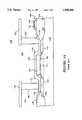
- FIG. 1Ais a cross-sectional view of a section of an integrated circuit device including an etch stop layer formed by conventional methods.
- FIG. 1Bis a top view of the integrated circuit section of FIG. 1A, without metallization layers 150, 152.
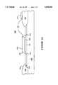
- FIGS. 2A-2Dare cross-sections of an integrated circuit device in various stages of fabrication by a process in accordance with the present invention.
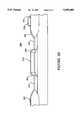
- FIG. 3is a flow chart representing the steps of a semiconductor fabrication process in accordance with the present invention.
- MOS device 100comprises a substrate 110 having a deposition layer 102 that has been doped to form a source 112 and drain 113. Lightly and heavily doped regions are indicated as n - and n + , respectively.
- a channel 111 between source 112 and drain 113may or may not be doped.
- a polysilicon gate 114is separated from channel 111 by a gate oxide region 120 of silicon dioxide, and a polysilicon interconnect 116 is shown extending over a field oxide region 122 of silicon dioxide.
- An insulating layer 140which is typically silicon dioxide, electrically isolates source 112, drain 113, gate 114, and interconnect 116 from metallization layers 150, 152 which couple device 100 into an integrated circuit through contacts 160, 162, respectively.
- Metal contact 162is shown misaligned so that it extends over field oxide region 122.
- Silicide layers 130, 132, 134, 136are included to enhance the conductivity of underlying source 112, drain 113, gate 114, and interconnect 116. Silicide layers 130, 132 also improve the electrical connections of source 112 and drain 113 with contacts 160, 162, respectively. Silicide layers 130, 132, 134, 136 are typically generated by depositing a silicide-forming refractory metal such as Ti over the exposed surfaces of deposition, oxide, and polysilicon layers 102, 104, 106, respectively, and annealing the coated structure. Annealing allows silicon in source 112, drain 113, gate 114, and interconnect 116 to migrate into the overlying refractory metal to form the corresponding refractory metal silicide layers 130, 132, 134, 136.
- a silicide-forming refractory metalsuch as Ti
- Annealingallows silicon in source 112, drain 113, gate 114, and interconnect 116 to migrate into the overlying refractory metal to form the corresponding
- the silicon in gate oxide 120 and field oxide 122does not migrate, leaving the overlying refractory metal unreacted through the annealing step. In conventional processes, this unreacted refractory metal is removed in a subsequent step and an etch stop such as silicon nitride layer 170 is deposited over the wafer.
- an etch stopsuch as silicon nitride layer 170 is deposited over the wafer.
- Insulator layer 140is deposited after silicon nitride layers 170, and selectively etched to prepare contact holes for electrical contacts 160, 162. If, as indicated in FIG. 1, the etched region extends beyond the edge of drain 113 silicon nitride layer 170 prevents etching of field oxide 120. Overetching may also occur at source 112 and at electrical contacts to gate 114 and interconnect 116 (the latter two contacts are not shown in FIG. 1A).
- FIG. 1Bthere is shown a top view of integrated circuit 100, indicating the location of sources 112, drains 113, gates 114, and contacts 160 for a series of devices 100.
- the position at which the cross-sectional view of FIG. 1A is takenis indicated by the arrows labeled A.
- each electrical contact 160, 162may lead to shorting if misaligned to impinge on a field oxide.
- Contacts 166 for gate 114may lead to similar shorts.
- FIGS. 2A-2Dthere are shown cross-sectional representations of a series of semiconductor structures 200, 240, 250, 260 at various stages of a fabrication process in accordance with the present invention.
- semiconductor structure 200following formation of diffusion layer 202, oxide layer 204, and polysilicon layer 206 over substrate 210.
- diffusion layer 202comprises source 212 and drain 213 formed by doping substrate 210 and (optionally) channel 211.
- Oxide layer 204is typically formed by the LOCOS process. This process is well known in semiconductor manufacturing and is not described in detail here.
- Gate oxide 220isolates channel 211 from polysilicon gate 214 and field oxide 222 isolates semiconductor structure 200 from other devices of the integrated circuit.
- Polysilicon layer 206comprises polysilicon gate 214 and polysilicon interconnect 216 over gate oxide 220 and field oxide 222, respectively. Diffusion, oxide, and polysilicon layers 202, 204, 206, respectively, may be produced by a number of different well-known processes.
- a semiconductor structure 240formed by depositing a silicide-forming refractory metal layer 242 over structure 200.
- refractory metal layer 242is deposited over unheated structure 200 by sputter deposition, although other deposition techniques may be used.
- the thickness of refractory metal layer 242is typically between 50 ⁇ and 1000 ⁇ , and, is preferably, in the range 200 ⁇ to 400 ⁇ .
- silicide-forming refractory metal layer 242is titanium.
- cobalt, hafnium, molybdenum, nickel, palladium, platinum, tantalum, tungsten, and zirconiummay also be used to form refractory metal layer 242.
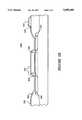
- FIG. 2Cthere is shown a semiconductor structure 250 formed by annealing structure 240 of FIG. 2B.
- annealingis typically done using rapid thermal processing techniques in which structure 240 is heated to temperatures between about 600° C. and about 800° C. for between about 10 and 60 seconds.
- Refractory metal silicide layers 230, 232, 234, 236are produced over source 212, drain 213, polysilicon gate 214, and polysilicon interconnect 216, respectively.
- Refractory metal layers 242 of FIG. 2B over gate and field oxides 220, 222remain unaffected, since silicon bound up in the silicon oxides of gate and field oxides 220, 222, does not react with refractory metal layer 242 under annealing conditions.
- FIG. 2Dthere is shown a semiconductor structure 260 formed by oxidizing semiconductor structure 250 of FIG. 2C.
- Refractory metal silicide layers 230, 232, 234, 236are unaffected by the oxidation, while refractory metal layer 242 of FIG. 2C is oxidized to form refractory metal oxide layer 262.
- Structure 250is oxidized by heating it to between 400° C. and 900° C. and exposing the heated structure 250 to an oxidizing agent under either wet or dry conditions. In the preferred embodiment, structure 250 is heated to between 500° C. and 600° C. and exposed to O 2 under wet conditions. The duration of the oxidation step depends on the thickness of the film. For a typical 300 ⁇ thick titanium metal layer 242, structure 250 is oxidized for approximately 10 to 15 minutes. Metal oxide layers 262 form an etch stop which is not attacked by contact etching in a subsequent step, protecting gate and field oxides 220, 222, respectively.
- step 310deposition, oxide, and polysilicon layers 202, 204, 206 of FIGS. 2A-2D are formed using well-known methods.
- a layer 242 of silicide-forming refractory metalis then deposited 320 over the exposed surfaces of deposition, oxide, and polysilicon layers 202, 204, 206 to form coated structure 240.
- Annealing 330 structure 240 following deposition 320 of the silicide-forming refractory metal layer 242produces refractory metal silicide layers 230, 232, 234, 236 over source 212, drain 213, polysilicon gate 214, and polysilicon interconnects 216, respectively.
- Oxidizing 340 unreacted refractory metal layer 242then forms refractory metal oxide layers 262 over gate and field oxides 220, 222.
- Refractory metal oxide layers 262act as an etch stop to prevent overetching of the underlying oxide layers.
- a method for forming etch stop layers over semiconductor structures without the need for additional etching, masking, and deposition stepshas been presented.
- a refractory metal capable of forming silicides and oxides under standard processing conditionsis deposited over the deposition, oxide, and polysilicon layers which define the gates, sources, drains and device structures of a MOS integrated circuit. Annealing forms refractory metal silicide layers over unoxidized silicon structures, and subsequent oxidation forms refractory metal oxide layers over silicon dioxide structures.
Landscapes
- Engineering & Computer Science (AREA)
- Manufacturing & Machinery (AREA)
- Computer Hardware Design (AREA)
- Microelectronics & Electronic Packaging (AREA)
- Power Engineering (AREA)
- Internal Circuitry In Semiconductor Integrated Circuit Devices (AREA)
- Electrodes Of Semiconductors (AREA)
Abstract
Description
Claims (10)
Priority Applications (1)
| Application Number | Priority Date | Filing Date | Title |
|---|---|---|---|
| US08/486,803US5698468A (en) | 1995-06-07 | 1995-06-07 | Silicidation process with etch stop |
Applications Claiming Priority (1)
| Application Number | Priority Date | Filing Date | Title |
|---|---|---|---|
| US08/486,803US5698468A (en) | 1995-06-07 | 1995-06-07 | Silicidation process with etch stop |
Publications (1)
| Publication Number | Publication Date |
|---|---|
| US5698468Atrue US5698468A (en) | 1997-12-16 |
Family
ID=23933305
Family Applications (1)
| Application Number | Title | Priority Date | Filing Date |
|---|---|---|---|
| US08/486,803Expired - LifetimeUS5698468A (en) | 1995-06-07 | 1995-06-07 | Silicidation process with etch stop |
Country Status (1)
| Country | Link |
|---|---|
| US (1) | US5698468A (en) |
Cited By (8)
| Publication number | Priority date | Publication date | Assignee | Title |
|---|---|---|---|---|
| US5780348A (en)* | 1997-07-14 | 1998-07-14 | United Microelectronics Corporation | Method of making a self-aligned silicide component |
| US6133122A (en)* | 1997-06-06 | 2000-10-17 | Nec Corporation | Method of fabricating semiconductor device for preventing rising-up of siliside |
| US6689702B2 (en)* | 1998-12-15 | 2004-02-10 | Intel Corporation | High dielectric constant metal oxide gate dielectrics |
| US20040039262A1 (en)* | 1999-06-03 | 2004-02-26 | Bardy Gust H. | System and method for providing feedback to an individual patient for automated remote patient care |
| US20060084275A1 (en)* | 2004-10-14 | 2006-04-20 | Young-Sub You | Etch stop structure and method of manufacture, and semiconductor device and method of manufacture |
| US20090317966A1 (en)* | 2008-06-17 | 2009-12-24 | Kouji Matsuo | Semiconductor device manufacturing method |
| US7745301B2 (en) | 2005-08-22 | 2010-06-29 | Terapede, Llc | Methods and apparatus for high-density chip connectivity |
| US8957511B2 (en) | 2005-08-22 | 2015-02-17 | Madhukar B. Vora | Apparatus and methods for high-density chip connectivity |
Citations (6)
| Publication number | Priority date | Publication date | Assignee | Title |
|---|---|---|---|---|
| US4881105A (en)* | 1988-06-13 | 1989-11-14 | International Business Machines Corporation | Integrated trench-transistor structure and fabrication process |
| US5223081A (en)* | 1991-07-03 | 1993-06-29 | Doan Trung T | Method for roughening a silicon or polysilicon surface for a semiconductor substrate |
| US5275715A (en)* | 1992-01-23 | 1994-01-04 | Micron Technology Inc. | Electroplating process for enhancing the conformality of titanium and titanium nitride films in the manufacture of integrated circuits and structures produced thereby |
| US5288666A (en)* | 1990-03-21 | 1994-02-22 | Ncr Corporation | Process for forming self-aligned titanium silicide by heating in an oxygen rich environment |
| US5316977A (en)* | 1991-07-16 | 1994-05-31 | Kabushiki Kaisha Toshiba | Method of manufacturing a semiconductor device comprising metal silicide |
| US5434096A (en)* | 1994-10-05 | 1995-07-18 | Taiwan Semiconductor Manufacturing Company Ltd. | Method to prevent silicide bubble in the VLSI process |
- 1995
- 1995-06-07USUS08/486,803patent/US5698468A/ennot_activeExpired - Lifetime
Patent Citations (6)
| Publication number | Priority date | Publication date | Assignee | Title |
|---|---|---|---|---|
| US4881105A (en)* | 1988-06-13 | 1989-11-14 | International Business Machines Corporation | Integrated trench-transistor structure and fabrication process |
| US5288666A (en)* | 1990-03-21 | 1994-02-22 | Ncr Corporation | Process for forming self-aligned titanium silicide by heating in an oxygen rich environment |
| US5223081A (en)* | 1991-07-03 | 1993-06-29 | Doan Trung T | Method for roughening a silicon or polysilicon surface for a semiconductor substrate |
| US5316977A (en)* | 1991-07-16 | 1994-05-31 | Kabushiki Kaisha Toshiba | Method of manufacturing a semiconductor device comprising metal silicide |
| US5275715A (en)* | 1992-01-23 | 1994-01-04 | Micron Technology Inc. | Electroplating process for enhancing the conformality of titanium and titanium nitride films in the manufacture of integrated circuits and structures produced thereby |
| US5434096A (en)* | 1994-10-05 | 1995-07-18 | Taiwan Semiconductor Manufacturing Company Ltd. | Method to prevent silicide bubble in the VLSI process |
Non-Patent Citations (2)
| Title |
|---|
| Wolf, Silicon Processing for the VLSI Era, vol. 2: Process Integration, Lattice Press, pp. 144 147, 1990.* |
| Wolf, Silicon Processing for the VLSI Era, vol. 2: Process Integration, Lattice Press, pp. 144-147, 1990. |
Cited By (14)
| Publication number | Priority date | Publication date | Assignee | Title |
|---|---|---|---|---|
| US6133122A (en)* | 1997-06-06 | 2000-10-17 | Nec Corporation | Method of fabricating semiconductor device for preventing rising-up of siliside |
| US5780348A (en)* | 1997-07-14 | 1998-07-14 | United Microelectronics Corporation | Method of making a self-aligned silicide component |
| US6689702B2 (en)* | 1998-12-15 | 2004-02-10 | Intel Corporation | High dielectric constant metal oxide gate dielectrics |
| US20050087820A1 (en)* | 1998-12-15 | 2005-04-28 | Gang Bai | High dielectric constant metal oxide gate dielectrics |
| US6998357B2 (en) | 1998-12-15 | 2006-02-14 | Intel Corporation | High dielectric constant metal oxide gate dielectrics |
| US20040039262A1 (en)* | 1999-06-03 | 2004-02-26 | Bardy Gust H. | System and method for providing feedback to an individual patient for automated remote patient care |
| US20060084275A1 (en)* | 2004-10-14 | 2006-04-20 | Young-Sub You | Etch stop structure and method of manufacture, and semiconductor device and method of manufacture |
| US7741222B2 (en)* | 2004-10-14 | 2010-06-22 | Samsung Electronics Co., Ltd. | Etch stop structure and method of manufacture, and semiconductor device and method of manufacture |
| US7745301B2 (en) | 2005-08-22 | 2010-06-29 | Terapede, Llc | Methods and apparatus for high-density chip connectivity |
| US8957511B2 (en) | 2005-08-22 | 2015-02-17 | Madhukar B. Vora | Apparatus and methods for high-density chip connectivity |
| US20090317966A1 (en)* | 2008-06-17 | 2009-12-24 | Kouji Matsuo | Semiconductor device manufacturing method |
| US7981795B2 (en)* | 2008-06-17 | 2011-07-19 | Kabushiki Kaisha Toshiba | Semiconductor device manufacturing method |
| US20110212589A1 (en)* | 2008-06-17 | 2011-09-01 | Kabushiki Kaisha Toshiba | Semiconductor device manufacturing method |
| US8486828B2 (en) | 2008-06-17 | 2013-07-16 | Kabushiki Kaisha Toshiba | Semiconductor device manufacturing method |
Similar Documents
| Publication | Publication Date | Title |
|---|---|---|
| US4392150A (en) | MOS Integrated circuit having refractory metal or metal silicide interconnect layer | |
| US4102733A (en) | Two and three mask process for IGFET fabrication | |
| KR0126906B1 (en) | How to form self-aligned cobalt silicides on MOS integrated circuits | |
| US5874353A (en) | Method of forming a self-aligned silicide device | |
| US5346836A (en) | Process for forming low resistance contacts between silicide areas and upper level polysilicon interconnects | |
| KR100302894B1 (en) | Integrated circuit structure with dual thickness cobalt silicide layers and method for its manufacture | |
| US4470189A (en) | Process for making polycide structures | |
| US5840624A (en) | Reduction of via over etching for borderless contacts | |
| US5838051A (en) | Tungsten policide contacts for semiconductor devices | |
| US4900257A (en) | Method of making a polycide gate using a titanium nitride capping layer | |
| JPH04233275A (en) | Interconnection structure of integrated strucutre | |
| GB2077993A (en) | Low sheet resistivity composite conductor gate MOS device | |
| US4933297A (en) | Method for etching windows having different depths | |
| US5911114A (en) | Method of simultaneous formation of salicide and local interconnects in an integrated circuit structure | |
| US5041394A (en) | Method for forming protective barrier on silicided regions | |
| US5698468A (en) | Silicidation process with etch stop | |
| JPH0837164A (en) | Manufacture of semiconductor device | |
| JPH11261063A (en) | Method for manufacturing semiconductor device | |
| JP3326088B2 (en) | Semiconductor device and manufacturing method thereof | |
| EP0589159B1 (en) | Method for contacting a semiconductor device | |
| JP3305490B2 (en) | Method for manufacturing semiconductor device | |
| JPH05166753A (en) | Barrier metal process for submicron contact | |
| US6756254B2 (en) | Integrated circuit having an antifuse and a method of manufacture | |
| KR100353525B1 (en) | Method for forming gate electrode in semiconductor device | |
| JPH0945908A (en) | Semiconductor device and its manufacture |
Legal Events
| Date | Code | Title | Description |
|---|---|---|---|
| AS | Assignment | Owner name:LSI LOGIC CORPORATION, CALIFORNIA Free format text:ASSIGNMENT OF ASSIGNORS INTEREST;ASSIGNOR:KAPOOR, ASHOK K.;REEL/FRAME:007529/0176 Effective date:19950606 | |
| STCF | Information on status: patent grant | Free format text:PATENTED CASE | |
| FEPP | Fee payment procedure | Free format text:PAYOR NUMBER ASSIGNED (ORIGINAL EVENT CODE: ASPN); ENTITY STATUS OF PATENT OWNER: LARGE ENTITY | |
| FPAY | Fee payment | Year of fee payment:4 | |
| FPAY | Fee payment | Year of fee payment:8 | |
| FEPP | Fee payment procedure | Free format text:PAYOR NUMBER ASSIGNED (ORIGINAL EVENT CODE: ASPN); ENTITY STATUS OF PATENT OWNER: LARGE ENTITY Free format text:PAYER NUMBER DE-ASSIGNED (ORIGINAL EVENT CODE: RMPN); ENTITY STATUS OF PATENT OWNER: LARGE ENTITY | |
| FPAY | Fee payment | Year of fee payment:12 | |
| AS | Assignment | Owner name:DEUTSCHE BANK AG NEW YORK BRANCH, AS COLLATERAL AG Free format text:PATENT SECURITY AGREEMENT;ASSIGNORS:LSI CORPORATION;AGERE SYSTEMS LLC;REEL/FRAME:032856/0031 Effective date:20140506 | |
| AS | Assignment | Owner name:LSI CORPORATION, CALIFORNIA Free format text:CHANGE OF NAME;ASSIGNOR:LSI LOGIC CORPORATION;REEL/FRAME:033102/0270 Effective date:20070406 | |
| AS | Assignment | Owner name:AVAGO TECHNOLOGIES GENERAL IP (SINGAPORE) PTE. LTD Free format text:ASSIGNMENT OF ASSIGNORS INTEREST;ASSIGNOR:LSI CORPORATION;REEL/FRAME:035390/0388 Effective date:20140814 | |
| AS | Assignment | Owner name:AGERE SYSTEMS LLC, PENNSYLVANIA Free format text:TERMINATION AND RELEASE OF SECURITY INTEREST IN PATENT RIGHTS (RELEASES RF 032856-0031);ASSIGNOR:DEUTSCHE BANK AG NEW YORK BRANCH, AS COLLATERAL AGENT;REEL/FRAME:037684/0039 Effective date:20160201 Owner name:LSI CORPORATION, CALIFORNIA Free format text:TERMINATION AND RELEASE OF SECURITY INTEREST IN PATENT RIGHTS (RELEASES RF 032856-0031);ASSIGNOR:DEUTSCHE BANK AG NEW YORK BRANCH, AS COLLATERAL AGENT;REEL/FRAME:037684/0039 Effective date:20160201 | |
| AS | Assignment | Owner name:BELL SEMICONDUCTOR, LLC, ILLINOIS Free format text:ASSIGNMENT OF ASSIGNORS INTEREST;ASSIGNORS:AVAGO TECHNOLOGIES GENERAL IP (SINGAPORE) PTE. LTD.;BROADCOM CORPORATION;REEL/FRAME:044886/0001 Effective date:20171208 | |
| AS | Assignment | Owner name:CORTLAND CAPITAL MARKET SERVICES LLC, AS COLLATERA Free format text:SECURITY INTEREST;ASSIGNORS:HILCO PATENT ACQUISITION 56, LLC;BELL SEMICONDUCTOR, LLC;BELL NORTHERN RESEARCH, LLC;REEL/FRAME:045216/0020 Effective date:20180124 | |
| AS | Assignment | Owner name:BELL NORTHERN RESEARCH, LLC, ILLINOIS Free format text:SECURITY INTEREST;ASSIGNOR:CORTLAND CAPITAL MARKET SERVICES LLC;REEL/FRAME:060885/0001 Effective date:20220401 Owner name:BELL SEMICONDUCTOR, LLC, ILLINOIS Free format text:SECURITY INTEREST;ASSIGNOR:CORTLAND CAPITAL MARKET SERVICES LLC;REEL/FRAME:060885/0001 Effective date:20220401 Owner name:HILCO PATENT ACQUISITION 56, LLC, ILLINOIS Free format text:SECURITY INTEREST;ASSIGNOR:CORTLAND CAPITAL MARKET SERVICES LLC;REEL/FRAME:060885/0001 Effective date:20220401 |