US5696666A - Low profile exposed die chip carrier package - Google Patents
Low profile exposed die chip carrier packageDownload PDFInfo
- Publication number
- US5696666A US5696666AUS08/540,995US54099595AUS5696666AUS 5696666 AUS5696666 AUS 5696666AUS 54099595 AUS54099595 AUS 54099595AUS 5696666 AUS5696666 AUS 5696666A
- Authority
- US
- United States
- Prior art keywords
- perimeter
- semiconductor die
- cavity opening
- pcb
- chip carrier
- Prior art date
- Legal status (The legal status is an assumption and is not a legal conclusion. Google has not performed a legal analysis and makes no representation as to the accuracy of the status listed.)
- Expired - Lifetime
Links
Images

Classifications
- H—ELECTRICITY
- H01—ELECTRIC ELEMENTS
- H01L—SEMICONDUCTOR DEVICES NOT COVERED BY CLASS H10
- H01L23/00—Details of semiconductor or other solid state devices
- H01L23/48—Arrangements for conducting electric current to or from the solid state body in operation, e.g. leads, terminal arrangements ; Selection of materials therefor
- H01L23/488—Arrangements for conducting electric current to or from the solid state body in operation, e.g. leads, terminal arrangements ; Selection of materials therefor consisting of soldered or bonded constructions
- H01L23/498—Leads, i.e. metallisations or lead-frames on insulating substrates, e.g. chip carriers
- H01L23/49811—Additional leads joined to the metallisation on the insulating substrate, e.g. pins, bumps, wires, flat leads
- H01L23/49816—Spherical bumps on the substrate for external connection, e.g. ball grid arrays [BGA]
- H—ELECTRICITY
- H01—ELECTRIC ELEMENTS
- H01L—SEMICONDUCTOR DEVICES NOT COVERED BY CLASS H10
- H01L23/00—Details of semiconductor or other solid state devices
- H01L23/12—Mountings, e.g. non-detachable insulating substrates
- H01L23/13—Mountings, e.g. non-detachable insulating substrates characterised by the shape
- H—ELECTRICITY
- H01—ELECTRIC ELEMENTS
- H01L—SEMICONDUCTOR DEVICES NOT COVERED BY CLASS H10
- H01L23/00—Details of semiconductor or other solid state devices
- H01L23/28—Encapsulations, e.g. encapsulating layers, coatings, e.g. for protection
- H01L23/31—Encapsulations, e.g. encapsulating layers, coatings, e.g. for protection characterised by the arrangement or shape
- H01L23/3107—Encapsulations, e.g. encapsulating layers, coatings, e.g. for protection characterised by the arrangement or shape the device being completely enclosed
- H01L23/3121—Encapsulations, e.g. encapsulating layers, coatings, e.g. for protection characterised by the arrangement or shape the device being completely enclosed a substrate forming part of the encapsulation
- H01L23/3128—Encapsulations, e.g. encapsulating layers, coatings, e.g. for protection characterised by the arrangement or shape the device being completely enclosed a substrate forming part of the encapsulation the substrate having spherical bumps for external connection
- H—ELECTRICITY
- H01—ELECTRIC ELEMENTS
- H01L—SEMICONDUCTOR DEVICES NOT COVERED BY CLASS H10
- H01L2224/00—Indexing scheme for arrangements for connecting or disconnecting semiconductor or solid-state bodies and methods related thereto as covered by H01L24/00
- H01L2224/01—Means for bonding being attached to, or being formed on, the surface to be connected, e.g. chip-to-package, die-attach, "first-level" interconnects; Manufacturing methods related thereto
- H01L2224/42—Wire connectors; Manufacturing methods related thereto
- H01L2224/47—Structure, shape, material or disposition of the wire connectors after the connecting process
- H01L2224/48—Structure, shape, material or disposition of the wire connectors after the connecting process of an individual wire connector
- H01L2224/4805—Shape
- H01L2224/4809—Loop shape
- H01L2224/48091—Arched
- H—ELECTRICITY
- H01—ELECTRIC ELEMENTS
- H01L—SEMICONDUCTOR DEVICES NOT COVERED BY CLASS H10
- H01L2224/00—Indexing scheme for arrangements for connecting or disconnecting semiconductor or solid-state bodies and methods related thereto as covered by H01L24/00
- H01L2224/01—Means for bonding being attached to, or being formed on, the surface to be connected, e.g. chip-to-package, die-attach, "first-level" interconnects; Manufacturing methods related thereto
- H01L2224/42—Wire connectors; Manufacturing methods related thereto
- H01L2224/47—Structure, shape, material or disposition of the wire connectors after the connecting process
- H01L2224/48—Structure, shape, material or disposition of the wire connectors after the connecting process of an individual wire connector
- H01L2224/481—Disposition
- H01L2224/48151—Connecting between a semiconductor or solid-state body and an item not being a semiconductor or solid-state body, e.g. chip-to-substrate, chip-to-passive
- H01L2224/48221—Connecting between a semiconductor or solid-state body and an item not being a semiconductor or solid-state body, e.g. chip-to-substrate, chip-to-passive the body and the item being stacked
- H01L2224/48225—Connecting between a semiconductor or solid-state body and an item not being a semiconductor or solid-state body, e.g. chip-to-substrate, chip-to-passive the body and the item being stacked the item being non-metallic, e.g. insulating substrate with or without metallisation
- H01L2224/48227—Connecting between a semiconductor or solid-state body and an item not being a semiconductor or solid-state body, e.g. chip-to-substrate, chip-to-passive the body and the item being stacked the item being non-metallic, e.g. insulating substrate with or without metallisation connecting the wire to a bond pad of the item
- H—ELECTRICITY
- H01—ELECTRIC ELEMENTS
- H01L—SEMICONDUCTOR DEVICES NOT COVERED BY CLASS H10
- H01L2224/00—Indexing scheme for arrangements for connecting or disconnecting semiconductor or solid-state bodies and methods related thereto as covered by H01L24/00
- H01L2224/01—Means for bonding being attached to, or being formed on, the surface to be connected, e.g. chip-to-package, die-attach, "first-level" interconnects; Manufacturing methods related thereto
- H01L2224/42—Wire connectors; Manufacturing methods related thereto
- H01L2224/47—Structure, shape, material or disposition of the wire connectors after the connecting process
- H01L2224/48—Structure, shape, material or disposition of the wire connectors after the connecting process of an individual wire connector
- H01L2224/484—Connecting portions
- H01L2224/48463—Connecting portions the connecting portion on the bonding area of the semiconductor or solid-state body being a ball bond
- H01L2224/48465—Connecting portions the connecting portion on the bonding area of the semiconductor or solid-state body being a ball bond the other connecting portion not on the bonding area being a wedge bond, i.e. ball-to-wedge, regular stitch
- H—ELECTRICITY
- H01—ELECTRIC ELEMENTS
- H01L—SEMICONDUCTOR DEVICES NOT COVERED BY CLASS H10
- H01L24/00—Arrangements for connecting or disconnecting semiconductor or solid-state bodies; Methods or apparatus related thereto
- H01L24/01—Means for bonding being attached to, or being formed on, the surface to be connected, e.g. chip-to-package, die-attach, "first-level" interconnects; Manufacturing methods related thereto
- H01L24/42—Wire connectors; Manufacturing methods related thereto
- H01L24/47—Structure, shape, material or disposition of the wire connectors after the connecting process
- H01L24/48—Structure, shape, material or disposition of the wire connectors after the connecting process of an individual wire connector
- H—ELECTRICITY
- H01—ELECTRIC ELEMENTS
- H01L—SEMICONDUCTOR DEVICES NOT COVERED BY CLASS H10
- H01L2924/00—Indexing scheme for arrangements or methods for connecting or disconnecting semiconductor or solid-state bodies as covered by H01L24/00
- H01L2924/0001—Technical content checked by a classifier
- H01L2924/00014—Technical content checked by a classifier the subject-matter covered by the group, the symbol of which is combined with the symbol of this group, being disclosed without further technical details
- H—ELECTRICITY
- H01—ELECTRIC ELEMENTS
- H01L—SEMICONDUCTOR DEVICES NOT COVERED BY CLASS H10
- H01L2924/00—Indexing scheme for arrangements or methods for connecting or disconnecting semiconductor or solid-state bodies as covered by H01L24/00
- H01L2924/01—Chemical elements
- H01L2924/01013—Aluminum [Al]
- H—ELECTRICITY
- H01—ELECTRIC ELEMENTS
- H01L—SEMICONDUCTOR DEVICES NOT COVERED BY CLASS H10
- H01L2924/00—Indexing scheme for arrangements or methods for connecting or disconnecting semiconductor or solid-state bodies as covered by H01L24/00
- H01L2924/10—Details of semiconductor or other solid state devices to be connected
- H01L2924/11—Device type
- H01L2924/14—Integrated circuits
- H—ELECTRICITY
- H01—ELECTRIC ELEMENTS
- H01L—SEMICONDUCTOR DEVICES NOT COVERED BY CLASS H10
- H01L2924/00—Indexing scheme for arrangements or methods for connecting or disconnecting semiconductor or solid-state bodies as covered by H01L24/00
- H01L2924/15—Details of package parts other than the semiconductor or other solid state devices to be connected
- H01L2924/151—Die mounting substrate
- H01L2924/1515—Shape
- H01L2924/15151—Shape the die mounting substrate comprising an aperture, e.g. for underfilling, outgassing, window type wire connections
- H—ELECTRICITY
- H01—ELECTRIC ELEMENTS
- H01L—SEMICONDUCTOR DEVICES NOT COVERED BY CLASS H10
- H01L2924/00—Indexing scheme for arrangements or methods for connecting or disconnecting semiconductor or solid-state bodies as covered by H01L24/00
- H01L2924/15—Details of package parts other than the semiconductor or other solid state devices to be connected
- H01L2924/151—Die mounting substrate
- H01L2924/153—Connection portion
- H01L2924/1531—Connection portion the connection portion being formed only on the surface of the substrate opposite to the die mounting surface
- H01L2924/15311—Connection portion the connection portion being formed only on the surface of the substrate opposite to the die mounting surface being a ball array, e.g. BGA
- H—ELECTRICITY
- H01—ELECTRIC ELEMENTS
- H01L—SEMICONDUCTOR DEVICES NOT COVERED BY CLASS H10
- H01L2924/00—Indexing scheme for arrangements or methods for connecting or disconnecting semiconductor or solid-state bodies as covered by H01L24/00
- H01L2924/15—Details of package parts other than the semiconductor or other solid state devices to be connected
- H01L2924/181—Encapsulation
- H01L2924/1815—Shape
- H01L2924/1816—Exposing the passive side of the semiconductor or solid-state body
- H01L2924/18165—Exposing the passive side of the semiconductor or solid-state body of a wire bonded chip
Definitions
- This inventionrelates to printed circuit board chip carriers, and more particularly to overmolded and glob top chip carriers that provide for moisture relief.
- Plastic Ball Grid Array (PBGA) chip carrierssuch as the Over Molded Pad Array Carrier (OMPACTM), the Over Molded Peripheral Chip Carrier (OMPCC), and the Over Molded Pin Grid Array (OMPGA) and their equivalent glob top printed circuit board (PCB) chip carriers are susceptible to moisture absorption. When subjected to heat, these integrated circuit packages suffer from a well-known phenomenon called "popcorning.” This problem is particularly noticeable in surface mount packages using PCB substrates; they experience thermal and mechanical stresses due to exposure of the entire package to solder reflow temperatures. Typically, PCB packages must be baked prior to solder assembly to remove moisture.
- OMPACTMOver Molded Pad Array Carrier
- OMPCCOver Molded Peripheral Chip Carrier
- OMPGAOver Molded Pin Grid Array
- PCBprinted circuit board
- the die attach adhesiveis usually a hygroscopic material. When the package is exposed to solder reflow temperatures after the die attach adhesive has absorbed moisture, the moisture is rapidly converted into a gas, expanding dramatically. This causes the die to delaminate from the substrate, creating the "popcorn" effect.
- U.S. Pat. No. 4,866,506 by Nambu et. al.discusses a flat plastic-sealed lead frame package that has an opening on an underside of the package, allowing the die flag to be exposed to the atmosphere, thereby venting or releasing moisture when subjected to heat.
- This packagealso known as the Quad Flat Pack (QFP)
- QFPQuad Flat Pack
- the QFPdoes not use a substrate or PCB as in OMPAC, OMPCC, and OMPGA and their equivalents; thus, a different solution is required.
- U.S. Pat. No. 5,296,738 by Freyman et. al.discusses a PCB chip carrier with an opening(s) in the PCB substrate, located directly beneath the semiconductor die, which provides the means for moisture relief when the package is subjected to extreme temperature excursions (e.g., board reflow profiles).
- the openingis initially covered on the back side of the PCB substrate with solder resist.
- the covered openingprevents the flow of die attach material from the top side surface, through the opening, on to the back side solder pads; however, the opening(s) are partially or completely filled with die attach material.
- the solder resistAfter final assembly of the package, the solder resist must be pierced or punctured to create the final opening for moisture relief.
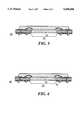
- FIG. 1is a cut view of an overmolded pad grid array chip carrier in accordance with the present invention.
- FIG. 2is an exploded view showing the bottom surfaces of an overmolded pad grid array chip carrier in accordance with the present invention.
- FIG. 3is a cut view of an overmolded pad grid array chip carrier in accordance with the present invention.
- FIG. 4is a cut view of an overmolded pad grid array chip carrier in accordance with the present invention.
- An integrated circuit (IC) packagehas a semiconductor die mounted in a printed circuit substrate.
- the substratehas a through-cavity opening with a perimeter which is substantially the same shape and size as the die perimeter.
- through-cavity openingdescribes a rectangular-shaped opening in the center of the substrate which extends completely through the substrate.
- the dieis seated in the through-cavity opening such that the bottom surface of the die is substantially coplanar with the bottom side of the substrate.
- the typical die-to-substrate die attach interfaceis eliminated, leaving the back surface of the die exposed to the atmosphere. Die attach material is no longer needed, since it is not necessary to mount the die on to a substrate.
- the packageis less susceptible to the effects of moisture absorption, as the hygroscopic die attach material is eliminated.
- heat generated by the diewhich must typically be drawn from the chip through package interconnects and added heat sinks, is more directly and efficiently dissipated.
- An overmolded or glob top materialencapsulates the top surface of the die and portions of the substrate top side. The die is held in place by direct and intimate contact between the through-cavity opening perimeter and the die perimeter, and encapsulant-to-die adhesion.
- the thickness of the chipcan be virtually eliminated as a factor, since the top surface of the die is at approximately the same level as the top side of the substrate.
- Lower wire bond loop heightsalso contribute to reduction in package height profile, due to the lower level of the die. Therefore, an additional benefit of the present invention is that it results in a significantly reduced package profile.
- the chip carriermay take the form of an overmolded pad array carrier, an over molded pin grid array, an overmolded peripheral chip carrier, or alternatively, a glob top pad array carrier, a glob top pin grid array or a glob top peripheral array chip carrier.
- overmolded and glob top carriersalso known as BGA or PBGA carriers, are found in the following U.S. Pat. Nos. incorporated herein by reference: 5,241,133; 4,688,152; 5,239,198 and 5,296,738.
- the present inventionis applicable to any printed circuit substrate chip carrier incorporating a leadless peripheral interconnect design, and having integrated circuits and an encapsulant such as an overmold or glob top.
- a printed circuit board (PCB) for receiving an IChas printed circuitry 18 on the top side of the PCB.
- the present inventionemploys a through-cavity opening 22, extending completely through the PCB 14, for die mounting.
- the perimeter of the die 12is in direct and intimate contact with the perimeter of the through-cavity opening 22.
- a package 30where the substrate through-cavity opening 23 perimeter is slightly larger than the die 12 perimeter, and the gap between the two perimeters is filled with encapsulant to provide additional mechanical support for the die.
- a package 40where an adhesive material 42 is employed between the perimeter of the die 12 and the through-cavity opening 23, prior to encapsulation, to hold the die in place during wire bonding and encapsulation, and to provide mechanical support of the die in the assembled package.
- the semiconductor die 12is placed, bottom surface facing down, into the PCB through-cavity opening 22. Contrary to the processes of the prior art, the die is not placed onto a PCB surface and held in place with a die attach adhesive. Instead, the die is held in place by the temporary application of a vacuum which is drawn on the bottom surface of the chip. The die 12 is then wire bonded using conventional wire bonding techniques, as the die is firmly held in place by the vacuum. When wire bonding is complete, the vacuum is removed and the die remains in place by virtue of the wire bonds 26 that have been made between the die 12 and the PCB 14. The die 12 is connected to the surface mount solder pads 24 by means of vias 20 through the printed circuit substrate 14.
- a plastic resinsuch as a glob top or transfer-molded encapsulant 16 is applied over the die 12 and portions of the substrate 14 forming the PBGA chip carrier 10 shown in FIG. 1.
- the perimeter portion of the top side of the substrateis not covered by the encapsulating resin.
- the bottom side of the PCB substrateis not covered with encapsulant.
- adhesive bondsare formed at the encapsulant-to-die interfaces, providing mechanical support for the chip. As shown in FIG.
- a perimeter or peripheral chip carriertypically has surface mount solder pads 24 on the back side of the PCB substrate located in array format, but only in 3 to 4 rows around the perimeter of the package, leaving the center of the package free of solder interconnection sites. Therefore, a through-cavity opening in the center of the package substrate does not affect the pin count of peripheral PBGA packages.
- the PBGA packagemay be furnished with bare solder pads 24, or as illustrated in FIG. 1, the solder pads may optionally have solder balls or bumps 13.
- FIG. 3there is shown another cut view of a leadless overmolded peripheral PBGA package in accordance with the present invention.
- This version of a PBGA carrier 30has a through-cavity opening 23 perimeter which is slightly larger than the die 12 perimeter.
- Plastic resin encapsulant 16fills the void between the die 12 perimeter and the through-cavity opening 23 perimeter. Compressive forces, resulting from slight shrinkage of the encapsulant as it is cooled down to room temperature, are applied against the perimeter of the die, providing additional mechanical support.
- FIG. 4there is shown another cut view of a leadless overmolded peripheral PBGA package in accordance with the present invention.
- This version of a PBGA carrier 40also has a through cavity opening 23 perimeter which is slightly larger than the die 12 perimeter.
- an adhesive material 42is applied between the through-cavity opening perimeter and the die perimeter. The adhesive provides support for the chip during wire bonding and encapsulation, and continues to provide mechanical support in the finished package.
- the present inventionprovides for a novel means of moisture relief for plastic encapsulated peripheral pad chip carriers made from printed circuit substrates.
- the dieis mounted in a through-cavity opening in the substrate, and is held in place by wire bonds and the adhesive strength of the encapsulant at the encapsulant-to-die interface.
- additional mechanical support of the ICis supplied by direct and intimate contact between the IC perimeter and the through-cavity opening perimeter, or alternatively, by an encapsulant or adhesive between the IC perimeter and the through-cavity opening perimeter.
- the elimination of the hygroscopic die attach materialremoves the one component that is most responsible for moisture absorption, thereby providing a package that is more stable in humid environments and that is more amenable to automated assembly. Additional benefits which result from the present invention include: more efficient thermal dissipation from the die and a greatly reduced package height profile.
Landscapes
- Engineering & Computer Science (AREA)
- Microelectronics & Electronic Packaging (AREA)
- Physics & Mathematics (AREA)
- Condensed Matter Physics & Semiconductors (AREA)
- General Physics & Mathematics (AREA)
- Computer Hardware Design (AREA)
- Power Engineering (AREA)
- Structures Or Materials For Encapsulating Or Coating Semiconductor Devices Or Solid State Devices (AREA)
Abstract
Description
Claims (15)
Priority Applications (1)
| Application Number | Priority Date | Filing Date | Title |
|---|---|---|---|
| US08/540,995US5696666A (en) | 1995-10-11 | 1995-10-11 | Low profile exposed die chip carrier package |
Applications Claiming Priority (1)
| Application Number | Priority Date | Filing Date | Title |
|---|---|---|---|
| US08/540,995US5696666A (en) | 1995-10-11 | 1995-10-11 | Low profile exposed die chip carrier package |
Publications (1)
| Publication Number | Publication Date |
|---|---|
| US5696666Atrue US5696666A (en) | 1997-12-09 |
Family
ID=24157764
Family Applications (1)
| Application Number | Title | Priority Date | Filing Date |
|---|---|---|---|
| US08/540,995Expired - LifetimeUS5696666A (en) | 1995-10-11 | 1995-10-11 | Low profile exposed die chip carrier package |
Country Status (1)
| Country | Link |
|---|---|
| US (1) | US5696666A (en) |
Cited By (180)
| Publication number | Priority date | Publication date | Assignee | Title |
|---|---|---|---|---|
| WO1999044233A1 (en)* | 1998-02-24 | 1999-09-02 | Micron Technology, Inc. | Low profile ball grid array package |
| US6111324A (en)* | 1998-02-05 | 2000-08-29 | Asat, Limited | Integrated carrier ring/stiffener and method for manufacturing a flexible integrated circuit package |
| US6117710A (en)* | 1997-02-11 | 2000-09-12 | National Semiconductor Corporation | Plastic package with exposed die and method of making same |
| US6163069A (en)* | 1997-10-09 | 2000-12-19 | Mitsubishi Denki Kabushiki Kaisha | Semiconductor device having pads for connecting a semiconducting element to a mother board |
| US6201302B1 (en)* | 1998-12-31 | 2001-03-13 | Sampo Semiconductor Corporation | Semiconductor package having multi-dies |
| US6229200B1 (en) | 1998-06-10 | 2001-05-08 | Asat Limited | Saw-singulated leadless plastic chip carrier |
| US6333566B1 (en)* | 1999-03-26 | 2001-12-25 | Oki Electric Industry Co., Ltd. | Semiconductor having high density packaging thereof |
| US20020020898A1 (en)* | 2000-08-16 | 2002-02-21 | Vu Quat T. | Microelectronic substrates with integrated devices |
| US20020020907A1 (en)* | 2000-03-25 | 2002-02-21 | Amkor Technology, Inc. | Semiconductor package |
| US20020070443A1 (en)* | 2000-12-08 | 2002-06-13 | Xiao-Chun Mu | Microelectronic package having an integrated heat sink and build-up layers |
| US20020093093A1 (en)* | 2001-01-15 | 2002-07-18 | Jong Sik Paek | Semiconductor package with stacked dies |
| US20020093087A1 (en)* | 2001-01-15 | 2002-07-18 | Paek Jong Sik | Semiconductor package with stacked dies |
| US6433277B1 (en) | 1998-06-24 | 2002-08-13 | Amkor Technology, Inc. | Plastic integrated circuit package and method and leadframe for making the package |
| US6448633B1 (en) | 1998-11-20 | 2002-09-10 | Amkor Technology, Inc. | Semiconductor package and method of making using leadframe having lead locks to secure leads to encapsulant |
| US6455356B1 (en) | 1998-10-21 | 2002-09-24 | Amkor Technology | Methods for moding a leadframe in plastic integrated circuit devices |
| US6476478B1 (en) | 1999-11-12 | 2002-11-05 | Amkor Technology, Inc. | Cavity semiconductor package with exposed leads and die pad |
| US6501184B1 (en) | 1999-05-20 | 2002-12-31 | Amkor Technology, Inc. | Semiconductor package and method for manufacturing the same |
| US6512288B1 (en) | 1999-06-07 | 2003-01-28 | Amkor Technology, Inc. | Circuit board semiconductor package |
| US6515356B1 (en) | 1999-05-07 | 2003-02-04 | Amkor Technology, Inc. | Semiconductor package and method for fabricating the same |
| US20030043557A1 (en)* | 2001-08-31 | 2003-03-06 | Martinez Paul Aurelio | System and method for reducing apparent height of a board system |
| US6537848B2 (en) | 2001-05-30 | 2003-03-25 | St. Assembly Test Services Ltd. | Super thin/super thermal ball grid array package |
| US6576998B1 (en) | 2002-02-28 | 2003-06-10 | Amkor Technology, Inc. | Thin semiconductor package with semiconductor chip and electronic discrete device |
| KR100388290B1 (en)* | 1999-12-10 | 2003-06-19 | 앰코 테크놀로지 코리아 주식회사 | semiconductor package and its manufacturing method |
| US6605865B2 (en) | 2001-03-19 | 2003-08-12 | Amkor Technology, Inc. | Semiconductor package with optimized leadframe bonding strength |
| US6608366B1 (en) | 2002-04-15 | 2003-08-19 | Harry J. Fogelson | Lead frame with plated end leads |
| US6611047B2 (en) | 2001-10-12 | 2003-08-26 | Amkor Technology, Inc. | Semiconductor package with singulation crease |
| EP1189273A3 (en)* | 2000-09-14 | 2003-08-27 | Shinko Electric Industries Co. Ltd. | Semiconductor device and production process |
| US6627977B1 (en) | 2002-05-09 | 2003-09-30 | Amkor Technology, Inc. | Semiconductor package including isolated ring structure |
| US6636334B2 (en)* | 1999-03-26 | 2003-10-21 | Oki Electric Industry Co., Ltd. | Semiconductor device having high-density packaging thereof |
| US6670222B1 (en) | 1997-06-14 | 2003-12-30 | Jds Uniphase Corporation | Texturing of a die pad surface for enhancing bonding strength in the surface attachment |
| US20040014258A1 (en)* | 1999-03-26 | 2004-01-22 | Akio Nakamura | Semiconductor device and method of fabricating the same |
| US6700187B2 (en) | 2001-03-27 | 2004-03-02 | Amkor Technology, Inc. | Semiconductor package and method for manufacturing the same |
| US6713322B2 (en) | 2001-03-27 | 2004-03-30 | Amkor Technology, Inc. | Lead frame for semiconductor package |
| US6734534B1 (en)* | 2000-08-16 | 2004-05-11 | Intel Corporation | Microelectronic substrate with integrated devices |
| US6750545B1 (en) | 2003-02-28 | 2004-06-15 | Amkor Technology, Inc. | Semiconductor package capable of die stacking |
| US6756658B1 (en) | 2001-04-06 | 2004-06-29 | Amkor Technology, Inc. | Making two lead surface mounting high power microleadframe semiconductor packages |
| US6759737B2 (en) | 2000-03-25 | 2004-07-06 | Amkor Technology, Inc. | Semiconductor package including stacked chips with aligned input/output pads |
| US6762078B2 (en) | 1999-05-20 | 2004-07-13 | Amkor Technology, Inc. | Semiconductor package having semiconductor chip within central aperture of substrate |
| US6777789B1 (en) | 2001-03-20 | 2004-08-17 | Amkor Technology, Inc. | Mounting for a package containing a chip |
| US6794740B1 (en) | 2003-03-13 | 2004-09-21 | Amkor Technology, Inc. | Leadframe package for semiconductor devices |
| US6798047B1 (en) | 2002-12-26 | 2004-09-28 | Amkor Technology, Inc. | Pre-molded leadframe |
| US6798046B1 (en) | 2002-01-22 | 2004-09-28 | Amkor Technology, Inc. | Semiconductor package including ring structure connected to leads with vertically downset inner ends |
| US6803645B2 (en) | 2000-12-29 | 2004-10-12 | Amkor Technology, Inc. | Semiconductor package including flip chip |
| US20040212081A1 (en)* | 2003-04-08 | 2004-10-28 | Carberry Patrick J. | Process for fabricating a power hybrid module |
| US6818973B1 (en) | 2002-09-09 | 2004-11-16 | Amkor Technology, Inc. | Exposed lead QFP package fabricated through the use of a partial saw process |
| US6833619B1 (en) | 2003-04-28 | 2004-12-21 | Amkor Technology, Inc. | Thin profile semiconductor package which reduces warpage and damage during laser markings |
| US6841414B1 (en) | 2002-06-19 | 2005-01-11 | Amkor Technology, Inc. | Saw and etch singulation method for a chip package |
| US6847103B1 (en) | 1999-11-09 | 2005-01-25 | Amkor Technology, Inc. | Semiconductor package with exposed die pad and body-locking leadframe |
| US6867071B1 (en) | 2002-07-12 | 2005-03-15 | Amkor Technology, Inc. | Leadframe including corner leads and semiconductor package using same |
| US6873041B1 (en) | 2001-11-07 | 2005-03-29 | Amkor Technology, Inc. | Power semiconductor package with strap |
| US6879034B1 (en) | 2003-05-01 | 2005-04-12 | Amkor Technology, Inc. | Semiconductor package including low temperature co-fired ceramic substrate |
| US6885086B1 (en) | 2002-03-05 | 2005-04-26 | Amkor Technology, Inc. | Reduced copper lead frame for saw-singulated chip package |
| US6893900B1 (en) | 1998-06-24 | 2005-05-17 | Amkor Technology, Inc. | Method of making an integrated circuit package |
| US6897550B1 (en) | 2003-06-11 | 2005-05-24 | Amkor Technology, Inc. | Fully-molded leadframe stand-off feature |
| US6919620B1 (en) | 2002-09-17 | 2005-07-19 | Amkor Technology, Inc. | Compact flash memory card with clamshell leadframe |
| US6921967B2 (en) | 2003-09-24 | 2005-07-26 | Amkor Technology, Inc. | Reinforced die pad support structure |
| US6927483B1 (en) | 2003-03-07 | 2005-08-09 | Amkor Technology, Inc. | Semiconductor package exhibiting efficient lead placement |
| US20050197983A1 (en)* | 2000-07-04 | 2005-09-08 | Jun Tani | Information processing apparatus and method, and recording medium |
| US6965159B1 (en) | 2001-09-19 | 2005-11-15 | Amkor Technology, Inc. | Reinforced lead-frame assembly for interconnecting circuits within a circuit module |
| US6967395B1 (en) | 2001-03-20 | 2005-11-22 | Amkor Technology, Inc. | Mounting for a package containing a chip |
| US6982488B2 (en) | 1999-08-24 | 2006-01-03 | Amkor Technology, Inc. | Semiconductor package and method for fabricating the same |
| US7001799B1 (en) | 2003-03-13 | 2006-02-21 | Amkor Technology, Inc. | Method of making a leadframe for semiconductor devices |
| US7005326B1 (en) | 1998-06-24 | 2006-02-28 | Amkor Technology, Inc. | Method of making an integrated circuit package |
| US7009296B1 (en) | 2004-01-15 | 2006-03-07 | Amkor Technology, Inc. | Semiconductor package with substrate coupled to a peripheral side surface of a semiconductor die |
| US7008825B1 (en) | 2003-05-27 | 2006-03-07 | Amkor Technology, Inc. | Leadframe strip having enhanced testability |
| US7030474B1 (en) | 1998-06-24 | 2006-04-18 | Amkor Technology, Inc. | Plastic integrated circuit package and method and leadframe for making the package |
| US7033517B1 (en) | 2003-09-15 | 2006-04-25 | Asat Ltd. | Method of fabricating a leadless plastic chip carrier |
| US7042068B2 (en) | 2000-04-27 | 2006-05-09 | Amkor Technology, Inc. | Leadframe and semiconductor package made using the leadframe |
| US7045883B1 (en) | 2001-04-04 | 2006-05-16 | Amkor Technology, Inc. | Thermally enhanced chip scale lead on chip semiconductor package and method of making same |
| US7045396B2 (en) | 1999-12-16 | 2006-05-16 | Amkor Technology, Inc. | Stackable semiconductor package and method for manufacturing same |
| US20060103010A1 (en)* | 2004-11-12 | 2006-05-18 | Stats Chippac Ltd. | Semiconductor package system with substrate heat sink |
| US7057268B1 (en) | 2004-01-27 | 2006-06-06 | Amkor Technology, Inc. | Cavity case with clip/plug for use on multi-media card |
| US7064009B1 (en) | 2001-04-04 | 2006-06-20 | Amkor Technology, Inc. | Thermally enhanced chip scale lead on chip semiconductor package and method of making same |
| US20060131729A1 (en)* | 2004-12-17 | 2006-06-22 | Samsung Electro-Mechanics Co., Ltd. | Ball grid array substrate having window and method of fabricating same |
| US7067908B2 (en) | 1999-10-15 | 2006-06-27 | Amkor Technology, Inc. | Semiconductor package having improved adhesiveness and ground bonding |
| US7071541B1 (en) | 1998-06-24 | 2006-07-04 | Amkor Technology, Inc. | Plastic integrated circuit package and method and leadframe for making the package |
| US20060154403A1 (en)* | 2005-01-12 | 2006-07-13 | Mclellan Neil | Thin array plastic package without die attach pad and process for fabricating the same |
| US7091594B1 (en) | 2004-01-28 | 2006-08-15 | Amkor Technology, Inc. | Leadframe type semiconductor package having reduced inductance and its manufacturing method |
| US7091581B1 (en) | 2004-06-14 | 2006-08-15 | Asat Limited | Integrated circuit package and process for fabricating the same |
| US7095103B1 (en) | 2003-05-01 | 2006-08-22 | Amkor Technology, Inc. | Leadframe based memory card |
| US7102208B1 (en) | 1999-10-15 | 2006-09-05 | Amkor Technology, Inc. | Leadframe and semiconductor package with improved solder joint strength |
| US7112474B1 (en) | 1998-06-24 | 2006-09-26 | Amkor Technology, Inc. | Method of making an integrated circuit package |
| US7115445B2 (en) | 1999-10-15 | 2006-10-03 | Amkor Technology, Inc. | Semiconductor package having reduced thickness |
| US7138707B1 (en) | 2003-10-21 | 2006-11-21 | Amkor Technology, Inc. | Semiconductor package including leads and conductive posts for providing increased functionality |
| US20070035008A1 (en)* | 2005-08-09 | 2007-02-15 | Chipmos Technologies (Bermuda) Ltd. Chipmos Technologies Inc. | Thin IC package for improving heat dissipation from chip backside |
| US7190062B1 (en) | 2004-06-15 | 2007-03-13 | Amkor Technology, Inc. | Embedded leadframe semiconductor package |
| US7192807B1 (en) | 2002-11-08 | 2007-03-20 | Amkor Technology, Inc. | Wafer level package and fabrication method |
| US7202554B1 (en) | 2004-08-19 | 2007-04-10 | Amkor Technology, Inc. | Semiconductor package and its manufacturing method |
| US7211879B1 (en) | 2003-11-12 | 2007-05-01 | Amkor Technology, Inc. | Semiconductor package with chamfered corners and method of manufacturing the same |
| US7214326B1 (en) | 2003-11-07 | 2007-05-08 | Amkor Technology, Inc. | Increased capacity leadframe and semiconductor package using the same |
| US7217991B1 (en) | 2004-10-22 | 2007-05-15 | Amkor Technology, Inc. | Fan-in leadframe semiconductor package |
| US20070145548A1 (en)* | 2003-12-22 | 2007-06-28 | Amkor Technology, Inc. | Stack-type semiconductor package and manufacturing method thereof |
| US7245007B1 (en) | 2003-09-18 | 2007-07-17 | Amkor Technology, Inc. | Exposed lead interposer leadframe package |
| US7253503B1 (en) | 1999-11-05 | 2007-08-07 | Amkor Technology, Inc. | Integrated circuit device packages and substrates for making the packages |
| US7270867B1 (en) | 1998-06-10 | 2007-09-18 | Asat Ltd. | Leadless plastic chip carrier |
| US20070266281A1 (en)* | 2006-04-27 | 2007-11-15 | International Business Machines Corporation | Integrated circuit chip packaging |
| US7332375B1 (en) | 1998-06-24 | 2008-02-19 | Amkor Technology, Inc. | Method of making an integrated circuit package |
| USRE40112E1 (en) | 1999-05-20 | 2008-02-26 | Amkor Technology, Inc. | Semiconductor package and method for fabricating the same |
| US7344920B1 (en) | 2005-07-15 | 2008-03-18 | Asat Ltd. | Integrated circuit package and method for fabricating same |
| US7361533B1 (en) | 2002-11-08 | 2008-04-22 | Amkor Technology, Inc. | Stacked embedded leadframe |
| US20080096312A1 (en)* | 2006-10-20 | 2008-04-24 | Broadcom Corporation | Low profile ball grid array (BGA) package with exposed die and method of making same |
| US7411289B1 (en) | 2004-06-14 | 2008-08-12 | Asat Ltd. | Integrated circuit package with partially exposed contact pads and process for fabricating the same |
| US7410830B1 (en) | 2005-09-26 | 2008-08-12 | Asat Ltd | Leadless plastic chip carrier and method of fabricating same |
| US20080224295A1 (en)* | 2007-03-16 | 2008-09-18 | Phoenix Precision Technology Corporation | Package structure and stacked package module using the same |
| US7485952B1 (en) | 2001-09-19 | 2009-02-03 | Amkor Technology, Inc. | Drop resistant bumpers for fully molded memory cards |
| US20090051031A1 (en)* | 2007-08-21 | 2009-02-26 | Advanced Semiconductor Engineering, Inc. | Package structure and manufacturing method thereof |
| US7507603B1 (en) | 2005-12-02 | 2009-03-24 | Amkor Technology, Inc. | Etch singulated semiconductor package |
| US7572681B1 (en) | 2005-12-08 | 2009-08-11 | Amkor Technology, Inc. | Embedded electronic component package |
| US7595225B1 (en) | 2004-10-05 | 2009-09-29 | Chun Ho Fan | Leadless plastic chip carrier with contact standoff |
| US7598598B1 (en) | 2003-02-05 | 2009-10-06 | Amkor Technology, Inc. | Offset etched corner leads for semiconductor package |
| US20100008046A1 (en)* | 2008-07-11 | 2010-01-14 | Mahoney William G | Thermal dissipation heat slug sandwich |
| US20100038781A1 (en)* | 2008-08-14 | 2010-02-18 | Dongsam Park | Integrated circuit packaging system having a cavity |
| US20100044878A1 (en)* | 2008-08-22 | 2010-02-25 | Stats Chippac Ltd. | Integrated circuit package system having cavity |
| US20100052119A1 (en)* | 2008-08-28 | 2010-03-04 | Yong Liu | Molded Ultra Thin Semiconductor Die Packages, Systems Using the Same, and Methods of Making the Same |
| US7687899B1 (en) | 2007-08-07 | 2010-03-30 | Amkor Technology, Inc. | Dual laminate package structure with embedded elements |
| US7687893B2 (en) | 2006-12-27 | 2010-03-30 | Amkor Technology, Inc. | Semiconductor package having leadframe with exposed anchor pads |
| US7723210B2 (en) | 2002-11-08 | 2010-05-25 | Amkor Technology, Inc. | Direct-write wafer level chip scale package |
| US7723852B1 (en) | 2008-01-21 | 2010-05-25 | Amkor Technology, Inc. | Stacked semiconductor package and method of making same |
| US7732914B1 (en) | 2002-09-03 | 2010-06-08 | Mclellan Neil | Cavity-type integrated circuit package |
| US7768135B1 (en) | 2008-04-17 | 2010-08-03 | Amkor Technology, Inc. | Semiconductor package with fast power-up cycle and method of making same |
| US7777351B1 (en) | 2007-10-01 | 2010-08-17 | Amkor Technology, Inc. | Thin stacked interposer package |
| US7808084B1 (en) | 2008-05-06 | 2010-10-05 | Amkor Technology, Inc. | Semiconductor package with half-etched locking features |
| US7829990B1 (en) | 2007-01-18 | 2010-11-09 | Amkor Technology, Inc. | Stackable semiconductor package including laminate interposer |
| US7847392B1 (en) | 2008-09-30 | 2010-12-07 | Amkor Technology, Inc. | Semiconductor device including leadframe with increased I/O |
| US7847386B1 (en) | 2007-11-05 | 2010-12-07 | Amkor Technology, Inc. | Reduced size stacked semiconductor package and method of making the same |
| US7875963B1 (en) | 2008-11-21 | 2011-01-25 | Amkor Technology, Inc. | Semiconductor device including leadframe having power bars and increased I/O |
| US7902660B1 (en) | 2006-05-24 | 2011-03-08 | Amkor Technology, Inc. | Substrate for semiconductor device and manufacturing method thereof |
| US7956453B1 (en) | 2008-01-16 | 2011-06-07 | Amkor Technology, Inc. | Semiconductor package with patterning layer and method of making same |
| US7960818B1 (en) | 2009-03-04 | 2011-06-14 | Amkor Technology, Inc. | Conformal shield on punch QFN semiconductor package |
| US7968998B1 (en) | 2006-06-21 | 2011-06-28 | Amkor Technology, Inc. | Side leaded, bottom exposed pad and bottom exposed lead fusion quad flat semiconductor package |
| US7977774B2 (en) | 2007-07-10 | 2011-07-12 | Amkor Technology, Inc. | Fusion quad flat semiconductor package |
| US7982298B1 (en) | 2008-12-03 | 2011-07-19 | Amkor Technology, Inc. | Package in package semiconductor device |
| US7982297B1 (en) | 2007-03-06 | 2011-07-19 | Amkor Technology, Inc. | Stackable semiconductor package having partially exposed semiconductor die and method of fabricating the same |
| US7989933B1 (en) | 2008-10-06 | 2011-08-02 | Amkor Technology, Inc. | Increased I/O leadframe and semiconductor device including same |
| US8008758B1 (en) | 2008-10-27 | 2011-08-30 | Amkor Technology, Inc. | Semiconductor device with increased I/O leadframe |
| US8026589B1 (en) | 2009-02-23 | 2011-09-27 | Amkor Technology, Inc. | Reduced profile stackable semiconductor package |
| US8058715B1 (en) | 2009-01-09 | 2011-11-15 | Amkor Technology, Inc. | Package in package device for RF transceiver module |
| US8067821B1 (en) | 2008-04-10 | 2011-11-29 | Amkor Technology, Inc. | Flat semiconductor package with half package molding |
| US8072050B1 (en) | 2008-11-18 | 2011-12-06 | Amkor Technology, Inc. | Semiconductor device with increased I/O leadframe including passive device |
| US8089145B1 (en) | 2008-11-17 | 2012-01-03 | Amkor Technology, Inc. | Semiconductor device including increased capacity leadframe |
| US8089159B1 (en) | 2007-10-03 | 2012-01-03 | Amkor Technology, Inc. | Semiconductor package with increased I/O density and method of making the same |
| US8125064B1 (en) | 2008-07-28 | 2012-02-28 | Amkor Technology, Inc. | Increased I/O semiconductor package and method of making same |
| US8184453B1 (en) | 2008-07-31 | 2012-05-22 | Amkor Technology, Inc. | Increased capacity semiconductor package |
| US8294276B1 (en) | 2010-05-27 | 2012-10-23 | Amkor Technology, Inc. | Semiconductor device and fabricating method thereof |
| US8324511B1 (en) | 2010-04-06 | 2012-12-04 | Amkor Technology, Inc. | Through via nub reveal method and structure |
| US8330270B1 (en) | 1998-06-10 | 2012-12-11 | Utac Hong Kong Limited | Integrated circuit package having a plurality of spaced apart pad portions |
| US20120326284A1 (en)* | 2011-06-23 | 2012-12-27 | Byung Tai Do | Integrated circuit packaging system with thermal emission and method of manufacture thereof |
| US8390130B1 (en) | 2011-01-06 | 2013-03-05 | Amkor Technology, Inc. | Through via recessed reveal structure and method |
| US8440554B1 (en) | 2010-08-02 | 2013-05-14 | Amkor Technology, Inc. | Through via connected backside embedded circuit features structure and method |
| US8487445B1 (en) | 2010-10-05 | 2013-07-16 | Amkor Technology, Inc. | Semiconductor device having through electrodes protruding from dielectric layer |
| US8487420B1 (en) | 2008-12-08 | 2013-07-16 | Amkor Technology, Inc. | Package in package semiconductor device with film over wire |
| US8552548B1 (en) | 2011-11-29 | 2013-10-08 | Amkor Technology, Inc. | Conductive pad on protruding through electrode semiconductor device |
| US8556159B2 (en) | 2012-02-24 | 2013-10-15 | Freescale Semiconductor, Inc. | Embedded electronic component |
| US8575742B1 (en) | 2009-04-06 | 2013-11-05 | Amkor Technology, Inc. | Semiconductor device with increased I/O leadframe including power bars |
| US8648450B1 (en) | 2011-01-27 | 2014-02-11 | Amkor Technology, Inc. | Semiconductor device including leadframe with a combination of leads and lands |
| US8680656B1 (en) | 2009-01-05 | 2014-03-25 | Amkor Technology, Inc. | Leadframe structure for concentrated photovoltaic receiver package |
| US8735223B2 (en) | 2011-03-17 | 2014-05-27 | Freescale Semiconductor, Inc. | Semiconductor devices and methods of assembling same |
| US8791501B1 (en) | 2010-12-03 | 2014-07-29 | Amkor Technology, Inc. | Integrated passive device structure and method |
| US8796561B1 (en) | 2009-10-05 | 2014-08-05 | Amkor Technology, Inc. | Fan out build up substrate stackable package and method |
| US8937381B1 (en) | 2009-12-03 | 2015-01-20 | Amkor Technology, Inc. | Thin stackable package and method |
| US8957510B2 (en) | 2013-07-03 | 2015-02-17 | Freescale Semiconductor, Inc. | Using an integrated circuit die configuration for package height reduction |
| US9048298B1 (en) | 2012-03-29 | 2015-06-02 | Amkor Technology, Inc. | Backside warpage control structure and fabrication method |
| US9129943B1 (en) | 2012-03-29 | 2015-09-08 | Amkor Technology, Inc. | Embedded component package and fabrication method |
| US9184148B2 (en) | 2013-10-24 | 2015-11-10 | Amkor Technology, Inc. | Semiconductor package and method therefor |
| US9184118B2 (en) | 2013-05-02 | 2015-11-10 | Amkor Technology Inc. | Micro lead frame structure having reinforcing portions and method |
| US9202162B2 (en) | 2012-11-09 | 2015-12-01 | Maxim Integrated Products, Inc. | Embedded radio frequency identification (RFID) package |
| US20150366081A1 (en)* | 2014-06-15 | 2015-12-17 | Unimicron Technology Corp. | Manufacturing method for circuit structure embedded with electronic device |
| US20150364373A1 (en)* | 2014-06-11 | 2015-12-17 | Texas Instruments Incorporated | Quad Flat No Lead Package And Method Of Making |
| US9466545B1 (en) | 2007-02-21 | 2016-10-11 | Amkor Technology, Inc. | Semiconductor package in package |
| US9481777B2 (en) | 2012-03-30 | 2016-11-01 | The Procter & Gamble Company | Method of dewatering in a continuous high internal phase emulsion foam forming process |
| WO2016179753A1 (en)* | 2015-05-08 | 2016-11-17 | 方丽文 | Embedded circuit board patch structure and manufacturing method thereof |
| US9613941B2 (en) | 2014-03-06 | 2017-04-04 | Freescale Semiconductor, Inc. | Exposed die power semiconductor device |
| US9631481B1 (en) | 2011-01-27 | 2017-04-25 | Amkor Technology, Inc. | Semiconductor device including leadframe with a combination of leads and lands and method |
| US9673122B2 (en) | 2014-05-02 | 2017-06-06 | Amkor Technology, Inc. | Micro lead frame structure having reinforcing portions and method |
| US9691734B1 (en) | 2009-12-07 | 2017-06-27 | Amkor Technology, Inc. | Method of forming a plurality of electronic component packages |
| US9704725B1 (en) | 2012-03-06 | 2017-07-11 | Amkor Technology, Inc. | Semiconductor device with leadframe configured to facilitate reduced burr formation |
| US20180053753A1 (en)* | 2016-08-16 | 2018-02-22 | Freescale Semiconductor, Inc. | Stackable molded packages and methods of manufacture thereof |
| US20190012589A1 (en)* | 2017-07-09 | 2019-01-10 | Interlake Research, Llc | Tag assembly methods |
| US10811341B2 (en) | 2009-01-05 | 2020-10-20 | Amkor Technology Singapore Holding Pte Ltd. | Semiconductor device with through-mold via |
| US11291919B2 (en)* | 2017-05-07 | 2022-04-05 | Interlake Research, Llc | Development of virtual character in a learning game |
Citations (15)
| Publication number | Priority date | Publication date | Assignee | Title |
|---|---|---|---|---|
| US4598337A (en)* | 1984-09-17 | 1986-07-01 | Timex Corporation | Electronic circuit board for a timepiece |
| US4688152A (en)* | 1986-08-11 | 1987-08-18 | National Semiconductor Corporation | Molded pin grid array package GPT |
| US4866506A (en)* | 1984-04-02 | 1989-09-12 | Oki Electric Industry Co., Ltd. | Plastic-sealed IC device of heat-resistant construction |
| US5130889A (en)* | 1991-06-28 | 1992-07-14 | Digital Equipment Corporation | Integrated circuit protection by liquid encapsulation |
| EP0516170A2 (en)* | 1991-05-28 | 1992-12-02 | Oki Electric Industry Co., Ltd. | Semiconductor chip mounted circuit board assembly and method for manufacturing the same |
| US5239198A (en)* | 1989-09-06 | 1993-08-24 | Motorola, Inc. | Overmolded semiconductor device having solder ball and edge lead connective structure |
| US5241133A (en)* | 1990-12-21 | 1993-08-31 | Motorola, Inc. | Leadless pad array chip carrier |
| US5262351A (en)* | 1990-08-21 | 1993-11-16 | Thomson-Csf | Process for manufacturing a multilayer integrated circuit interconnection |
| US5287247A (en)* | 1990-09-21 | 1994-02-15 | Lsi Logic Corporation | Computer system module assembly |
| US5296738A (en)* | 1991-07-08 | 1994-03-22 | Motorola, Inc. | Moisture relief for chip carrier |
| US5309322A (en)* | 1992-10-13 | 1994-05-03 | Motorola, Inc. | Leadframe strip for semiconductor packages and method |
| US5384689A (en)* | 1993-12-20 | 1995-01-24 | Shen; Ming-Tung | Integrated circuit chip including superimposed upper and lower printed circuit boards |
| US5506383A (en)* | 1994-02-01 | 1996-04-09 | Hewlett-Packard Company | Wafer scale multi-chip module |
| US5541450A (en)* | 1994-11-02 | 1996-07-30 | Motorola, Inc. | Low-profile ball-grid array semiconductor package |
| US5631807A (en)* | 1995-01-20 | 1997-05-20 | Minnesota Mining And Manufacturing Company | Electronic circuit structure with aperture suspended component |
- 1995
- 1995-10-11USUS08/540,995patent/US5696666A/ennot_activeExpired - Lifetime
Patent Citations (15)
| Publication number | Priority date | Publication date | Assignee | Title |
|---|---|---|---|---|
| US4866506A (en)* | 1984-04-02 | 1989-09-12 | Oki Electric Industry Co., Ltd. | Plastic-sealed IC device of heat-resistant construction |
| US4598337A (en)* | 1984-09-17 | 1986-07-01 | Timex Corporation | Electronic circuit board for a timepiece |
| US4688152A (en)* | 1986-08-11 | 1987-08-18 | National Semiconductor Corporation | Molded pin grid array package GPT |
| US5239198A (en)* | 1989-09-06 | 1993-08-24 | Motorola, Inc. | Overmolded semiconductor device having solder ball and edge lead connective structure |
| US5262351A (en)* | 1990-08-21 | 1993-11-16 | Thomson-Csf | Process for manufacturing a multilayer integrated circuit interconnection |
| US5287247A (en)* | 1990-09-21 | 1994-02-15 | Lsi Logic Corporation | Computer system module assembly |
| US5241133A (en)* | 1990-12-21 | 1993-08-31 | Motorola, Inc. | Leadless pad array chip carrier |
| EP0516170A2 (en)* | 1991-05-28 | 1992-12-02 | Oki Electric Industry Co., Ltd. | Semiconductor chip mounted circuit board assembly and method for manufacturing the same |
| US5130889A (en)* | 1991-06-28 | 1992-07-14 | Digital Equipment Corporation | Integrated circuit protection by liquid encapsulation |
| US5296738A (en)* | 1991-07-08 | 1994-03-22 | Motorola, Inc. | Moisture relief for chip carrier |
| US5309322A (en)* | 1992-10-13 | 1994-05-03 | Motorola, Inc. | Leadframe strip for semiconductor packages and method |
| US5384689A (en)* | 1993-12-20 | 1995-01-24 | Shen; Ming-Tung | Integrated circuit chip including superimposed upper and lower printed circuit boards |
| US5506383A (en)* | 1994-02-01 | 1996-04-09 | Hewlett-Packard Company | Wafer scale multi-chip module |
| US5541450A (en)* | 1994-11-02 | 1996-07-30 | Motorola, Inc. | Low-profile ball-grid array semiconductor package |
| US5631807A (en)* | 1995-01-20 | 1997-05-20 | Minnesota Mining And Manufacturing Company | Electronic circuit structure with aperture suspended component |
Non-Patent Citations (2)
| Title |
|---|
| Conference Publication 44th Electronic Components & Technology Conference, May 1 - May 4, 1994, Washington, D.C. 1994 Proceedings, pp. 67-74, IEEE. |
| Conference Publication 44th Electronic Components & Technology Conference, May 1 May 4, 1994, Washington, D.C. 1994 Proceedings, pp. 67 74, IEEE.* |
Cited By (303)
| Publication number | Priority date | Publication date | Assignee | Title |
|---|---|---|---|---|
| US6117710A (en)* | 1997-02-11 | 2000-09-12 | National Semiconductor Corporation | Plastic package with exposed die and method of making same |
| US6670222B1 (en) | 1997-06-14 | 2003-12-30 | Jds Uniphase Corporation | Texturing of a die pad surface for enhancing bonding strength in the surface attachment |
| US6163069A (en)* | 1997-10-09 | 2000-12-19 | Mitsubishi Denki Kabushiki Kaisha | Semiconductor device having pads for connecting a semiconducting element to a mother board |
| US6111324A (en)* | 1998-02-05 | 2000-08-29 | Asat, Limited | Integrated carrier ring/stiffener and method for manufacturing a flexible integrated circuit package |
| US6172419B1 (en) | 1998-02-24 | 2001-01-09 | Micron Technology, Inc. | Low profile ball grid array package |
| US6798063B2 (en) | 1998-02-24 | 2004-09-28 | Micron Technology, Inc. | Low profile ball grid array package |
| WO1999044233A1 (en)* | 1998-02-24 | 1999-09-02 | Micron Technology, Inc. | Low profile ball grid array package |
| US8330270B1 (en) | 1998-06-10 | 2012-12-11 | Utac Hong Kong Limited | Integrated circuit package having a plurality of spaced apart pad portions |
| US6229200B1 (en) | 1998-06-10 | 2001-05-08 | Asat Limited | Saw-singulated leadless plastic chip carrier |
| US6242281B1 (en) | 1998-06-10 | 2001-06-05 | Asat, Limited | Saw-singulated leadless plastic chip carrier |
| US7482690B1 (en) | 1998-06-10 | 2009-01-27 | Asat Ltd. | Electronic components such as thin array plastic packages and process for fabricating same |
| US7270867B1 (en) | 1998-06-10 | 2007-09-18 | Asat Ltd. | Leadless plastic chip carrier |
| US7112474B1 (en) | 1998-06-24 | 2006-09-26 | Amkor Technology, Inc. | Method of making an integrated circuit package |
| US7030474B1 (en) | 1998-06-24 | 2006-04-18 | Amkor Technology, Inc. | Plastic integrated circuit package and method and leadframe for making the package |
| US6433277B1 (en) | 1998-06-24 | 2002-08-13 | Amkor Technology, Inc. | Plastic integrated circuit package and method and leadframe for making the package |
| US7560804B1 (en) | 1998-06-24 | 2009-07-14 | Amkor Technology, Inc. | Integrated circuit package and method of making the same |
| US6684496B2 (en) | 1998-06-24 | 2004-02-03 | Amkor Technology, Inc. | Method of making an integrated circuit package |
| US7071541B1 (en) | 1998-06-24 | 2006-07-04 | Amkor Technology, Inc. | Plastic integrated circuit package and method and leadframe for making the package |
| US6630728B2 (en) | 1998-06-24 | 2003-10-07 | Amkor Technology, Inc. | Plastic integrated circuit package and leadframe for making the package |
| US9224676B1 (en) | 1998-06-24 | 2015-12-29 | Amkor Technology, Inc. | Integrated circuit package and method of making the same |
| US7332375B1 (en) | 1998-06-24 | 2008-02-19 | Amkor Technology, Inc. | Method of making an integrated circuit package |
| US8963301B1 (en) | 1998-06-24 | 2015-02-24 | Amkor Technology, Inc. | Integrated circuit package and method of making the same |
| US8853836B1 (en) | 1998-06-24 | 2014-10-07 | Amkor Technology, Inc. | Integrated circuit package and method of making the same |
| US7005326B1 (en) | 1998-06-24 | 2006-02-28 | Amkor Technology, Inc. | Method of making an integrated circuit package |
| US6893900B1 (en) | 1998-06-24 | 2005-05-17 | Amkor Technology, Inc. | Method of making an integrated circuit package |
| US8318287B1 (en) | 1998-06-24 | 2012-11-27 | Amkor Technology, Inc. | Integrated circuit package and method of making the same |
| US6521987B1 (en) | 1998-10-21 | 2003-02-18 | Amkor Technology, Inc. | Plastic integrated circuit device package and method for making the package |
| US6455356B1 (en) | 1998-10-21 | 2002-09-24 | Amkor Technology | Methods for moding a leadframe in plastic integrated circuit devices |
| US7057280B2 (en) | 1998-11-20 | 2006-06-06 | Amkor Technology, Inc. | Leadframe having lead locks to secure leads to encapsulant |
| US6825062B2 (en) | 1998-11-20 | 2004-11-30 | Amkor Technology, Inc. | Semiconductor package and method of making using leadframe having lead locks to secure leads to encapsulant |
| US7564122B2 (en) | 1998-11-20 | 2009-07-21 | Amkor Technology, Inc. | Semiconductor package and method of making using leadframe having lead locks to secure leads to encapsulant |
| US20030020146A1 (en)* | 1998-11-20 | 2003-01-30 | Yee Jae Hak | Semiconductor package and method of making using leadframe having lead locks to secure leads to encapsulant |
| US6448633B1 (en) | 1998-11-20 | 2002-09-10 | Amkor Technology, Inc. | Semiconductor package and method of making using leadframe having lead locks to secure leads to encapsulant |
| US6201302B1 (en)* | 1998-12-31 | 2001-03-13 | Sampo Semiconductor Corporation | Semiconductor package having multi-dies |
| US6636334B2 (en)* | 1999-03-26 | 2003-10-21 | Oki Electric Industry Co., Ltd. | Semiconductor device having high-density packaging thereof |
| US20040014258A1 (en)* | 1999-03-26 | 2004-01-22 | Akio Nakamura | Semiconductor device and method of fabricating the same |
| US6333566B1 (en)* | 1999-03-26 | 2001-12-25 | Oki Electric Industry Co., Ltd. | Semiconductor having high density packaging thereof |
| US6982478B2 (en)* | 1999-03-26 | 2006-01-03 | Oki Electric Industry Co., Ltd. | Semiconductor device and method of fabricating the same |
| US7190071B2 (en)* | 1999-05-07 | 2007-03-13 | Amkor Technology, Inc. | Semiconductor package and method for fabricating the same |
| US6515356B1 (en) | 1999-05-07 | 2003-02-04 | Amkor Technology, Inc. | Semiconductor package and method for fabricating the same |
| US20040164411A1 (en)* | 1999-05-07 | 2004-08-26 | Amkor Technology, Inc. | Semiconductor package and method for fabricating the same |
| US6717248B2 (en) | 1999-05-07 | 2004-04-06 | Amkor Technology, Inc. | Semiconductor package and method for fabricating the same |
| US6501184B1 (en) | 1999-05-20 | 2002-12-31 | Amkor Technology, Inc. | Semiconductor package and method for manufacturing the same |
| US6830955B2 (en) | 1999-05-20 | 2004-12-14 | Amkor Technology, Inc. | Semiconductor package and method for manufacturing the same |
| USRE40112E1 (en) | 1999-05-20 | 2008-02-26 | Amkor Technology, Inc. | Semiconductor package and method for fabricating the same |
| US7061120B2 (en) | 1999-05-20 | 2006-06-13 | Amkor Technology, Inc. | Stackable semiconductor package having semiconductor chip within central through hole of substrate |
| US20030001285A1 (en)* | 1999-05-20 | 2003-01-02 | Amkor Technology, Inc. | Semiconductor package and method for manufacturing the same |
| US6762078B2 (en) | 1999-05-20 | 2004-07-13 | Amkor Technology, Inc. | Semiconductor package having semiconductor chip within central aperture of substrate |
| US6512288B1 (en) | 1999-06-07 | 2003-01-28 | Amkor Technology, Inc. | Circuit board semiconductor package |
| US7211900B2 (en) | 1999-08-24 | 2007-05-01 | Amkor Technology, Inc. | Thin semiconductor package including stacked dies |
| US6982488B2 (en) | 1999-08-24 | 2006-01-03 | Amkor Technology, Inc. | Semiconductor package and method for fabricating the same |
| US7115445B2 (en) | 1999-10-15 | 2006-10-03 | Amkor Technology, Inc. | Semiconductor package having reduced thickness |
| US7102208B1 (en) | 1999-10-15 | 2006-09-05 | Amkor Technology, Inc. | Leadframe and semiconductor package with improved solder joint strength |
| US7321162B1 (en) | 1999-10-15 | 2008-01-22 | Amkor Technology, Inc. | Semiconductor package having reduced thickness |
| US7067908B2 (en) | 1999-10-15 | 2006-06-27 | Amkor Technology, Inc. | Semiconductor package having improved adhesiveness and ground bonding |
| US7535085B2 (en) | 1999-10-15 | 2009-05-19 | Amkor Technology, Inc. | Semiconductor package having improved adhesiveness and ground bonding |
| US7253503B1 (en) | 1999-11-05 | 2007-08-07 | Amkor Technology, Inc. | Integrated circuit device packages and substrates for making the packages |
| US6965157B1 (en) | 1999-11-09 | 2005-11-15 | Amkor Technology, Inc. | Semiconductor package with exposed die pad and body-locking leadframe |
| US6847103B1 (en) | 1999-11-09 | 2005-01-25 | Amkor Technology, Inc. | Semiconductor package with exposed die pad and body-locking leadframe |
| US6476478B1 (en) | 1999-11-12 | 2002-11-05 | Amkor Technology, Inc. | Cavity semiconductor package with exposed leads and die pad |
| KR100388290B1 (en)* | 1999-12-10 | 2003-06-19 | 앰코 테크놀로지 코리아 주식회사 | semiconductor package and its manufacturing method |
| US7045396B2 (en) | 1999-12-16 | 2006-05-16 | Amkor Technology, Inc. | Stackable semiconductor package and method for manufacturing same |
| US6759737B2 (en) | 2000-03-25 | 2004-07-06 | Amkor Technology, Inc. | Semiconductor package including stacked chips with aligned input/output pads |
| US20020020907A1 (en)* | 2000-03-25 | 2002-02-21 | Amkor Technology, Inc. | Semiconductor package |
| US6858919B2 (en) | 2000-03-25 | 2005-02-22 | Amkor Technology, Inc. | Semiconductor package |
| US6953988B2 (en) | 2000-03-25 | 2005-10-11 | Amkor Technology, Inc. | Semiconductor package |
| US8410585B2 (en) | 2000-04-27 | 2013-04-02 | Amkor Technology, Inc. | Leadframe and semiconductor package made using the leadframe |
| US9362210B2 (en) | 2000-04-27 | 2016-06-07 | Amkor Technology, Inc. | Leadframe and semiconductor package made using the leadframe |
| US7042068B2 (en) | 2000-04-27 | 2006-05-09 | Amkor Technology, Inc. | Leadframe and semiconductor package made using the leadframe |
| US20050197983A1 (en)* | 2000-07-04 | 2005-09-08 | Jun Tani | Information processing apparatus and method, and recording medium |
| US20050062173A1 (en)* | 2000-08-16 | 2005-03-24 | Intel Corporation | Microelectronic substrates with integrated devices |
| US7078788B2 (en) | 2000-08-16 | 2006-07-18 | Intel Corporation | Microelectronic substrates with integrated devices |
| US6734534B1 (en)* | 2000-08-16 | 2004-05-11 | Intel Corporation | Microelectronic substrate with integrated devices |
| US20020020898A1 (en)* | 2000-08-16 | 2002-02-21 | Vu Quat T. | Microelectronic substrates with integrated devices |
| US6731010B2 (en) | 2000-09-14 | 2004-05-04 | Shinko Electric Industries Co., Ltd. | Resin sealed stacked semiconductor packages with flat surfaces |
| EP1189273A3 (en)* | 2000-09-14 | 2003-08-27 | Shinko Electric Industries Co. Ltd. | Semiconductor device and production process |
| US20020070443A1 (en)* | 2000-12-08 | 2002-06-13 | Xiao-Chun Mu | Microelectronic package having an integrated heat sink and build-up layers |
| US7045882B2 (en) | 2000-12-29 | 2006-05-16 | Amkor Technology, Inc. | Semiconductor package including flip chip |
| US6803645B2 (en) | 2000-12-29 | 2004-10-12 | Amkor Technology, Inc. | Semiconductor package including flip chip |
| US20020093093A1 (en)* | 2001-01-15 | 2002-07-18 | Jong Sik Paek | Semiconductor package with stacked dies |
| US20020093087A1 (en)* | 2001-01-15 | 2002-07-18 | Paek Jong Sik | Semiconductor package with stacked dies |
| US6927478B2 (en) | 2001-01-15 | 2005-08-09 | Amkor Technology, Inc. | Reduced size semiconductor package with stacked dies |
| US6605865B2 (en) | 2001-03-19 | 2003-08-12 | Amkor Technology, Inc. | Semiconductor package with optimized leadframe bonding strength |
| US6967395B1 (en) | 2001-03-20 | 2005-11-22 | Amkor Technology, Inc. | Mounting for a package containing a chip |
| US6777789B1 (en) | 2001-03-20 | 2004-08-17 | Amkor Technology, Inc. | Mounting for a package containing a chip |
| US8102037B2 (en) | 2001-03-27 | 2012-01-24 | Amkor Technology, Inc. | Leadframe for semiconductor package |
| US7170150B2 (en) | 2001-03-27 | 2007-01-30 | Amkor Technology, Inc. | Lead frame for semiconductor package |
| US6846704B2 (en) | 2001-03-27 | 2005-01-25 | Amkor Technology, Inc. | Semiconductor package and method for manufacturing the same |
| US6700187B2 (en) | 2001-03-27 | 2004-03-02 | Amkor Technology, Inc. | Semiconductor package and method for manufacturing the same |
| US6713322B2 (en) | 2001-03-27 | 2004-03-30 | Amkor Technology, Inc. | Lead frame for semiconductor package |
| US7928542B2 (en) | 2001-03-27 | 2011-04-19 | Amkor Technology, Inc. | Lead frame for semiconductor package |
| US7521294B2 (en) | 2001-03-27 | 2009-04-21 | Amkor Technology, Inc. | Lead frame for semiconductor package |
| US7064009B1 (en) | 2001-04-04 | 2006-06-20 | Amkor Technology, Inc. | Thermally enhanced chip scale lead on chip semiconductor package and method of making same |
| US7045883B1 (en) | 2001-04-04 | 2006-05-16 | Amkor Technology, Inc. | Thermally enhanced chip scale lead on chip semiconductor package and method of making same |
| US6756658B1 (en) | 2001-04-06 | 2004-06-29 | Amkor Technology, Inc. | Making two lead surface mounting high power microleadframe semiconductor packages |
| US6744125B2 (en) | 2001-05-30 | 2004-06-01 | St. Assembly Test Services Ltd. | Super thin/super thermal ball grid array package |
| US6537848B2 (en) | 2001-05-30 | 2003-03-25 | St. Assembly Test Services Ltd. | Super thin/super thermal ball grid array package |
| US20030143777A1 (en)* | 2001-05-30 | 2003-07-31 | St Assembly Test Services Ltd. | Super thin/super thermal ball grid array package |
| US6954362B2 (en)* | 2001-08-31 | 2005-10-11 | Kyocera Wireless Corp. | System and method for reducing apparent height of a board system |
| US20030043557A1 (en)* | 2001-08-31 | 2003-03-06 | Martinez Paul Aurelio | System and method for reducing apparent height of a board system |
| US7485952B1 (en) | 2001-09-19 | 2009-02-03 | Amkor Technology, Inc. | Drop resistant bumpers for fully molded memory cards |
| US7176062B1 (en) | 2001-09-19 | 2007-02-13 | Amkor Technology, Inc. | Lead-frame method and assembly for interconnecting circuits within a circuit module |
| US6998702B1 (en) | 2001-09-19 | 2006-02-14 | Amkor Technology, Inc. | Front edge chamfer feature for fully-molded memory cards |
| US6965159B1 (en) | 2001-09-19 | 2005-11-15 | Amkor Technology, Inc. | Reinforced lead-frame assembly for interconnecting circuits within a circuit module |
| US6611047B2 (en) | 2001-10-12 | 2003-08-26 | Amkor Technology, Inc. | Semiconductor package with singulation crease |
| US6873041B1 (en) | 2001-11-07 | 2005-03-29 | Amkor Technology, Inc. | Power semiconductor package with strap |
| US6798046B1 (en) | 2002-01-22 | 2004-09-28 | Amkor Technology, Inc. | Semiconductor package including ring structure connected to leads with vertically downset inner ends |
| US6576998B1 (en) | 2002-02-28 | 2003-06-10 | Amkor Technology, Inc. | Thin semiconductor package with semiconductor chip and electronic discrete device |
| US6885086B1 (en) | 2002-03-05 | 2005-04-26 | Amkor Technology, Inc. | Reduced copper lead frame for saw-singulated chip package |
| US6608366B1 (en) | 2002-04-15 | 2003-08-19 | Harry J. Fogelson | Lead frame with plated end leads |
| US6627977B1 (en) | 2002-05-09 | 2003-09-30 | Amkor Technology, Inc. | Semiconductor package including isolated ring structure |
| US6841414B1 (en) | 2002-06-19 | 2005-01-11 | Amkor Technology, Inc. | Saw and etch singulation method for a chip package |
| US6867071B1 (en) | 2002-07-12 | 2005-03-15 | Amkor Technology, Inc. | Leadframe including corner leads and semiconductor package using same |
| US7732914B1 (en) | 2002-09-03 | 2010-06-08 | Mclellan Neil | Cavity-type integrated circuit package |
| US6995459B2 (en) | 2002-09-09 | 2006-02-07 | Amkor Technology, Inc. | Semiconductor package with increased number of input and output pins |
| US6876068B1 (en) | 2002-09-09 | 2005-04-05 | Amkor Technology, Inc | Semiconductor package with increased number of input and output pins |
| US6818973B1 (en) | 2002-09-09 | 2004-11-16 | Amkor Technology, Inc. | Exposed lead QFP package fabricated through the use of a partial saw process |
| US7211471B1 (en) | 2002-09-09 | 2007-05-01 | Amkor Technology, Inc. | Exposed lead QFP package fabricated through the use of a partial saw process |
| US6919620B1 (en) | 2002-09-17 | 2005-07-19 | Amkor Technology, Inc. | Compact flash memory card with clamshell leadframe |
| US8691632B1 (en) | 2002-11-08 | 2014-04-08 | Amkor Technology, Inc. | Wafer level package and fabrication method |
| US7247523B1 (en) | 2002-11-08 | 2007-07-24 | Amkor Technology, Inc. | Two-sided wafer escape package |
| US8710649B1 (en) | 2002-11-08 | 2014-04-29 | Amkor Technology, Inc. | Wafer level package and fabrication method |
| US7420272B1 (en) | 2002-11-08 | 2008-09-02 | Amkor Technology, Inc. | Two-sided wafer escape package |
| US7692286B1 (en) | 2002-11-08 | 2010-04-06 | Amkor Technology, Inc. | Two-sided fan-out wafer escape package |
| US8952522B1 (en) | 2002-11-08 | 2015-02-10 | Amkor Technology, Inc. | Wafer level package and fabrication method |
| US7714431B1 (en) | 2002-11-08 | 2010-05-11 | Amkor Technology, Inc. | Electronic component package comprising fan-out and fan-in traces |
| US9054117B1 (en) | 2002-11-08 | 2015-06-09 | Amkor Technology, Inc. | Wafer level package and fabrication method |
| US9406645B1 (en) | 2002-11-08 | 2016-08-02 | Amkor Technology, Inc. | Wafer level package and fabrication method |
| US7723210B2 (en) | 2002-11-08 | 2010-05-25 | Amkor Technology, Inc. | Direct-write wafer level chip scale package |
| US9871015B1 (en) | 2002-11-08 | 2018-01-16 | Amkor Technology, Inc. | Wafer level package and fabrication method |
| US7192807B1 (en) | 2002-11-08 | 2007-03-20 | Amkor Technology, Inc. | Wafer level package and fabrication method |
| US8501543B1 (en) | 2002-11-08 | 2013-08-06 | Amkor Technology, Inc. | Direct-write wafer level chip scale package |
| US7361533B1 (en) | 2002-11-08 | 2008-04-22 | Amkor Technology, Inc. | Stacked embedded leadframe |
| US10665567B1 (en) | 2002-11-08 | 2020-05-26 | Amkor Technology, Inc. | Wafer level package and fabrication method |
| US8486764B1 (en) | 2002-11-08 | 2013-07-16 | Amkor Technology, Inc. | Wafer level package and fabrication method |
| US7932595B1 (en) | 2002-11-08 | 2011-04-26 | Amkor Technology, Inc. | Electronic component package comprising fan-out traces |
| US8298866B1 (en) | 2002-11-08 | 2012-10-30 | Amkor Technology, Inc. | Wafer level package and fabrication method |
| US8188584B1 (en) | 2002-11-08 | 2012-05-29 | Amkor Technology, Inc. | Direct-write wafer level chip scale package |
| US8119455B1 (en) | 2002-11-08 | 2012-02-21 | Amkor Technology, Inc. | Wafer level package fabrication method |
| US6798047B1 (en) | 2002-12-26 | 2004-09-28 | Amkor Technology, Inc. | Pre-molded leadframe |
| US7598598B1 (en) | 2003-02-05 | 2009-10-06 | Amkor Technology, Inc. | Offset etched corner leads for semiconductor package |
| US6750545B1 (en) | 2003-02-28 | 2004-06-15 | Amkor Technology, Inc. | Semiconductor package capable of die stacking |
| US6927483B1 (en) | 2003-03-07 | 2005-08-09 | Amkor Technology, Inc. | Semiconductor package exhibiting efficient lead placement |
| US6844615B1 (en) | 2003-03-13 | 2005-01-18 | Amkor Technology, Inc. | Leadframe package for semiconductor devices |
| US6794740B1 (en) | 2003-03-13 | 2004-09-21 | Amkor Technology, Inc. | Leadframe package for semiconductor devices |
| US7001799B1 (en) | 2003-03-13 | 2006-02-21 | Amkor Technology, Inc. | Method of making a leadframe for semiconductor devices |
| US20040212081A1 (en)* | 2003-04-08 | 2004-10-28 | Carberry Patrick J. | Process for fabricating a power hybrid module |
| US6833619B1 (en) | 2003-04-28 | 2004-12-21 | Amkor Technology, Inc. | Thin profile semiconductor package which reduces warpage and damage during laser markings |
| US7095103B1 (en) | 2003-05-01 | 2006-08-22 | Amkor Technology, Inc. | Leadframe based memory card |
| US6879034B1 (en) | 2003-05-01 | 2005-04-12 | Amkor Technology, Inc. | Semiconductor package including low temperature co-fired ceramic substrate |
| US7008825B1 (en) | 2003-05-27 | 2006-03-07 | Amkor Technology, Inc. | Leadframe strip having enhanced testability |
| US6897550B1 (en) | 2003-06-11 | 2005-05-24 | Amkor Technology, Inc. | Fully-molded leadframe stand-off feature |
| US7033517B1 (en) | 2003-09-15 | 2006-04-25 | Asat Ltd. | Method of fabricating a leadless plastic chip carrier |
| US7245007B1 (en) | 2003-09-18 | 2007-07-17 | Amkor Technology, Inc. | Exposed lead interposer leadframe package |
| US6921967B2 (en) | 2003-09-24 | 2005-07-26 | Amkor Technology, Inc. | Reinforced die pad support structure |
| US7138707B1 (en) | 2003-10-21 | 2006-11-21 | Amkor Technology, Inc. | Semiconductor package including leads and conductive posts for providing increased functionality |
| US7214326B1 (en) | 2003-11-07 | 2007-05-08 | Amkor Technology, Inc. | Increased capacity leadframe and semiconductor package using the same |
| US7211879B1 (en) | 2003-11-12 | 2007-05-01 | Amkor Technology, Inc. | Semiconductor package with chamfered corners and method of manufacturing the same |
| US20070145548A1 (en)* | 2003-12-22 | 2007-06-28 | Amkor Technology, Inc. | Stack-type semiconductor package and manufacturing method thereof |
| US7009296B1 (en) | 2004-01-15 | 2006-03-07 | Amkor Technology, Inc. | Semiconductor package with substrate coupled to a peripheral side surface of a semiconductor die |
| US7057268B1 (en) | 2004-01-27 | 2006-06-06 | Amkor Technology, Inc. | Cavity case with clip/plug for use on multi-media card |
| US7091594B1 (en) | 2004-01-28 | 2006-08-15 | Amkor Technology, Inc. | Leadframe type semiconductor package having reduced inductance and its manufacturing method |
| US7411289B1 (en) | 2004-06-14 | 2008-08-12 | Asat Ltd. | Integrated circuit package with partially exposed contact pads and process for fabricating the same |
| US7091581B1 (en) | 2004-06-14 | 2006-08-15 | Asat Limited | Integrated circuit package and process for fabricating the same |
| US7190062B1 (en) | 2004-06-15 | 2007-03-13 | Amkor Technology, Inc. | Embedded leadframe semiconductor package |
| US7202554B1 (en) | 2004-08-19 | 2007-04-10 | Amkor Technology, Inc. | Semiconductor package and its manufacturing method |
| US7595225B1 (en) | 2004-10-05 | 2009-09-29 | Chun Ho Fan | Leadless plastic chip carrier with contact standoff |
| US7217991B1 (en) | 2004-10-22 | 2007-05-15 | Amkor Technology, Inc. | Fan-in leadframe semiconductor package |
| US7473584B1 (en) | 2004-10-22 | 2009-01-06 | Amkor Technology, Inc. | Method for fabricating a fan-in leadframe semiconductor package |
| US8125076B2 (en)* | 2004-11-12 | 2012-02-28 | Stats Chippac Ltd. | Semiconductor package system with substrate heat sink |
| US20060103010A1 (en)* | 2004-11-12 | 2006-05-18 | Stats Chippac Ltd. | Semiconductor package system with substrate heat sink |
| US7227250B2 (en) | 2004-12-17 | 2007-06-05 | Samsung Electro-Mechanics Co., Ltd. | Ball grid array substrate having window and method of fabricating same |
| US20060131729A1 (en)* | 2004-12-17 | 2006-06-22 | Samsung Electro-Mechanics Co., Ltd. | Ball grid array substrate having window and method of fabricating same |
| US20060154403A1 (en)* | 2005-01-12 | 2006-07-13 | Mclellan Neil | Thin array plastic package without die attach pad and process for fabricating the same |
| US7358119B2 (en) | 2005-01-12 | 2008-04-15 | Asat Ltd. | Thin array plastic package without die attach pad and process for fabricating the same |
| US7348663B1 (en) | 2005-07-15 | 2008-03-25 | Asat Ltd. | Integrated circuit package and method for fabricating same |
| US7344920B1 (en) | 2005-07-15 | 2008-03-18 | Asat Ltd. | Integrated circuit package and method for fabricating same |
| US20070035008A1 (en)* | 2005-08-09 | 2007-02-15 | Chipmos Technologies (Bermuda) Ltd. Chipmos Technologies Inc. | Thin IC package for improving heat dissipation from chip backside |
| US7410830B1 (en) | 2005-09-26 | 2008-08-12 | Asat Ltd | Leadless plastic chip carrier and method of fabricating same |
| US7507603B1 (en) | 2005-12-02 | 2009-03-24 | Amkor Technology, Inc. | Etch singulated semiconductor package |
| US7732899B1 (en) | 2005-12-02 | 2010-06-08 | Amkor Technology, Inc. | Etch singulated semiconductor package |
| US7977163B1 (en) | 2005-12-08 | 2011-07-12 | Amkor Technology, Inc. | Embedded electronic component package fabrication method |
| US7572681B1 (en) | 2005-12-08 | 2009-08-11 | Amkor Technology, Inc. | Embedded electronic component package |
| US10818572B2 (en) | 2006-04-27 | 2020-10-27 | International Business Machines Corporation | Integrated circuit chip packaging including a heat sink topped cavity |
| US10600715B2 (en) | 2006-04-27 | 2020-03-24 | International Business Machines Corporation | Integrated circuit chip packaging |
| US9713258B2 (en)* | 2006-04-27 | 2017-07-18 | International Business Machines Corporation | Integrated circuit chip packaging |
| US20070266281A1 (en)* | 2006-04-27 | 2007-11-15 | International Business Machines Corporation | Integrated circuit chip packaging |
| US7902660B1 (en) | 2006-05-24 | 2011-03-08 | Amkor Technology, Inc. | Substrate for semiconductor device and manufacturing method thereof |
| US7968998B1 (en) | 2006-06-21 | 2011-06-28 | Amkor Technology, Inc. | Side leaded, bottom exposed pad and bottom exposed lead fusion quad flat semiconductor package |
| US8441110B1 (en) | 2006-06-21 | 2013-05-14 | Amkor Technology, Inc. | Side leaded, bottom exposed pad and bottom exposed lead fusion quad flat semiconductor package |
| US8169067B2 (en) | 2006-10-20 | 2012-05-01 | Broadcom Corporation | Low profile ball grid array (BGA) package with exposed die and method of making same |
| US20080096312A1 (en)* | 2006-10-20 | 2008-04-24 | Broadcom Corporation | Low profile ball grid array (BGA) package with exposed die and method of making same |
| US8089141B1 (en) | 2006-12-27 | 2012-01-03 | Amkor Technology, Inc. | Semiconductor package having leadframe with exposed anchor pads |
| US7687893B2 (en) | 2006-12-27 | 2010-03-30 | Amkor Technology, Inc. | Semiconductor package having leadframe with exposed anchor pads |
| US7829990B1 (en) | 2007-01-18 | 2010-11-09 | Amkor Technology, Inc. | Stackable semiconductor package including laminate interposer |
| US9768124B2 (en) | 2007-02-21 | 2017-09-19 | Amkor Technology, Inc. | Semiconductor package in package |
| US9466545B1 (en) | 2007-02-21 | 2016-10-11 | Amkor Technology, Inc. | Semiconductor package in package |
| US7982297B1 (en) | 2007-03-06 | 2011-07-19 | Amkor Technology, Inc. | Stackable semiconductor package having partially exposed semiconductor die and method of fabricating the same |
| US20080224295A1 (en)* | 2007-03-16 | 2008-09-18 | Phoenix Precision Technology Corporation | Package structure and stacked package module using the same |
| US8304866B1 (en) | 2007-07-10 | 2012-11-06 | Amkor Technology, Inc. | Fusion quad flat semiconductor package |
| US7977774B2 (en) | 2007-07-10 | 2011-07-12 | Amkor Technology, Inc. | Fusion quad flat semiconductor package |
| US7687899B1 (en) | 2007-08-07 | 2010-03-30 | Amkor Technology, Inc. | Dual laminate package structure with embedded elements |
| US20090051031A1 (en)* | 2007-08-21 | 2009-02-26 | Advanced Semiconductor Engineering, Inc. | Package structure and manufacturing method thereof |
| US7777351B1 (en) | 2007-10-01 | 2010-08-17 | Amkor Technology, Inc. | Thin stacked interposer package |
| US8319338B1 (en) | 2007-10-01 | 2012-11-27 | Amkor Technology, Inc. | Thin stacked interposer package |
| US8089159B1 (en) | 2007-10-03 | 2012-01-03 | Amkor Technology, Inc. | Semiconductor package with increased I/O density and method of making the same |
| US8227921B1 (en) | 2007-10-03 | 2012-07-24 | Amkor Technology, Inc. | Semiconductor package with increased I/O density and method of making same |
| US7847386B1 (en) | 2007-11-05 | 2010-12-07 | Amkor Technology, Inc. | Reduced size stacked semiconductor package and method of making the same |
| US8729710B1 (en) | 2008-01-16 | 2014-05-20 | Amkor Technology, Inc. | Semiconductor package with patterning layer and method of making same |
| US7956453B1 (en) | 2008-01-16 | 2011-06-07 | Amkor Technology, Inc. | Semiconductor package with patterning layer and method of making same |
| US7906855B1 (en) | 2008-01-21 | 2011-03-15 | Amkor Technology, Inc. | Stacked semiconductor package and method of making same |
| US7723852B1 (en) | 2008-01-21 | 2010-05-25 | Amkor Technology, Inc. | Stacked semiconductor package and method of making same |
| US8067821B1 (en) | 2008-04-10 | 2011-11-29 | Amkor Technology, Inc. | Flat semiconductor package with half package molding |
| US8084868B1 (en) | 2008-04-17 | 2011-12-27 | Amkor Technology, Inc. | Semiconductor package with fast power-up cycle and method of making same |
| US7768135B1 (en) | 2008-04-17 | 2010-08-03 | Amkor Technology, Inc. | Semiconductor package with fast power-up cycle and method of making same |
| US7808084B1 (en) | 2008-05-06 | 2010-10-05 | Amkor Technology, Inc. | Semiconductor package with half-etched locking features |
| US20100008046A1 (en)* | 2008-07-11 | 2010-01-14 | Mahoney William G | Thermal dissipation heat slug sandwich |
| US7724528B2 (en)* | 2008-07-11 | 2010-05-25 | Cisco Technology, Inc. | Thermal dissipation heat slug sandwich |
| US8125064B1 (en) | 2008-07-28 | 2012-02-28 | Amkor Technology, Inc. | Increased I/O semiconductor package and method of making same |
| US8184453B1 (en) | 2008-07-31 | 2012-05-22 | Amkor Technology, Inc. | Increased capacity semiconductor package |
| US8704365B2 (en) | 2008-08-14 | 2014-04-22 | Stats Chippac Ltd. | Integrated circuit packaging system having a cavity |
| US7989950B2 (en) | 2008-08-14 | 2011-08-02 | Stats Chippac Ltd. | Integrated circuit packaging system having a cavity |
| US20100038781A1 (en)* | 2008-08-14 | 2010-02-18 | Dongsam Park | Integrated circuit packaging system having a cavity |
| US20100044878A1 (en)* | 2008-08-22 | 2010-02-25 | Stats Chippac Ltd. | Integrated circuit package system having cavity |
| US8823160B2 (en) | 2008-08-22 | 2014-09-02 | Stats Chippac Ltd. | Integrated circuit package system having cavity |
| US20100052119A1 (en)* | 2008-08-28 | 2010-03-04 | Yong Liu | Molded Ultra Thin Semiconductor Die Packages, Systems Using the Same, and Methods of Making the Same |
| US7855439B2 (en)* | 2008-08-28 | 2010-12-21 | Fairchild Semiconductor Corporation | Molded ultra thin semiconductor die packages, systems using the same, and methods of making the same |
| US7847392B1 (en) | 2008-09-30 | 2010-12-07 | Amkor Technology, Inc. | Semiconductor device including leadframe with increased I/O |
| US8299602B1 (en) | 2008-09-30 | 2012-10-30 | Amkor Technology, Inc. | Semiconductor device including leadframe with increased I/O |
| US7989933B1 (en) | 2008-10-06 | 2011-08-02 | Amkor Technology, Inc. | Increased I/O leadframe and semiconductor device including same |
| US8432023B1 (en) | 2008-10-06 | 2013-04-30 | Amkor Technology, Inc. | Increased I/O leadframe and semiconductor device including same |
| US8823152B1 (en) | 2008-10-27 | 2014-09-02 | Amkor Technology, Inc. | Semiconductor device with increased I/O leadframe |
| US8008758B1 (en) | 2008-10-27 | 2011-08-30 | Amkor Technology, Inc. | Semiconductor device with increased I/O leadframe |
| US8089145B1 (en) | 2008-11-17 | 2012-01-03 | Amkor Technology, Inc. | Semiconductor device including increased capacity leadframe |
| US8072050B1 (en) | 2008-11-18 | 2011-12-06 | Amkor Technology, Inc. | Semiconductor device with increased I/O leadframe including passive device |
| US8188579B1 (en) | 2008-11-21 | 2012-05-29 | Amkor Technology, Inc. | Semiconductor device including leadframe having power bars and increased I/O |
| US7875963B1 (en) | 2008-11-21 | 2011-01-25 | Amkor Technology, Inc. | Semiconductor device including leadframe having power bars and increased I/O |
| US7982298B1 (en) | 2008-12-03 | 2011-07-19 | Amkor Technology, Inc. | Package in package semiconductor device |
| US8487420B1 (en) | 2008-12-08 | 2013-07-16 | Amkor Technology, Inc. | Package in package semiconductor device with film over wire |
| US8680656B1 (en) | 2009-01-05 | 2014-03-25 | Amkor Technology, Inc. | Leadframe structure for concentrated photovoltaic receiver package |
| US10811341B2 (en) | 2009-01-05 | 2020-10-20 | Amkor Technology Singapore Holding Pte Ltd. | Semiconductor device with through-mold via |
| US11869829B2 (en) | 2009-01-05 | 2024-01-09 | Amkor Technology Singapore Holding Pte. Ltd. | Semiconductor device with through-mold via |
| US8558365B1 (en) | 2009-01-09 | 2013-10-15 | Amkor Technology, Inc. | Package in package device for RF transceiver module |
| US8058715B1 (en) | 2009-01-09 | 2011-11-15 | Amkor Technology, Inc. | Package in package device for RF transceiver module |
| US8026589B1 (en) | 2009-02-23 | 2011-09-27 | Amkor Technology, Inc. | Reduced profile stackable semiconductor package |
| US8729682B1 (en) | 2009-03-04 | 2014-05-20 | Amkor Technology, Inc. | Conformal shield on punch QFN semiconductor package |
| US7960818B1 (en) | 2009-03-04 | 2011-06-14 | Amkor Technology, Inc. | Conformal shield on punch QFN semiconductor package |
| US8575742B1 (en) | 2009-04-06 | 2013-11-05 | Amkor Technology, Inc. | Semiconductor device with increased I/O leadframe including power bars |
| US8796561B1 (en) | 2009-10-05 | 2014-08-05 | Amkor Technology, Inc. | Fan out build up substrate stackable package and method |
| US8937381B1 (en) | 2009-12-03 | 2015-01-20 | Amkor Technology, Inc. | Thin stackable package and method |
| US9691734B1 (en) | 2009-12-07 | 2017-06-27 | Amkor Technology, Inc. | Method of forming a plurality of electronic component packages |
| US10546833B2 (en) | 2009-12-07 | 2020-01-28 | Amkor Technology, Inc. | Method of forming a plurality of electronic component packages |
| US8324511B1 (en) | 2010-04-06 | 2012-12-04 | Amkor Technology, Inc. | Through via nub reveal method and structure |
| US9324614B1 (en) | 2010-04-06 | 2016-04-26 | Amkor Technology, Inc. | Through via nub reveal method and structure |
| US8294276B1 (en) | 2010-05-27 | 2012-10-23 | Amkor Technology, Inc. | Semiconductor device and fabricating method thereof |
| US8440554B1 (en) | 2010-08-02 | 2013-05-14 | Amkor Technology, Inc. | Through via connected backside embedded circuit features structure and method |
| US9159672B1 (en) | 2010-08-02 | 2015-10-13 | Amkor Technology, Inc. | Through via connected backside embedded circuit features structure and method |
| US8487445B1 (en) | 2010-10-05 | 2013-07-16 | Amkor Technology, Inc. | Semiconductor device having through electrodes protruding from dielectric layer |
| US8900995B1 (en) | 2010-10-05 | 2014-12-02 | Amkor Technology, Inc. | Semiconductor device and manufacturing method thereof |
| US8791501B1 (en) | 2010-12-03 | 2014-07-29 | Amkor Technology, Inc. | Integrated passive device structure and method |
| US8390130B1 (en) | 2011-01-06 | 2013-03-05 | Amkor Technology, Inc. | Through via recessed reveal structure and method |
| US9082833B1 (en) | 2011-01-06 | 2015-07-14 | Amkor Technology, Inc. | Through via recessed reveal structure and method |
| US9631481B1 (en) | 2011-01-27 | 2017-04-25 | Amkor Technology, Inc. | Semiconductor device including leadframe with a combination of leads and lands and method |
| US8648450B1 (en) | 2011-01-27 | 2014-02-11 | Amkor Technology, Inc. | Semiconductor device including leadframe with a combination of leads and lands |
| US9978695B1 (en) | 2011-01-27 | 2018-05-22 | Amkor Technology, Inc. | Semiconductor device including leadframe with a combination of leads and lands and method |
| US9508631B1 (en) | 2011-01-27 | 2016-11-29 | Amkor Technology, Inc. | Semiconductor device including leadframe with a combination of leads and lands and method |
| US9275939B1 (en) | 2011-01-27 | 2016-03-01 | Amkor Technology, Inc. | Semiconductor device including leadframe with a combination of leads and lands and method |
| US8735223B2 (en) | 2011-03-17 | 2014-05-27 | Freescale Semiconductor, Inc. | Semiconductor devices and methods of assembling same |
| US8957509B2 (en)* | 2011-06-23 | 2015-02-17 | Stats Chippac Ltd. | Integrated circuit packaging system with thermal emission and method of manufacture thereof |
| US20120326284A1 (en)* | 2011-06-23 | 2012-12-27 | Byung Tai Do | Integrated circuit packaging system with thermal emission and method of manufacture thereof |
| US9431323B1 (en) | 2011-11-29 | 2016-08-30 | Amkor Technology, Inc. | Conductive pad on protruding through electrode |
| US10410967B1 (en) | 2011-11-29 | 2019-09-10 | Amkor Technology, Inc. | Electronic device comprising a conductive pad on a protruding-through electrode |
| US9947623B1 (en) | 2011-11-29 | 2018-04-17 | Amkor Technology, Inc. | Semiconductor device comprising a conductive pad on a protruding-through electrode |
| US8981572B1 (en) | 2011-11-29 | 2015-03-17 | Amkor Technology, Inc. | Conductive pad on protruding through electrode semiconductor device |
| US8552548B1 (en) | 2011-11-29 | 2013-10-08 | Amkor Technology, Inc. | Conductive pad on protruding through electrode semiconductor device |
| US11043458B2 (en) | 2011-11-29 | 2021-06-22 | Amkor Technology Singapore Holding Pte. Ltd. | Method of manufacturing an electronic device comprising a conductive pad on a protruding-through electrode |
| US8556159B2 (en) | 2012-02-24 | 2013-10-15 | Freescale Semiconductor, Inc. | Embedded electronic component |
| US10090228B1 (en) | 2012-03-06 | 2018-10-02 | Amkor Technology, Inc. | Semiconductor device with leadframe configured to facilitate reduced burr formation |
| US9704725B1 (en) | 2012-03-06 | 2017-07-11 | Amkor Technology, Inc. | Semiconductor device with leadframe configured to facilitate reduced burr formation |
| US9129943B1 (en) | 2012-03-29 | 2015-09-08 | Amkor Technology, Inc. | Embedded component package and fabrication method |
| US10014240B1 (en) | 2012-03-29 | 2018-07-03 | Amkor Technology, Inc. | Embedded component package and fabrication method |
| US9048298B1 (en) | 2012-03-29 | 2015-06-02 | Amkor Technology, Inc. | Backside warpage control structure and fabrication method |
| US9481777B2 (en) | 2012-03-30 | 2016-11-01 | The Procter & Gamble Company | Method of dewatering in a continuous high internal phase emulsion foam forming process |
| US9809693B2 (en) | 2012-03-30 | 2017-11-07 | The Procter & Gamble Company | Method of dewatering in a continuous high internal phase emulsion foam forming process |
| US9449264B1 (en) | 2012-11-09 | 2016-09-20 | Maxim Integrated Products, Inc. | Embedded radio frequency identification (RFID) package |
| US9202162B2 (en) | 2012-11-09 | 2015-12-01 | Maxim Integrated Products, Inc. | Embedded radio frequency identification (RFID) package |
| US9184118B2 (en) | 2013-05-02 | 2015-11-10 | Amkor Technology Inc. | Micro lead frame structure having reinforcing portions and method |
| US8957510B2 (en) | 2013-07-03 | 2015-02-17 | Freescale Semiconductor, Inc. | Using an integrated circuit die configuration for package height reduction |
| US9543235B2 (en) | 2013-10-24 | 2017-01-10 | Amkor Technology, Inc. | Semiconductor package and method therefor |
| US9184148B2 (en) | 2013-10-24 | 2015-11-10 | Amkor Technology, Inc. | Semiconductor package and method therefor |
| US9613941B2 (en) | 2014-03-06 | 2017-04-04 | Freescale Semiconductor, Inc. | Exposed die power semiconductor device |
| US9673122B2 (en) | 2014-05-02 | 2017-06-06 | Amkor Technology, Inc. | Micro lead frame structure having reinforcing portions and method |
| US20150364373A1 (en)* | 2014-06-11 | 2015-12-17 | Texas Instruments Incorporated | Quad Flat No Lead Package And Method Of Making |
| US11735435B2 (en) | 2014-06-11 | 2023-08-22 | Texas Instruments Incorporated | Quad flat no lead package and method of making |
| US10665475B2 (en)* | 2014-06-11 | 2020-05-26 | Texas Instruments Incorporated | Quad flat no lead package and method of making |
| US20150366081A1 (en)* | 2014-06-15 | 2015-12-17 | Unimicron Technology Corp. | Manufacturing method for circuit structure embedded with electronic device |
| WO2016179753A1 (en)* | 2015-05-08 | 2016-11-17 | 方丽文 | Embedded circuit board patch structure and manufacturing method thereof |
| US20180053753A1 (en)* | 2016-08-16 | 2018-02-22 | Freescale Semiconductor, Inc. | Stackable molded packages and methods of manufacture thereof |
| US11291919B2 (en)* | 2017-05-07 | 2022-04-05 | Interlake Research, Llc | Development of virtual character in a learning game |
| US10796215B2 (en)* | 2017-07-09 | 2020-10-06 | Interlake Research, Llc | Tag assembly methods |
| US20190220726A1 (en)* | 2017-07-09 | 2019-07-18 | Interlake Research, Llc | Tag assembly methods |
| US10282654B2 (en)* | 2017-07-09 | 2019-05-07 | Interlake Research, Llc | Tag assembly methods |
| US20190012589A1 (en)* | 2017-07-09 | 2019-01-10 | Interlake Research, Llc | Tag assembly methods |
Similar Documents
| Publication | Publication Date | Title |
|---|---|---|
| US5696666A (en) | Low profile exposed die chip carrier package | |
| US5721450A (en) | Moisture relief for chip carriers | |
| US5296738A (en) | Moisture relief for chip carrier | |
| US6323066B2 (en) | Heat-dissipating structure for integrated circuit package | |
| CN100380636C (en) | Thermally enhanced package for integrally formed component and method of making same | |
| US8049313B2 (en) | Heat spreader for semiconductor package | |
| US7074645B2 (en) | Fabrication method of semiconductor package with heat sink | |
| US6552428B1 (en) | Semiconductor package having an exposed heat spreader | |
| US6242802B1 (en) | Moisture enhanced ball grid array package | |
| US8062933B2 (en) | Method for fabricating heat dissipating package structure | |
| KR100287414B1 (en) | Semiconductor device and manufacturing method of semiconductor device | |
| US6956741B2 (en) | Semiconductor package with heat sink | |
| US6291274B1 (en) | Resin molded semiconductor device and method for manufacturing the same | |
| US6458626B1 (en) | Fabricating method for semiconductor package | |
| CN107845619B (en) | Stacked die semiconductor package | |
| US20020109219A1 (en) | Semiconductor package with heat sink having air vent | |
| US20080116574A1 (en) | BGA package with encapsulation on bottom of substrate | |
| JP2859194B2 (en) | Plastic package type semiconductor integrated circuit and method of manufacturing the same | |
| US20070035008A1 (en) | Thin IC package for improving heat dissipation from chip backside | |
| US7122407B2 (en) | Method for fabricating window ball grid array semiconductor package | |
| US7482679B2 (en) | Leadframe for a semiconductor device | |
| US6576491B1 (en) | Methods for producing high reliability lead frame and packaging semiconductor die using such lead frame | |
| US20060076695A1 (en) | Semiconductor package with flash-absorbing mechanism and fabrication method thereof | |
| US20050062152A1 (en) | Window ball grid array semiconductor package with substrate having opening and mehtod for fabricating the same | |
| JPH0846100A (en) | Semiconductor integrated circuit device |
Legal Events
| Date | Code | Title | Description |
|---|---|---|---|
| AS | Assignment | Owner name:MOTOROLA, INC., ILLINOIS Free format text:ASSIGNMENT OF ASSIGNORS INTEREST;ASSIGNORS:MILES, BARRY M.;GOLD, GLENN E.;REEL/FRAME:007714/0431;SIGNING DATES FROM 19951003 TO 19951005 | |
| STCF | Information on status: patent grant | Free format text:PATENTED CASE | |
| FPAY | Fee payment | Year of fee payment:4 | |
| AS | Assignment | Owner name:FREESCALE SEMICONDUCTOR, INC., TEXAS Free format text:ASSIGNMENT OF ASSIGNORS INTEREST;ASSIGNOR:MOTOROLA, INC.;REEL/FRAME:015698/0657 Effective date:20040404 Owner name:FREESCALE SEMICONDUCTOR, INC.,TEXAS Free format text:ASSIGNMENT OF ASSIGNORS INTEREST;ASSIGNOR:MOTOROLA, INC.;REEL/FRAME:015698/0657 Effective date:20040404 | |
| FPAY | Fee payment | Year of fee payment:8 | |
| AS | Assignment | Owner name:CITIBANK, N.A. AS COLLATERAL AGENT, NEW YORK Free format text:SECURITY AGREEMENT;ASSIGNORS:FREESCALE SEMICONDUCTOR, INC.;FREESCALE ACQUISITION CORPORATION;FREESCALE ACQUISITION HOLDINGS CORP.;AND OTHERS;REEL/FRAME:018855/0129 Effective date:20061201 Owner name:CITIBANK, N.A. AS COLLATERAL AGENT,NEW YORK Free format text:SECURITY AGREEMENT;ASSIGNORS:FREESCALE SEMICONDUCTOR, INC.;FREESCALE ACQUISITION CORPORATION;FREESCALE ACQUISITION HOLDINGS CORP.;AND OTHERS;REEL/FRAME:018855/0129 Effective date:20061201 | |
| FPAY | Fee payment | Year of fee payment:12 | |
| AS | Assignment | Owner name:CITIBANK, N.A., AS COLLATERAL AGENT,NEW YORK Free format text:SECURITY AGREEMENT;ASSIGNOR:FREESCALE SEMICONDUCTOR, INC.;REEL/FRAME:024397/0001 Effective date:20100413 Owner name:CITIBANK, N.A., AS COLLATERAL AGENT, NEW YORK Free format text:SECURITY AGREEMENT;ASSIGNOR:FREESCALE SEMICONDUCTOR, INC.;REEL/FRAME:024397/0001 Effective date:20100413 | |
| AS | Assignment | Owner name:CITIBANK, N.A., AS NOTES COLLATERAL AGENT, NEW YORK Free format text:SECURITY AGREEMENT;ASSIGNOR:FREESCALE SEMICONDUCTOR, INC.;REEL/FRAME:030633/0424 Effective date:20130521 Owner name:CITIBANK, N.A., AS NOTES COLLATERAL AGENT, NEW YOR Free format text:SECURITY AGREEMENT;ASSIGNOR:FREESCALE SEMICONDUCTOR, INC.;REEL/FRAME:030633/0424 Effective date:20130521 | |
| AS | Assignment | Owner name:CITIBANK, N.A., AS NOTES COLLATERAL AGENT, NEW YORK Free format text:SECURITY AGREEMENT;ASSIGNOR:FREESCALE SEMICONDUCTOR, INC.;REEL/FRAME:031591/0266 Effective date:20131101 Owner name:CITIBANK, N.A., AS NOTES COLLATERAL AGENT, NEW YOR Free format text:SECURITY AGREEMENT;ASSIGNOR:FREESCALE SEMICONDUCTOR, INC.;REEL/FRAME:031591/0266 Effective date:20131101 | |
| AS | Assignment | Owner name:FREESCALE SEMICONDUCTOR, INC., TEXAS Free format text:PATENT RELEASE;ASSIGNOR:CITIBANK, N.A., AS COLLATERAL AGENT;REEL/FRAME:037354/0225 Effective date:20151207 Owner name:FREESCALE SEMICONDUCTOR, INC., TEXAS Free format text:PATENT RELEASE;ASSIGNOR:CITIBANK, N.A., AS COLLATERAL AGENT;REEL/FRAME:037356/0553 Effective date:20151207 Owner name:FREESCALE SEMICONDUCTOR, INC., TEXAS Free format text:PATENT RELEASE;ASSIGNOR:CITIBANK, N.A., AS COLLATERAL AGENT;REEL/FRAME:037356/0143 Effective date:20151207 | |
| AS | Assignment | Owner name:MORGAN STANLEY SENIOR FUNDING, INC., MARYLAND Free format text:ASSIGNMENT AND ASSUMPTION OF SECURITY INTEREST IN PATENTS;ASSIGNOR:CITIBANK, N.A.;REEL/FRAME:037486/0517 Effective date:20151207 | |
| AS | Assignment | Owner name:MORGAN STANLEY SENIOR FUNDING, INC., MARYLAND Free format text:ASSIGNMENT AND ASSUMPTION OF SECURITY INTEREST IN PATENTS;ASSIGNOR:CITIBANK, N.A.;REEL/FRAME:037518/0292 Effective date:20151207 | |
| AS | Assignment | Owner name:NXP, B.V., F/K/A FREESCALE SEMICONDUCTOR, INC., NETHERLANDS Free format text:RELEASE BY SECURED PARTY;ASSIGNOR:MORGAN STANLEY SENIOR FUNDING, INC.;REEL/FRAME:040925/0001 Effective date:20160912 Owner name:NXP, B.V., F/K/A FREESCALE SEMICONDUCTOR, INC., NE Free format text:RELEASE BY SECURED PARTY;ASSIGNOR:MORGAN STANLEY SENIOR FUNDING, INC.;REEL/FRAME:040925/0001 Effective date:20160912 | |
| AS | Assignment | Owner name:NXP B.V., NETHERLANDS Free format text:RELEASE BY SECURED PARTY;ASSIGNOR:MORGAN STANLEY SENIOR FUNDING, INC.;REEL/FRAME:040928/0001 Effective date:20160622 | |
| AS | Assignment | Owner name:MORGAN STANLEY SENIOR FUNDING, INC., MARYLAND Free format text:CORRECTIVE ASSIGNMENT TO CORRECT THE REMOVE PATENTS 8108266 AND 8062324 AND REPLACE THEM WITH 6108266 AND 8060324 PREVIOUSLY RECORDED ON REEL 037518 FRAME 0292. ASSIGNOR(S) HEREBY CONFIRMS THE ASSIGNMENT AND ASSUMPTION OF SECURITY INTEREST IN PATENTS;ASSIGNOR:CITIBANK, N.A.;REEL/FRAME:041703/0536 Effective date:20151207 | |
| AS | Assignment | Owner name:SHENZHEN XINGUODU TECHNOLOGY CO., LTD., CHINA Free format text:CORRECTIVE ASSIGNMENT TO CORRECT THE TO CORRECT THE APPLICATION NO. FROM 13,883,290 TO 13,833,290 PREVIOUSLY RECORDED ON REEL 041703 FRAME 0536. ASSIGNOR(S) HEREBY CONFIRMS THE THE ASSIGNMENT AND ASSUMPTION OF SECURITYINTEREST IN PATENTS.;ASSIGNOR:MORGAN STANLEY SENIOR FUNDING, INC.;REEL/FRAME:048734/0001 Effective date:20190217 | |
| AS | Assignment | Owner name:MORGAN STANLEY SENIOR FUNDING, INC., MARYLAND Free format text:CORRECTIVE ASSIGNMENT TO CORRECT THE REMOVE APPLICATION11759915 AND REPLACE IT WITH APPLICATION 11759935 PREVIOUSLY RECORDED ON REEL 037486 FRAME 0517. ASSIGNOR(S) HEREBY CONFIRMS THE ASSIGNMENT AND ASSUMPTION OF SECURITYINTEREST IN PATENTS;ASSIGNOR:CITIBANK, N.A.;REEL/FRAME:053547/0421 Effective date:20151207 | |
| AS | Assignment | Owner name:NXP B.V., NETHERLANDS Free format text:CORRECTIVE ASSIGNMENT TO CORRECT THE REMOVEAPPLICATION 11759915 AND REPLACE IT WITH APPLICATION11759935 PREVIOUSLY RECORDED ON REEL 040928 FRAME 0001. ASSIGNOR(S) HEREBY CONFIRMS THE RELEASE OF SECURITYINTEREST;ASSIGNOR:MORGAN STANLEY SENIOR FUNDING, INC.;REEL/FRAME:052915/0001 Effective date:20160622 | |
| AS | Assignment | Owner name:NXP, B.V. F/K/A FREESCALE SEMICONDUCTOR, INC., NETHERLANDS Free format text:CORRECTIVE ASSIGNMENT TO CORRECT THE REMOVEAPPLICATION 11759915 AND REPLACE IT WITH APPLICATION11759935 PREVIOUSLY RECORDED ON REEL 040925 FRAME 0001. ASSIGNOR(S) HEREBY CONFIRMS THE RELEASE OF SECURITYINTEREST;ASSIGNOR:MORGAN STANLEY SENIOR FUNDING, INC.;REEL/FRAME:052917/0001 Effective date:20160912 |