US5696428A - Apparatus and method using optical energy for specifying and quantitatively controlling chemically-reactive components of semiconductor processing plasma etching gas - Google Patents
Apparatus and method using optical energy for specifying and quantitatively controlling chemically-reactive components of semiconductor processing plasma etching gasDownload PDFInfo
- Publication number
- US5696428A US5696428AUS08/485,517US48551795AUS5696428AUS 5696428 AUS5696428 AUS 5696428AUS 48551795 AUS48551795 AUS 48551795AUS 5696428 AUS5696428 AUS 5696428A
- Authority
- US
- United States
- Prior art keywords
- plasma
- reactive species
- optical energy
- semiconductor wafer
- processing
- Prior art date
- Legal status (The legal status is an assumption and is not a legal conclusion. Google has not performed a legal analysis and makes no representation as to the accuracy of the status listed.)
- Expired - Lifetime
Links
Images


Classifications
- H—ELECTRICITY
- H01—ELECTRIC ELEMENTS
- H01J—ELECTRIC DISCHARGE TUBES OR DISCHARGE LAMPS
- H01J37/00—Discharge tubes with provision for introducing objects or material to be exposed to the discharge, e.g. for the purpose of examination or processing thereof
- H01J37/32—Gas-filled discharge tubes
- H01J37/32009—Arrangements for generation of plasma specially adapted for examination or treatment of objects, e.g. plasma sources
- H01J37/32082—Radio frequency generated discharge
- H01J37/321—Radio frequency generated discharge the radio frequency energy being inductively coupled to the plasma
- C—CHEMISTRY; METALLURGY
- C23—COATING METALLIC MATERIAL; COATING MATERIAL WITH METALLIC MATERIAL; CHEMICAL SURFACE TREATMENT; DIFFUSION TREATMENT OF METALLIC MATERIAL; COATING BY VACUUM EVAPORATION, BY SPUTTERING, BY ION IMPLANTATION OR BY CHEMICAL VAPOUR DEPOSITION, IN GENERAL; INHIBITING CORROSION OF METALLIC MATERIAL OR INCRUSTATION IN GENERAL
- C23C—COATING METALLIC MATERIAL; COATING MATERIAL WITH METALLIC MATERIAL; SURFACE TREATMENT OF METALLIC MATERIAL BY DIFFUSION INTO THE SURFACE, BY CHEMICAL CONVERSION OR SUBSTITUTION; COATING BY VACUUM EVAPORATION, BY SPUTTERING, BY ION IMPLANTATION OR BY CHEMICAL VAPOUR DEPOSITION, IN GENERAL
- C23C16/00—Chemical coating by decomposition of gaseous compounds, without leaving reaction products of surface material in the coating, i.e. chemical vapour deposition [CVD] processes
- C23C16/44—Chemical coating by decomposition of gaseous compounds, without leaving reaction products of surface material in the coating, i.e. chemical vapour deposition [CVD] processes characterised by the method of coating
- C23C16/50—Chemical coating by decomposition of gaseous compounds, without leaving reaction products of surface material in the coating, i.e. chemical vapour deposition [CVD] processes characterised by the method of coating using electric discharges
- C23C16/517—Chemical coating by decomposition of gaseous compounds, without leaving reaction products of surface material in the coating, i.e. chemical vapour deposition [CVD] processes characterised by the method of coating using electric discharges using a combination of discharges covered by two or more of groups C23C16/503 - C23C16/515
- H—ELECTRICITY
- H01—ELECTRIC ELEMENTS
- H01J—ELECTRIC DISCHARGE TUBES OR DISCHARGE LAMPS
- H01J37/00—Discharge tubes with provision for introducing objects or material to be exposed to the discharge, e.g. for the purpose of examination or processing thereof
- H01J37/32—Gas-filled discharge tubes
- H01J37/32009—Arrangements for generation of plasma specially adapted for examination or treatment of objects, e.g. plasma sources
- H01J37/32321—Discharge generated by other radiation
- H01J37/3233—Discharge generated by other radiation using charged particles
- H—ELECTRICITY
- H01—ELECTRIC ELEMENTS
- H01J—ELECTRIC DISCHARGE TUBES OR DISCHARGE LAMPS
- H01J37/00—Discharge tubes with provision for introducing objects or material to be exposed to the discharge, e.g. for the purpose of examination or processing thereof
- H01J37/32—Gas-filled discharge tubes
- H01J37/32009—Arrangements for generation of plasma specially adapted for examination or treatment of objects, e.g. plasma sources
- H01J37/32321—Discharge generated by other radiation
- H01J37/32339—Discharge generated by other radiation using electromagnetic radiation
Definitions
- the present inventionrelates to methods and apparatus for producing low pressure plasmas suitable for use in semiconductor device processing. More particularly, the present invention concerns methods and apparatus for igniting and sustaining low pressure plasma discharges.
- a variety of semiconductor device processing techniquesinclude exposure of a semiconductor wafer to some form of plasma.
- Semiconductor wafer etching, passivation, and deposition processestypically involve exposing the semiconductor wafer to a plasma formed from some appropriate process gas.
- the plasmais normally formed at low pressures by the transfer of kinetic energy from excited electrons within the plasma to the molecules of the process gas through individual collisions between the electrons and the gas molecules.
- Energyis usually imparted to the electrons from a power source by capacitive coupling, inductive coupling, or both.
- Capacitive couplingrelies on the generation of an electric field within the plasma to accelerate the electrons, while inductive coupling additionally involves the use of an oscillatory magnetic field to excite the electrons. Inductive coupling also restricts the linear motion of the electrons with the resultant effect of improving plasma containment and density.
- microwave resonance type plasma generatorshave been developed, employing ultra high cavity frequencies on the order of 2.45 gigahertz. These high frequencies increase the likelihood of transferring electron energy to the process gas molecules, rather than the plasma chamber or the semiconductor wafer, by decreasing the oscillatory path of the electrons.
- Another approachtermed electron cyclotron resonance, employs a controlled magnetic field to induce a circular electron flow path within the process gas.
- Still another approach to capacitively-coupled plasma generationemploys a large and uniform magnetic field oriented parallel to the surface of a semiconductor wafer in combination with a high frequency RF field oriented perpendicular to the semiconductor wafer. The combination of these two fields imparts a cycloidal flow path to the electrons, thus increasing the probable distance travelled by the electrons before collision with the chamber or the wafer.
- inductively-coupled plasma generating systemsprimarily employ oscillating magnetic fields to impart energy to electrons within a plasma chamber.
- Inductively coupled systemsare typically configured much like a transformer, with one coil of the transformer located outside the plasma chamber, and with an electron stream within the plasma forming the second coil of the transformer as the electrons travel in a generally closed path through the process gas.
- One form of conventional inductively-coupled plasma generatoris disclosed in U.S. Pat. No. 4,948,458 to John Ogle ("the '458 system"). This generator normally provides a plasma deemed suitable for a variety of semiconductor wafer processing methodologies.
- the '458 systemincludes a chamber with a dielectric window and a planar coil disposed outside the chamber adjacent the window.
- a resonant RF currentis induced in the planar coil, which in turn produces a magnetic field within the chamber to create a stream of circulating electrons, and thus a plasma, in a plane parallel to the exterior coil.
- initial ignition of a plasma in this systemmay be difficult at pressures in the low millitorr range.
- the plasmaIn applications where a lower process pressure is desired, the plasma must first be initiated at a higher pressure and then reduced to a lower operating pressure.
- a plasma generatorcapable of creating highly uniform plasmas over a broad range of operating pressures. The present invention fulfills this need.
- the present inventionprovides a plasma generator suitable for processing semiconductor wafers across a wide range of operating conditions, including process pressures in the low millitorr ranges below five millitorr.
- the plasma generator of the present inventionincludes a vacuum chamber having a dielectric window, a generally planar coil disposed outside the chamber adjacent the window, and means for initiating a plasma discharge within the chamber at low pressures.
- the inventorshave determined that the conventional methodology of increasing the quantity of the process gas within a plasma chamber to pressures sufficiently high to initiate a plasma discharge, and then lowering the pressure to a desired operating range, may be unsuitable for some semiconductor wafer processing applications.
- the inventorshave determined the existence of a variety of process applications in which exposure of a semiconductor wafer to a plasma for a short period is desired.
- degradation of the semiconductor processmay result from use of the conventional procedure of initiating a plasma at a higher pressure and then reducing the operating pressure to a desired range. If the operating pressure is reduced too rapidly, the plasma may extinguish, resulting in a loss of the silicon wafer.
- the chemical processing being performed by plasma exposurecannot be restarted with sufficient precision to accomplish the desired processing within tolerances. Reduction of the operating pressure at a sufficiently slow rate to avoid loss of the plasma, however, may preclude optimum processing of the semiconductor wafer, and additionally reduces control over the plasma processing step.
- the plasma generating apparatus of the present inventionincludes apparatus suitable for initiating a plasma discharge within the vacuum chamber at operating pressures in the low millitorr range, despite inadequate capacitive or inductive coupling between the process gas and the generally planar coil.
- the plasma generator of the present inventionincludes a secondary electrode disposed within the vacuum chamber and electrically coupled to a second RF power source disposed outside the chamber. In operation, a desired operating pressure is achieved within the vacuum chamber of the plasma generator and RF power applied to the planar coil disposed outside the vacuum chamber so as to establish a highly uniform and intense magnetic field within the chamber adjacent the dielectric window. RF power is also delivered to the second electrode to increase the energy of existing free electrons.
- the secondary electrodemay be coupled to the planar coil disposed outside the vacuum chamber, the grounded walls of the vacuum, or a support pedestal on which the semiconductor wafer resides.
- separate radio frequency power sourcesmay be coupled to both the wafer support pedestal and to the second electrode so as to enhance capacitive coupling between the second electrode and the wafer support pedestal.
- a single radio frequency power sourceis coupled to both of the second electrode and the wafer support pedestal through a power splitter. A phase delay may be introduced between the power splitter and either of the second electrode or the wafer support pedestal to achieve optimum capacitive coupling.
- the plasma generator of the present inventionincludes the use of a device suitable for ionizing some of the process gas within the vacuum chamber so as to provide a low density plasma that may then inductively couple to the magnetic field generated by the generally planar coil disposed exterior to the vacuum chamber.
- the vacuum chamberis provided with a window that is transmissive to ionizing radiation, such as ultraviolet light.
- An ionizing light sourcesuch as an ultraviolet laser or a broad band light source such as a flash lamp is then employed to ionize some of the process gas within the vacuum chamber and provide a low density plasma for inductive coupling with the planar coil disposed exterior to the vacuum chamber.
- an output electrode of a tesla coilis disposed within the vacuum chamber.
- some of the process gasis ionized by the formation of an arc between the tesla coil rod and the grounded walls of the vacuum chamber.
- a pair of conductive electrodesare disposed within the vacuum chamber and coupled to a high-voltage source exterior to the chamber to again ionize some of the process gas within the vacuum chamber by the formation of an electrical arc between the electrodes.
- a further aspect of the inventionconcerns apparatus and methodologies for varying the reactive gas species in a semiconductor processing plasma without also altering directly the plasma conditions themselves. More specifically, a further aspect of the invention concerns the introduction of optical energy at preselected wavelengths so as to alter desired aspects of the plasma. These aspects may include one or more of the absolute molar quantity of the reactive species in the gas mixture, the ratio of natural gas species to that of either positively or negatively charged gas species, or the composition of the reactive species themselves.
- conventional apparatus employed in the processing semiconductor wafersare modified to include an appropriate source of optical energy.
- This optical energy sourcemay be disposed either within the plasma chamber, or alternatively, exterior to the chamber. In the latter instance a window of appropriate optical transmissivity is further provided to allow introduction of the optical energy into the plasma. Still further, the optical energy may be introduced into an input gas mixture upstream from a semiconductor wafer chamber in applications where the desired reactive gas species is formed downstream from the site of plasma formation.
- an optical beammay be scanned in two or even three orthogonal axes so as to write a track in the volume of the plasma or across portions of the surface of the semiconductor wafer.
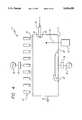
- FIG. 1is a schematic side view illustrating a first embodiment of the plasma generator of the present invention for initiating a plasma through capacitive coupling;
- FIG. 2is a schematic side view of alternative embodiments of the plasma generator of the present invention for initiating a plasma through capacitive coupling;
- FIG. 3is a schematic side view of an embodiment of the plasma generator of the present invention for initiating a plasma through ionization of some of a process gas
- FIG. 4is a schematic side view of further embodiments of the plasma generator of the present invention for initiating a plasma through ionization of some of a process gas.
- the apparatus 10includes a vacuum chamber 12 having a gas inlet line 14 and a vacuum exhaust outlet line 16.
- the vacuum chamber 12is preferably composed of a nonconductive material, such as an anodized metal grounded by an appropriately configured ground line 18.
- a target pedestal 20Disposed within the vacuum chamber 12 is a target pedestal 20 for supporting one or more semiconductor wafers 22.
- One surface of the vacuum chamber 12 opposite to and generally parallel with the pedestal 20defines an aperture within which a dielectric window 24 is disposed.
- This dielectric window 24may be composed of quartz or some other suitable dielectric material such as various nonconductive ceramics known in the electromagnetic arts.
- a generally planar coil 26is further disposed outside the vacuum chamber 12 adjacent the dielectric window 24. This coil 26 provides the primary source of power to sustain by inductive coupling a plasma within the vacuum chamber 12.
- the dielectric window 24provides an atmospheric seal with the vacuum chamber 12 that is generally transmissive to an electromagnetic field generated by the coil 26.
- the coil 26is generally planar, with deviations in flatness of preferably, but not necessarily, less than one to two-tenths of the diameter of the coil.
- the coil 26may further form a spiral configuration or, alternatively, a series of interconnected concentric rings.
- the diameter of the coil 26is typically dependent upon the size of the plasma desired.
- a coil 26, intended for sustaining a plasma of sufficient size to treat a single semiconductor waferhas a diameter of thirteen to eighteen centimeters with five to eight spiral turns or concentric rings provided to produce a relatively uniform plasma within the vacuum chamber 12 that extends essentially across the entire diameter of the coil 26.
- the coil 26is composed of a highly conductive metal, such as copper, having a sufficient cross-sectional diameter to accommodate currents of up to approximately thirty amps.
- RF power source 28is provided to the coil 26 by a radio frequency (RF) power source 28.
- the power source 28may be inductively coupled to the coil 26 by a matching circuit 30, or by some other appropriate circuitry known in the electrical arts.
- this matched circuitincludes a primary coil coupled to the RF power source 28 and a secondary loop coupled to the inner and outer ends of the coil 26 in series with a variable capacitor.
- the primary coil and secondary loopmay be orientable with respect to one another to allow for circuit loading at a desired operating frequency of the power source 28.
- the variable capacitor in series with the secondary loopfurther permits adjustment of the resonant frequency of the circuit to match the frequency output of the power source 28.
- the RF power source 28preferably, but not necessarily, has a power output of about 500 watts in the megahertz frequency range with an RMS voltage output of about 70,000 volts.
- a plasma sustained by the apparatus 10 illustrated in FIG. 1 and discussed abovewill have a velocity vector oriented generally parallel to the surface of the semiconductor wafer 22 within the vacuum chamber 12.
- the pedestal 20may be coupled to a separate RF power source 32 through an additional matching circuit 34.
- the vacuum chamber 12is pumped to a desired operating pressure with a process gas being introduced into the vacuum chamber 12 through the inlet 14.
- a plasmais then initiated within the vacuum chamber 12.
- Inductive coupling between the coil 26 and the process gascan sustain the plasma once it is initiated.
- Plasma initiationtypically cannot be achieved by inductive coupling between the coil 26 and the process gas at pressures in the low millitorr range.
- the inventorshave determined, however, that damage may be imparted to semiconductor wafers intended for plasma treatment at pressures in the low millitorr range if a plasma is first initiated at higher pressures and then reduced to a desired operating pressure in the low millitorr range, for example, two to three millitorr.
- the present inventionprovides an apparatus for exposing a semiconductor wafer to a low pressure plasma in the two to three millitorr range for a period of thirty seconds or less.
- the present inventionprovides several alternative mechanisms for igniting a plasma within the vacuum chamber 12 at pressures in the low millitorr range, and well below those at which the coil 26 alone can ignite a plasma.
- a secondary electrode 40is included within the vacuum chamber 12 and coupled by a matched circuit 42 to a second radio frequency power source 44.
- This secondary electrode 40is intended to increase the energy of free electrons that are already present in the process gas primarily by capacitive coupling.
- the inventorshave determined that the extremely high resistive character of the dielectric window 24, and the concomitant voltage drop across this window, usually prevents sufficient capacitive coupling between the coil 26 and a process gas disposed within the vacuum chamber 12.
- sufficient capacitive couplingmay be achieved by introduction of suitable RF energy from the second radio frequency power source 44 to achieve plasma ignition at pressures in the low seven millitorr range, and in fact, within desired operating ranges of two to three millitorr.
- capacitive coupling between the secondary electrode 40may be enhanced by use of the separate RF power supply 32 coupled to the semiconductor wafer support pedestal 20 through the matching circuit 34.
- both the RF power source 44, coupled to the secondary electrode 40, and the separate RF power source 32 coupled to the wafer pedestal 20are activated.
- the relative phase of the RF outputs from these two RF power sourcesis initially set approximately 180° from one another. This phase separation can be selected to optimally enhance the capacitive coupling between the secondary electrode 40 and the pedestal 20, thus substantially increasing the energy transferred to free electrons already present in the process gas.
- the RF power source 44 coupled to the secondary electrode 40may be deactivated and the phase of the separate RF power supply 32 coupled to the wafer pedestal 20 may be altered to optimize coupling between the pedestal 20 and the generally planar coil 26 disposed exterior to the vacuum chamber.
- a single RF power supply 60may be coupled to both the pedestal 20 and the secondary electrode 40 through a power splitter 62.
- a signal delay 64may also beneficially be included between the power splitter 62 and either the pedestal 20 or the secondary electrode 40.
- the power splitter 64is variable so that the relative ratios of RF power provided to the pedestal 20 and the secondary electrode 40 may be varied.
- a desired operating pressure of the processing gasis obtained in the vacuum chamber 12 and the generally planar coil 26 disposed exterior to the vacuum chamber 12 is energized.
- RF poweris then provided to the secondary coil 40 and the pedestal 20 to ignite a plasma within the process gas.
- the signal delayis then preferably used to vary the relative phase of the RF power being applied to the secondary electrode 40 and the pedestal 20 so as to maximize capacitive coupling between the two elements.
- RF power flow to the secondary electrode 40may be terminated.
- the output of the RF power supply 60may then be configured to optimize operation in cooperation with the generally planar coil 26.
- FIG. 3An alternative embodiment of the present invention, illustrated in FIG. 3, employs a different approach to plasma ignition at pressures insufficient for plasma ignition by the coil 26 alone.
- a plasmais first formed in the process gas by another ionizing mechanism. Once the process gas has been ionized, there is sufficient plasma species present to support inductive coupling with the primary coil 26.
- the process gasis initially ionized by introduction of an ionizing light beam from a source 48 exterior to the vacuum chamber 12.
- the vacuum chamber 12is further provided with a window 50 that is transmissive to the ultraviolet portion of the electromagnetic spectrum.
- further ionization of the process gas within the vacuum chamber 12may be achieved by employing an ionizing light source.
- plasma ignitionis achieved by partially ionizing a portion of the process gas within the vacuum chamber 12 through some mechanism independent of the generally planar coil 26 that is used to sustain the plasma through inductive coupling.
- this partial ionization of the process gasmay be achieved by a tesla coil 52 having a high power output rod 54 disposed within the vacuum chamber 12.
- a high voltage at the end of the output rod 54 caused by operation of the tesla coil 52would cause arcing in the process gas-between the electrode 54 and the conductive walls of the vacuum chamber 12 grounded by line 18.
- a pair of electrodes having an extremely high potential between themcould be employed by way of example, as further illustrated in FIG. 4, a spark plug 58 including electrodes 60 and 62 could be coupled to an appropriate high voltage source (not shown) to achieve a spark across the electrodes 60 and 62 by conventional means.
- a further aspect of the inventionconcerns varying the character of the reactive gas species in a plasma for processing a semiconductor wafer without also varying the plasma conditions directly.
- Conventional semiconductor processing techniques involving exposure of the semiconductor wafer to a process plasmanormally require variations in the plasma conditions to induce changes in the character of the reactive gas species.
- the absolute quantity of reactive gas species present in the plasma, or the ratio of neutral species to ionize species in the plasmaare both normally dependent upon several factors, including (but not limited to) the composition of the input gas mixture, the plasma pressure and the magnitude of the radio frequency or magnetic power input to the plasma. Each of these factors, however, are also known to adversely effect the character of the semiconductor processing.
- Various semiconductor processing characteristicssuch as for example, the straightness of the plasma etched into the semiconductor wafer, the selectivity of the plasma gases to the materials distributed over portions of the semiconductor wafer, and the cleanliness of a semiconductor wafer etch are normally dependent on the absolute molar quantity of the reactive species in the plasma gas mixture and the ratios of the active components of the plasma.
- alterations in the absolute quantity of reactive species or in the ratio of the active plasma components to achieve a desired semiconductor wafer processing characteristicnormally can only be achieved through conventional processes by alterations in the plasma condition (such as pressure or power input) that are also known to influence the desired semiconductor wafer processing characteristic. Changes in the character of the plasma intended to improve the semiconductor wafer process are thus achieved by conventional processes only through methods that are also known to cause other adverse effects in the plasma process.
- variations in the composition of reactive species, as well as variations in the absolute quantity of reactive species in the plasma gas mixture and the ratios of active components in the plasmamay be achieved by methods and apparatus other than direct variations of plasma pressure, changes in the composition of the plasma input gas, or direct alteration of the radio frequency or magnetic power input into the plasma. More particularly, in accordance with this aspect of the invention optical energy of a selected wavelength or frequency is introduced into the plasma to achieve variations in either or all of the absolute molar quantity of reactive species, composition of reactive species, and the ratios of neutral to ionized species.
- This aspect of the inventiontakes advantage of differences in quantum mechanical energy absorption selection rules for the absorption of optical energy compared to the absorption of RF energy so as to disassociate gas molecules of the type that are normally employed in semiconductor plasma processing.
- optical energy in the two to five micron range of the infrared spectrumare known to be characteristic of stretching the vibrations between single and triple molecular bonds.
- optical energy in the eleven to sixteen micron range of the infrared spectrumare known to induce strong aryl, out-of-plane deformation vibrations in C--H bonds. This introduction of a sufficient magnitude of optical energy in these and higher energy ranges are known to break these bonds. It is believed application of the well known Beer-Lambert Law of Absorption may be employed to control the result in concentration of components obtained by breaking these bonds.
- the introduction of optical energy of appropriate wavelength or frequency in a process plasma created or sustained by otherwise conventional methodologiesaccommodates the formation of plasma gas mixtures with chemically reactive compounds that can be selected and quantitatively controlled by the amount of both RF and optical energy that is added to the plasma.
- various desired characteristics of the reactive species, as well as the precise composition of the reactive species,may all be altered without resorting to gross variations in the characteristics of the plasma itself.
- the concentration of reactive speciesmay be increased by comparing absorption spectra of the input gas mixture with absorption spectra of the known reactive species created by the plasma process.
- Optical energy in the frequency range of absorption bands that are present in the input gas mixture but absent from the reactive speciesare expected to be the desired frequencies for creating an additional quantity of a known reactive species.
- Introduction of optical energy in these disparate absorption bands into the plasmashould therefore create additional quantities of the reactive species within the plasma.
- entirely new classes of reactive speciesmay be created by introducing optical energy of differing frequencies into the plasma.
- optical energy in the two to five micron rangemay be employed to disassociate most forms of carbon-based gas mixtures, such as CF 4 or C 2 F 6 , employed in plasma processing of a semiconductor wafer, resulting in the formation of entirely new reactive gas species.
- the optical energy source 48need not necessarily generate optical energy in the ultraviolet portion of the spectrum and, similarly, the window 50 need not necessarily be transparent in the ultraviolet.
- the optical source 48preferably generates optical radiation in a portion of the spectrum known to be responsible for inducing the desired characteristics in the reactive species. The optical source 48 thus could generate optical radiation in the visible, or even in the infrared portion, of the optical spectrum, depending on the changes to the reactive species that are desired.
- the optical radiation source 48may be of any source generating sufficient radiation at a desired frequency or wavelength.
- the source 48may be a laser, or may be one or a variety of ultraviolet, visible or infrared broad band sources that is further provided with an appropriate filter so as to limit the frequency of optical radiation directed into the process plasma to a desired spectral band.
- beam steering apparatus 70may also be included to alter the position of an optical radiation beam directed towards the semiconductor wafer processing plasma.
- Beam steering apparatuscapable of altering the location of a beam with respect to two orthogonal axes are well known in the optical arts and are available from a variety of vendors including Newport Research Optical in Newport Beach, Calif.
- the beam steering apparatus 70may further be provided with focusing elements (not shown) so as to varying the energy density of the optical radiation along the axis of propagation. Further use of beam focusing elements permits control of the position and energy density of the optical radiation beam with respect to three mutually perpendicular axes.
- the present inventionprovides a means of operating an inductively-coupled plasma generating device capable of creating a highly uniform plasma across a wide range of operating pressures.
- the present inventionavoids disadvantages found to occur in conventional practices of initiating a plasma by raising the pressure of a process gas to a pressure sufficient to support plasma ignition and then gradually lowering the pressure to a desired operating range.
- the optical radiation source illustrated in FIG. 3could, in any of the embodiments discussed above, be alternatively disposed within the vacuum chamber 12, or located upstream of the vacuum chamber 12 remote from the semiconductor wafer. In either instance the need for the optical window 50 would be eliminated. Accordingly, the scope of the present invention should not be limited by the particular embodiments discussed above, but should be defined only by the claims set forth below and equivalence thereof.
Landscapes
- Chemical & Material Sciences (AREA)
- Physics & Mathematics (AREA)
- Engineering & Computer Science (AREA)
- Plasma & Fusion (AREA)
- Analytical Chemistry (AREA)
- General Chemical & Material Sciences (AREA)
- Electromagnetism (AREA)
- Toxicology (AREA)
- Health & Medical Sciences (AREA)
- Chemical Kinetics & Catalysis (AREA)
- Materials Engineering (AREA)
- Mechanical Engineering (AREA)
- Metallurgy (AREA)
- Organic Chemistry (AREA)
- Plasma Technology (AREA)
- Drying Of Semiconductors (AREA)
Abstract
Description
Claims (13)
Priority Applications (1)
| Application Number | Priority Date | Filing Date | Title |
|---|---|---|---|
| US08/485,517US5696428A (en) | 1995-06-07 | 1995-06-07 | Apparatus and method using optical energy for specifying and quantitatively controlling chemically-reactive components of semiconductor processing plasma etching gas |
Applications Claiming Priority (1)
| Application Number | Priority Date | Filing Date | Title |
|---|---|---|---|
| US08/485,517US5696428A (en) | 1995-06-07 | 1995-06-07 | Apparatus and method using optical energy for specifying and quantitatively controlling chemically-reactive components of semiconductor processing plasma etching gas |
Publications (1)
| Publication Number | Publication Date |
|---|---|
| US5696428Atrue US5696428A (en) | 1997-12-09 |
Family
ID=23928471
Family Applications (1)
| Application Number | Title | Priority Date | Filing Date |
|---|---|---|---|
| US08/485,517Expired - LifetimeUS5696428A (en) | 1995-06-07 | 1995-06-07 | Apparatus and method using optical energy for specifying and quantitatively controlling chemically-reactive components of semiconductor processing plasma etching gas |
Country Status (1)
| Country | Link |
|---|---|
| US (1) | US5696428A (en) |
Cited By (17)
| Publication number | Priority date | Publication date | Assignee | Title |
|---|---|---|---|---|
| US5964949A (en)* | 1996-03-06 | 1999-10-12 | Mattson Technology, Inc. | ICP reactor having a conically-shaped plasma-generating section |
| US5983828A (en)* | 1995-10-13 | 1999-11-16 | Mattson Technology, Inc. | Apparatus and method for pulsed plasma processing of a semiconductor substrate |
| US6312555B1 (en) | 1996-09-11 | 2001-11-06 | Ctp, Inc. | Thin film electrostatic shield for inductive plasma processing |
| US6379576B2 (en) | 1997-11-17 | 2002-04-30 | Mattson Technology, Inc. | Systems and methods for variable mode plasma enhanced processing of semiconductor wafers |
| US6395641B2 (en) | 1995-10-13 | 2002-05-28 | Mattson Techonolgy, Inc. | Apparatus and method for pulsed plasma processing of a semiconductor substrate |
| US6551447B1 (en) | 1994-11-15 | 2003-04-22 | Mattson Technology, Inc. | Inductive plasma reactor |
| US6566272B2 (en) | 1999-07-23 | 2003-05-20 | Applied Materials Inc. | Method for providing pulsed plasma during a portion of a semiconductor wafer process |
| US6650678B1 (en)* | 1999-02-26 | 2003-11-18 | Canon Kabushiki Kaisha | Laser oscillating apparatus |
| US20040085023A1 (en)* | 2002-11-04 | 2004-05-06 | Roman Chistyakov | Methods and apparatus for generating high-density plasma |
| US6794301B2 (en) | 1995-10-13 | 2004-09-21 | Mattson Technology, Inc. | Pulsed plasma processing of semiconductor substrates |
| US20040244691A1 (en)* | 2003-04-01 | 2004-12-09 | Rene George | Slotted electrostatic shield modification for improved etch and CVD process uniformity |
| US20100186670A1 (en)* | 2007-07-12 | 2010-07-29 | Imagineering, Inc. | Plasma formation region control apparatus and plasma processing apparatus |
| US20110234019A1 (en)* | 2007-08-17 | 2011-09-29 | Tmms Co., Ltd. | Method and device for transporting, distributing and managing electrical energy by remote longitudinal coupling in near field between electric dipoles |
| US20140227861A1 (en)* | 2013-02-08 | 2014-08-14 | Taiwan Semiconductor Manufacturing Co., Ltd. | Bottom-Up PEALD Process |
| US20160121418A1 (en)* | 2012-01-25 | 2016-05-05 | Gordon Hanka | Welder Powered Arc Starter |
| WO2021030342A1 (en)* | 2019-08-12 | 2021-02-18 | Mattson Technology, Inc. | Enhanced ignition in inductively coupled plasmas for workpiece processing |
| US20220115211A1 (en)* | 2019-05-09 | 2022-04-14 | Spp Technologies Co., Ltd. | Method of igniting plasma and plasma generating system |
Citations (19)
| Publication number | Priority date | Publication date | Assignee | Title |
|---|---|---|---|---|
| US4557819A (en)* | 1984-07-20 | 1985-12-10 | Varian Associates, Inc. | System for igniting and controlling a wafer processing plasma |
| US4664938A (en)* | 1985-05-06 | 1987-05-12 | Phillips Petroleum Company | Method for deposition of silicon |
| US4804431A (en)* | 1987-11-03 | 1989-02-14 | Aaron Ribner | Microwave plasma etching machine and method of etching |
| US4863559A (en)* | 1988-02-22 | 1989-09-05 | Texas Instruments Incorporated | Method for forming local interconnects using chlorine bearing agents |
| US4877642A (en)* | 1986-07-05 | 1989-10-31 | U.S. Philips Corp. | Method of manufacturing electrically conductive molded bodies by plasma-activated chemical deposition from the gaseous phase |
| US4891118A (en)* | 1987-11-25 | 1990-01-02 | Fuji Electric Co., Ltd. | Plasma processing apparatus |
| US4946537A (en)* | 1988-07-12 | 1990-08-07 | Tokyo Ohka Kogyo Co., Ltd. | Plasma reactor |
| US4948458A (en)* | 1989-08-14 | 1990-08-14 | Lam Research Corporation | Method and apparatus for producing magnetically-coupled planar plasma |
| US4957590A (en)* | 1988-02-22 | 1990-09-18 | Texas Instruments Incorporated | Method for forming local interconnects using selective anisotropy |
| US5006760A (en)* | 1987-01-09 | 1991-04-09 | Motorola, Inc. | Capacitive feed for plasma reactor |
| US5032221A (en)* | 1990-05-07 | 1991-07-16 | Eastman Kodak Company | Etching indium tin oxide |
| US5078823A (en)* | 1989-05-18 | 1992-01-07 | Defitech S.A. | Plasma reactor |
| US5171401A (en)* | 1990-06-04 | 1992-12-15 | Eastman Kodak Company | Plasma etching indium tin oxide |
| US5183775A (en)* | 1990-01-23 | 1993-02-02 | Applied Materials, Inc. | Method for forming capacitor in trench of semiconductor wafer by implantation of trench surfaces with oxygen |
| US5272417A (en)* | 1989-05-12 | 1993-12-21 | Tadahiro Ohmi | Device for plasma process |
| US5277751A (en)* | 1992-06-18 | 1994-01-11 | Ogle John S | Method and apparatus for producing low pressure planar plasma using a coil with its axis parallel to the surface of a coupling window |
| US5310452A (en)* | 1989-04-27 | 1994-05-10 | Fujitsu Limited | Plasma process apparatus and plasma processing method |
| US5346578A (en)* | 1992-11-04 | 1994-09-13 | Novellus Systems, Inc. | Induction plasma source |
| US5468296A (en)* | 1993-12-17 | 1995-11-21 | Lsi Logic Corporation | Apparatus for igniting low pressure inductively coupled plasma |
- 1995
- 1995-06-07USUS08/485,517patent/US5696428A/ennot_activeExpired - Lifetime
Patent Citations (20)
| Publication number | Priority date | Publication date | Assignee | Title |
|---|---|---|---|---|
| US4557819A (en)* | 1984-07-20 | 1985-12-10 | Varian Associates, Inc. | System for igniting and controlling a wafer processing plasma |
| US4664938A (en)* | 1985-05-06 | 1987-05-12 | Phillips Petroleum Company | Method for deposition of silicon |
| US4877642A (en)* | 1986-07-05 | 1989-10-31 | U.S. Philips Corp. | Method of manufacturing electrically conductive molded bodies by plasma-activated chemical deposition from the gaseous phase |
| US5006760A (en)* | 1987-01-09 | 1991-04-09 | Motorola, Inc. | Capacitive feed for plasma reactor |
| US4804431A (en)* | 1987-11-03 | 1989-02-14 | Aaron Ribner | Microwave plasma etching machine and method of etching |
| US4891118A (en)* | 1987-11-25 | 1990-01-02 | Fuji Electric Co., Ltd. | Plasma processing apparatus |
| US4863559A (en)* | 1988-02-22 | 1989-09-05 | Texas Instruments Incorporated | Method for forming local interconnects using chlorine bearing agents |
| US4957590A (en)* | 1988-02-22 | 1990-09-18 | Texas Instruments Incorporated | Method for forming local interconnects using selective anisotropy |
| US4863559B1 (en)* | 1988-02-22 | 2000-11-21 | Texas Instruments Inc | Method for forming local interconnects using chlorine bearing agents |
| US4946537A (en)* | 1988-07-12 | 1990-08-07 | Tokyo Ohka Kogyo Co., Ltd. | Plasma reactor |
| US5310452A (en)* | 1989-04-27 | 1994-05-10 | Fujitsu Limited | Plasma process apparatus and plasma processing method |
| US5272417A (en)* | 1989-05-12 | 1993-12-21 | Tadahiro Ohmi | Device for plasma process |
| US5078823A (en)* | 1989-05-18 | 1992-01-07 | Defitech S.A. | Plasma reactor |
| US4948458A (en)* | 1989-08-14 | 1990-08-14 | Lam Research Corporation | Method and apparatus for producing magnetically-coupled planar plasma |
| US5183775A (en)* | 1990-01-23 | 1993-02-02 | Applied Materials, Inc. | Method for forming capacitor in trench of semiconductor wafer by implantation of trench surfaces with oxygen |
| US5032221A (en)* | 1990-05-07 | 1991-07-16 | Eastman Kodak Company | Etching indium tin oxide |
| US5171401A (en)* | 1990-06-04 | 1992-12-15 | Eastman Kodak Company | Plasma etching indium tin oxide |
| US5277751A (en)* | 1992-06-18 | 1994-01-11 | Ogle John S | Method and apparatus for producing low pressure planar plasma using a coil with its axis parallel to the surface of a coupling window |
| US5346578A (en)* | 1992-11-04 | 1994-09-13 | Novellus Systems, Inc. | Induction plasma source |
| US5468296A (en)* | 1993-12-17 | 1995-11-21 | Lsi Logic Corporation | Apparatus for igniting low pressure inductively coupled plasma |
Non-Patent Citations (1)
| Title |
|---|
| Nyaiesh et al., U.S. Statutory Invention Registration H566, Jan. 3, 1989.* |
Cited By (33)
| Publication number | Priority date | Publication date | Assignee | Title |
|---|---|---|---|---|
| US6551447B1 (en) | 1994-11-15 | 2003-04-22 | Mattson Technology, Inc. | Inductive plasma reactor |
| US5983828A (en)* | 1995-10-13 | 1999-11-16 | Mattson Technology, Inc. | Apparatus and method for pulsed plasma processing of a semiconductor substrate |
| US6395641B2 (en) | 1995-10-13 | 2002-05-28 | Mattson Techonolgy, Inc. | Apparatus and method for pulsed plasma processing of a semiconductor substrate |
| US6794301B2 (en) | 1995-10-13 | 2004-09-21 | Mattson Technology, Inc. | Pulsed plasma processing of semiconductor substrates |
| US5964949A (en)* | 1996-03-06 | 1999-10-12 | Mattson Technology, Inc. | ICP reactor having a conically-shaped plasma-generating section |
| US6312555B1 (en) | 1996-09-11 | 2001-11-06 | Ctp, Inc. | Thin film electrostatic shield for inductive plasma processing |
| US6379576B2 (en) | 1997-11-17 | 2002-04-30 | Mattson Technology, Inc. | Systems and methods for variable mode plasma enhanced processing of semiconductor wafers |
| US6536449B1 (en) | 1997-11-17 | 2003-03-25 | Mattson Technology Inc. | Downstream surface cleaning process |
| US6650678B1 (en)* | 1999-02-26 | 2003-11-18 | Canon Kabushiki Kaisha | Laser oscillating apparatus |
| US6566272B2 (en) | 1999-07-23 | 2003-05-20 | Applied Materials Inc. | Method for providing pulsed plasma during a portion of a semiconductor wafer process |
| US20040085023A1 (en)* | 2002-11-04 | 2004-05-06 | Roman Chistyakov | Methods and apparatus for generating high-density plasma |
| WO2004042774A1 (en)* | 2002-11-04 | 2004-05-21 | Zond, Inc | Methods and apparatus for generating high-density plasma |
| US7604716B2 (en) | 2002-11-04 | 2009-10-20 | Zond, Inc. | Methods and apparatus for generating high-density plasma |
| US20050006220A1 (en)* | 2002-11-04 | 2005-01-13 | Roman Chistyakov | Methods and apparatus for generating high-density plasma |
| US6853142B2 (en) | 2002-11-04 | 2005-02-08 | Zond, Inc. | Methods and apparatus for generating high-density plasma |
| US7232767B2 (en) | 2003-04-01 | 2007-06-19 | Mattson Technology, Inc. | Slotted electrostatic shield modification for improved etch and CVD process uniformity |
| US20070113979A1 (en)* | 2003-04-01 | 2007-05-24 | Rene George | Slotted Electrostatic Shield Modification for Improved Etch and CVD Process Uniformity |
| US20040244691A1 (en)* | 2003-04-01 | 2004-12-09 | Rene George | Slotted electrostatic shield modification for improved etch and CVD process uniformity |
| US8413604B2 (en) | 2003-04-01 | 2013-04-09 | Mattson Technology, Inc. | Slotted electrostatic shield modification for improved etch and CVD process uniformity |
| US20100186670A1 (en)* | 2007-07-12 | 2010-07-29 | Imagineering, Inc. | Plasma formation region control apparatus and plasma processing apparatus |
| US8552650B2 (en)* | 2007-07-12 | 2013-10-08 | Imagineering, Inc. | Plasma formation region control apparatus and plasma processing apparatus |
| US20110234019A1 (en)* | 2007-08-17 | 2011-09-29 | Tmms Co., Ltd. | Method and device for transporting, distributing and managing electrical energy by remote longitudinal coupling in near field between electric dipoles |
| US8847432B2 (en)* | 2007-08-17 | 2014-09-30 | Murata Manufacturing Co., Ltd. | Method and device for transporting, distributing and managing electrical energy by remote longitudinal coupling in near field between electric dipoles |
| US20160121418A1 (en)* | 2012-01-25 | 2016-05-05 | Gordon Hanka | Welder Powered Arc Starter |
| US9184045B2 (en)* | 2013-02-08 | 2015-11-10 | Taiwan Semiconductor Manufacturing Co., Ltd. | Bottom-up PEALD process |
| US20140227861A1 (en)* | 2013-02-08 | 2014-08-14 | Taiwan Semiconductor Manufacturing Co., Ltd. | Bottom-Up PEALD Process |
| US10121653B2 (en) | 2013-02-08 | 2018-11-06 | Taiwan Semiconductor Manufacturing Co., Ltd. | Bottom-up PEALD proces |
| US20220115211A1 (en)* | 2019-05-09 | 2022-04-14 | Spp Technologies Co., Ltd. | Method of igniting plasma and plasma generating system |
| TWI868128B (en)* | 2019-05-09 | 2025-01-01 | 日商Spp科技股份有限公司 | Plasma ignition method and plasma generating device |
| WO2021030342A1 (en)* | 2019-08-12 | 2021-02-18 | Mattson Technology, Inc. | Enhanced ignition in inductively coupled plasmas for workpiece processing |
| US11348784B2 (en) | 2019-08-12 | 2022-05-31 | Beijing E-Town Semiconductor Technology Co., Ltd | Enhanced ignition in inductively coupled plasmas for workpiece processing |
| US11848204B2 (en) | 2019-08-12 | 2023-12-19 | Beijing E-Town Semiconductor Technology Co., Ltd | Enhanced ignition in inductively coupled plasmas for workpiece processing |
| US12347677B2 (en) | 2019-08-12 | 2025-07-01 | Beijing E-town Semiconductor Technology Co., Ltd. | Enhanced ignition in inductively coupled plasmas for workpiece processing |
Similar Documents
| Publication | Publication Date | Title |
|---|---|---|
| US6062163A (en) | Plasma initiating assembly | |
| US5696428A (en) | Apparatus and method using optical energy for specifying and quantitatively controlling chemically-reactive components of semiconductor processing plasma etching gas | |
| KR100291152B1 (en) | Plasma generating apparatus | |
| JP3739137B2 (en) | Plasma generator and surface treatment apparatus using the plasma generator | |
| US9966239B2 (en) | Non-ambipolar plasma enhanced DC/VHF phasor | |
| US4948458A (en) | Method and apparatus for producing magnetically-coupled planar plasma | |
| KR102812235B1 (en) | Improved ignition of inductively coupled plasma for workpiece treatment | |
| Conrads et al. | Plasma generation and plasma sources | |
| KR930005945B1 (en) | Plasma processing apparatus | |
| JP3158236B2 (en) | Apparatus and method for igniting a plasma in a process module | |
| EP0710056B1 (en) | Radio-frequency plasma source | |
| US20080156631A1 (en) | Methods of Producing Plasma in a Container | |
| US5489362A (en) | Method for generating excited neutral particles for etching and deposition processes in semiconductor technology with a plasma discharge fed by microwave energy | |
| JP2006505128A (en) | Plasma treatment magnetically enhanced by high power pulses | |
| KR20020031344A (en) | Plasma processor with coil responsive to variable amplitude rf envelope | |
| CN100417308C (en) | Apparatus and method for forming plasma | |
| CN101366101B (en) | Method and apparatus for igniting a low-pressure plasma | |
| JPH09115694A (en) | Plasma treatment device | |
| US10588212B1 (en) | Plasma initiation in an inductive RF coupling mode | |
| JP2760845B2 (en) | Plasma processing apparatus and method | |
| Johnson | Electrostaticallyshielded inductively-coupled RF plasma source | |
| US20040140778A1 (en) | Plasma generation system | |
| JPH0635663B2 (en) | Surface treatment method and apparatus | |
| JPH09161993A (en) | Plasma processing apparatus and method having multi-stage coil using double coil | |
| JPH05251390A (en) | Plasma device |
Legal Events
| Date | Code | Title | Description |
|---|---|---|---|
| AS | Assignment | Owner name:LSI LOGIC CORPORATION, CALIFORNIA Free format text:ASSIGNMENT OF ASSIGNORS INTEREST;ASSIGNOR:PASCH, NICHOLAS F.;REEL/FRAME:007753/0591 Effective date:19951107 | |
| STCF | Information on status: patent grant | Free format text:PATENTED CASE | |
| FPAY | Fee payment | Year of fee payment:4 | |
| FPAY | Fee payment | Year of fee payment:8 | |
| FEPP | Fee payment procedure | Free format text:PAYER NUMBER DE-ASSIGNED (ORIGINAL EVENT CODE: RMPN); ENTITY STATUS OF PATENT OWNER: LARGE ENTITY Free format text:PAYOR NUMBER ASSIGNED (ORIGINAL EVENT CODE: ASPN); ENTITY STATUS OF PATENT OWNER: LARGE ENTITY | |
| FPAY | Fee payment | Year of fee payment:12 | |
| AS | Assignment | Owner name:DEUTSCHE BANK AG NEW YORK BRANCH, AS COLLATERAL AG Free format text:PATENT SECURITY AGREEMENT;ASSIGNORS:LSI CORPORATION;AGERE SYSTEMS LLC;REEL/FRAME:032856/0031 Effective date:20140506 | |
| AS | Assignment | Owner name:LSI CORPORATION, CALIFORNIA Free format text:CHANGE OF NAME;ASSIGNOR:LSI LOGIC CORPORATION;REEL/FRAME:033102/0270 Effective date:20070406 | |
| AS | Assignment | Owner name:AVAGO TECHNOLOGIES GENERAL IP (SINGAPORE) PTE. LTD Free format text:ASSIGNMENT OF ASSIGNORS INTEREST;ASSIGNOR:LSI CORPORATION;REEL/FRAME:035390/0388 Effective date:20140814 | |
| AS | Assignment | Owner name:AGERE SYSTEMS LLC, PENNSYLVANIA Free format text:TERMINATION AND RELEASE OF SECURITY INTEREST IN PATENT RIGHTS (RELEASES RF 032856-0031);ASSIGNOR:DEUTSCHE BANK AG NEW YORK BRANCH, AS COLLATERAL AGENT;REEL/FRAME:037684/0039 Effective date:20160201 Owner name:LSI CORPORATION, CALIFORNIA Free format text:TERMINATION AND RELEASE OF SECURITY INTEREST IN PATENT RIGHTS (RELEASES RF 032856-0031);ASSIGNOR:DEUTSCHE BANK AG NEW YORK BRANCH, AS COLLATERAL AGENT;REEL/FRAME:037684/0039 Effective date:20160201 | |
| AS | Assignment | Owner name:BELL SEMICONDUCTOR, LLC, ILLINOIS Free format text:ASSIGNMENT OF ASSIGNORS INTEREST;ASSIGNORS:AVAGO TECHNOLOGIES GENERAL IP (SINGAPORE) PTE. LTD.;BROADCOM CORPORATION;REEL/FRAME:044886/0608 Effective date:20171208 | |
| AS | Assignment | Owner name:CORTLAND CAPITAL MARKET SERVICES LLC, AS COLLATERA Free format text:SECURITY INTEREST;ASSIGNORS:HILCO PATENT ACQUISITION 56, LLC;BELL SEMICONDUCTOR, LLC;BELL NORTHERN RESEARCH, LLC;REEL/FRAME:045216/0020 Effective date:20180124 | |
| AS | Assignment | Owner name:BELL NORTHERN RESEARCH, LLC, ILLINOIS Free format text:RELEASE BY SECURED PARTY;ASSIGNOR:CORTLAND CAPITAL MARKET SERVICES LLC;REEL/FRAME:059720/0719 Effective date:20220401 Owner name:BELL SEMICONDUCTOR, LLC, ILLINOIS Free format text:RELEASE BY SECURED PARTY;ASSIGNOR:CORTLAND CAPITAL MARKET SERVICES LLC;REEL/FRAME:059720/0719 Effective date:20220401 Owner name:HILCO PATENT ACQUISITION 56, LLC, ILLINOIS Free format text:RELEASE BY SECURED PARTY;ASSIGNOR:CORTLAND CAPITAL MARKET SERVICES LLC;REEL/FRAME:059720/0719 Effective date:20220401 |