US5694063A - High speed IDDQ monitor circuit - Google Patents
High speed IDDQ monitor circuitDownload PDFInfo
- Publication number
- US5694063A US5694063AUS08/721,973US72197396AUS5694063AUS 5694063 AUS5694063 AUS 5694063AUS 72197396 AUS72197396 AUS 72197396AUS 5694063 AUS5694063 AUS 5694063A
- Authority
- US
- United States
- Prior art keywords
- node
- voltage
- ddq
- switch
- power supply
- Prior art date
- Legal status (The legal status is an assumption and is not a legal conclusion. Google has not performed a legal analysis and makes no representation as to the accuracy of the status listed.)
- Expired - Lifetime
Links
Images


Classifications
- G—PHYSICS
- G01—MEASURING; TESTING
- G01R—MEASURING ELECTRIC VARIABLES; MEASURING MAGNETIC VARIABLES
- G01R31/00—Arrangements for testing electric properties; Arrangements for locating electric faults; Arrangements for electrical testing characterised by what is being tested not provided for elsewhere
- G01R31/28—Testing of electronic circuits, e.g. by signal tracer
- G01R31/30—Marginal testing, e.g. by varying supply voltage
- G01R31/3004—Current or voltage test
- G01R31/3008—Quiescent current [IDDQ] test or leakage current test
- G—PHYSICS
- G01—MEASURING; TESTING
- G01R—MEASURING ELECTRIC VARIABLES; MEASURING MAGNETIC VARIABLES
- G01R31/00—Arrangements for testing electric properties; Arrangements for locating electric faults; Arrangements for electrical testing characterised by what is being tested not provided for elsewhere
- G01R31/28—Testing of electronic circuits, e.g. by signal tracer
- G01R31/317—Testing of digital circuits
- G01R31/3181—Functional testing
- G01R31/319—Tester hardware, i.e. output processing circuits
- G01R31/3193—Tester hardware, i.e. output processing circuits with comparison between actual response and known fault free response
Definitions
- the present inventionrelates to detection of defects in metal oxide semiconductor (MOS) circuits and more particularly to the detection of defects in complementary metal oxide semiconductor (CMOS) circuits by measuring the quiescent power supply current I DDQ of the device under test (DUT).
- MOSmetal oxide semiconductor
- CMOScomplementary metal oxide semiconductor
- VLSI circuitsare tested using automatic test equipment (“ATE") that typically test whether the VLSI circuit or device under test (“DUT”) is fully functional according to a "stuck-at fault” testing model.
- ATEautomatic test equipment
- DUTdevice under test
- Such functional testingrequires the application of a set of input "test vectors” to the DUT to determine if the DUT provides the expected output for each test vector.
- Test vectoris a combination of input signals that causes the logic of the DUT to change states. Whether the logic of the DUT changes states can be determined by monitoring the outputs of the DUT.
- defectsinclude (1) gate oxide shorts, (2) bridging defects, (3) punchthrough, (4) parasitic transistor leakage, (5) leaky p-n junctions, (6) open drain or source defects, (7) open gate defects, and (8) transmission gate opens. Devices having such defects may pass standard functional testing, but they will ultimately have a shorter life span than devices without such defects.
- testing the quiescent power supply current I DDQ of the DUTmay increase the rate of detection for the above-mentioned defects. It has also been discovered that testing the I DDQ of the DUT is useful for the detection of design and fabrication errors.
- the quiescent power supply current I DDQ of a CMOS DUTis theoretically equal to zero when the logic of the DUT is in any known state.
- FIG. 1Ashows a DUT 100 configured for testing by an ATE (not shown).
- the DUT 100includes a plurality of input conductors to which the ATE is coupled for providing input test vectors to the DUT 100.
- the DUT 100also includes a plurality of output conductors which are coupled to the ATE for providing output signals to the ATE in response to the input signals provided by the ATE.
- the ATEcan determine whether the logic of DUT 100 correctly changes states.
- the DUT 100may be, for example, a CMOS VLSI circuit comprising many thousands of CMOS inverters, the fundamental building block of CMOS circuits.
- CMOS inverteris shown as including an NMOS field effect transistor ("FET") Q1 and a PMOS FET Q2.
- FETfield effect transistor
- the gates of FET Q1 and FET Q2are coupled together for receiving the same input signal.
- the input signalmay be provided directly by an input conductor of the DUT 100 or by the output of another CMOS inverter.
- the drain of FET Q2is coupled to receive a power supply voltage V DD from a power supply, and the source of the FET Q2 is coupled to the drain of FET Q1.
- the source of FET Q1is coupled to system ground, VSS.
- the output of the CMOS inverteris taken from the node shared by the source of FET Q2 an the drain of FET Q1.
- the quiescent power supply current I DDQ of a CMOS inverteris ideally equal to zero because, theoretically, only one of the FETs Q1 and Q2 is switched on at any given time. Thus, no conduction path is provided between the power supply and ground. If the input signal is a logic low, FET Q2 is switched on and FET Q1 is switched off, which causes the output of the CMOS inverter to be tied to V DD , pulling the output up to a logic high level. Conversely, if the input signal is logic high, FET Q1 is switched on and FET Q2 is switched off, which causes the output of the CMOS inverter to be tied to VSS, pulling the output down to a logic low level. This behavior is shown in FIG. 1B. Curve 105 shows the input signal VIN, and curve 110 shows the output signal VOUT.
- the quiescent power supply current I DDQ of a typical CMOS inverteris some nominal, non-zero value. This is because neither of the FETs Q1 and Q2 are typically ever switched completely off, and a small conduction path is provided.
- a typical I DDQ value for a non-defective CMOSis less than 20 nA.
- Defective CMOS VLSI circuitscan exhibit elevated I DDQ levels in response to the appropriate test vectors.
- the defects listed abovetypically lead to conduction paths and therefore result in an elevation of the quiescent power supply current I DDQ that is greater than the I DDQ of a non-defective CMOS device.
- monitoring the I DDQ of a CMOS VLSI circuitcan result in the detection of defects that are unlikely to be detected using standard functional testing.
- FIG. 1Cshows the behavior of the power supply current I DD over time.
- the CMOS inverterBefore time t0, the CMOS inverter is in a known state, and the quiescent power supply current I DDQ is nominal value, as shown by arrow 115.
- the CMOS inverterchanges states, resulting in a current transient shown by arrow 120. This current transient is expected as both of the FETs Q1 and Q2 are conducting when switching between states.
- the power supply current I DDeventually settles to the nominal I DDQ . This is shown by arrow 125. If the CMOS inverter is defective, the I DDQ of the device is greater than the nominal value, as shown by arrow 130.
- FIG. 2shows a prior circuit for measuring the quiescent power supply current of a device under test.
- the circuit 200is coupled between a power supply 205 of the ATE and the DUT 100.
- the DUT 100is shown as including logic 225 coupled in parallel with the inherent capacitance of the DUT 100.
- the logic 225includes at least one CMOS inverter as described above.
- the circuit 200includes a switch 210 coupled between the power supply 205 and the DUT, capacitors C1 and C2, and buffer 220. During normal functional testing, the switch 210 is closed, providing a low impedance path between the power supply 205 and the DUT 100. This low impedance path allows the high transient currents that occur when the DUT changes states and provides the power supply voltage V DD to the DUT 100.
- the switch 210is shown as a FET having its gate controlled by a control signal of the ATE.
- the circuit 200measures the amount of quiescent power supply current I DDQ for the DUT 100 when the switch 210 is opened. To measure the quiescent power supply current I DDQ , the circuit 200 measures the time rate of change for the voltage at node 215.
- the input to the buffer 220provides a high input impedance value such that the only conduction path from the node 215 to system ground VSS is through the DUT 100.
- the output of the buffer 220which is equal to the value V DUT at node 215, is supplied to measurement circuitry in the ATE (not shown).
- the circuitoperates according to the well-known relationship between current, capacitance, and the time rate of change for voltage, namely: ##EQU1##
- I DDQquiescent power supply current
- the state of the logic 225is changed in response to an input test vector, giving rise to transient I DD current.
- the transientis allowed to subside, and the switch 210 is opened, decoupling the power supply 205 and the capacitor C1 from the node 215.
- the parallel capacitors of C2 and C DUTwere charged the power supply voltage V DD .
- the parallel capacitors C2 and C DUTbegin to discharge to ground via the DUT 100, giving rise to a current.
- the amount of current that is conducted via the DUT 100can be determined using equation 1.
- C totalwhich is the parallel capacitance of the capacitors C2 and C DUT
- C DUTmust be known.
- the requirement that C DUT must be knownis one disadvantage of this prior art I DDQ measurement technique.
- the measurement circuitry of the ATEsamples and holds the voltage at the output of the buffer 220. After a fixed amount of time equal to ⁇ t, the voltage at the output of the buffer 220 is sampled again. The difference between the two sampled voltages is determined to yield the change in voltage, ⁇ V. If the capacitance C total is known, the quiescent current I DDQ can be determined using the values ⁇ t, ⁇ V, and equation (1), above. The measured I DDQ value is then compared to an expected I DDQ value by the ATE, and the result of the comparison indicates whether the DUT passes or fails the I DDQ measurement test.
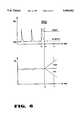
- FIG. 3shows the operating characteristics for the circuit of FIG. 2.
- the ATEconducts functional testing of the DUT 100, changing the state of the DUT several times.
- Curve 305shows power supply current as a function of time
- curve 310shows the node voltage V DUT of node 215 as a function of time. Each current transient is shown as producing a corresponding decrease in the node voltage V DUT .
- the switch 210is opened, and the voltage at the output of the buffer 220 is sampled.
- time t1the voltage at the output of the buffer 220 is again sampled.
- the node voltage V DUTdecreases over time for both passing and failing devices. The voltage drop for a failing device, however, is much greater than that for a passing device.
- the precise value of I DDQis determined using equation (1), above.
- the cycle time for measuring I DDQ using the circuit 200is much greater than the cycle time for standard functional testing.
- the capacitorsmust be allowed sufficient time to discharge, and the measurement circuitry of the ATE must be allowed sufficient time to detect changes in voltage. Therefore, much of the increase in cycle time is required by the testing mechanism. A significant portion of the increase in cycle time, however, is required by the measurement technique, which requires the quantification of the change in voltage, ⁇ V.
- One object of the present inventionis to provide a method for quickly determining the quiescent power supply current of a device under test.
- Another object of the inventionis to provide a circuit for quickly determining the quiescent power supply current of a device under test.
- Another object of the inventionis to provide a method for determining the value of the quiescent power supply current of a device under test by detecting the slope of the time rate of change in voltage for a node.
- a process for determining a quiescent power supply current (I DDQ ) of a device under test (DUT) at a first nodeincludes the steps of providing a reference current to the first node and decoupling a power supply from the first node.
- a first node voltageis determined at a first time after the power supply is decoupled from the first node.
- the first node voltageis determined at a second time after the first time. If the first node voltage increases from the first time to the second time, it is indicated that the I DDQ of the DUT is less than the reference current. If the first node voltage decreases from the first time to the second time, it is indicated that the I DDQ of the DUT is greater than the reference current.
- FIG. 1Ashows a device under test
- FIG. 1Bshows the input and output characteristics of a CMOS inverter.
- FIG. 1Cshows quiescent power supply current I DDQ for a CMOS device under test.
- FIG. 2shows a circuit for measuring the quiescent power supply current I DDQ according to a prior art method.
- FIG. 3shows the operating characteristics of the prior art circuit for measuring the quiescent power supply current I DDQ .
- FIG. 4shows automatic test equipment including an improved I DDQ monitor circuit.
- FIG. 5shows the improved I DDQ monitor circuit.
- FIG. 6shows the operating characteristics of the improved I DDQ monitor circuit.
- FIG. 7shows a method used by the improved I DDQ monitor circuit.
- FIG. 8shows a switch circuit of the improved I DDQ monitor circuit.
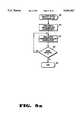
- FIG. 9Ais a flow chart showing a method used to open the switch circuit such that charge injection is reduced.
- FIG. 9Bis a flow chart showing a method used to close the switch circuit such that charge injection is reduced.
- FIG. 10is a timing diagram showing the operation of a switch circuit having three switches.
- FIG. 11shows a voltage-to-current converter of the improved I DDQ monitor circuit.
- FIG. 12shows a programmable current source of the improved I DDQ monitor circuit.
- FIG. 4shows automatic test equipment ("ATE") 399 that includes an improved I DDQ monitor circuit 400 for testing the quiescent power supply current I DDQ of the DUT 100.
- ATE 399is coupled to the DUT 100 for performing both functional testing and I DDQ testing of the DUT 100.
- the number of functional and I DDQ test vectors applied to the DUT 100is programmable and depends on the complexity and architecture of the DUT 100.
- FIG. 5shows the improved I DDQ monitor circuit for determining the quiescent power supply current I DDQ of a device under test.
- the I DDQ monitor circuit 400does not measure the change in voltage at the node 215. Instead, the I DDQ monitor circuit 400 detects whether the voltage at the node 215 increases or decreases over time. By detecting the slope polarity of the time rate of change, the quiescent power supply current I DDQ can be quickly determined in a qualitative manner. This helps to increase the speed of I DDQ testing by obviating the need for quantitative analysis of the voltage at node 215.
- the I DDQ monitor circuit 400includes a switch circuit 405, decoupling capacitor C2, a programmable current source 410, a voltage-to-current converter 407, a switch 409, a sample and hold circuit 420, a delay circuit 430, and a differential comparator 440.
- the switch circuit 405acts similarly to the switch 210 of the prior circuit but is designed to reduce charge injection that occurs when the power supply 205 is decoupled from the node 215.
- the voltage-to-current converter 407is also provided for further reducing the effects of charge injection due to switching.
- the switch circuit 405 and the voltage-to-current converter 407are described in greater detail below.
- the programmable current source 410is coupled to the node 215 for providing a reference current I REF to the node 215.
- the value of the reference current I REFis selectable by the user over a range of values.
- the reference currentis programmable from 0.0 to 1.023 milliamperes by 250 nanoampere steps.
- the accuracy of the programmable current source 410is ⁇ 700 nanoamperes.
- the switch circuit 405When the switch circuit 405 is switched off such that the power supply 205 is decoupled from node 215, the reference current I REF flows into the node 215 from the programmable current source, and a current flows out of the node 215 to ground via the DUT 100.
- the current flowing out of node 215is equal to the quiescent power supply current I DDQ for the DUT 100. If the reference current I REF is greater than the quiescent power supply current I DDQ for the DUT 100, the excess charge supplied to the node 215 by the programmable current source 410 is stored in the decoupling capacitor C2 and the parasitic DUT capacitance, which is shown as capacitor C DUT , such that the voltage at node 215 increases over time. If the quiescent power supply current I DDQ for the DUT 100 is greater than the reference current I REF , the decoupling capacitor C2 and the parasitic DUT capacitor C DUT discharge towards ground such that the voltage at node 215 decreases over time.
- the conduction path from the node 215 to ground provided by the DUT 100sinks more current than is provided by the programmable current source 410, the additional current is provided by the capacitors, and the node voltage drops. Conversely, if the conduction path provided by the DUT 100 sinks less current than is provided by the programmable current source 410, the excess charge is stored in capacitors, and the node voltage increases. If the reference current I REF is selected to be a value equal to the I DDQ value for a failing DUT, the value for I DDQ does not need to be quantitatively determined. It is sufficient to monitor whether the voltage at the node 215 increases or decreases.
- the value of the reference current I REFis selected to be equal to the I DDQ value for a failing DUT minus a guardband value, I r .
- the amount of guardband provided in the reference current I REFdetermines the resolution of the I DDQ monitor circuit and, ultimately, the I DDQ test cycle time. This is discussed in more detail below.
- the sample and hold circuit 420 and the comparator 440are provided for detecting whether the node voltage of node 215 increases or decreases.
- the switch circuit 405decouples the power supply 205 in response to an active I DDQ .sbsb.-- TEST signal.
- the active I DDQ .sbsb.-- TEST signalis also provided after a time delay to the sample and hold circuit 420.
- the delay circuit 430provides the time delay, which is of sufficient length to allow switching transients to settle.
- the sample and hold circuit 420receives the active I DDQ .sbsb.-- TEST signal
- the sample and hold circuit 420samples the node voltage V DUT at node 215 and holds the voltage as a reference voltage V REF .
- the reference voltage V REFis supplied by the sample and hold circuit 420 to the negative terminal of the comparator 440.
- the node voltage V DUTis coupled to the positive terminal of the comparator 440.
- the comparator 440outputs a Boolean logic signal when it determines the polarity of the time rate of change of the node voltage V DUT .
- the operation of the I DDQ monitoring circuit 400may be understood with reference to FIG. 6.
- standard functional testingis performed, and the logic of DUT 100 is toggled between states in response to the various input test vectors.
- an I DDQ test vectoris input to the DUT 100, causing a current transient.
- the active I DDQ .sbsb.-- TEST signalis provided to the switch circuit 405, causing the switch circuit 405 to decouple the power supply 205 from the node 215.
- the node voltage at node 215is sampled and held as the reference voltage V REF at time t2.
- the output of the comparator 440is checked to determine if the DUT 100 has passed the I DDQ test vector.
- a passing parthas a voltage V DUT that increases over time, wherein a failing part has a voltage that decreases over time.
- the length of the I DDQ test cycle, T cwhich begins at time t0 and ends at time t3, is determined by the following equation: ##EQU2## wherein V offset is the offset voltage for the comparator 440, I r is the guardband and the desired resolution for the I DDQ test, and T s is a fixed overhead time required by the on/off transition time of the switch circuit 405.
- the offset voltage V offset for the comparator 440is ⁇ 3 millivolts and the transition time T s for the switch circuit 405 is equal to one microsecond.
- the resolution I r of the I DDQ testcan be selected by the user of the ATE.
- the cycle time T c of the I DDQ testultimately depends on the selected resolution I r .
- the capacitance of decoupling capacitor C2is equal to 0.01 microfarads
- the resolution I ris 10 microamps
- the values of V offset and T sare those described above
- the I DDQ test cycle time T cis equal to four microseconds. If the resolution I r is changed to 20 microamps, the test cycle time T c is reduced to 2.5 microseconds.
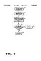
- FIG. 7is a flow chart showing a method implemented by the I DDQ monitor circuit of the present embodiment.
- an I DDQ test vectoris supplied to the inputs of the DUT 100 by the ATE.
- the switch circuit 405decouples the power supply 205 from the node 215 in response to an active I DDQ .sbsb.-- TEST signal received from the ATE.
- the sample and hold circuit 420samples the node voltage V DUT at the node 215 and holds the node voltage as the reference voltage V REF in response to receiving a delayed version of the active I DDQ .sbsb.-- TEST signal.
- the node voltage V DUTis compared to the reference voltage V REF . If the node voltage V DUT is greater than the reference voltage V REF , the comparator 440 indicates that the DUT passes the I DDQ test at step 625. If the node voltage V DUT is less than the reference voltage V REF , the comparator 440 indicates that the DUT fails the I DDQ test at step 630.
- FIG. 8shows the switch circuit 405 in greater detail.
- the switch circuit 405operates as a low impedance switch having reduced charge injection.
- Charge injectionis a common problem for FET switches that have a low impedance or "on resistance,” R on , when switched on.
- R onlow impedance or "on resistance”
- a parasitic capacitance between the gate and the source of a FET switchcauses the signal at the gate to be coupled to the source when the FET switch is switched off, thereby injecting noise at the source of the FET switch.
- the charge injectioncan be quite significant and can result in the changing of the DUT voltage, which can cause the logic state of the DUT to change.
- FIG. 8To reduce the effects of charge injection and shorten the I DDQ test cycle, the structure as shown in FIG. 8 is used.
- a multiplicity of FET switches, each having a unique "on resistance,” R onare coupled in parallel between the power supply 205 and the DUT 100.
- the switch SW1has the lowest “on resistance” value of R1.
- the FET switch SW2has the next lowest “on resistance” value of R2, and the FET switches from SW3 to SWN have successively greater "on resistance” values, from R3 to RN.
- Each of the FET switches SW1 to SWNis controlled independently of the other FET switches by supplying unique control signals to the gates of each of the FET switches.
- the control signalsmay be supplied externally by the ATE, or they may be generated internally by logic or a state machine in response to the I DDQ .sbsb.-- TEST signal.
- switch SW1is turned off first
- switch SW2is turned off second
- switch SW3is turned off third
- switch SW3+1is turned off next and so on until, finally, switch SWN is turned off.
- the switchesmay be any type of switch or combination of types of switches, including MOSFET, JFET, and BJT switches. The type of switch used is determined by the test requirements of the I DDQ monitor circuit 400.
- FIG. 9Ais a flow chart showing a method used by the switch circuit 405 to decouple the power supply 205 from the node 215.
- This method and equivalent methodsmay be implemented using logic, a state machine, or similar control circuit located externally to the IDDQ monitor circuit 400, within the I DDQ monitor circuit 400, or within the switch circuit 405.
- the ATEbegins the I DDQ test cycle by supplying an I DDQ test vector to the DUT 100.
- a first control signalis received by the lowest impedance switch of the switch circuit 405, and that switch is switched off.
- the switch having the next lowest impedance switchis switched off in response to its control signal.
- FIG. 9Bis a flow chart showing a method used by the switch circuit 405 to couple the power supply 205 to the node 215 at the end of the I DDQ test cycle.
- the I DDQ test cycleends.
- the highest impedance switchis switched on first in response to its own control signal.
- the next highest impedance switchis switched on in response to its control signal.
- FIG. 10is a timing diagram of the operation of a switch circuit 405 having three switches SW1-SW3.
- the ATE 399begins an I DDQ test cycle by delivering a logic high IDDQ -- TEST pulse to the I DDQ monitor circuit 400.
- the control signal CTR1goes high, switching off switch SW1.
- the predetermined intervalis calculated in light of the RC time constant of the node 215. The inclusion of the predetermined interval allows for the compensation of the charge injection of switching off a single switch.
- the duration of the predetermined intervalis 2 ⁇ S, but the interval may be changed as needed.
- control signal CTR3goes to a logic high level, and switch SW3 is switched off.
- Another predetermined intervalis provided between the time the control signal CTR3 goes high and the control signal MEAS high. During this predetermined interval, the switching transients are allowed to settle.
- the control signal MEASis generated by the delay circuit and supplied to the sample and hold circuit in response to the I DDQ .sbsb.-- TEST control signal.
- the time that MEAS remains highis equal to the test cycle time T c minus the fixed overhead time T s .
- T sis 12 ⁇ s and MEAS is asserted high for fifty times the IDDQ -- TEST pulse width.
- the sample and hold circuit 420samples the node voltage VDUT when MEAS goes high, and the output of the comparator 440 may be read by ATE 399 when MEAS goes low.
- the control signals CTR3, CTR2 and CTR1are asserted logic low in order. Again the predetermined intervals are provided between each event.
- FIG. 11shows the voltage to current converter in greater detail.
- the voltage-to-current converter 407also reduces the effects of charge injection due to switching, thus further reducing the I DDQ test cycle time.
- the voltage to current converter 407is a feedback circuit that detects the voltage transient at the node 215 caused by charge injection and injects a compensation current into the node 215 to compensate for the detected charge injection.
- the voltage-to-current converter 407operates between the times that the switch circuit 405 is switched off and the node voltage V DUT is first sampled.
- the switch 409disconnects the voltage to current converter from the node 215 before the node voltage V DUT is first sampled.
- the voltage-to-current converter 407is comprised generally of a non-inverting amplifier 1105, an inverting amplifier 1110, and a converting output stage 1115.
- the non-inverting amplifier 1105has a high input impedance and acts primarily as a buffer between the node 215 and the inverting amplifier 1110.
- the non-inverting amplifierhas unity gain.
- the inverting amplifier 1110has its input coupled to the output of the non-inverting amplifier 1105.
- the inverting amplifier 1110inverts the voltage output by the non-inverting amplifier.
- the inverting amplifier 1110also has unity gain; however, the gain of the inverting amplifier 1110 may be increased so long as the feedback loop is stabilized.
- the converting output stage 1115is coupled to the output of the inverting amplifier 1110.
- the converting output stage 1115converts the voltage output by the inverting amplifier 1110 to a compensation current that is supplied to the node 215.
- the non-inverting amplifier 1105may include an operational amplifier U1 coupled as non-inverting amplifier having its positive input coupled to the node 215 and its negative input coupled to its output.
- the inverting amplifier 1110may include an operational amplifier U2 coupled as an inverting AC amplifier having unity gain, wherein a resistor R1 is coupled between the negative input of the operational amplifier U2 and the output of the non-inverting amplifier 11105. Compensation capacitor C3 and the resistor R2 are coupled in parallel between the negative input of operational amplifier U2 and the output of operational amplifier U2.
- the compensation capacitor C3provides loop stability by compensating for phase shifts between the input of the voltage-to-current converter 407, which is coupled to node 215, and the output of the second pole of the switch 409, which is also coupled to node 215.
- the converting output stage 1115may include resistor R3 and capacitor C4.
- the operational amplifier U2outputs a voltage which is converted by the resistor R3 and the capacitor C4 into the compensation current which is supplied to the node 215 to compensate for charge injection.
- the operational amplifiers U1 and U2have a high slew rate, and the resistors and capacitors have low inductance to provide a very fast response for charge injection compensation. These characteristics of the operational amplifiers U1 and U2 reduce settling time and overvoltage/undervoltage transient stressing the DUT 100.
- FIG. 12shows the programmable current source in more detail.
- the programmable current source 410includes a random access memory (RAM) 1005, a digital-to-analog converter (DAC) 1010, and a current source 1015.
- the RAM 1005is used as a look-up table. When an input value is received by the RAM 1005 from the ATE, the RAM responds by performing a look-up and outputting the result of the look-up to the DAC 1005.
- the DACconverts the digital output signal of the RAM 1005 to an analog current.
- the current source 1015which may comprise a current mirror circuit, multiplies the current output by the DAC to produce the reference current I REF to the node 215.
Landscapes
- Engineering & Computer Science (AREA)
- General Engineering & Computer Science (AREA)
- Physics & Mathematics (AREA)
- General Physics & Mathematics (AREA)
- Tests Of Electronic Circuits (AREA)
Abstract
Description
Claims (19)
Priority Applications (1)
| Application Number | Priority Date | Filing Date | Title |
|---|---|---|---|
| US08/721,973US5694063A (en) | 1994-08-11 | 1996-09-27 | High speed IDDQ monitor circuit |
Applications Claiming Priority (3)
| Application Number | Priority Date | Filing Date | Title |
|---|---|---|---|
| US28891794A | 1994-08-11 | 1994-08-11 | |
| US57235295A | 1995-12-14 | 1995-12-14 | |
| US08/721,973US5694063A (en) | 1994-08-11 | 1996-09-27 | High speed IDDQ monitor circuit |
Related Parent Applications (1)
| Application Number | Title | Priority Date | Filing Date |
|---|---|---|---|
| US57235295AContinuation | 1994-08-11 | 1995-12-14 |
Publications (1)
| Publication Number | Publication Date |
|---|---|
| US5694063Atrue US5694063A (en) | 1997-12-02 |
Family
ID=26965330
Family Applications (1)
| Application Number | Title | Priority Date | Filing Date |
|---|---|---|---|
| US08/721,973Expired - LifetimeUS5694063A (en) | 1994-08-11 | 1996-09-27 | High speed IDDQ monitor circuit |
Country Status (1)
| Country | Link |
|---|---|
| US (1) | US5694063A (en) |
Cited By (67)
| Publication number | Priority date | Publication date | Assignee | Title |
|---|---|---|---|---|
| WO1999017179A1 (en)* | 1997-09-29 | 1999-04-08 | Credence Systems Corporation | Multiple output programmable reference voltage source |
| US6051442A (en)* | 1996-04-30 | 2000-04-18 | Kabushiki Kaisha Toshiba | CMOS integrated circuit device and its inspecting method and device |
| US6093212A (en)* | 1997-08-26 | 2000-07-25 | Ricoh Company, Ltd. | Method for selecting operation cycles of a semiconductor IC for performing an IDDQ test by using a simulation |
| WO2003073114A1 (en)* | 2002-02-22 | 2003-09-04 | Rutgers, The State University Of New Jersey | Method and system for graphical evaluation of iddq measurements |
| DE10248982A1 (en)* | 2002-08-30 | 2004-03-25 | Infineon Technologies Ag | Current consumption monitoring device for checking an electronic circuit's consumption comprises a capacitor arranged in parallel to the circuit to be monitored together with a switch for isolating the so created parallel circuit |
| WO2004027438A1 (en)* | 2002-09-20 | 2004-04-01 | Koninklijke Philips Electronics N.V. | Method and apparatus for determining iddq |
| US6810344B1 (en)* | 1999-11-11 | 2004-10-26 | Kabushiki Kaisha Toshiba | Semiconductor testing method and semiconductor testing apparatus for semiconductor devices, and program for executing semiconductor testing method |
| US20050077906A1 (en)* | 2003-10-10 | 2005-04-14 | Baumgartner Richard A. | Systems and methods for measuring picoampere current levels |
| US20050146342A1 (en)* | 2004-01-02 | 2005-07-07 | Jang Jin-Mo | Apparatus for generating test stimulus signal having current regardless of internal impedance changes of device under test |
| US20050271136A1 (en)* | 2004-05-18 | 2005-12-08 | Chung David K | Decision feedback equalizer circuit |
| US20070170931A1 (en)* | 2006-01-20 | 2007-07-26 | Snyder Warren S | Successive approximate capacitance measurement circuit |
| US20090073780A1 (en)* | 2007-07-04 | 2009-03-19 | Samsung Electronics Co., Ltd. | Memory device for detecting bit line leakage current and method thereof |
| US20090212851A1 (en)* | 2008-02-27 | 2009-08-27 | Osamu Yamashita | Power supply unit |
| US7737724B2 (en) | 2007-04-17 | 2010-06-15 | Cypress Semiconductor Corporation | Universal digital block interconnection and channel routing |
| US7761845B1 (en) | 2002-09-09 | 2010-07-20 | Cypress Semiconductor Corporation | Method for parameterizing a user module |
| US7765095B1 (en) | 2000-10-26 | 2010-07-27 | Cypress Semiconductor Corporation | Conditional branching in an in-circuit emulation system |
| US7770113B1 (en) | 2001-11-19 | 2010-08-03 | Cypress Semiconductor Corporation | System and method for dynamically generating a configuration datasheet |
| US7774190B1 (en) | 2001-11-19 | 2010-08-10 | Cypress Semiconductor Corporation | Sleep and stall in an in-circuit emulation system |
| US7825688B1 (en) | 2000-10-26 | 2010-11-02 | Cypress Semiconductor Corporation | Programmable microcontroller architecture(mixed analog/digital) |
| US7844437B1 (en) | 2001-11-19 | 2010-11-30 | Cypress Semiconductor Corporation | System and method for performing next placements and pruning of disallowed placements for programming an integrated circuit |
| US7893724B2 (en) | 2004-03-25 | 2011-02-22 | Cypress Semiconductor Corporation | Method and circuit for rapid alignment of signals |
| US20110093222A1 (en)* | 2009-10-19 | 2011-04-21 | Hong Fu Jin Precision Industry (Shenzhen) Co., Ltd. | Power cycling test apparatus |
| US8026739B2 (en) | 2007-04-17 | 2011-09-27 | Cypress Semiconductor Corporation | System level interconnect with programmable switching |
| US8040266B2 (en) | 2007-04-17 | 2011-10-18 | Cypress Semiconductor Corporation | Programmable sigma-delta analog-to-digital converter |
| US8049569B1 (en) | 2007-09-05 | 2011-11-01 | Cypress Semiconductor Corporation | Circuit and method for improving the accuracy of a crystal-less oscillator having dual-frequency modes |
| US8069405B1 (en) | 2001-11-19 | 2011-11-29 | Cypress Semiconductor Corporation | User interface for efficiently browsing an electronic document using data-driven tabs |
| US8069428B1 (en) | 2001-10-24 | 2011-11-29 | Cypress Semiconductor Corporation | Techniques for generating microcontroller configuration information |
| US8069436B2 (en) | 2004-08-13 | 2011-11-29 | Cypress Semiconductor Corporation | Providing hardware independence to automate code generation of processing device firmware |
| US8067948B2 (en) | 2006-03-27 | 2011-11-29 | Cypress Semiconductor Corporation | Input/output multiplexer bus |
| US8078970B1 (en) | 2001-11-09 | 2011-12-13 | Cypress Semiconductor Corporation | Graphical user interface with user-selectable list-box |
| US8078894B1 (en) | 2007-04-25 | 2011-12-13 | Cypress Semiconductor Corporation | Power management architecture, method and configuration system |
| US8085067B1 (en) | 2005-12-21 | 2011-12-27 | Cypress Semiconductor Corporation | Differential-to-single ended signal converter circuit and method |
| US8085100B2 (en) | 2005-02-04 | 2011-12-27 | Cypress Semiconductor Corporation | Poly-phase frequency synthesis oscillator |
| US8089461B2 (en) | 2005-06-23 | 2012-01-03 | Cypress Semiconductor Corporation | Touch wake for electronic devices |
| US8089289B1 (en) | 2007-07-03 | 2012-01-03 | Cypress Semiconductor Corporation | Capacitive field sensor with sigma-delta modulator |
| US8089288B1 (en) | 2006-11-16 | 2012-01-03 | Cypress Semiconductor Corporation | Charge accumulation capacitance sensor with linear transfer characteristic |
| US8092083B2 (en) | 2007-04-17 | 2012-01-10 | Cypress Semiconductor Corporation | Temperature sensor with digital bandgap |
| US8103496B1 (en) | 2000-10-26 | 2012-01-24 | Cypress Semicondutor Corporation | Breakpoint control in an in-circuit emulation system |
| US8103497B1 (en) | 2002-03-28 | 2012-01-24 | Cypress Semiconductor Corporation | External interface for event architecture |
| US8120408B1 (en) | 2005-05-05 | 2012-02-21 | Cypress Semiconductor Corporation | Voltage controlled oscillator delay cell and method |
| US8130025B2 (en) | 2007-04-17 | 2012-03-06 | Cypress Semiconductor Corporation | Numerical band gap |
| US8149048B1 (en) | 2000-10-26 | 2012-04-03 | Cypress Semiconductor Corporation | Apparatus and method for programmable power management in a programmable analog circuit block |
| US8160864B1 (en) | 2000-10-26 | 2012-04-17 | Cypress Semiconductor Corporation | In-circuit emulator and pod synchronized boot |
| US8169238B1 (en) | 2007-07-03 | 2012-05-01 | Cypress Semiconductor Corporation | Capacitance to frequency converter |
| US8176296B2 (en) | 2000-10-26 | 2012-05-08 | Cypress Semiconductor Corporation | Programmable microcontroller architecture |
| US8286125B2 (en) | 2004-08-13 | 2012-10-09 | Cypress Semiconductor Corporation | Model for a hardware device-independent method of defining embedded firmware for programmable systems |
| US8321174B1 (en) | 2008-09-26 | 2012-11-27 | Cypress Semiconductor Corporation | System and method to measure capacitance of capacitive sensor array |
| US8358142B2 (en) | 2008-02-27 | 2013-01-22 | Cypress Semiconductor Corporation | Methods and circuits for measuring mutual and self capacitance |
| US8402313B1 (en) | 2002-05-01 | 2013-03-19 | Cypress Semiconductor Corporation | Reconfigurable testing system and method |
| US8493351B2 (en) | 2006-03-30 | 2013-07-23 | Cypress Semiconductor Corporation | Apparatus and method for reducing average scan rate to detect a conductive object on a sensing device |
| US8499270B1 (en) | 2007-04-25 | 2013-07-30 | Cypress Semiconductor Corporation | Configuration of programmable IC design elements |
| US8516025B2 (en) | 2007-04-17 | 2013-08-20 | Cypress Semiconductor Corporation | Clock driven dynamic datapath chaining |
| US8525798B2 (en) | 2008-01-28 | 2013-09-03 | Cypress Semiconductor Corporation | Touch sensing |
| US8527949B1 (en) | 2001-11-19 | 2013-09-03 | Cypress Semiconductor Corporation | Graphical user interface for dynamically reconfiguring a programmable device |
| US8547114B2 (en) | 2006-11-14 | 2013-10-01 | Cypress Semiconductor Corporation | Capacitance to code converter with sigma-delta modulator |
| US8564313B1 (en) | 2007-07-03 | 2013-10-22 | Cypress Semiconductor Corporation | Capacitive field sensor with sigma-delta modulator |
| US8570052B1 (en) | 2008-02-27 | 2013-10-29 | Cypress Semiconductor Corporation | Methods and circuits for measuring mutual and self capacitance |
| US8922271B1 (en)* | 2013-07-29 | 2014-12-30 | Micrel, Inc. | Programmable high current voltage supply for automatic test equipment |
| US8976124B1 (en) | 2007-05-07 | 2015-03-10 | Cypress Semiconductor Corporation | Reducing sleep current in a capacitance sensing system |
| US9104273B1 (en) | 2008-02-29 | 2015-08-11 | Cypress Semiconductor Corporation | Multi-touch sensing method |
| US9417728B2 (en) | 2009-07-28 | 2016-08-16 | Parade Technologies, Ltd. | Predictive touch surface scanning |
| US9448964B2 (en) | 2009-05-04 | 2016-09-20 | Cypress Semiconductor Corporation | Autonomous control in a programmable system |
| US9564902B2 (en) | 2007-04-17 | 2017-02-07 | Cypress Semiconductor Corporation | Dynamically configurable and re-configurable data path |
| US9588171B2 (en) | 2012-05-16 | 2017-03-07 | Infineon Technologies Ag | System and method for testing an integrated circuit |
| US9720805B1 (en) | 2007-04-25 | 2017-08-01 | Cypress Semiconductor Corporation | System and method for controlling a target device |
| US10698662B2 (en) | 2001-11-15 | 2020-06-30 | Cypress Semiconductor Corporation | System providing automatic source code generation for personalization and parameterization of user modules |
| US20240110966A1 (en)* | 2022-09-30 | 2024-04-04 | Psemi Corporation | Current measurement for defect detection |
Citations (9)
| Publication number | Priority date | Publication date | Assignee | Title |
|---|---|---|---|---|
| US4782290A (en)* | 1984-10-04 | 1988-11-01 | Sony/Tektronix, Inc. | Apparatus for measuring characteristics or electronic devices |
| US5059889A (en)* | 1990-03-08 | 1991-10-22 | Texas Instruments Incorporated | Parametric measurement unit/device power supply for semiconductor test system |
| US5128567A (en)* | 1988-05-02 | 1992-07-07 | Kabushiki Kaisha Toshiba | Output circuit of semiconductor integrated circuit with reduced power source line noise |
| US5216289A (en)* | 1991-10-24 | 1993-06-01 | Intel Corporation | Asynchronous reset scheme for ultra-low noise port tri-state output driver circuit |
| US5319258A (en)* | 1991-07-16 | 1994-06-07 | Samsung Semiconductor, Inc. | Programmable output drive circuit |
| US5332973A (en)* | 1992-05-01 | 1994-07-26 | The University Of Manitoba | Built-in fault testing of integrated circuits |
| US5371457A (en)* | 1991-02-12 | 1994-12-06 | Lipp; Robert J. | Method and apparatus to test for current in an integrated circuit |
| US5398318A (en)* | 1989-11-02 | 1995-03-14 | Hitachi, Ltd. | High speed, low noise output buffer with non-identical pairs of output transistors |
| US5412263A (en)* | 1992-09-30 | 1995-05-02 | At&T Corp. | Multiple control voltage generation for MOSFET resistors |
- 1996
- 1996-09-27USUS08/721,973patent/US5694063A/ennot_activeExpired - Lifetime
Patent Citations (9)
| Publication number | Priority date | Publication date | Assignee | Title |
|---|---|---|---|---|
| US4782290A (en)* | 1984-10-04 | 1988-11-01 | Sony/Tektronix, Inc. | Apparatus for measuring characteristics or electronic devices |
| US5128567A (en)* | 1988-05-02 | 1992-07-07 | Kabushiki Kaisha Toshiba | Output circuit of semiconductor integrated circuit with reduced power source line noise |
| US5398318A (en)* | 1989-11-02 | 1995-03-14 | Hitachi, Ltd. | High speed, low noise output buffer with non-identical pairs of output transistors |
| US5059889A (en)* | 1990-03-08 | 1991-10-22 | Texas Instruments Incorporated | Parametric measurement unit/device power supply for semiconductor test system |
| US5371457A (en)* | 1991-02-12 | 1994-12-06 | Lipp; Robert J. | Method and apparatus to test for current in an integrated circuit |
| US5319258A (en)* | 1991-07-16 | 1994-06-07 | Samsung Semiconductor, Inc. | Programmable output drive circuit |
| US5216289A (en)* | 1991-10-24 | 1993-06-01 | Intel Corporation | Asynchronous reset scheme for ultra-low noise port tri-state output driver circuit |
| US5332973A (en)* | 1992-05-01 | 1994-07-26 | The University Of Manitoba | Built-in fault testing of integrated circuits |
| US5412263A (en)* | 1992-09-30 | 1995-05-02 | At&T Corp. | Multiple control voltage generation for MOSFET resistors |
Non-Patent Citations (35)
| Title |
|---|
| C. Chen & J. Abrahm, High Quality Tests For Switch Level Circuits Using Current And Logic Test Generation Algorithms , IEEE, 1991 Int l Test Conference, pp. 615 622.* |
| C. Chen & J. Abrahm, High Quality Tests For Switch-Level Circuits Using Current And Logic Test Generation Algorithms, IEEE, 1991 Int'l Test Conference, pp. 615-622. |
| C. Crapuchettes, Testing CMOS Idd on Large Devices , IEEE, 1987 Int l Test Conference, pp. 310 315.* |
| C. Crapuchettes, Testing CMOS Idd on Large Devices, IEEE, 1987 Int'l Test Conference, pp. 310-315. |
| E. Vandris & G. Sobelman, A Mixed Functional/Iddq Testing Methodology For CMOS Transistor Faults , IEEE, 1991 Int l Test Conference, pp. 608 614.* |
| E. Vandris & G. Sobelman, A Mixed Functional/Iddq Testing Methodology For CMOS Transistor Faults, IEEE, 1991 Int'l Test Conference, pp. 608-614. |
| J. Soden, R. Fritzemeier & C. Hawkins, Zero Defects or Zero Stuck At Faults CMOS IC Process Improvement With Iddq , IEEE, 1990 Int l Test Conference, pp. 255 256.* |
| J. Soden, R. Fritzemeier & C. Hawkins, Zero Defects or Zero Stuck-At Faults--CMOS IC Process Improvement With Iddq, IEEE, 1990 Int'l Test Conference, pp. 255-256. |
| K. Baker & B. Verhelst, Iddq Testing Because "Zero Defects Isn't Enough", IEEE, 1990 Int'l Test Conference, pp. 253-524. |
| K. Baker & B. Verhelst, Iddq Testing Because Zero Defects Isn t Enough , IEEE, 1990 Int l Test Conference, pp. 253 524.* |
| K. M. Wallquist, A. W. Righter, and C.F. Hawkins, A General Purpose IDDQ Measurement Circuit , IEEE, 1993 Int l Test Conference, pp. 642 651.* |
| K. M. Wallquist, A. W. Righter, and C.F. Hawkins, A General Purpose IDDQ Measurement Circuit, IEEE, 1993 Int'l Test Conference, pp. 642-651. |
| L. Horning, J. Soden, R. Fritzemeier & C. Hawkins, Measurements of Quiescent Power Supply Current For CMOS ICs In Production Testing , IEEE, 1987 Int l Test Conference, pp. 300 309.* |
| L. Horning, J. Soden, R. Fritzemeier & C. Hawkins, Measurements of Quiescent Power Supply Current For CMOS ICs In Production Testing, IEEE, 1987 Int'l Test Conference, pp. 300-309. |
| M. Keating & D. Meyer, A New Approach To Dynamic Idd Testing , IEEE, 1987 Int l Test Conference, pp. 316 321.* |
| M. Keating & D. Meyer, A New Approach To Dynamic Idd Testing, IEEE, 1987 Int'l Test Conference, pp. 316-321. |
| PCT International Search Report, 5 pages.* |
| R. Aitken, A Comparison Of Defect Models For Fault Location With Iddq Measurements , IEEE, 1992 Int l Test Conference, pp. 778 787.* |
| R. Aitken, A Comparison Of Defect Models For Fault Location With Iddq Measurements, IEEE, 1992 Int'l Test Conference, pp. 778-787. |
| R. Aitken, Fault Location With Current Monitoring , IEEE, 1991 Int l Test Conference, pp. 623 632.* |
| R. Aitken, Fault Location With Current Monitoring, IEEE, 1991 Int'l Test Conference, pp. 623-632. |
| R. Gulati, W. Mao & D. Goel, Detection Of "Undetectable" Faults Using Iddq Testing, IEEE, 1992 Int'l Test Conference, pp. 770-775. |
| R. Gulati, W. Mao & D. Goel, Detection Of Undetectable Faults Using Iddq Testing , IEEE, 1992 Int l Test Conference, pp. 770 775.* |
| R. Kapur, J. Park & M. Mercer, All Tests For A Fault Are Not Equally Valuable For Defect Detection , IEEE, 1992 Int l Test Conference, pp. 762 769.* |
| R. Kapur, J. Park & M. Mercer, All Tests For A Fault Are Not Equally Valuable For Defect Detection, IEEE, 1992 Int'l Test Conference, pp. 762-769. |
| R. Rodriguez Montanes, E. M. J. G. Bruls & J. Figueras, Bridging Defects Resistance Measurements In A CMOS Process , IEEE, 1992 Int l Test Conference, pp. 892 899.* |
| R. Rodriguez-Montanes, E. M. J. G. Bruls & J. Figueras, Bridging Defects Resistance Measurements In A CMOS Process, IEEE, 1992 Int'l Test Conference, pp. 892-899. |
| S. Bollinger & S. Midkiff, On Test Generation For Iddq Testing Of Bridging Faults In CMOS Circuits , IEEE, 1991 Int l Test Conference, pp. 598 607.* |
| S. Bollinger & S. Midkiff, On Test Generation For Iddq Testing Of Bridging Faults In CMOS Circuits, IEEE, 1991 Int'l Test Conference, pp. 598-607. |
| S. McEuen, Why IDDQ , IEEE, 1990 Int l Test Conference, p. 252.* |
| S. McEuen, Why IDDQ, IEEE, 1990 Int'l Test Conference, p. 252. |
| W. Maly, Current Testing , IEEE, 1990 Int l Test Conference, p. 257.* |
| W. Maly, Current Testing, IEEE, 1990 Int'l Test Conference, p. 257. |
| Y. Miura & K. Kinoshita, Circuit Design For Built In Current Testing , IEEE, 1992 Int l Test Conference, pp. 873 881.* |
| Y. Miura & K. Kinoshita, Circuit Design For Built-In Current Testing, IEEE, 1992 Int'l Test Conference, pp. 873-881. |
Cited By (115)
| Publication number | Priority date | Publication date | Assignee | Title |
|---|---|---|---|---|
| US6051442A (en)* | 1996-04-30 | 2000-04-18 | Kabushiki Kaisha Toshiba | CMOS integrated circuit device and its inspecting method and device |
| US6187602B1 (en) | 1996-04-30 | 2001-02-13 | Kabushiki Kaisha Toshiba | CMOS integrated circuit device and its inspecting method and device |
| US6093212A (en)* | 1997-08-26 | 2000-07-25 | Ricoh Company, Ltd. | Method for selecting operation cycles of a semiconductor IC for performing an IDDQ test by using a simulation |
| US5905403A (en)* | 1997-09-29 | 1999-05-18 | Credence Systems Corporation | Multiple output programmable reference voltage source |
| WO1999017179A1 (en)* | 1997-09-29 | 1999-04-08 | Credence Systems Corporation | Multiple output programmable reference voltage source |
| US6810344B1 (en)* | 1999-11-11 | 2004-10-26 | Kabushiki Kaisha Toshiba | Semiconductor testing method and semiconductor testing apparatus for semiconductor devices, and program for executing semiconductor testing method |
| US9766650B2 (en) | 2000-10-26 | 2017-09-19 | Cypress Semiconductor Corporation | Microcontroller programmable system on a chip with programmable interconnect |
| US8358150B1 (en) | 2000-10-26 | 2013-01-22 | Cypress Semiconductor Corporation | Programmable microcontroller architecture(mixed analog/digital) |
| US8555032B2 (en) | 2000-10-26 | 2013-10-08 | Cypress Semiconductor Corporation | Microcontroller programmable system on a chip with programmable interconnect |
| US8736303B2 (en) | 2000-10-26 | 2014-05-27 | Cypress Semiconductor Corporation | PSOC architecture |
| US9843327B1 (en) | 2000-10-26 | 2017-12-12 | Cypress Semiconductor Corporation | PSOC architecture |
| US8149048B1 (en) | 2000-10-26 | 2012-04-03 | Cypress Semiconductor Corporation | Apparatus and method for programmable power management in a programmable analog circuit block |
| US8160864B1 (en) | 2000-10-26 | 2012-04-17 | Cypress Semiconductor Corporation | In-circuit emulator and pod synchronized boot |
| US10725954B2 (en) | 2000-10-26 | 2020-07-28 | Monterey Research, Llc | Microcontroller programmable system on a chip |
| US7825688B1 (en) | 2000-10-26 | 2010-11-02 | Cypress Semiconductor Corporation | Programmable microcontroller architecture(mixed analog/digital) |
| US7765095B1 (en) | 2000-10-26 | 2010-07-27 | Cypress Semiconductor Corporation | Conditional branching in an in-circuit emulation system |
| US8103496B1 (en) | 2000-10-26 | 2012-01-24 | Cypress Semicondutor Corporation | Breakpoint control in an in-circuit emulation system |
| US8176296B2 (en) | 2000-10-26 | 2012-05-08 | Cypress Semiconductor Corporation | Programmable microcontroller architecture |
| US10020810B2 (en) | 2000-10-26 | 2018-07-10 | Cypress Semiconductor Corporation | PSoC architecture |
| US10261932B2 (en) | 2000-10-26 | 2019-04-16 | Cypress Semiconductor Corporation | Microcontroller programmable system on a chip |
| US10248604B2 (en) | 2000-10-26 | 2019-04-02 | Cypress Semiconductor Corporation | Microcontroller programmable system on a chip |
| US10466980B2 (en) | 2001-10-24 | 2019-11-05 | Cypress Semiconductor Corporation | Techniques for generating microcontroller configuration information |
| US8069428B1 (en) | 2001-10-24 | 2011-11-29 | Cypress Semiconductor Corporation | Techniques for generating microcontroller configuration information |
| US8793635B1 (en) | 2001-10-24 | 2014-07-29 | Cypress Semiconductor Corporation | Techniques for generating microcontroller configuration information |
| US8078970B1 (en) | 2001-11-09 | 2011-12-13 | Cypress Semiconductor Corporation | Graphical user interface with user-selectable list-box |
| US10698662B2 (en) | 2001-11-15 | 2020-06-30 | Cypress Semiconductor Corporation | System providing automatic source code generation for personalization and parameterization of user modules |
| US8533677B1 (en) | 2001-11-19 | 2013-09-10 | Cypress Semiconductor Corporation | Graphical user interface for dynamically reconfiguring a programmable device |
| US8069405B1 (en) | 2001-11-19 | 2011-11-29 | Cypress Semiconductor Corporation | User interface for efficiently browsing an electronic document using data-driven tabs |
| US7770113B1 (en) | 2001-11-19 | 2010-08-03 | Cypress Semiconductor Corporation | System and method for dynamically generating a configuration datasheet |
| US7774190B1 (en) | 2001-11-19 | 2010-08-10 | Cypress Semiconductor Corporation | Sleep and stall in an in-circuit emulation system |
| US8370791B2 (en) | 2001-11-19 | 2013-02-05 | Cypress Semiconductor Corporation | System and method for performing next placements and pruning of disallowed placements for programming an integrated circuit |
| US7844437B1 (en) | 2001-11-19 | 2010-11-30 | Cypress Semiconductor Corporation | System and method for performing next placements and pruning of disallowed placements for programming an integrated circuit |
| US8527949B1 (en) | 2001-11-19 | 2013-09-03 | Cypress Semiconductor Corporation | Graphical user interface for dynamically reconfiguring a programmable device |
| US6812724B2 (en) | 2002-02-22 | 2004-11-02 | Lan Rao | Method and system for graphical evaluation of IDDQ measurements |
| US20030171896A1 (en)* | 2002-02-22 | 2003-09-11 | Lan Rao | Method and system for graphical evaluation of IDDQ measurements |
| WO2003073114A1 (en)* | 2002-02-22 | 2003-09-04 | Rutgers, The State University Of New Jersey | Method and system for graphical evaluation of iddq measurements |
| US8103497B1 (en) | 2002-03-28 | 2012-01-24 | Cypress Semiconductor Corporation | External interface for event architecture |
| US8402313B1 (en) | 2002-05-01 | 2013-03-19 | Cypress Semiconductor Corporation | Reconfigurable testing system and method |
| DE10248982A1 (en)* | 2002-08-30 | 2004-03-25 | Infineon Technologies Ag | Current consumption monitoring device for checking an electronic circuit's consumption comprises a capacitor arranged in parallel to the circuit to be monitored together with a switch for isolating the so created parallel circuit |
| DE10248982B4 (en)* | 2002-08-30 | 2006-10-26 | Infineon Technologies Ag | Device and method for monitoring the current consumption of a circuit arrangement |
| US7761845B1 (en) | 2002-09-09 | 2010-07-20 | Cypress Semiconductor Corporation | Method for parameterizing a user module |
| WO2004027438A1 (en)* | 2002-09-20 | 2004-04-01 | Koninklijke Philips Electronics N.V. | Method and apparatus for determining iddq |
| US6998850B2 (en)* | 2003-10-10 | 2006-02-14 | Agilent Technologies, Inc. | Systems and methods for measuring picoampere current levels |
| US20050077906A1 (en)* | 2003-10-10 | 2005-04-14 | Baumgartner Richard A. | Systems and methods for measuring picoampere current levels |
| US7268573B2 (en)* | 2004-01-02 | 2007-09-11 | Samsung Electronics Co., Ltd. | Apparatus for generating test stimulus signal having current regardless of internal impedance changes of device under test |
| US20050146342A1 (en)* | 2004-01-02 | 2005-07-07 | Jang Jin-Mo | Apparatus for generating test stimulus signal having current regardless of internal impedance changes of device under test |
| US7893724B2 (en) | 2004-03-25 | 2011-02-22 | Cypress Semiconductor Corporation | Method and circuit for rapid alignment of signals |
| US7839922B2 (en)* | 2004-05-18 | 2010-11-23 | Broadcom Corporation | Decision feedback equalizer circuit |
| US20110044384A1 (en)* | 2004-05-18 | 2011-02-24 | Broadcom Corporation | Decision feedback equalizer circuit |
| US20050271136A1 (en)* | 2004-05-18 | 2005-12-08 | Chung David K | Decision feedback equalizer circuit |
| US8283982B2 (en) | 2004-05-18 | 2012-10-09 | Broadcom Corporation | Decision feedback equalizer circuit |
| US8069436B2 (en) | 2004-08-13 | 2011-11-29 | Cypress Semiconductor Corporation | Providing hardware independence to automate code generation of processing device firmware |
| US8286125B2 (en) | 2004-08-13 | 2012-10-09 | Cypress Semiconductor Corporation | Model for a hardware device-independent method of defining embedded firmware for programmable systems |
| US8085100B2 (en) | 2005-02-04 | 2011-12-27 | Cypress Semiconductor Corporation | Poly-phase frequency synthesis oscillator |
| US8120408B1 (en) | 2005-05-05 | 2012-02-21 | Cypress Semiconductor Corporation | Voltage controlled oscillator delay cell and method |
| US8089461B2 (en) | 2005-06-23 | 2012-01-03 | Cypress Semiconductor Corporation | Touch wake for electronic devices |
| US8085067B1 (en) | 2005-12-21 | 2011-12-27 | Cypress Semiconductor Corporation | Differential-to-single ended signal converter circuit and method |
| US20070170931A1 (en)* | 2006-01-20 | 2007-07-26 | Snyder Warren S | Successive approximate capacitance measurement circuit |
| US7312616B2 (en)* | 2006-01-20 | 2007-12-25 | Cypress Semiconductor Corporation | Successive approximate capacitance measurement circuit |
| US7884621B2 (en) | 2006-01-20 | 2011-02-08 | Cypress Semiconductor Corporation | Successive approximate capacitance measurement circuit |
| US8067948B2 (en) | 2006-03-27 | 2011-11-29 | Cypress Semiconductor Corporation | Input/output multiplexer bus |
| US8717042B1 (en) | 2006-03-27 | 2014-05-06 | Cypress Semiconductor Corporation | Input/output multiplexer bus |
| US8493351B2 (en) | 2006-03-30 | 2013-07-23 | Cypress Semiconductor Corporation | Apparatus and method for reducing average scan rate to detect a conductive object on a sensing device |
| US9152284B1 (en) | 2006-03-30 | 2015-10-06 | Cypress Semiconductor Corporation | Apparatus and method for reducing average scan rate to detect a conductive object on a sensing device |
| US9166621B2 (en) | 2006-11-14 | 2015-10-20 | Cypress Semiconductor Corporation | Capacitance to code converter with sigma-delta modulator |
| US9154160B2 (en) | 2006-11-14 | 2015-10-06 | Cypress Semiconductor Corporation | Capacitance to code converter with sigma-delta modulator |
| US8547114B2 (en) | 2006-11-14 | 2013-10-01 | Cypress Semiconductor Corporation | Capacitance to code converter with sigma-delta modulator |
| US8089288B1 (en) | 2006-11-16 | 2012-01-03 | Cypress Semiconductor Corporation | Charge accumulation capacitance sensor with linear transfer characteristic |
| US8130025B2 (en) | 2007-04-17 | 2012-03-06 | Cypress Semiconductor Corporation | Numerical band gap |
| US8482313B2 (en) | 2007-04-17 | 2013-07-09 | Cypress Semiconductor Corporation | Universal digital block interconnection and channel routing |
| US8516025B2 (en) | 2007-04-17 | 2013-08-20 | Cypress Semiconductor Corporation | Clock driven dynamic datapath chaining |
| US8476928B1 (en) | 2007-04-17 | 2013-07-02 | Cypress Semiconductor Corporation | System level interconnect with programmable switching |
| US8026739B2 (en) | 2007-04-17 | 2011-09-27 | Cypress Semiconductor Corporation | System level interconnect with programmable switching |
| US8040266B2 (en) | 2007-04-17 | 2011-10-18 | Cypress Semiconductor Corporation | Programmable sigma-delta analog-to-digital converter |
| US8092083B2 (en) | 2007-04-17 | 2012-01-10 | Cypress Semiconductor Corporation | Temperature sensor with digital bandgap |
| US7737724B2 (en) | 2007-04-17 | 2010-06-15 | Cypress Semiconductor Corporation | Universal digital block interconnection and channel routing |
| US9564902B2 (en) | 2007-04-17 | 2017-02-07 | Cypress Semiconductor Corporation | Dynamically configurable and re-configurable data path |
| US8078894B1 (en) | 2007-04-25 | 2011-12-13 | Cypress Semiconductor Corporation | Power management architecture, method and configuration system |
| US9720805B1 (en) | 2007-04-25 | 2017-08-01 | Cypress Semiconductor Corporation | System and method for controlling a target device |
| US8909960B1 (en) | 2007-04-25 | 2014-12-09 | Cypress Semiconductor Corporation | Power management architecture, method and configuration system |
| US8499270B1 (en) | 2007-04-25 | 2013-07-30 | Cypress Semiconductor Corporation | Configuration of programmable IC design elements |
| US8976124B1 (en) | 2007-05-07 | 2015-03-10 | Cypress Semiconductor Corporation | Reducing sleep current in a capacitance sensing system |
| US10788937B2 (en) | 2007-05-07 | 2020-09-29 | Cypress Semiconductor Corporation | Reducing sleep current in a capacitance sensing system |
| US12181943B2 (en) | 2007-05-07 | 2024-12-31 | Cypress Semiconductor Corporation | Reducing sleep current in a capacitance sensing system |
| US8536902B1 (en)* | 2007-07-03 | 2013-09-17 | Cypress Semiconductor Corporation | Capacitance to frequency converter |
| US8570053B1 (en) | 2007-07-03 | 2013-10-29 | Cypress Semiconductor Corporation | Capacitive field sensor with sigma-delta modulator |
| US8564313B1 (en) | 2007-07-03 | 2013-10-22 | Cypress Semiconductor Corporation | Capacitive field sensor with sigma-delta modulator |
| US8169238B1 (en) | 2007-07-03 | 2012-05-01 | Cypress Semiconductor Corporation | Capacitance to frequency converter |
| US8089289B1 (en) | 2007-07-03 | 2012-01-03 | Cypress Semiconductor Corporation | Capacitive field sensor with sigma-delta modulator |
| US20090073780A1 (en)* | 2007-07-04 | 2009-03-19 | Samsung Electronics Co., Ltd. | Memory device for detecting bit line leakage current and method thereof |
| US8049569B1 (en) | 2007-09-05 | 2011-11-01 | Cypress Semiconductor Corporation | Circuit and method for improving the accuracy of a crystal-less oscillator having dual-frequency modes |
| US9760192B2 (en) | 2008-01-28 | 2017-09-12 | Cypress Semiconductor Corporation | Touch sensing |
| US8525798B2 (en) | 2008-01-28 | 2013-09-03 | Cypress Semiconductor Corporation | Touch sensing |
| US8358142B2 (en) | 2008-02-27 | 2013-01-22 | Cypress Semiconductor Corporation | Methods and circuits for measuring mutual and self capacitance |
| US9494628B1 (en) | 2008-02-27 | 2016-11-15 | Parade Technologies, Ltd. | Methods and circuits for measuring mutual and self capacitance |
| US9423427B2 (en) | 2008-02-27 | 2016-08-23 | Parade Technologies, Ltd. | Methods and circuits for measuring mutual and self capacitance |
| US20090212851A1 (en)* | 2008-02-27 | 2009-08-27 | Osamu Yamashita | Power supply unit |
| US8570052B1 (en) | 2008-02-27 | 2013-10-29 | Cypress Semiconductor Corporation | Methods and circuits for measuring mutual and self capacitance |
| US8004349B2 (en)* | 2008-02-27 | 2011-08-23 | Renesas Electronics Corporation | Power supply unit |
| US20110063021A1 (en)* | 2008-02-27 | 2011-03-17 | Renesas Electronics Corporation | Power supply unit |
| US7859324B2 (en)* | 2008-02-27 | 2010-12-28 | Renesas Electronics Corporation | Power supply unit |
| US8692563B1 (en) | 2008-02-27 | 2014-04-08 | Cypress Semiconductor Corporation | Methods and circuits for measuring mutual and self capacitance |
| US9104273B1 (en) | 2008-02-29 | 2015-08-11 | Cypress Semiconductor Corporation | Multi-touch sensing method |
| US10386969B1 (en) | 2008-09-26 | 2019-08-20 | Cypress Semiconductor Corporation | System and method to measure capacitance of capacitive sensor array |
| US11029795B2 (en) | 2008-09-26 | 2021-06-08 | Cypress Semiconductor Corporation | System and method to measure capacitance of capacitive sensor array |
| US8321174B1 (en) | 2008-09-26 | 2012-11-27 | Cypress Semiconductor Corporation | System and method to measure capacitance of capacitive sensor array |
| US9448964B2 (en) | 2009-05-04 | 2016-09-20 | Cypress Semiconductor Corporation | Autonomous control in a programmable system |
| US9417728B2 (en) | 2009-07-28 | 2016-08-16 | Parade Technologies, Ltd. | Predictive touch surface scanning |
| US20110093222A1 (en)* | 2009-10-19 | 2011-04-21 | Hong Fu Jin Precision Industry (Shenzhen) Co., Ltd. | Power cycling test apparatus |
| US10288669B2 (en) | 2012-05-16 | 2019-05-14 | Infineon Technologies Ag | System and method for testing an integrated circuit |
| DE102013209068B4 (en) | 2012-05-16 | 2022-06-15 | Infineon Technologies Ag | System and method for testing an integrated circuit |
| US9588171B2 (en) | 2012-05-16 | 2017-03-07 | Infineon Technologies Ag | System and method for testing an integrated circuit |
| US8922271B1 (en)* | 2013-07-29 | 2014-12-30 | Micrel, Inc. | Programmable high current voltage supply for automatic test equipment |
| US20240110966A1 (en)* | 2022-09-30 | 2024-04-04 | Psemi Corporation | Current measurement for defect detection |
| US12399209B2 (en)* | 2022-09-30 | 2025-08-26 | Psemi Corporation | Current measurement for defect detection |
Similar Documents
| Publication | Publication Date | Title |
|---|---|---|
| US5694063A (en) | High speed IDDQ monitor circuit | |
| US5552744A (en) | High speed IDDQ monitor circuit | |
| US6008664A (en) | Parametric test system and method | |
| US6118293A (en) | High resolution (quiescent) supply current system (IDD monitor) | |
| US6586921B1 (en) | Method and circuit for testing DC parameters of circuit input and output nodes | |
| US5760599A (en) | Method and apparatus for testing semiconductor integrated circuits | |
| US5059889A (en) | Parametric measurement unit/device power supply for semiconductor test system | |
| US6342790B1 (en) | High-speed, adaptive IDDQ measurement | |
| Wallquist et al. | A general purpose I/sub DDQ/measurement circuit | |
| KR100561557B1 (en) | Tester module with leakage current compensation circuit, integrated circuit tester and its operation method | |
| EP0840227B1 (en) | Method and apparatus for determining IDDQ | |
| US5594359A (en) | Voltage generating circuit for IC test | |
| Ince et al. | Digital defect based built-in self-test for low dropout voltage regulators | |
| US7675310B2 (en) | Device under test power supply | |
| US20030057987A1 (en) | Integrated circuit having a current measuring unit | |
| US20010019274A1 (en) | Current detecting circuit and current detecting method | |
| Stopjakova et al. | CCII+ current conveyor based BIC monitor for I/sub DDQ/testing of complex CMOS circuits | |
| JPH03203250A (en) | Monitoring device and method for integrated circuits | |
| US7646206B2 (en) | Apparatus and method for measuring the current consumption and the capacitance of a semiconductor device | |
| EP1977261A2 (en) | Method of evaluating a delay of an input/output circuit and corresponding device | |
| US20040002174A1 (en) | Current measurement circuit and method for voltage regulated semiconductor integrated circuit devices | |
| Hsiao et al. | A built-in timing parametric measurement unit | |
| KR20040070615A (en) | A semiconductor memory device having internal voltage measuring circuits and the internal voltage measuring method | |
| CA2306089C (en) | High-speed, adaptive iddq measurement | |
| Lee et al. | An access timing measurement unit of embedded memory |
Legal Events
| Date | Code | Title | Description |
|---|---|---|---|
| STCF | Information on status: patent grant | Free format text:PATENTED CASE | |
| AS | Assignment | Owner name:SILICON VALLEY BANK COMMERCIAL FINANCE DIVISION, C Free format text:SECURITY AGREEMENT;ASSIGNOR:LTX CORPORATION;REEL/FRAME:009564/0443 Effective date:19981026 | |
| AS | Assignment | Owner name:SILICON VALLEY BANK, CALIFORNIA Free format text:SECURITY AGREEMENT;ASSIGNOR:LTX CORPORATION;REEL/FRAME:010310/0378 Effective date:19991001 | |
| AS | Assignment | Owner name:SILICON VALLEY BANK, MASSACHUSETTS Free format text:SECURITY INTEREST;ASSIGNOR:LTX CORPORATION;REEL/FRAME:010609/0141 Effective date:19991001 Owner name:SILICON VALLEY BANK, MASSACHUSETTS Free format text:SECURITY AGREEMENT;ASSIGNOR:LTX CORPORATION;REEL/FRAME:010609/0397 Effective date:19991001 | |
| FEPP | Fee payment procedure | Free format text:PAYOR NUMBER ASSIGNED (ORIGINAL EVENT CODE: ASPN); ENTITY STATUS OF PATENT OWNER: LARGE ENTITY | |
| FPAY | Fee payment | Year of fee payment:4 | |
| FPAY | Fee payment | Year of fee payment:8 | |
| AS | Assignment | Owner name:LTX CORPORATION, MASSACHUSETTS Free format text:ASSIGNMENT OF ASSIGNORS INTEREST;ASSIGNORS:BURLISON, PHILLIP D.;DEHAVEN, WILLIAM R.;POGREBINSKY, VICTOR;REEL/FRAME:016862/0647 Effective date:19941024 | |
| FPAY | Fee payment | Year of fee payment:12 | |
| AS | Assignment | Owner name:SILICON VALLEY BANK, AS ADMINISTRATIVE AGENT, CALI Free format text:SECURITY AGREEMENT;ASSIGNORS:LTX-CREDENCE CORPORATION;EVERETT CHARLES TECHNOLOGIES LLC;REEL/FRAME:032086/0476 Effective date:20131127 | |
| AS | Assignment | Owner name:XCERRA CORPORATION, MASSACHUSETTS Free format text:CHANGE OF NAME;ASSIGNOR:LTX-CREDENCE CORPORATION;REEL/FRAME:033032/0768 Effective date:20140520 | |
| AS | Assignment | Owner name:EVERETT CHARLES TECHNOLOGIES LLC, MASSACHUSETTS Free format text:RELEASE OF SECURITY INTEREST IN UNITED STATES PATENTS;ASSIGNOR:SILICON VALLEY BANK, AS ADMINISTRATIVE AGENT;REEL/FRAME:034660/0394 Effective date:20141215 Owner name:XCERRA CORPORATION, MASSACHUSETTS Free format text:RELEASE OF SECURITY INTEREST IN UNITED STATES PATENTS;ASSIGNOR:SILICON VALLEY BANK, AS ADMINISTRATIVE AGENT;REEL/FRAME:034660/0394 Effective date:20141215 Owner name:SILICON VALLEY BANK, AS ADMINISTRATIVE AGENT, CALI Free format text:SECURITY AGREEMENT;ASSIGNORS:XCERRA CORPORATION;EVERETT CHARLES TECHNOLOGIES LLC;REEL/FRAME:034660/0188 Effective date:20141215 | |
| AS | Assignment | Owner name:SILICON VALLEY BANK, AS ADMINISTRATIVE AGENT, CALI Free format text:CORRECTIVE ASSIGNMENT TO CORRECT THE INCORRECT PATENT NUMBER 7261561 AND REPLACE WITH PATENT NUMBER 7231561 PREVIOUSLY RECORDED ON REEL 034660 FRAME 0188. ASSIGNOR(S) HEREBY CONFIRMS THE SECURITY AGREEMENT;ASSIGNORS:XCERRA CORPORATION;EVERETT CHARLES TECHNOLOGIES LLC;REEL/FRAME:037824/0372 Effective date:20141215 |