US5693505A - Method of fabricating a semiconductor device - Google Patents
Method of fabricating a semiconductor deviceDownload PDFInfo
- Publication number
- US5693505A US5693505AUS08/355,905US35590594AUS5693505AUS 5693505 AUS5693505 AUS 5693505AUS 35590594 AUS35590594 AUS 35590594AUS 5693505 AUS5693505 AUS 5693505A
- Authority
- US
- United States
- Prior art keywords
- layers
- mask
- implanting
- layer
- mask layer
- Prior art date
- Legal status (The legal status is an assumption and is not a legal conclusion. Google has not performed a legal analysis and makes no representation as to the accuracy of the status listed.)
- Expired - Fee Related
Links
- 239000004065semiconductorSubstances0.000titleclaimsabstractdescription36
- 238000004519manufacturing processMethods0.000titleclaimsabstractdescription8
- 238000005468ion implantationMethods0.000claimsabstractdescription46
- 238000000034methodMethods0.000claimsabstractdescription27
- 239000012535impuritySubstances0.000claimsabstractdescription24
- 239000000758substrateSubstances0.000claimsabstractdescription24
- 229920002120photoresistant polymerPolymers0.000claimsdescription28
- 229910021420polycrystalline siliconInorganic materials0.000claimsdescription19
- 230000001590oxidative effectEffects0.000claimsdescription2
- 238000007796conventional methodMethods0.000abstractdescription11
- ZOXJGFHDIHLPTG-UHFFFAOYSA-NBoronChemical compound[B]ZOXJGFHDIHLPTG-UHFFFAOYSA-N0.000description9
- 229910052796boronInorganic materials0.000description9
- OAICVXFJPJFONN-UHFFFAOYSA-NPhosphorusChemical compound[P]OAICVXFJPJFONN-UHFFFAOYSA-N0.000description8
- 229910052698phosphorusInorganic materials0.000description8
- 239000011574phosphorusSubstances0.000description8
- VYPSYNLAJGMNEJ-UHFFFAOYSA-NSilicium dioxideChemical compoundO=[Si]=OVYPSYNLAJGMNEJ-UHFFFAOYSA-N0.000description7
- XUIMIQQOPSSXEZ-UHFFFAOYSA-NSiliconChemical compound[Si]XUIMIQQOPSSXEZ-UHFFFAOYSA-N0.000description7
- 229910052710siliconInorganic materials0.000description7
- 239000010703siliconSubstances0.000description7
- 230000003647oxidationEffects0.000description5
- 238000007254oxidation reactionMethods0.000description5
- 238000004518low pressure chemical vapour depositionMethods0.000description4
- 238000000206photolithographyMethods0.000description4
- 235000012239silicon dioxideNutrition0.000description3
- 239000000377silicon dioxideSubstances0.000description3
- 238000009792diffusion processMethods0.000description2
- 238000001020plasma etchingMethods0.000description2
- 239000000126substanceSubstances0.000description2
- 239000004642PolyimideSubstances0.000description1
- 229910052581Si3N4Inorganic materials0.000description1
- 230000015572biosynthetic processEffects0.000description1
- 238000012986modificationMethods0.000description1
- 230000004048modificationEffects0.000description1
- 230000003071parasitic effectEffects0.000description1
- 229920001721polyimidePolymers0.000description1
- 229920005591polysiliconPolymers0.000description1
- HQVNEWCFYHHQES-UHFFFAOYSA-Nsilicon nitrideChemical compoundN12[Si]34N5[Si]62N3[Si]51N64HQVNEWCFYHHQES-UHFFFAOYSA-N0.000description1
- 229910052814silicon oxideInorganic materials0.000description1
- 238000007669thermal treatmentMethods0.000description1
Images


Classifications
- H—ELECTRICITY
- H01—ELECTRIC ELEMENTS
- H01L—SEMICONDUCTOR DEVICES NOT COVERED BY CLASS H10
- H01L21/00—Processes or apparatus adapted for the manufacture or treatment of semiconductor or solid state devices or of parts thereof
- H01L21/70—Manufacture or treatment of devices consisting of a plurality of solid state components formed in or on a common substrate or of parts thereof; Manufacture of integrated circuit devices or of parts thereof
- H01L21/71—Manufacture of specific parts of devices defined in group H01L21/70
- H01L21/74—Making of localized buried regions, e.g. buried collector layers, internal connections substrate contacts
- H—ELECTRICITY
- H10—SEMICONDUCTOR DEVICES; ELECTRIC SOLID-STATE DEVICES NOT OTHERWISE PROVIDED FOR
- H10D—INORGANIC ELECTRIC SEMICONDUCTOR DEVICES
- H10D84/00—Integrated devices formed in or on semiconductor substrates that comprise only semiconducting layers, e.g. on Si wafers or on GaAs-on-Si wafers
- H10D84/01—Manufacture or treatment
- H10D84/0123—Integrating together multiple components covered by H10D12/00 or H10D30/00, e.g. integrating multiple IGBTs
- H10D84/0126—Integrating together multiple components covered by H10D12/00 or H10D30/00, e.g. integrating multiple IGBTs the components including insulated gates, e.g. IGFETs
- H10D84/0165—Integrating together multiple components covered by H10D12/00 or H10D30/00, e.g. integrating multiple IGBTs the components including insulated gates, e.g. IGFETs the components including complementary IGFETs, e.g. CMOS devices
- H10D84/0191—Manufacturing their doped wells
- H—ELECTRICITY
- H10—SEMICONDUCTOR DEVICES; ELECTRIC SOLID-STATE DEVICES NOT OTHERWISE PROVIDED FOR
- H10D—INORGANIC ELECTRIC SEMICONDUCTOR DEVICES
- H10D84/00—Integrated devices formed in or on semiconductor substrates that comprise only semiconducting layers, e.g. on Si wafers or on GaAs-on-Si wafers
- H10D84/01—Manufacture or treatment
- H10D84/02—Manufacture or treatment characterised by using material-based technologies
- H10D84/03—Manufacture or treatment characterised by using material-based technologies using Group IV technology, e.g. silicon technology or silicon-carbide [SiC] technology
- H10D84/038—Manufacture or treatment characterised by using material-based technologies using Group IV technology, e.g. silicon technology or silicon-carbide [SiC] technology using silicon technology, e.g. SiGe
Definitions
- the inventionrelates to a method of fabricating a semiconductor device, and more particularly to a method of fabricating a semiconductor device having a retrograde-distributed triple well structure.
- CMOS type semiconductor deviceIn a CMOS type semiconductor device, one of transistors is formed in either a p-well layer or a n-well layer.
- a semiconductor device having a single well structurehas a problem that the impurity concentration in a well layer tends to be too high with the result that an operating speed is reduced.
- the devicein a semiconductor device which is required to act at a high speed, the device is fabricated to have a twin well structure wherein p and n well layers are formed in a substrate having a low concentration of impurities, to thereby optimize impurity concentrations of p and n well layers.
- CMOS type semiconductor devicetakes place a latch up phenomenon in which parasitic thyristor derived from the structure of the CMOS type semiconductor device turns on.
- An excessive amount of currentis generated in the semiconductor due to the latch up phenomenon, resulting in that characteristics of the semiconductor is deteriorated and/or that the semiconductor is damaged.
- a retrograded well structurehaving a well layer a deep portion of which has a higher impurity concentration than other portions.
- a substrate voltage of a memory cellis often controlled independently of a voltage of a semiconductor substrate so as to enhance a resistance against soft errors.
- a p-well in which a memory cell is to be formedis formed in an buried n-well layer, and thus the semiconductor device has a triple well structure.
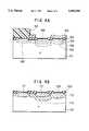
- FIGS. 1A to 2Bare cross-sectional views showing the steps of a conventional method of fabricating a semiconductor having a retrograde-distributed triple well structure.
- field oxide layers 202having a thickness of 400 nm, by means of the LOCOS process.
- silicon oxide layers 203having a thickness of 50 nm, by means of the thermal oxidation process.
- photoresist layers 204having openings on a region on which buried n-well layers are to be formed.
- buried ion implantation layers 205are formed by implanting phosphorus by the number of 1 ⁇ 10 13 per square centimeter at an energy of, for instance, 2 MeV with the photoresist layers 204 acting as a mask.
- first ion implantation layers 207are formed by implanting boron by the number of 4 ⁇ 10 12 per square centimeter at an energy of 140 KeV with the photoresist layers 206 acting as a mask, and subsequently there are formed second ion implantation layers 208 by implanting boron by the number of 2 ⁇ 10 13 per square centimeter at an energy of 400 KeV.
- the first ion implantation layers 207act as a channel stopping layer present under the field oxide layers in the p-well regions, and the second ion implantation layers 208 act to form a main body of the p-well layers.
- third ion implantation layers 210are formed by implanting phosphorus by the number of 4 ⁇ 10 12 per square centimeter at an energy of 400 KeV with the photoresist layers 209 acting as a mask, and subsequently there are formed fourth ion implantation layers 211 by implanting phosphorus by the number of 2 ⁇ 10 13 per square centimeter at an energy of 1 MeV.
- the third ion implantation layers 210act as a channel stopping layer present under the field oxide layers in the n-well regions, and the fourth ion implantation layers 211 act to form a main body of the n-well layers.
- impurities implanted into the buried ion implantation layers 205, the first ion implantation layers 207, the second ion implantation layers 208, the third ion implantation layers 210 and the fourth ion implantation layers 211are activated by thermal treatment carried out, for instance, at 1000 degrees centigrade for 30 minutes.
- thermal treatmentcarried out, for instance, at 1000 degrees centigrade for 30 minutes.
- the conventional method of forming retrograde-distributed triple wellthere are required three masks for photolithography: one for forming the buried n-well layers 214, one for forming the p-well layers 211 and one for forming n-well layers 213.
- the methodrequires five ion-implantations: one for forming the buried ion implantation layers 205, one for forming the first ion implantation layers 207, one for forming the second ion implantation layers 208, one for forming the third ion implantation layers 210 and one for forming the fourth ion implantation layers 211.
- the conventional methodposes a problem that the large number of masks are necessary for forming a triple well structure, and hence the steps for fabricating a semiconductor device have to be complicated.
- the inventionprovides a method of fabricating a semiconductor device, including the steps of: forming a plurality of active regions on a semiconductor substrate; covering a first active region with mask layers including a first mask layer and a second mask layer deposited on the first mask layer; implanting first electrically conductive type impurities into a second active region with the mask layers acting as a mask; removing the second mask layer; and implanting second electrically conductive type impurities into the first and second active regions.
- the inventionalso provides a method of fabricating a semiconductor device, including the steps of: forming a plurality of active regions on a semiconductor substrate; covering a first active region with mask layers including a first mask layer and a second mask layer deposited on the first mask layer; implanting first electrically conductive type impurities into second and third active regions with the mask layers acting as a mask; removing the second mask layer; covering the third active regions with a third mask layer; and implanting second electrically conductive type impurities into the first and second active regions.
- the semiconductor substrateis of a first electrically conductive type.
- the first mask layeris composed of poly silicon and the second mask layer is composed of photoresist.
- the step of implanting first electrically conductive type impurities and/or the step of implanting second electrically conductive type impuritiesare(is) achieved by a plurality of ion-implantations having different ranges.
- the methodfurther includes the step of ion-implanting for adjusting a threshold voltage of a MOS type transistor. This step is to be carried out just before the step of covering the first active region with the mask layers.
- the methodfurther includes the step of ion-implanting for adjusting a threshold voltage of a MOS transistor. This step is to be carried out just before the step of implanting first electrically conductive type impurities into the second active region with the mask layers acting as a mask.
- the methodfurther includes the step of ion-implanting for adjusting a threshold voltage of a MOS transistor. This step is to be carried out just before the step of implanting second electrically conductive type impurities into the first and second active regions.
- the methodfurther includes the step of covering a region located between the second and third active regions with the same mask layers as the mask layers with which the first active region is covered.
- the step of covering a region located between the second and third active regions with the same mask layers as the mask layers with which the first active region is coveredis concurrently carried out with the step of covering the first active region with the mask layers.
- the plurality of active regionsare formed by oxidizing the semiconductor substrate at selected regions.
- one of main surfaces of a semiconductor substrateis oxidized at selected regions to thereby define active regions and non-active regions.
- stacked mask layerscomprising a first mask layer and a second mask layer deposited on the first mask layer is formed on the semiconductor substrate in a desired pattern.
- first electrically conductive type impuritiesare selectively ion-implanted.
- second electrically conductive type impuritiesare ion-implanted with at least a part of the first mask layer remaining present on the semiconductor substrate.
- a retrograde-distributed triple well structurecan be formed with less number of masks and less number of ion implantations than conventional methods.
- FIGS. 1A, 1B, 2A and 2Bare cross-sectional views showing the steps of a conventional method of fabricating a semiconductor device having a retrograde-distributed triple well structure.
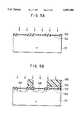
- FIGS. 3A, 3B, 4A and 4Bare cross-sectional views showing the steps of a method in accordance with a first embodiment of the present invention.
- FIGS. 5A, 5B, 6A and 6Bare cross-sectional views showing the steps of a method in accordance with a second embodiment of the present invention.
- field oxide layers 102having a thickness of 400 nm by means of LOCOS process on one of main surfaces of a p-type silicon substrate 101.
- silicon dioxide layers 103having a thickness of 50 nm by means of thermal oxidation process on a region in which the field oxide layers 102 are not formed.
- a poly crystalline silicon layer 104which is to act as a mask and have a thickness of 800 nm are formed by means of LPCVD (low-pressure chemical vapor deposition) process.
- LPCVDlow-pressure chemical vapor deposition
- the photoresist layer 105is removed only at regions where p-well layers are to be formed.
- the poly crystalline silicon layer 104are patterned by reactive ion etching using the photoresist layer 105 as a mask to thereby have the same pattern as the photoresist layer 105.
- first ion implantation layers 106by implanting boron by the number of 4 ⁇ 10 12 per square centimeter at an energy of 140 KeV
- second ion implantation layers 107by implanting boron by the number of 5 ⁇ 10 13 per square centimeter at an energy of 400 KeV with the stacked layers 104 and 105 acting as a mask.
- the first ion implantation layer 106is formed for forming a channel stopper in a p-well layer to be formed below the field oxidation layer 102, and also for forming a layer in a p-well layer in active regions, which layer is for preventing punch-through between a source and a drain of a transistor.
- the second ion implantation layer 107is formed for forming a main body of a p-well layer.
- a photoresist layer 310having a thickness of 4 ⁇ m with the poly crystalline silicon layer 104 acting as a mask remaining as they are.
- a region where a n-well layer 112 and an buried n-well layer 113 are to be formedis exposed.
- a third ion implantation layer 108by implanting phosphorus by the number of 5 ⁇ 10 12 per square centimeter at an energy of 1.2 MeV
- a fourth ion implantation layer 109by implanting phosphorus by the number of 3 ⁇ 10 13 per square centimeter at an energy of 2 MeV.
- the third and fourth ion implantation layers 108 and 109phosphorus does not reach the p-type silicon substrate 101 in a region where the photoresist layer 110 is still existent.
- the concentration of the third ion implantation layers 108 just below the field oxide layers 102there is a peak of the concentration of the fourth ion implantation layers 109 at a depth of approximately 0.9 ⁇ m from a surface of the p-type silicon substrate 101.
- a peak of the concentration of the third ion implantation 108is located at a depth of approximately 1.2 ⁇ m from a surface of the p-type silicon substrate 101, and a peak of the concentration of the fourth ion implantation 109 is located at a depth of approximately 1.8 ⁇ m from a surface of the p-type silicon substrate 101.
- the photoresist layers 110have been removed, the poly crystalline silicon layers 104 acting as a mask are also removed. Then, the substrate 101 is thermally treated at a temperature of 950 degrees centigrade for 30 minutes, to thereby electrically activate implanted impurities. Thus, there are formed retrograde-distributed p-well layers 111, n-well layers 112 and buried n-well layers 113.
- the third ion implantation layers 108in a region below the field oxide layers 102, act as a channel stopper having a concentration peak just below the field oxide layers 102, and in active regions where poly crystalline silicon layers 104 are formed, act as a punch-through preventing layer for preventing punch-through between a source and a drain of a transistor.
- the fourth ion implantation layers 109which have a concentration peak at a depth of 0.9 ⁇ m in a region where the poly crystalline silicon layer or mask 104 are still existent on the field oxide layers 102, becomes a main part of the n-well layers 112 in the active regions where the poly crystalline silicon layers 104 are still existent.
- the third ion implantation layers 108having a concentration peak located deeper than 1 ⁇ m from a surface of the substrate 101, and the fourth ion implantation layers 109 become the buried n-well layers 113.
- the embodimentmakes it possible to fabricate a semiconductor device having a retrograde-distributed triple well structure with two photolithography steps and four ion implantation steps.
- the embodimentprovides an advantage that masks and steps necessary for forming a retrograde-distributed triple well structure can be reduced. Specifically, the number of masks can be reduced from three (conventional method) to two (the invention), and the steps can be reduced from five (conventional method) to four (the invention).
- field oxide layers 102having a thickness of 400 nm by means of LOCOS process on one of main surfaces of a p-type silicon substrate 101.
- silicon dioxide layers 103having a thickness of 50 nm by means of thermal oxidation process on a region in which the field oxide layers 102 are not formed.
- a determined amount of boronis ion-implanted at an energy of 30 KeV.
- a poly crystalline silicon layer 104which is to act as a mask and have a thickness of 800 nm are formed by means of LPCVD (low-pressure chemical vapor deposition) process.
- LPCVDlow-pressure chemical vapor deposition
- the photoresist layer 105is removed only at regions where p-well layers are to be formed.
- the poly crystalline silicon layer 104are patterned by reactive ion etching using the photoresist layer 105 as a mask to thereby have the same pattern as the photoresist layer 105.
- first ion implantation layers 106by implanting boron by the number of 4 ⁇ 10 12 /cm 2 at an energy of 140 KeV
- second ion implantation layers 107by implanting boron by the number of 5 ⁇ 10 13 /cm 2 at an energy of 400 KeV with the stacked layers 104 and 105 acting as a mask.
- a determined amount of boronis ion-implanted at an energy of 30 KeV.
- a photoresist layer 110having a thickness of 4 ⁇ m with the poly crystalline silicon layer 104 acting as a mask remaining as they are.
- a region where a n-well layer 112 and a buried n-well layer 113 are to be formedis exposed.
- a third ion implantation layer 108by implanting phosphorus by the number of 5 ⁇ 10 12 per square centimeter at an energy of 1.2 MeV
- a fourth ion implantation layer 109by implanting phosphorus by the number of 3 ⁇ 10 13 per square centimeter at an energy of 2 MeV.
- a determined amount of boronis ion-implanted at an energy of 30 KeV.
- the photoresist layers 110have been removed, the poly crystalline silicon layers 104 acting as a mask are also removed. Then, the substrate 101 is thermally treated at a temperature of 950 degrees centigrade for 30 minutes, to thereby electrically activate implanted impurities. Thus, there are formed retrograde-distributed p-well layers 111, n-well layers 112 and buried n-well layers 113.
- gate oxidation layers 114After the silicon dioxide layers 103 have been removed, there are formed by means of a conventional method gate oxidation layers 114, gate electrodes 115, n+ type diffusion layers 116 and p+ type diffusion layers 117.
- the second embodimentprovides an advantage as well as that provided by the first embodiment, that it is possible by using a common mask to control a threshold voltage (Vth) of both a n-type surface channel transistor to be formed in the p-well layer 111 and a p-type buried channel transistor to be formed in the n-well layer 112.
- Vththreshold voltage
- the mask layersmay be composed of inorganic substances such as silicon nitride and organic substances such as polyimide in place of poly crystalline silicon.
- An energy for ion-implantation and dosagemay be varied as required.
Landscapes
- Engineering & Computer Science (AREA)
- Physics & Mathematics (AREA)
- Condensed Matter Physics & Semiconductors (AREA)
- General Physics & Mathematics (AREA)
- Manufacturing & Machinery (AREA)
- Computer Hardware Design (AREA)
- Microelectronics & Electronic Packaging (AREA)
- Power Engineering (AREA)
- Metal-Oxide And Bipolar Metal-Oxide Semiconductor Integrated Circuits (AREA)
Abstract
Description
Claims (8)
Applications Claiming Priority (2)
| Application Number | Priority Date | Filing Date | Title |
|---|---|---|---|
| JP5-347354 | 1993-12-24 | ||
| JP5347354AJP2682425B2 (en) | 1993-12-24 | 1993-12-24 | Method for manufacturing semiconductor device |
Publications (1)
| Publication Number | Publication Date |
|---|---|
| US5693505Atrue US5693505A (en) | 1997-12-02 |
Family
ID=18389662
Family Applications (1)
| Application Number | Title | Priority Date | Filing Date |
|---|---|---|---|
| US08/355,905Expired - Fee RelatedUS5693505A (en) | 1993-12-24 | 1994-12-14 | Method of fabricating a semiconductor device |
Country Status (2)
| Country | Link |
|---|---|
| US (1) | US5693505A (en) |
| JP (1) | JP2682425B2 (en) |
Cited By (24)
| Publication number | Priority date | Publication date | Assignee | Title |
|---|---|---|---|---|
| GB2320812A (en)* | 1996-12-30 | 1998-07-01 | Hyundai Electronics Ind | Method for forming a triple well of a semiconductor device |
| US5795803A (en)* | 1996-08-29 | 1998-08-18 | Sharp Kabushiki Kaisha | Method for manufacturing a semiconductor device |
| EP0793858A4 (en)* | 1994-11-22 | 1998-08-19 | Genus Inc | CONSTRUCTING CMOS VERTICALLY MODULATED WELLS BY CLUSTERED MeV BURIED IMPLANTED LAYER FOR LATERAL ISOLATION |
| US5927991A (en)* | 1995-12-30 | 1999-07-27 | Lg Semicon Co., Ltd. | Method for forming triple well in semiconductor device |
| US5963799A (en)* | 1998-03-23 | 1999-10-05 | Texas Instruments - Acer Incorporated | Blanket well counter doping process for high speed/low power MOSFETs |
| US5963801A (en)* | 1996-12-19 | 1999-10-05 | Lsi Logic Corporation | Method of forming retrograde well structures and punch-through barriers using low energy implants |
| US5966599A (en)* | 1996-05-21 | 1999-10-12 | Lsi Logic Corporation | Method for fabricating a low trigger voltage silicon controlled rectifier and thick field device |
| US5981327A (en)* | 1997-04-10 | 1999-11-09 | Lg Semicon Co., Ltd. | Method for forming wells of semiconductor device |
| US6017799A (en)* | 1997-12-20 | 2000-01-25 | United Microelectronics Corp. | Method of fabricating dynamic random memory |
| US6066523A (en)* | 1997-06-30 | 2000-05-23 | Hyundai Electronics Industries Co., Ltd. | Method for fabricating a semiconductor device having triple wells |
| US6133081A (en)* | 1998-05-07 | 2000-10-17 | Lg Semicon Co., Ltd. | Method of forming twin well |
| US6211003B1 (en)* | 1998-03-16 | 2001-04-03 | Hitachi, Ltd. | Semiconductor integrated circuit device and process for manufacturing the same |
| US6251744B1 (en) | 1999-07-19 | 2001-06-26 | Taiwan Semiconductor Manufacturing Company | Implant method to improve characteristics of high voltage isolation and high voltage breakdown |
| US6297119B1 (en)* | 1998-08-07 | 2001-10-02 | Nec Corporation | Semiconductor device and its manufacture |
| US6309921B1 (en)* | 1994-09-22 | 2001-10-30 | Fujitsu Limited | Semiconductor device and method for fabricating semiconductor device |
| US6312997B1 (en) | 1998-08-12 | 2001-11-06 | Micron Technology, Inc. | Low voltage high performance semiconductor devices and methods |
| US6372568B1 (en)* | 1997-11-28 | 2002-04-16 | Infineon Technologies Ag | Method of manufacture of a semiconductor having a triple well structure |
| US6461921B1 (en)* | 1997-02-27 | 2002-10-08 | Kabushiki Kaisha Toshiba | Semiconductor device having channel stopper portions integrally formed as part of a well |
| US6514810B1 (en)* | 2001-08-01 | 2003-02-04 | Texas Instruments Incorporated | Buried channel PMOS transistor in dual gate CMOS with reduced masking steps |
| US6514807B1 (en)* | 2001-09-18 | 2003-02-04 | Macronix International Co., Ltd. | Method for fabricating semiconductor device applied system on chip |
| US6531363B2 (en) | 1998-03-05 | 2003-03-11 | Nec Corporation | Method for manufacturing a semiconductor integrated circuit of triple well structure |
| US20030232490A1 (en)* | 2002-03-07 | 2003-12-18 | Masahiro Hayashi | Method for manufacturing semiconductor device |
| US20050014329A1 (en)* | 2002-08-14 | 2005-01-20 | Advanced Analogic Technologies, Inc. | Method of fabricating isolated semiconductor devices in epi-less substrate |
| CN1306615C (en)* | 1996-08-26 | 2007-03-21 | 三菱电机株式会社 | Semiconductor device and method of manufacturing the same |
Families Citing this family (7)
| Publication number | Priority date | Publication date | Assignee | Title |
|---|---|---|---|---|
| KR100283712B1 (en) | 1996-06-24 | 2001-04-02 | 모리시타 요이찌 | Manufacturing Method of Semiconductor Device |
| TW434834B (en)* | 1996-06-29 | 2001-05-16 | Hyundai Electronics Ind | Method of manufacturing a complementary metal-oxide semiconductor device |
| JP3777000B2 (en)* | 1996-12-20 | 2006-05-24 | 富士通株式会社 | Semiconductor device and manufacturing method thereof |
| KR100474505B1 (en)* | 1997-12-23 | 2005-05-19 | 주식회사 하이닉스반도체 | Manufacturing method of semiconductor device |
| KR100265225B1 (en) | 1998-06-05 | 2000-09-15 | 김영환 | Method for fabricating semiconductor device |
| KR100483029B1 (en)* | 1998-06-29 | 2005-07-07 | 주식회사 하이닉스반도체 | Triple well manufacturing method of semiconductor device |
| KR100322889B1 (en)* | 1999-12-30 | 2002-02-09 | 박종섭 | Method for manufacturing a semiconductor device |
Citations (20)
| Publication number | Priority date | Publication date | Assignee | Title |
|---|---|---|---|---|
| US4717684A (en)* | 1985-02-01 | 1988-01-05 | Hitachi, Ltd. | Semiconductor integrated circuit device |
| US4753898A (en)* | 1987-07-09 | 1988-06-28 | Motorola, Inc. | LDD CMOS process |
| US4908327A (en)* | 1988-05-02 | 1990-03-13 | Texas Instruments, Incorporated | Counter-doped transistor |
| US4997782A (en)* | 1988-08-04 | 1991-03-05 | Sgs-Thomson Microelectronics S.R.L. | Fabrication of CMOS integrated devices with reduced gate length and lightly doped drain |
| US5091324A (en)* | 1990-08-10 | 1992-02-25 | Advanced Micro Devices, Inc. | Process for producing optimum intrinsic, long channel, and short channel mos devices in vlsi structures |
| US5238864A (en)* | 1990-12-21 | 1993-08-24 | Mitsubishi Denki Kabushiki Kaisha | Method of making solid-state imaging device |
| US5254487A (en)* | 1992-05-13 | 1993-10-19 | Nec Corporation | Method of manufacturing high and low voltage CMOS transistors on a single chip |
| US5278078A (en)* | 1991-05-14 | 1994-01-11 | Kabushiki Kaisha Toshiba | Method of manufacturing semiconductor device |
| US5290717A (en)* | 1990-04-27 | 1994-03-01 | Kawasaki Steel Corporation | Method of manufacturing semiconductor devices having a resist patern coincident with gate electrode |
| US5342802A (en)* | 1990-04-13 | 1994-08-30 | Nippondenso Co., Ltd. | Method of manufacturing a complementary MIS transistor |
| US5396096A (en)* | 1992-10-07 | 1995-03-07 | Matsushita Electric Industrial Co., Ltd. | Semiconductor device and manufacturing method thereof |
| US5403764A (en)* | 1992-04-28 | 1995-04-04 | Rohm Co., Ltd. | Method for producing a ROM on a semiconductor device having a nonvolatile memory |
| US5407849A (en)* | 1992-06-23 | 1995-04-18 | Imp, Inc. | CMOS process and circuit including zero threshold transistors |
| US5432114A (en)* | 1994-10-24 | 1995-07-11 | Analog Devices, Inc. | Process for integration of gate dielectric layers having different parameters in an IGFET integrated circuit |
| US5439835A (en)* | 1993-11-12 | 1995-08-08 | Micron Semiconductor, Inc. | Process for DRAM incorporating a high-energy, oblique P-type implant for both field isolation and punchthrough |
| US5460984A (en)* | 1989-09-11 | 1995-10-24 | Kabushiki Kaisha Toshiba | Method of manufacturing a semi conductor device having a second well formed within a first well |
| US5478761A (en)* | 1989-11-24 | 1995-12-26 | Mitsubishi Denki Kabushiki Kaisha | Method of producing semiconductor device having first and second type field effect transistors |
| US5498553A (en)* | 1993-11-01 | 1996-03-12 | United Microelectronics Corporation | Method of making a metal gate high voltage integrated circuit |
| US5501993A (en)* | 1994-11-22 | 1996-03-26 | Genus, Inc. | Method of constructing CMOS vertically modulated wells (VMW) by clustered MeV BILLI (buried implanted layer for lateral isolation) implantation |
| US5534448A (en)* | 1993-07-29 | 1996-07-09 | Sgs-Thomson Microelectronics S.R.L. | Process for realizing P-channel MOS transistors having a low threshold voltage in semiconductor integrated circuits for analog applications |
Family Cites Families (1)
| Publication number | Priority date | Publication date | Assignee | Title |
|---|---|---|---|---|
| JPH0492466A (en)* | 1990-08-07 | 1992-03-25 | Mitsubishi Electric Corp | Semiconductor device and manufacture thereof |
- 1993
- 1993-12-24JPJP5347354Apatent/JP2682425B2/ennot_activeExpired - Fee Related
- 1994
- 1994-12-14USUS08/355,905patent/US5693505A/ennot_activeExpired - Fee Related
Patent Citations (20)
| Publication number | Priority date | Publication date | Assignee | Title |
|---|---|---|---|---|
| US4717684A (en)* | 1985-02-01 | 1988-01-05 | Hitachi, Ltd. | Semiconductor integrated circuit device |
| US4753898A (en)* | 1987-07-09 | 1988-06-28 | Motorola, Inc. | LDD CMOS process |
| US4908327A (en)* | 1988-05-02 | 1990-03-13 | Texas Instruments, Incorporated | Counter-doped transistor |
| US4997782A (en)* | 1988-08-04 | 1991-03-05 | Sgs-Thomson Microelectronics S.R.L. | Fabrication of CMOS integrated devices with reduced gate length and lightly doped drain |
| US5460984A (en)* | 1989-09-11 | 1995-10-24 | Kabushiki Kaisha Toshiba | Method of manufacturing a semi conductor device having a second well formed within a first well |
| US5478761A (en)* | 1989-11-24 | 1995-12-26 | Mitsubishi Denki Kabushiki Kaisha | Method of producing semiconductor device having first and second type field effect transistors |
| US5342802A (en)* | 1990-04-13 | 1994-08-30 | Nippondenso Co., Ltd. | Method of manufacturing a complementary MIS transistor |
| US5290717A (en)* | 1990-04-27 | 1994-03-01 | Kawasaki Steel Corporation | Method of manufacturing semiconductor devices having a resist patern coincident with gate electrode |
| US5091324A (en)* | 1990-08-10 | 1992-02-25 | Advanced Micro Devices, Inc. | Process for producing optimum intrinsic, long channel, and short channel mos devices in vlsi structures |
| US5238864A (en)* | 1990-12-21 | 1993-08-24 | Mitsubishi Denki Kabushiki Kaisha | Method of making solid-state imaging device |
| US5278078A (en)* | 1991-05-14 | 1994-01-11 | Kabushiki Kaisha Toshiba | Method of manufacturing semiconductor device |
| US5403764A (en)* | 1992-04-28 | 1995-04-04 | Rohm Co., Ltd. | Method for producing a ROM on a semiconductor device having a nonvolatile memory |
| US5254487A (en)* | 1992-05-13 | 1993-10-19 | Nec Corporation | Method of manufacturing high and low voltage CMOS transistors on a single chip |
| US5407849A (en)* | 1992-06-23 | 1995-04-18 | Imp, Inc. | CMOS process and circuit including zero threshold transistors |
| US5396096A (en)* | 1992-10-07 | 1995-03-07 | Matsushita Electric Industrial Co., Ltd. | Semiconductor device and manufacturing method thereof |
| US5534448A (en)* | 1993-07-29 | 1996-07-09 | Sgs-Thomson Microelectronics S.R.L. | Process for realizing P-channel MOS transistors having a low threshold voltage in semiconductor integrated circuits for analog applications |
| US5498553A (en)* | 1993-11-01 | 1996-03-12 | United Microelectronics Corporation | Method of making a metal gate high voltage integrated circuit |
| US5439835A (en)* | 1993-11-12 | 1995-08-08 | Micron Semiconductor, Inc. | Process for DRAM incorporating a high-energy, oblique P-type implant for both field isolation and punchthrough |
| US5432114A (en)* | 1994-10-24 | 1995-07-11 | Analog Devices, Inc. | Process for integration of gate dielectric layers having different parameters in an IGFET integrated circuit |
| US5501993A (en)* | 1994-11-22 | 1996-03-26 | Genus, Inc. | Method of constructing CMOS vertically modulated wells (VMW) by clustered MeV BILLI (buried implanted layer for lateral isolation) implantation |
Cited By (45)
| Publication number | Priority date | Publication date | Assignee | Title |
|---|---|---|---|---|
| US6309921B1 (en)* | 1994-09-22 | 2001-10-30 | Fujitsu Limited | Semiconductor device and method for fabricating semiconductor device |
| EP0793858A4 (en)* | 1994-11-22 | 1998-08-19 | Genus Inc | CONSTRUCTING CMOS VERTICALLY MODULATED WELLS BY CLUSTERED MeV BURIED IMPLANTED LAYER FOR LATERAL ISOLATION |
| US5927991A (en)* | 1995-12-30 | 1999-07-27 | Lg Semicon Co., Ltd. | Method for forming triple well in semiconductor device |
| US5966599A (en)* | 1996-05-21 | 1999-10-12 | Lsi Logic Corporation | Method for fabricating a low trigger voltage silicon controlled rectifier and thick field device |
| CN1306615C (en)* | 1996-08-26 | 2007-03-21 | 三菱电机株式会社 | Semiconductor device and method of manufacturing the same |
| US5795803A (en)* | 1996-08-29 | 1998-08-18 | Sharp Kabushiki Kaisha | Method for manufacturing a semiconductor device |
| US5963801A (en)* | 1996-12-19 | 1999-10-05 | Lsi Logic Corporation | Method of forming retrograde well structures and punch-through barriers using low energy implants |
| US6010926A (en)* | 1996-12-30 | 2000-01-04 | Hyundai Electronics Industries Co., Ltd. | Method for forming multiple or modulated wells of semiconductor device |
| GB2320812A (en)* | 1996-12-30 | 1998-07-01 | Hyundai Electronics Ind | Method for forming a triple well of a semiconductor device |
| GB2320812B (en)* | 1996-12-30 | 2002-01-09 | Hyundai Electronics Ind | Method for forming a triple well of a semiconductor device |
| US6461921B1 (en)* | 1997-02-27 | 2002-10-08 | Kabushiki Kaisha Toshiba | Semiconductor device having channel stopper portions integrally formed as part of a well |
| US5981327A (en)* | 1997-04-10 | 1999-11-09 | Lg Semicon Co., Ltd. | Method for forming wells of semiconductor device |
| US6066523A (en)* | 1997-06-30 | 2000-05-23 | Hyundai Electronics Industries Co., Ltd. | Method for fabricating a semiconductor device having triple wells |
| US6372568B1 (en)* | 1997-11-28 | 2002-04-16 | Infineon Technologies Ag | Method of manufacture of a semiconductor having a triple well structure |
| US6017799A (en)* | 1997-12-20 | 2000-01-25 | United Microelectronics Corp. | Method of fabricating dynamic random memory |
| US6531363B2 (en) | 1998-03-05 | 2003-03-11 | Nec Corporation | Method for manufacturing a semiconductor integrated circuit of triple well structure |
| US6387744B2 (en) | 1998-03-16 | 2002-05-14 | Hitachi, Ltd. | Process for manufacturing semiconductor integrated circuit device |
| US6211003B1 (en)* | 1998-03-16 | 2001-04-03 | Hitachi, Ltd. | Semiconductor integrated circuit device and process for manufacturing the same |
| US5963799A (en)* | 1998-03-23 | 1999-10-05 | Texas Instruments - Acer Incorporated | Blanket well counter doping process for high speed/low power MOSFETs |
| US6133081A (en)* | 1998-05-07 | 2000-10-17 | Lg Semicon Co., Ltd. | Method of forming twin well |
| US6297119B1 (en)* | 1998-08-07 | 2001-10-02 | Nec Corporation | Semiconductor device and its manufacture |
| US20040198004A1 (en)* | 1998-08-12 | 2004-10-07 | Tran Luan C | Low voltage high performance semiconductor devices and methods |
| US6492693B2 (en) | 1998-08-12 | 2002-12-10 | Micron Technology, Inc. | Low voltage high performance semiconductor devices and methods |
| US6312997B1 (en) | 1998-08-12 | 2001-11-06 | Micron Technology, Inc. | Low voltage high performance semiconductor devices and methods |
| US6946353B2 (en) | 1998-08-12 | 2005-09-20 | Micron Technology, Inc. | Low voltage high performance semiconductor devices and methods |
| US6747326B2 (en) | 1998-08-12 | 2004-06-08 | Micron Technology, Inc. | Low voltage high performance semiconductor device having punch through prevention implants |
| US6251744B1 (en) | 1999-07-19 | 2001-06-26 | Taiwan Semiconductor Manufacturing Company | Implant method to improve characteristics of high voltage isolation and high voltage breakdown |
| US6514810B1 (en)* | 2001-08-01 | 2003-02-04 | Texas Instruments Incorporated | Buried channel PMOS transistor in dual gate CMOS with reduced masking steps |
| US6514807B1 (en)* | 2001-09-18 | 2003-02-04 | Macronix International Co., Ltd. | Method for fabricating semiconductor device applied system on chip |
| US6929994B2 (en)* | 2002-03-07 | 2005-08-16 | Seiko Epson Corporation | Method for manufacturing semiconductor device that includes well formation |
| US20030232490A1 (en)* | 2002-03-07 | 2003-12-18 | Masahiro Hayashi | Method for manufacturing semiconductor device |
| US20060223257A1 (en)* | 2002-08-14 | 2006-10-05 | Advanced Analogic Technologies, Inc. | Method Of Fabricating Isolated Semiconductor Devices In Epi-Less Substrate |
| US7276431B2 (en) | 2002-08-14 | 2007-10-02 | Advanced Analogic Technologies, Inc. | Method of fabricating isolated semiconductor devices in epi-less substrate |
| US20050158939A1 (en)* | 2002-08-14 | 2005-07-21 | Advanced Analogic Technologies, Inc | Method of fabricating isolated semiconductor devices in epi-less substrate |
| US20050142791A1 (en)* | 2002-08-14 | 2005-06-30 | Advanced Analogic Technologies, Inc. | Method of fabricating isolated semiconductor devices in epi-less substrate |
| US20050142792A1 (en)* | 2002-08-14 | 2005-06-30 | Advanced Analogic Technologies, Inc. | Method of fabricating isolated semiconductor devices in epi-less substrate |
| US20050014329A1 (en)* | 2002-08-14 | 2005-01-20 | Advanced Analogic Technologies, Inc. | Method of fabricating isolated semiconductor devices in epi-less substrate |
| US20050014324A1 (en)* | 2002-08-14 | 2005-01-20 | Advanced Analogic Technologies, Inc. | Method of fabricating isolated semiconductor devices in epi-less substrate |
| US20050142724A1 (en)* | 2002-08-14 | 2005-06-30 | Advanced Analogic Technologies, Inc. | Method of fabricating isolated semiconductor devices in epi-less substrate |
| US7279378B2 (en)* | 2002-08-14 | 2007-10-09 | Advanced Analogic Technologies, Inc. | Method of fabricating isolated semiconductor devices in epi-less substrate |
| US7329583B2 (en)* | 2002-08-14 | 2008-02-12 | Advanced Analogic Technologies, Inc. | Method of fabricating isolated semiconductor devices in epi-less substrate |
| US7422938B2 (en) | 2002-08-14 | 2008-09-09 | Advanced Analogic Technologies, Inc. | Method of fabricating isolated semiconductor devices in epi-less substrate |
| US7445979B2 (en) | 2002-08-14 | 2008-11-04 | Advanced Analogic Technologies, Inc. | Method of fabricating isolated semiconductor devices in epi-less substrate |
| US7449380B2 (en) | 2002-08-14 | 2008-11-11 | Advanced Analogic Technologies, Inc. | Method of fabricating isolated semiconductor devices in epi-less substrate |
| US7666756B2 (en)* | 2002-08-14 | 2010-02-23 | Advanced Analogic Technologies, Inc. | Methods of fabricating isolation structures in epi-less substrate |
Also Published As
| Publication number | Publication date |
|---|---|
| JP2682425B2 (en) | 1997-11-26 |
| JPH07183393A (en) | 1995-07-21 |
Similar Documents
| Publication | Publication Date | Title |
|---|---|---|
| US5693505A (en) | Method of fabricating a semiconductor device | |
| US5683927A (en) | Method of forming CMOS integrated circuitry | |
| US4717683A (en) | CMOS process | |
| US5024965A (en) | Manufacturing high speed low leakage radiation hardened CMOS/SOI devices | |
| KR100265227B1 (en) | Method for fabricating cmos transistor | |
| US4435895A (en) | Process for forming complementary integrated circuit devices | |
| US6309921B1 (en) | Semiconductor device and method for fabricating semiconductor device | |
| US6004854A (en) | Method of forming CMOS integrated circuitry | |
| JPH0576190B2 (en) | ||
| JPH1074844A (en) | Method for manufacturing semiconductor device | |
| JPH04255266A (en) | Improved method for formation of mos transistor as vlsi structure on semiconductor wafer | |
| US4931407A (en) | Method for manufacturing integrated bipolar and MOS transistors | |
| US5936287A (en) | Nitrogenated gate structure for improved transistor performance and method for making same | |
| US4462151A (en) | Method of making high density complementary transistors | |
| KR100324931B1 (en) | Method of Fabricating a Twin Well CMOS Device | |
| US6647542B2 (en) | Efficient fabrication process for dual well type structures | |
| US4481705A (en) | Process for doping field isolation regions in CMOS integrated circuits | |
| KR980006254A (en) | Method of manufacturing semiconductor device | |
| KR100312808B1 (en) | Method of fabricating dual voltage mos transistors | |
| JPS61236154A (en) | Semiconductor device | |
| JP2550691B2 (en) | Method for manufacturing semiconductor device | |
| JP2003068876A (en) | Semiconductor device and manufacturing method thereof | |
| JPH063808B2 (en) | Method for manufacturing MOS semiconductor device | |
| JP3168676B2 (en) | Complementary MIS transistor device and method of manufacturing the same | |
| JP3057692B2 (en) | Method for manufacturing semiconductor device |
Legal Events
| Date | Code | Title | Description |
|---|---|---|---|
| AS | Assignment | Owner name:NEC CORPORATION, JAPAN Free format text:ASSIGNMENT OF ASSIGNORS INTEREST;ASSIGNOR:KOBAYASHI, MIGAKU;REEL/FRAME:007269/0343 Effective date:19941207 | |
| FEPP | Fee payment procedure | Free format text:PAYOR NUMBER ASSIGNED (ORIGINAL EVENT CODE: ASPN); ENTITY STATUS OF PATENT OWNER: LARGE ENTITY | |
| FPAY | Fee payment | Year of fee payment:4 | |
| AS | Assignment | Owner name:NEC ELECTRONICS CORPORATION, JAPAN Free format text:ASSIGNMENT OF ASSIGNORS INTEREST;ASSIGNOR:NEC CORPORATION;REEL/FRAME:013758/0595 Effective date:20030110 | |
| AS | Assignment | Owner name:ELPIDA MEMORY, INC., JAPAN Free format text:ASSIGNMENT OF ASSIGNORS INTEREST;ASSIGNORS:NEC CORPORATION;NEC ELECTRONICS CORPORATION;REEL/FRAME:014981/0119 Effective date:20040426 | |
| FPAY | Fee payment | Year of fee payment:8 | |
| REMI | Maintenance fee reminder mailed | ||
| LAPS | Lapse for failure to pay maintenance fees | ||
| STCH | Information on status: patent discontinuation | Free format text:PATENT EXPIRED DUE TO NONPAYMENT OF MAINTENANCE FEES UNDER 37 CFR 1.362 | |
| FP | Lapsed due to failure to pay maintenance fee | Effective date:20091202 |