US5691945A - Technique for reconfiguring a high density memory - Google Patents
Technique for reconfiguring a high density memoryDownload PDFInfo
- Publication number
- US5691945A US5691945AUS08/605,100US60510096AUS5691945AUS 5691945 AUS5691945 AUS 5691945AUS 60510096 AUS60510096 AUS 60510096AUS 5691945 AUS5691945 AUS 5691945A
- Authority
- US
- United States
- Prior art keywords
- sectors
- array
- address
- sector
- subset
- Prior art date
- Legal status (The legal status is an assumption and is not a legal conclusion. Google has not performed a legal analysis and makes no representation as to the accuracy of the status listed.)
- Expired - Lifetime
Links
- 230000015654memoryEffects0.000titleclaimsabstractdescription70
- 238000000034methodMethods0.000titleclaimsabstractdescription31
- 230000002950deficientEffects0.000claimsabstractdescription63
- 238000000638solvent extractionMethods0.000claimsabstractdescription19
- 230000004044responseEffects0.000claimsabstractdescription9
- 238000007667floatingMethods0.000claimsdescription10
- 230000008569processEffects0.000claimsdescription8
- 238000004519manufacturing processMethods0.000abstractdescription16
- 210000004027cellAnatomy0.000description33
- 238000009792diffusion processMethods0.000description16
- 239000000872bufferSubstances0.000description11
- 239000002184metalSubstances0.000description10
- 238000010586diagramMethods0.000description5
- 238000013459approachMethods0.000description4
- 101100202463Schizophyllum commune SC14 geneProteins0.000description3
- 230000007547defectEffects0.000description2
- 238000013461designMethods0.000description2
- 238000005516engineering processMethods0.000description2
- 238000002955isolationMethods0.000description2
- 238000010420art techniqueMethods0.000description1
- 230000001143conditioned effectEffects0.000description1
- PWPJGUXAGUPAHP-UHFFFAOYSA-NlufenuronChemical compoundC1=C(Cl)C(OC(F)(F)C(C(F)(F)F)F)=CC(Cl)=C1NC(=O)NC(=O)C1=C(F)C=CC=C1FPWPJGUXAGUPAHP-UHFFFAOYSA-N0.000description1
- 238000013507mappingMethods0.000description1
- 238000012986modificationMethods0.000description1
- 230000004048modificationEffects0.000description1
- 238000011084recoveryMethods0.000description1
- 238000012552reviewMethods0.000description1
- 230000011218segmentationEffects0.000description1
- 239000004065semiconductorSubstances0.000description1
- 210000000352storage cellAnatomy0.000description1
- 238000012360testing methodMethods0.000description1
- 230000007704transitionEffects0.000description1
- 239000002699waste materialSubstances0.000description1
Images


Classifications
- G—PHYSICS
- G11—INFORMATION STORAGE
- G11C—STATIC STORES
- G11C29/00—Checking stores for correct operation ; Subsequent repair; Testing stores during standby or offline operation
- G11C29/70—Masking faults in memories by using spares or by reconfiguring
- G11C29/76—Masking faults in memories by using spares or by reconfiguring using address translation or modifications
- G—PHYSICS
- G11—INFORMATION STORAGE
- G11C—STATIC STORES
- G11C8/00—Arrangements for selecting an address in a digital store
- G11C8/08—Word line control circuits, e.g. drivers, boosters, pull-up circuits, pull-down circuits, precharging circuits, for word lines
- G—PHYSICS
- G11—INFORMATION STORAGE
- G11C—STATIC STORES
- G11C8/00—Arrangements for selecting an address in a digital store
- G11C8/10—Decoders
- G—PHYSICS
- G11—INFORMATION STORAGE
- G11C—STATIC STORES
- G11C8/00—Arrangements for selecting an address in a digital store
- G11C8/12—Group selection circuits, e.g. for memory block selection, chip selection, array selection
Definitions
- the present inventionrelates to manufacturing of integrated circuit memory such as flash EEPROM and the like, and more particularly to techniques for improving the yield in manufacturing of high density memories.
- Integrated circuit manufacturersuse memory redundancy techniques to improve the yield in memory devices. That is, if a particular cell is detected bad, which resides along a particular row or column of the memory, a replacement column or a replacement row can be energized, and the address for the defective row or column redirected to the replacement row or column. This address redirecting preserves the sequential addressing of the data, while replacing a defective cell in the array. However, if there are more defective cells along a given row or column, than can be corrected using the redundancy built in the design, then the memory is bad and cannot be used.
- This prior art techniqueis limited in its application because it requires that no defective cells are found in at least one half of the array. If a defective cell occurs in each half, then device has to be discarded. To retain sequential addressing, this technique requires that only the highest order address bit be manipulated in this way. Otherwise, sophisticated manufacturing techniques which ensure that the address buffers are wired to particular pins on the chip package must be executed to match enabled address buffers with address bus lines.
- the techniqueshould be more flexible than the prior art, allowing for recovery and use of larger number of die in the manufacturing run.
- the present inventionprovides a flexible technique for improving yield of manufacturing of high density memory devices, such as flash EEPROM.
- the techniqueinvolves configuring an integrated circuit memory array into a plurality of sectors selected by a sector decoder. If defective sectors are detected in the array, it may be partitioned by disabling defective sectors by configuring the sector decoder to prevent access to the defective sectors, while maintaining sequential addressing for remaining sectors in the array.
- the step of partitioning according to a preferred implementationincludes configuring the sector decoder to replace a defective sector in the array identified by N address bits, by another sector in the array having N-m of the N address bits which identify a sector, in common with the defective sector.
- a defective sector in the first subsetis replaced by a good sector in a second subset having the other N-1 address bits in common with the defective sector. Therefore, the process supports a system in which defects are detected in both halves of the array. As long as a good sector in the bottom half which has the same N-1 bits as a bad sector in the top half can be found, then the top half of the device can be configured as a memory device with sequential addressing and one half the size of the original array.
- Configuring the device at the sector decoding level rather than at the address buffer level as described by the prior artprovides further advantages.
- sequential addressingcan be achieved with any defective sector removed by providing configuration logic of sufficient depth, without requiring that the wiring from address input buffer to a pin on the package be altered.
- the step of partitioningmay include preventing wordlines in disabled sectors from receiving the negative voltage.
- the step of partitioninginvolves providing a configuration store on the integrated circuit which is coupled to the sector level address decoder.
- the step of partitioningis accomplished by programming the configuration store.
- the present inventioncan be characterized as an integrated circuit memory, such as a high density 16 megabit or higher flash EEPROM, which comprises an array of memory cells including a plurality of sectors.
- a decoderresponsive to memory addresses is used for accessing memory cells in the plurality of sectors.
- Programmable circuitry coupled to the decoderis used for configuring the decoder so that a subset including one or more of the plurality of sectors is disabled and remaining sectors are accessed by sequential addresses.
- the plurality of sectorsare identified by an N bit field in a memory address.
- the programmable circuitryincludes logic which divides the array into a first subset including sectors having a particular m bit subfield of the N bits field at a first value, and a second subset including sectors having the particular m bit subfield of the N bit field different from the first value, and substitutes in the sequential addressing a defective sector in the first subset with a sector in the second subset having N-m bits of the N bit field in common with the defective sector.
- the first and second subsetseach include half the sectors in the array.
- very flexible partitioning of the arraycan be exercised to make devices that are not only one half the original size, but also for instance that are one quarter the size of the original array, or three quarters size of the original array.
- the present inventionis easy to implement, not requiring complex changes to address input/output structures or to the array itself.
- the present inventionprovides an effective practical technique for improving the yield of manufacturing of high density memory devices such as flash EEPROMS.
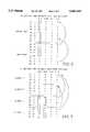
- FIG. 1is a schematic block diagram of a high density memory device with a plurality of sectors and a configuration store according to the present invention.
- FIGS. 2 and 3illustrate the logic of configuring memory according to respective embodiments of the present invention.
- FIG. 4is a circuit schematic diagram of a segmentable flash EEPROM array for use in the architecture of FIG. 1.
- FIG. 5is a schematic diagram of wordline driver used in a preferred embodiment of the system of FIG. 1, which supplies a negative voltage to wordlines in the array during programming.
- FIG. 6is a logic diagram for a pre-decoder for address bits A16-A18 for the system of FIG. 1.
- FIG. 7is the logic for address bit A19 in the pre-decoder in the system of FIG. 1.
- FIG. 8illustrates logic in the sector decoder for an upper half of the array.
- FIG. 9illustrates logic in the sector decoder for the lower half of the array.
- FIG. 10illustrates control logic used in conjunction with the sector decoder of FIG. 9.
- FIG. 11is a schematic illustration of the configuration store for use with the decoder of FIG. 9.
- FIG. 1illustrates an architecture of a device using the configurable sector decoder according to the present invention.
- the deviceincludes a high density memory array, generally 10, which includes a plurality of sectors: sector 0 through sector 15.
- the array 10is decoded vertically by a column decoder 11, and decoded horizontally by sector decoder 12 and by the wordline decoder and drivers 13.
- each of the sectorsincludes one or more redundant columns which are selected with a redundant column decoder 14 using techniques well known in the art. Also row redundancy may be used if desired.
- Sense amplifiers and data input/output structures 15are coupled to the column decoders 11.
- Read, erase, and program voltage generators 16are coupled to the array for establishing the read, erase, and program voltages on a flash EEPROM memory array 10.
- Address bits A0 through A19are supplied on address bus 17 to a set of address buffers 18. This provides address space for sixteen megabits configured as one megaword. Also an active low chip enable signal CEB is supplied on line 19 to the address buffers 18. When the chip is enabled, the address buffers supply address signals on lines 20 to the decoders in the array. In the embodiment shown, the high order address bits A16 through A19 are supplied on line 21 to a sector pre-decoder 22, which in turn drives a sector decoder 12. The sector decoder 12 drives block select drivers 23 which selectively enable and disable the sectors, sector 0 through sector 15, in the array 10. According to the present invention, a configuration store 24 is included which is coupled to the sector decoder 12 for selectively configuring the sector decoder to enable or disable particular sectors in the array, while preserving sequential addressing response to the address bits on address bus 17.
- the configuration store 24can configure the sector decoder to disable the lower half of the array (sector 8 through sector 15), and enable the upper half of the array, sector 0 through sector 7. Sector 2 is then replaced by sector 10 in the sequential addressing. This provides an array one half the size of the original array which can be sequentially addressed.
- the configuration store 24is a nine bit EEPROM register.
- the nine bitsinclude eight sector flags SCFG (0-7) and one sector flag disable signal SCFGDIS. Using these nine bits, the array can be divided in half, by segmenting it into a first subset of sectors which has a particular address bit in the field A16 through A19 equal to one, and a second subset in which the particular address bit in the field is equal to zero.
- the sector flag bitcan be set for a particular sector in the first subset which is bad. This causes the good sector in the other subset to be inserted in the sequential addressing in place of the bad sector.
- the good sector according to this schemecan be used to replace a bad sector, so long as three of the four bits in the field A19 through A16 are equal, and the fourth bit is different.
- sector 10can be used to replace it.
- sector 4was bad in the system of FIG. 1, then it would be required according to this scheme to replace it with sector 12.
- sector 12is bad, this could not be done without more depth (i.e. more configuration bits) in the configuration store and logic.
- FIG. 2illustrates the logic of mapping address bits to particular sectors in a basic configuration of the present invention.
- sectors SC0 through SC7have bit A19 equal to zero while sectors SC8 through SC15 have bit A19 equal to one.
- Sectors SC0 and SC8have bits A18 through A16 in the low order 3 bit field in common.
- sectors SC1 and SC9match, sectors SC2 and SC10 match, sectors SC3 and SC11 match, sectors SC4 and SC12 match, sectors SC5 and SC13 match, sectors SC6 and SC14 match, and sectors SC7 and SC15 match.
- the sector flag disable bitis set, and the sector flags are set to identify the defective sector in the top half of the array. If the corresponding sector (e.g. sector SC8 or SC14) in the bottom half of the array is good, then the bad sector in the top half can be replaced with that sector in the lower half having matching bits A18 though A16.
- the algorithm for sorting the die according to this embodimentignores address bit A19 if a defective sector is detected. Only those upper sectors which have the same coding of address bits A16, A17, A18 as a good sector in the lower half are replaceable. Thus, sector SC0 may be replaced only by sector SC8, and sector SC6 may only be replaced by sector SC14.
- both the sectors in the upper and lower half with the matching A16 through A18are defective, then the die is discarded or reconfigured as yet a smaller device.
- Thisprovides a cheap and easy solution to improving yield in a manufacturing line, where a high density memory device such as a 16 megabit flash EEPROM can be reconfigured, packaged and sold as a smaller flash EEPROM such as an 8 megabit device while preserving sequential addressing.
- FIG. 3shows the logic for dividing 16 sectors into four sections to improve the replaceability of the die according to the present invention.
- address bits A19 and A18are used to divide the 16 sectors into four planes.
- Plane 1includes those sectors having address bits A19:A18 at 00.
- Plane 2has address bits A19:A18 at 01.
- Plane 3has address bits at A19:A18 at 10.
- Plane 4has address bits A19:A18 at 11.
- the sectors in planes 3 and 4are used to replace bad sectors in planes 1 or 2. If a defective sector is detected in the upper half comprised of planes 1 and 2, then a good sector selected from either plane 3 or plane 4 may be used to replace it.
- the candidates in planes 3 and 4 for replacement of sectors in planes 1 and 2are those which have matching address bits A16 and A17 to the defective sector.
- sector SC0 in plane 1may be replaced either by sector SC8 in plane 3 or by sector SC12 in plane 4.
- sector SC4 in plane 2may be replaced either by sector SC8 in plane 3 or by sector SC12 in plane 4.
- This four plane embodiment illustrated in FIG. 3requires 17 total fuses (bits in the configuration store). One fuse for disabling the lower half of the array, and sixteen fuses for identifying the sector to be used as the replacement. Sixteen fuses are required because two fuses are used for each sector in planes 3 and 4. One fuse for each sector is used to turn on the sector, and the other fuse in each sector is used for determining whether to flip bit A18 or not in order to replace a sector in plane 1 or plane 2.
- the first option illustrated in FIG. 2requires only 9 fuses and is simple to implement in circuit design and in the sort algorithm, it suffers the disadvantage that fewer die are capable of being corrected.
- the probability that 3 defective sectors will be detected having the same coding of address bits A17:A16is very small. Thus, the likelihood is much higher that a die with 8 good linearly addressed sectors will be found.
- the disadvantage of the second optionis that 17 fuses are required, the sort program is more complicated, and it suffers a greater penalty in die size because of its complexity. With one more fuse to enable/disable plane 2 of the top half, the defective die could be reconfigured as either 1/2 or 1/4 the original size.
- the present inventionextends to systems in which no address bits are shared between the defective and substitute sectors in the array.
- the 17 bit configuration storecan be designed to provide one bit to disable address bit A19, four bits for selecting respective sectors SC0 through SC3 as substitute sectors, and twelve bits for assigning the address bits A16 through A 18 for each of the four sectors so that they correspond to any defective sector in the lower half of the array.
- the upper half of the arrayis disabled, and one or more of the sectors SC0 through SC3 is selected to replace any defective sector in the lower half.
- FIG. 4illustrates one embodiment of a flash EEPROM array which might be used with the system of FIG. 1.
- FIG. 4shows two pairs of columns of the array, where each pair of columns includes flash EEPROM cells in a drain-source-drain configuration.
- the first pair 120 of columnsincludes a first drain diffusion line 121, a source diffusion line 122, and a second drain diffusion line 123.
- Wordlines WL0 through WL63each overlay the floating gates of cells in a first one of the pairs of columns and cells in the second one of the pairs of columns.
- a first pair 120 of columnsincludes one column including cell 124, cell 125, cell 126, and cell 127. Not shown are cells coupled to wordlines WL2 through WL61.
- the second one of the pair 120 of columnsincludes cell 128, cell 129, cell 130, and cell 131.
- a second pair 135 of columnsis shown. It has a similar architecture to the pair 120 of columns except that it is laid out in a mirror image.
- the transistor in the first one of the pair of columnssuch as the cell 125, includes a drain in drain diffusion line 121, and a source in the source diffusion line 122.
- a floating gateoverlays the channel region between the first drain diffusion line 121 and the source diffusion line 122.
- the wordline WL1overlays the floating gate of the cell 125 to establish a flash EEPROM cell.
- the column pair 120 and column pair 135share an array virtual ground diffusion 136 (ARVSS).
- ARVSSarray virtual ground diffusion 136
- the source diffusion line 122 of column pair 120is coupled to the ground diffusion 136.
- the source diffusion line 137 of column pair 135is coupled to the ground diffusion 136.
- Each pair 120 of columns of cellsshares a single metal line.
- a block right select transistor 138 and a block left select transistor 139are included.
- the transistor 139includes a source in the drain diffusion line 121, a drain coupled to a metal contact 140, and a gate coupled to the control signal BLTR1 on line 141.
- the right select transistor 138includes a source in the drain diffusion line 123, a drain coupled to the metal contact 140, and a gate coupled to the control signal BLTR0 on line 142.
- the select circuitryincluding transistors 138 and 139, provides for selective connection of the first drain diffusion line 121 and a second drain diffusion line 123 to the metal line 143 (MTBL0) through metal contact 140.
- column pair 135includes left select transistor 144 and right select transistor 145 which are similarly connected to a metal contact 146.
- Contact 146is coupled to the same metal line 143 as is contact 140 which is coupled to column pair 120.
- the metal linecan be shared by more than two columns of cells with additional select circuitry.
- the arraymay be repeated horizontally and vertically as required to establish a large scale, sectored flash EEPROM memory array as shown in FIG. 1.
- column pairs 120 and 150 which share a wordlineare repeated horizontally to provide a segment of the array.
- the arrayis segmentable under control of the control signals BLTR1 and BLTR0. These signals are driven by the block select drivers 23 of FIG. 1 to divide the array into the sectors identified. Thus for an array which has 2K columns, and blocks 64 wordlines deep, each sector could be configured to include eight blocks per sector, for sixteen one megabit sectors.
- the cells in the flash EEPROMare programmed by a process which involves applying a negative voltage to the wordline of a cell to be programmed, while applying a positive voltage or ground to the other wordlines.
- This processrequires a wordline driver capable of applying both positive and negative to the wordlines in the array.
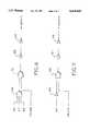
- FIG. 5provides a basic block diagram of the wordline driver.
- the wordline driverincludes a driver circuit which is implemented with inverter 300 having its output connected to wordline 301 and its input connected to node 302, which receives a wordline select signal from a decoder through an isolation circuit composed of transistor 303 formed in an isolated p-well.
- Transistor 303has its source connected to node 302 and its drain connected to the decode input 304.
- the gate of transistor 303is connected to a selector 305 which supplies either the signal PGMNVB on line 306 or the signal AVX on line 307.
- the driveralso includes circuitry for holding the value of the wordline select signal at node 302 when the isolation transistor 303 is non-conducting.
- This circuitconsists of inverter 308 which has its input connected to the wordline 301, and its output connected to node 302.
- the combination of inverters 300 and 308form a storage element.
- the power supply voltages AVX and PGMNVBare supplied through power supply selector circuitry 309 and 310, respectively. Although not shown, the selectors 309 and 310 are shared by a plurality of wordline drivers.
- the selector 309supplies a signal AVX on line 307 from among positive supply voltage V DD on line 325, a high positive voltage V POS on line 311, one or more intermediate positive voltages V INT+ on line 312, and ground on line 313, which provides a reference potential.
- the selector 310selects from among a negative potential V NEG on line 314, one or more intermediate negative voltages V INT- on line 315, and ground on line 316.
- the inverter 300operates to select either the value AVX for connection to the wordline 301, or the value PGMNVB for connection to the wordline 301 depending on the value of the wordline select signal from the decoder on line 304.
- the selectors 309, 310, and 305are operated to establish a program mode, a read mode, and an erase mode under control of a mode control state machine on the chip.
- the selector 309is operated to supply the high positive potential V POS to line 307 as the signal AVX.
- the selector 310is operated to supply ground to line 306 as the signal PGMNVB.
- the selected wordlinei.e. wordlines in a sector to be erased during the erase mode
- V POS+12 volts
- selector 309is operated to supply the value V DD as the signal AVX, and the selector 310 is operated to supply ground.
- the selector 309is operated to supply ground as the signal AVX, and the selector 310 is operated to supply the signal V NEG as the signal PGMNVB on line 306.
- the selectors 309 and 310are operated to select the signals V INT+ and V INT- during a transition from a read mode to a program mode, as explained in more detail below.
- the selector 305is operated to supply the signal AVX to a gate of transistor 303 during the read and erase modes, to leave transistor 303 in a conducting state.
- the signal PGMNVB on line 306is applied to the gate. This is guaranteed to be as low as or lower than the value on node 302, turning off transistor 303, and isolating node 302 from the decoder.
- the inverters 300 and 308are composed of a p-channel transistor in series with an n-channel transistor.
- the n-channel transistors for both invertersare implemented in isolated p-wells, like transistor 303.
- the p-channel transistors for both invertershave channels biased at voltage AVW (not shown), which is relevant to the operation described below.
- the wordline driver 600operates in three modes:
- the decoderapplies a positive voltage, setting a selected wordline to V DD . Only one wordline is selected to AVX which is set at V DD . The other wordlines are set at PGMNVB which is set at ground.
- the decoderapplies a positive voltage to selected wordlines at the high erase voltage level.
- Multiple wordline driverswhere each wordline driver may drive eight or more wordlines, are connected to the high erase voltage at the AVX terminal.
- a wordline set sequenceis used to latch the address decoder input data. The value of AVX is switched from the V DD level to the high erase voltage.
- the decoderapplies a negative voltage to a selected wordline, where the negative is the high negative voltage generated at PGMNVB.
- a selected wordlineis connected to PGMNVB, while all others are coupled to AVX.
- a wordline set mode WLSETall the wordlines are set to high read voltage V DD .
- the signal AVXis set at 5 V
- AVWn-well bias for p-channel devices in WL driver inverters 300 and 308
- PGMNVBis set at 0 V
- a state machinecontrols the decoders to sequentially flip the wordlines in the array to the positive value.
- a wordline select stepoccurs, in which one wordline driver is connected to the PGMNVB voltage.
- a supply shift stepis executed, which shifts the supply voltage AVX from +5 V to 0 V, and the supply voltage PGMNVB from 0, to -8 V. This shift is executed in a number of steps.
- a program sequenceis executed, in which the voltage AVX is 0 V, the voltage AVW is 3 V, and the PGMNVB voltage is -8 V on a selected wordline.
- a program reset sequenceis executed to move out of the program mode back to the read mode by changing the values PGMNVB to ground and AVX to +5 volts.
- the value PGMNVBis switched directly to 0 volts, and AVX is moved up to 3 volts.
- AVWis moved up to 5 volts.
- AVXis moved up to 5 volts, leaving the voltages set up for the normal read mode.
- each of the wordlinesmust be accessible during the wordline set step outlined above so that it can be set to a positive value prior to the supply shift step. If the wordlines were simply disconnected, as done in the prior art, then this process could not be carried out, and when the supply shift was executed, the supply voltage on the wordline driver for the disabled sector would be driven to the negative value.
- control logic associated with the sector decodermust be coupled with the mode control logic for the read/program and erase cycles on the device according to this aspect of the present invention.
- FIGS. 6 through 11illustrate the sector decoding logic for used according to a preferred embodiment of the present invention.
- FIG. 6a pre-decoding logic for address bits A16 through A18 is illustrated.
- FIG. 7shows the pre-decoding for A19.
- one of eight decodersis shown, in which three inputs to NAND gate 400 correspond to high or low states of address bits A16 through A18. It will be appreciated that eight different configurations of the input signals can be generated to the eight different pre-decoder stages.
- the output of the NAND gate 400is supplied to a two input NAND gate 401.
- the second input into the NAND gate 401is a control signal XBL3HB, which enables or disables sector decoding.
- the output of the NAND gate 401is supplied through inverters 402 and 403 to supply a pre-decode output signal XQ1 (0-7).
- Address bit A19is pre-decoded using the logic shown in FIG. 7. Thus, address bit A19 is supplied through inverter 405 to a first input of NAND gate 406. The second input of the NAND gate 406 is the control signal XBL3HB. The output of the NAND gate 406 is supplied through inverter 407 and inverter 408 to generate the decode signal XQ2 (0-1).
- the ten pre-decode signals XQ1 (0-7) and XQ2 (0-1)are supplied to a sector decoder which includes the logic shown in FIG. 8 for the upper half of the array, and the logic shown in FIG. 9 for the lower half of the array.
- a sector decoderwhich includes the logic shown in FIG. 8 for the upper half of the array, and the logic shown in FIG. 9 for the lower half of the array.
- XQ1(i)supplies a first input to NAND gate 450.
- the second input to NAND gate 450is the output of OR gate 440.
- a first input to OR gate 440is pre-decode signal XQ2(0).
- the second input to OR gate 440is the output of NOR gate 439, which has the inverse of the SCFGDIS signal (sector flag disable) from inverter 438 as one input, and the PGWLSR signal (indicating a page programming sequence) as a second input.
- the output of the NAND gate 450is supplied as a first input to NOR gate 451.
- the second input to NOR gate 451is the output of NOR gate 452.
- Inputs to NOR gate 452include the signal PGWLSR, and the output of NAND gate 453.
- NAND gate 453receives the configuration data, including a sector flag disable signal SCFGDIS, and a sector flag SCFG(i) signal for the corresponding sector. Also, when SCFGDIS is high and PGWLSR is low, NOR gate 439 generates a high output, overriding XQ2(0) during the page programming sequence when the array is segmented.
- NOR gate 451drives the string of inverters 454, 455, 456, 457 to generate the output signal XBL3U.
- the output of inverter 454is supplied as an input to NAND gate 458.
- the output of NAND gate 458is supplied through inverters 459, 460, and 461 to generate the output signal XBL3UB.
- the second input to NAND gate 458is the control signal XBDISB used during the program set up sequence.
- the sector flag disable signal SCFGDISwill be high, and the sector flag SCFG(i) will also be high for the bad sector. This will cause the output of the NAND gate 453 to be low, and the output of the NOR gate 452 to be high. This will disable NOR gate 451 from changing in response to the pre-decode signals XQ1(i) and XQ20 and isolate the bad sector. Also, when SCFGDIS is high and PGWLSR is low, NOR gate 439 generates a high output, overriding XQ2(0) during the page programming sequence when the array is segmented.
- the lower segment of the arrayis decoded using the logic of FIG. 9.
- the pre-decode signals XQ1(i) and XQ2(1)are supplied as inputs to NAND gate 475.
- the output of NAND gate 475is supplied as a first input to NOR gate 476.
- the second input of NOR gate 476is the output of AND gate 469.
- Inputs to AND gate 469include SCFGDIS and the inverse of PGWLSR through inverter 468.
- the output of NOR gate 476is a first input to NOR gate 477.
- the second input to NOR gate 477is the output of NOR gate 478.
- the inputs to NOR gate 478include the control signal PGWLSR, and the output of the NAND gate 479.
- NAND gate 479receives as inputs the pre-decode signal XQ1(i), the sector flag disable signal SCFGDIS, and the sector flag SCFG(i).
- the output of the NOR gate 477supplies the series including inverter 480, inverter 481, and inverter 482 which supplies the output signal XBL3D. Also the output of NOR gate 477 supplies a first input to NAND gate 483.
- the NAND gate 483drives a sequence of inverters 484, 485, and 486 which supplies the output signal XBL3DB.
- a control signal XBDISBis supplied as a second input to the NAND gate 483.
- the lower sectoris disabled in response to the sector flag disable signal SCFGDIS.
- SCFGDISis high, and PGWLSR is low
- the output of AND gate 469is high which causes the output of NOR gate 476 to be low overriding the address signals reflected in XQ1(i) and XQ2(1).
- the output of NOR gate 477is controlled by NAND gate 479 which changes if the corresponding sector is selected as indicated by SCFG(i) when SCFGDIS is high.
- the output of NOR gate 477changes with the control signal XQ1(i) while the corresponding sector in the top half is disabled (NAND gate 453 of FIG. 8). Else, the sector is disabled by NAND gate 479.
- the control signal PGWLSRis asserted in the program wordline set and reset sequence described above. Thus, the disabling of the sector decoder which occurs due to the configuration store is overridden during this sequence in response to this signal.
- the PGWLSR signalis generated using logic such as illustrated in FIG. 10, where control signals corresponding to the wordline set and wordline reset sequences are supplied as inputs to NOR gate 500.
- the output of the NOR gate 500is supplied as an input to NOR gate 501.
- the second input to NOR gate 501is supplied at the output of inverter 502 which receives as inputs the page program mode control signal.
- the output of the NOR gate 501is supplied through inverters 503 and 504 to generate the PGWLSR signal used in the logic of FIGS. 8 and 9.
- FIG. 11functionally illustrates the configuration store for the basic embodiment of FIGS. 2 and 7-10. As can be seen, it comprises a 9 bit non-volatile register, implemented using floating gate memory cells, fuses, on antifuses, laser cut nodes, or the like for the purposes of generating the sector flag signals SCFG(0) through SCFG(7), and the sector flag disable signal SCFGDIS.
- a segmentable high density memory devicesuch as a 16 megabit or higher flash EEPROM array
- a configuration storewhich is capable of configuring the sector level decoding of the device
- Die which would normally be discardedcan be reconfigured as a smaller device while preserving sequential addressing. With the sequential addressing, the die can be packaged as if it were a smaller device, and sold.
- the sector level decodingallows for sophisticated reconfiguration of the array without the necessity of complex wiring steps in the manufacture to make sure that a particular address buffer is coupled to a particular address pin as would be required using the prior art approach.
- the present inventionis particularly significant because of the small amount of logic required to implement it, requiring very little real estate on the integrated circuit.
- high density memory devicesin which chip area is at a premium, can be effectively and inexpensively provided with tools needed for reconfiguring bad high density devices as a good lower density devices, thereby improving manufacturing yield and reducing waste.
Landscapes
- Engineering & Computer Science (AREA)
- Microelectronics & Electronic Packaging (AREA)
- For Increasing The Reliability Of Semiconductor Memories (AREA)
Abstract
Description
Claims (25)
Priority Applications (1)
| Application Number | Priority Date | Filing Date | Title |
|---|---|---|---|
| US08/605,100US5691945A (en) | 1995-05-31 | 1995-05-31 | Technique for reconfiguring a high density memory |
Applications Claiming Priority (2)
| Application Number | Priority Date | Filing Date | Title |
|---|---|---|---|
| PCT/US1995/006990WO1996038845A1 (en) | 1995-05-31 | 1995-05-31 | Technique for reconfiguring a high density memory |
| US08/605,100US5691945A (en) | 1995-05-31 | 1995-05-31 | Technique for reconfiguring a high density memory |
Publications (1)
| Publication Number | Publication Date |
|---|---|
| US5691945Atrue US5691945A (en) | 1997-11-25 |
Family
ID=24422267
Family Applications (1)
| Application Number | Title | Priority Date | Filing Date |
|---|---|---|---|
| US08/605,100Expired - LifetimeUS5691945A (en) | 1995-05-31 | 1995-05-31 | Technique for reconfiguring a high density memory |
Country Status (1)
| Country | Link |
|---|---|
| US (1) | US5691945A (en) |
Cited By (42)
| Publication number | Priority date | Publication date | Assignee | Title |
|---|---|---|---|---|
| US5831914A (en)* | 1997-03-31 | 1998-11-03 | International Business Machines Corporation | Variable size redundancy replacement architecture to make a memory fault-tolerant |
| US5831913A (en)* | 1997-03-31 | 1998-11-03 | International Business Machines Corporation | Method of making a memory fault-tolerant using a variable size redundancy replacement configuration |
| US5862088A (en)* | 1997-04-14 | 1999-01-19 | Advantest Corporation | Apparatus and method for testing a memory |
| US5883842A (en)* | 1996-04-11 | 1999-03-16 | Mitsubishi Denki Kabushiki Kaisha | Memory card having block erasure type memory units which are used even when partially defective |
| US5903488A (en)* | 1995-07-03 | 1999-05-11 | Oki Electric Industry Co.,Ltd. | Semiconductor memory with improved word line structure |
| EP0926601A1 (en)* | 1997-12-24 | 1999-06-30 | STMicroelectronics S.r.l. | Data protection method for a semiconductor memory and corresponding protected memory device |
| US5978931A (en)* | 1997-07-16 | 1999-11-02 | International Business Machines Corporation | Variable domain redundancy replacement configuration for a memory device |
| US5978298A (en)* | 1996-08-01 | 1999-11-02 | Micron Technology, Inc. | Shared pull-up and selection circuitry for programmable cells such as antifuse cells |
| US6006313A (en)* | 1995-06-19 | 1999-12-21 | Sharp Kabushiki Kaisha | Semiconductor memory device that allows for reconfiguration around defective zones in a memory array |
| US6018811A (en)* | 1996-04-25 | 2000-01-25 | Micron Technology, Inc. | Layout for semiconductor memory device wherein intercoupling lines are shared by two sets of fuse banks and two sets of redundant elements not simultaneously active |
| WO2000017886A1 (en)* | 1998-09-23 | 2000-03-30 | Advanced Micro Devices, Inc. | Bank selector circuit for a simultaneous operation flash memory device with a flexible bank partition architecture |
| US6097661A (en)* | 1997-09-26 | 2000-08-01 | Siemens Aktiengesellschaft | Pointer circuit with low surface requirement high speed and low power loss |
| US6118711A (en)* | 1996-04-16 | 2000-09-12 | Micron Technology, Inc. | Apparatus for testing redundant elements in a packaged semiconductor memory device |
| US6122194A (en)* | 1997-12-29 | 2000-09-19 | Samsung Electronics, Co., Ltd. | Semiconductor memory device with a column redundancy occupying a less chip area |
| US6154862A (en)* | 1996-11-01 | 2000-11-28 | Advantest Corporation | Defect analysis memory for memory tester |
| US6188619B1 (en)* | 1998-10-09 | 2001-02-13 | Samsung Electronics Co., Ltd. | Memory device with address translation for skipping failed memory blocks |
| US6212482B1 (en) | 1998-03-06 | 2001-04-03 | Micron Technology, Inc. | Circuit and method for specifying performance parameters in integrated circuits |
| US6223301B1 (en)* | 1997-09-30 | 2001-04-24 | Compaq Computer Corporation | Fault tolerant memory |
| US6256234B1 (en) | 1997-02-11 | 2001-07-03 | Micron Technology, Inc. | Low skew differential receiver with disable feature |
| US6330688B1 (en)* | 1995-10-31 | 2001-12-11 | Intel Corporation | On chip error correction for devices in a solid state drive |
| US6349237B1 (en) | 1997-12-23 | 2002-02-19 | The Regents Of The University Of Michigan | Reconfigurable manufacturing system having a production capacity method for designing same and method for changing its production capacity |
| US6381192B1 (en)* | 1999-12-28 | 2002-04-30 | Hyundai Electronics Industries Co., Ltd. | Address buffer in a flash memory |
| US6452845B1 (en) | 1999-01-07 | 2002-09-17 | Micron Technology, Inc. | Apparatus for testing redundant elements in a packaged semiconductor memory device |
| US20030026147A1 (en)* | 2001-08-02 | 2003-02-06 | Samsung Electronics Co., Ltd. | Fuse box including make-link and redundant address decoder having the same, and method for repairing defective memory cell |
| US6591327B1 (en)* | 1999-06-22 | 2003-07-08 | Silicon Storage Technology, Inc. | Flash memory with alterable erase sector size |
| US20030136976A1 (en)* | 2001-09-05 | 2003-07-24 | Toru Tanzawa | Nonvolatile semiconductor memory with a page mode |
| US6643196B2 (en)* | 2001-03-09 | 2003-11-04 | Oki Electric Industry Co., Ltd. | Redundant memory circuit for analog semiconductor memory |
| US6693831B2 (en) | 2000-08-03 | 2004-02-17 | Samsung Electronics Co., Ltd. | Apparatus of repairing memory cell and method therefor |
| US6889307B1 (en) | 2001-11-16 | 2005-05-03 | Matrix Semiconductor, Inc. | Integrated circuit incorporating dual organization memory array |
| US20050270841A1 (en)* | 2004-06-07 | 2005-12-08 | Merritt Todd A | Method and apparatus for semiconductor device repair with reduced number of programmable elements |
| US7006394B2 (en)* | 2004-06-07 | 2006-02-28 | Micron Technology, Inc. | Apparatus and method for semiconductor device repair with reduced number of programmable elements |
| US20060083087A1 (en)* | 2004-06-07 | 2006-04-20 | Cowles Timothy B | Apparatus and method for semiconductor device repair with reduced number of programmable elements |
| US20070147161A1 (en)* | 2005-12-27 | 2007-06-28 | Samsung Electronics Co., Ltd. | Semiconductor memory device having layout for minimizing area of sense amplifier region and word line driver region |
| US20070165461A1 (en)* | 2006-01-18 | 2007-07-19 | Cornwell Michael J | Disabling faulty flash memory dies |
| US7260019B1 (en)* | 2005-10-31 | 2007-08-21 | Spansion Llc | Memory array |
| US7277337B1 (en)* | 2006-09-25 | 2007-10-02 | Kingston Technology Corp. | Memory module with a defective memory chip having defective blocks disabled by non-multiplexed address lines to the defective chip |
| US20090003098A1 (en)* | 2007-06-26 | 2009-01-01 | Benedikt Hoess | Method for Hiding Defective Memory Cells and Semiconductor Memories |
| US20090147579A1 (en)* | 1999-01-14 | 2009-06-11 | Silicon Storage Technology, Inc. | Non-volatile memory systems and methods including page read and/or configuration features |
| US20100232223A1 (en)* | 2008-11-12 | 2010-09-16 | Yu-Mao Kao | Defective block handling method for a multiple data channel flash memory storege device |
| US8288206B2 (en) | 1997-04-04 | 2012-10-16 | Elm Technology Corp | Three dimensional structure memory |
| US20160077906A1 (en)* | 2014-09-12 | 2016-03-17 | Ross S. Scouller | High voltage failure recovery for emulated electrically erasable (eee) memory system |
| US10109344B2 (en) | 2015-12-30 | 2018-10-23 | Samsung Electronics Co., Ltd. | Semiconductor memory devices with banks with different numbers of memory cells coupled to their bit-lines and memory systems including the same |
Citations (5)
| Publication number | Priority date | Publication date | Assignee | Title |
|---|---|---|---|---|
| US5126973A (en)* | 1990-02-14 | 1992-06-30 | Texas Instruments Incorporated | Redundancy scheme for eliminating defects in a memory device |
| US5392247A (en)* | 1991-09-19 | 1995-02-21 | Mitsubishi Denki Kabushiki Kaisha | Semiconductor memory device including redundancy circuit |
| US5394368A (en)* | 1991-08-28 | 1995-02-28 | Oki Electric Industry Co., Ltd. | Semiconductor memory device |
| US5481498A (en)* | 1991-07-11 | 1996-01-02 | Goldstar Electron Co., Ltd. | Redundancy circuit for semiconductor memory device |
| US5544113A (en)* | 1994-11-30 | 1996-08-06 | International Business Machines Corporation | Random access memory having a flexible array redundancy scheme |
- 1995
- 1995-05-31USUS08/605,100patent/US5691945A/ennot_activeExpired - Lifetime
Patent Citations (5)
| Publication number | Priority date | Publication date | Assignee | Title |
|---|---|---|---|---|
| US5126973A (en)* | 1990-02-14 | 1992-06-30 | Texas Instruments Incorporated | Redundancy scheme for eliminating defects in a memory device |
| US5481498A (en)* | 1991-07-11 | 1996-01-02 | Goldstar Electron Co., Ltd. | Redundancy circuit for semiconductor memory device |
| US5394368A (en)* | 1991-08-28 | 1995-02-28 | Oki Electric Industry Co., Ltd. | Semiconductor memory device |
| US5392247A (en)* | 1991-09-19 | 1995-02-21 | Mitsubishi Denki Kabushiki Kaisha | Semiconductor memory device including redundancy circuit |
| US5544113A (en)* | 1994-11-30 | 1996-08-06 | International Business Machines Corporation | Random access memory having a flexible array redundancy scheme |
Cited By (86)
| Publication number | Priority date | Publication date | Assignee | Title |
|---|---|---|---|---|
| US6006313A (en)* | 1995-06-19 | 1999-12-21 | Sharp Kabushiki Kaisha | Semiconductor memory device that allows for reconfiguration around defective zones in a memory array |
| US5903488A (en)* | 1995-07-03 | 1999-05-11 | Oki Electric Industry Co.,Ltd. | Semiconductor memory with improved word line structure |
| US6438706B1 (en)* | 1995-10-31 | 2002-08-20 | Intel Corporation | On chip error correction for devices in a solid state drive |
| US6330688B1 (en)* | 1995-10-31 | 2001-12-11 | Intel Corporation | On chip error correction for devices in a solid state drive |
| US5883842A (en)* | 1996-04-11 | 1999-03-16 | Mitsubishi Denki Kabushiki Kaisha | Memory card having block erasure type memory units which are used even when partially defective |
| US6118711A (en)* | 1996-04-16 | 2000-09-12 | Micron Technology, Inc. | Apparatus for testing redundant elements in a packaged semiconductor memory device |
| US6560728B2 (en) | 1996-04-25 | 2003-05-06 | Micron Technology, Inc. | Layout for semiconductor memory device having a plurality of rows and columns of circuit cells divided into first and second planes that are not simultaneously active |
| US7043672B2 (en) | 1996-04-25 | 2006-05-09 | Micron Technology, Inc. | Layout for a semiconductor memory device having redundant elements |
| US6018811A (en)* | 1996-04-25 | 2000-01-25 | Micron Technology, Inc. | Layout for semiconductor memory device wherein intercoupling lines are shared by two sets of fuse banks and two sets of redundant elements not simultaneously active |
| US5978298A (en)* | 1996-08-01 | 1999-11-02 | Micron Technology, Inc. | Shared pull-up and selection circuitry for programmable cells such as antifuse cells |
| US6011742A (en)* | 1996-08-01 | 2000-01-04 | Micron Technology, Inc. | Shared pull-up and selection circuitry for programmable cells such as antifuse cells |
| US6154862A (en)* | 1996-11-01 | 2000-11-28 | Advantest Corporation | Defect analysis memory for memory tester |
| US6256234B1 (en) | 1997-02-11 | 2001-07-03 | Micron Technology, Inc. | Low skew differential receiver with disable feature |
| US5940335A (en)* | 1997-03-31 | 1999-08-17 | International Business Machines Corporation | Prioritizing the repair of faults in a semiconductor memory device |
| US5831913A (en)* | 1997-03-31 | 1998-11-03 | International Business Machines Corporation | Method of making a memory fault-tolerant using a variable size redundancy replacement configuration |
| US5831914A (en)* | 1997-03-31 | 1998-11-03 | International Business Machines Corporation | Variable size redundancy replacement architecture to make a memory fault-tolerant |
| US8318538B2 (en) | 1997-04-04 | 2012-11-27 | Elm Technology Corp. | Three dimensional structure memory |
| US8791581B2 (en) | 1997-04-04 | 2014-07-29 | Glenn J Leedy | Three dimensional structure memory |
| US8796862B2 (en) | 1997-04-04 | 2014-08-05 | Glenn J Leedy | Three dimensional memory structure |
| US8841778B2 (en) | 1997-04-04 | 2014-09-23 | Glenn J Leedy | Three dimensional memory structure |
| US8410617B2 (en) | 1997-04-04 | 2013-04-02 | Elm Technology | Three dimensional structure memory |
| US8907499B2 (en) | 1997-04-04 | 2014-12-09 | Glenn J Leedy | Three dimensional structure memory |
| US9087556B2 (en) | 1997-04-04 | 2015-07-21 | Glenn J Leedy | Three dimension structure memory |
| US8288206B2 (en) | 1997-04-04 | 2012-10-16 | Elm Technology Corp | Three dimensional structure memory |
| US5862088A (en)* | 1997-04-14 | 1999-01-19 | Advantest Corporation | Apparatus and method for testing a memory |
| SG79234A1 (en)* | 1997-07-16 | 2001-03-20 | Ibm | Variable domain redundancy replacement configuration for a memory device |
| US5978931A (en)* | 1997-07-16 | 1999-11-02 | International Business Machines Corporation | Variable domain redundancy replacement configuration for a memory device |
| US6097661A (en)* | 1997-09-26 | 2000-08-01 | Siemens Aktiengesellschaft | Pointer circuit with low surface requirement high speed and low power loss |
| US7409581B2 (en) | 1997-09-30 | 2008-08-05 | Hewlett-Packard Development Company, L.P. | Main memory controller adapted to correct corrupted data by xoring corrupted data to directly generate correct data |
| US6223301B1 (en)* | 1997-09-30 | 2001-04-24 | Compaq Computer Corporation | Fault tolerant memory |
| US20020194530A1 (en)* | 1997-09-30 | 2002-12-19 | Santeler Paul A. | Fault tolerant memory |
| US6430702B1 (en) | 1997-09-30 | 2002-08-06 | Compaq Computer Corporation | Fault tolerant memory |
| US6349237B1 (en) | 1997-12-23 | 2002-02-19 | The Regents Of The University Of Michigan | Reconfigurable manufacturing system having a production capacity method for designing same and method for changing its production capacity |
| US6286086B1 (en) | 1997-12-24 | 2001-09-04 | Stmicroelectronics S.R.L. | Data protection method for a semiconductor memory and corresponding protected memory device |
| EP0926601A1 (en)* | 1997-12-24 | 1999-06-30 | STMicroelectronics S.r.l. | Data protection method for a semiconductor memory and corresponding protected memory device |
| US6122194A (en)* | 1997-12-29 | 2000-09-19 | Samsung Electronics, Co., Ltd. | Semiconductor memory device with a column redundancy occupying a less chip area |
| US6212482B1 (en) | 1998-03-06 | 2001-04-03 | Micron Technology, Inc. | Circuit and method for specifying performance parameters in integrated circuits |
| US6393378B2 (en) | 1998-03-06 | 2002-05-21 | Micron Technology, Inc. | Circuit and method for specifying performance parameters in integrated circuits |
| US6275894B1 (en) | 1998-09-23 | 2001-08-14 | Advanced Micro Devices, Inc. | Bank selector circuit for a simultaneous operation flash memory device with a flexible bank partition architecture |
| US6633949B2 (en) | 1998-09-23 | 2003-10-14 | Advanced Micro Devices, Inc. | Bank selector circuit for a simultaneous operation flash memory device with a flexible bank partition architecture |
| WO2000017886A1 (en)* | 1998-09-23 | 2000-03-30 | Advanced Micro Devices, Inc. | Bank selector circuit for a simultaneous operation flash memory device with a flexible bank partition architecture |
| US6470414B2 (en) | 1998-09-23 | 2002-10-22 | Advanced Micro Devices, Inc. | Bank selector circuit for a simultaneous operation flash memory device with a flexible bank partition architecture |
| US6188619B1 (en)* | 1998-10-09 | 2001-02-13 | Samsung Electronics Co., Ltd. | Memory device with address translation for skipping failed memory blocks |
| US6452845B1 (en) | 1999-01-07 | 2002-09-17 | Micron Technology, Inc. | Apparatus for testing redundant elements in a packaged semiconductor memory device |
| US8614924B2 (en) | 1999-01-14 | 2013-12-24 | Silicon Storage Technology, Inc. | Non-volatile memory systems and methods |
| US9640263B2 (en) | 1999-01-14 | 2017-05-02 | Silicon Storage Technology, Inc. | Non-volatile memory systems and methods |
| US8432750B2 (en) | 1999-01-14 | 2013-04-30 | Silicon Storage Technology, Inc. | Non-volatile memory systems and methods including page read and/or configuration features |
| US7848159B2 (en)* | 1999-01-14 | 2010-12-07 | Silicon Storage Technology, Inc. | Non-volatile memory systems and methods including page read and/or configuration features |
| US20090147579A1 (en)* | 1999-01-14 | 2009-06-11 | Silicon Storage Technology, Inc. | Non-volatile memory systems and methods including page read and/or configuration features |
| US6591327B1 (en)* | 1999-06-22 | 2003-07-08 | Silicon Storage Technology, Inc. | Flash memory with alterable erase sector size |
| US6381192B1 (en)* | 1999-12-28 | 2002-04-30 | Hyundai Electronics Industries Co., Ltd. | Address buffer in a flash memory |
| US6836441B2 (en) | 2000-08-03 | 2004-12-28 | Samsung Electronics Co., Ltd. | Apparatus of repairing memory cell and method therefor |
| US20040081007A1 (en)* | 2000-08-03 | 2004-04-29 | Samsung Electronics Co., Ltd. | Apparatus of repairing memory cell and method therefor |
| US6693831B2 (en) | 2000-08-03 | 2004-02-17 | Samsung Electronics Co., Ltd. | Apparatus of repairing memory cell and method therefor |
| US6643196B2 (en)* | 2001-03-09 | 2003-11-04 | Oki Electric Industry Co., Ltd. | Redundant memory circuit for analog semiconductor memory |
| US6850450B2 (en)* | 2001-08-02 | 2005-02-01 | Samsung Electronics Co., Ltd. | Fuse box including make-link and redundant address decoder having the same, and method for repairing defective memory cell |
| US20030026147A1 (en)* | 2001-08-02 | 2003-02-06 | Samsung Electronics Co., Ltd. | Fuse box including make-link and redundant address decoder having the same, and method for repairing defective memory cell |
| US6781879B2 (en)* | 2001-09-05 | 2004-08-24 | Kabushiki Kaisha Toshiba | Nonvolatile semiconductor memory with a page mode |
| US20030136976A1 (en)* | 2001-09-05 | 2003-07-24 | Toru Tanzawa | Nonvolatile semiconductor memory with a page mode |
| US20040252552A1 (en)* | 2001-09-05 | 2004-12-16 | Kabushiki Kaisha Toshiba | Nonvolatile semiconductor memory with a page mode |
| US6889307B1 (en) | 2001-11-16 | 2005-05-03 | Matrix Semiconductor, Inc. | Integrated circuit incorporating dual organization memory array |
| US7218561B2 (en) | 2004-06-07 | 2007-05-15 | Micron Technology, Inc. | Apparatus and method for semiconductor device repair with reduced number of programmable elements |
| US20050270841A1 (en)* | 2004-06-07 | 2005-12-08 | Merritt Todd A | Method and apparatus for semiconductor device repair with reduced number of programmable elements |
| US7006393B2 (en)* | 2004-06-07 | 2006-02-28 | Micron Technology, Inc. | Method and apparatus for semiconductor device repair with reduced number of programmable elements |
| US7006394B2 (en)* | 2004-06-07 | 2006-02-28 | Micron Technology, Inc. | Apparatus and method for semiconductor device repair with reduced number of programmable elements |
| US7376025B2 (en) | 2004-06-07 | 2008-05-20 | Micron Technology, Inc. | Method and apparatus for semiconductor device repair with reduced number of programmable elements |
| US20060083087A1 (en)* | 2004-06-07 | 2006-04-20 | Cowles Timothy B | Apparatus and method for semiconductor device repair with reduced number of programmable elements |
| US20060120187A1 (en)* | 2004-06-07 | 2006-06-08 | Merritt Todd A | Method and apparatus for semiconductor device repair with reduced number of programmable elements |
| KR100964352B1 (en) | 2005-10-31 | 2010-06-17 | 스펜션 엘엘씨 | Memory arrays and associated decoders arranged in banks and sectors |
| US7260019B1 (en)* | 2005-10-31 | 2007-08-21 | Spansion Llc | Memory array |
| CN104299638B (en)* | 2005-10-31 | 2018-02-09 | 赛普拉斯半导体公司 | Configuration is in thesaurus and sector and the memory array associated with decoder |
| US7359273B2 (en)* | 2005-12-27 | 2008-04-15 | Samsung Electronics Co., Ltd. | Semiconductor memory device having layout for minimizing area of sense amplifier region and word line driver region |
| US20070147161A1 (en)* | 2005-12-27 | 2007-06-28 | Samsung Electronics Co., Ltd. | Semiconductor memory device having layout for minimizing area of sense amplifier region and word line driver region |
| US7609561B2 (en)* | 2006-01-18 | 2009-10-27 | Apple Inc. | Disabling faulty flash memory dies |
| US20100002512A1 (en)* | 2006-01-18 | 2010-01-07 | Cornwell Michael J | Disabling faulty flash memory dies |
| JP2011108267A (en)* | 2006-01-18 | 2011-06-02 | Apple Inc | Disabling faulty flash memory die |
| US20070165461A1 (en)* | 2006-01-18 | 2007-07-19 | Cornwell Michael J | Disabling faulty flash memory dies |
| US8055959B2 (en)* | 2006-01-18 | 2011-11-08 | Apple Inc. | Disabling faulty flash memory dies |
| US7277337B1 (en)* | 2006-09-25 | 2007-10-02 | Kingston Technology Corp. | Memory module with a defective memory chip having defective blocks disabled by non-multiplexed address lines to the defective chip |
| DE102007029371A1 (en)* | 2007-06-26 | 2009-01-02 | Qimonda Ag | Method for concealing defective memory cells and semiconductor memory |
| US20090003098A1 (en)* | 2007-06-26 | 2009-01-01 | Benedikt Hoess | Method for Hiding Defective Memory Cells and Semiconductor Memories |
| US7839684B2 (en)* | 2008-11-12 | 2010-11-23 | Skymedi Corporation | Defective block handling method for a multiple data channel flash memory storage device |
| US20100232223A1 (en)* | 2008-11-12 | 2010-09-16 | Yu-Mao Kao | Defective block handling method for a multiple data channel flash memory storege device |
| US20160077906A1 (en)* | 2014-09-12 | 2016-03-17 | Ross S. Scouller | High voltage failure recovery for emulated electrically erasable (eee) memory system |
| US9563491B2 (en)* | 2014-09-12 | 2017-02-07 | Nxp Usa, Inc. | High voltage failure recovery for emulated electrically erasable (EEE) memory system |
| US10109344B2 (en) | 2015-12-30 | 2018-10-23 | Samsung Electronics Co., Ltd. | Semiconductor memory devices with banks with different numbers of memory cells coupled to their bit-lines and memory systems including the same |
Similar Documents
| Publication | Publication Date | Title |
|---|---|---|
| US5691945A (en) | Technique for reconfiguring a high density memory | |
| KR100200985B1 (en) | Redundant circuit device | |
| EP0422347B1 (en) | Bitline segmentation in logic memory arrays | |
| US6532181B2 (en) | Semiconductor memory device having redundant circuitry for replacing defective memory cell | |
| US5548225A (en) | Block specific spare circuit | |
| US5920503A (en) | Flash memory with novel bitline decoder and sourceline latch | |
| JP3351595B2 (en) | Semiconductor memory device | |
| US5287310A (en) | Memory with I/O mappable redundant columns | |
| US5485424A (en) | Semiconductor memory and redundant-address writing method | |
| JP2791288B2 (en) | Method of programming a redundant register in a row redundant integrated circuit for a semiconductor memory device and a row redundant integrated circuit | |
| US20080279020A1 (en) | Semiconductor memory device | |
| US5602786A (en) | Method for programming redundancy registers in a column redundancy integrated circuitry for a semiconductor memory device, and column redundancy integrated circuitry | |
| EP0940753B1 (en) | Semiconductor memory device with redundancy | |
| US5847999A (en) | Integrated circuit memory devices having variable block size erase capability | |
| US5272672A (en) | Semiconductor memory device having redundant circuit | |
| US6498756B2 (en) | Semiconductor memory device having row repair circuitry | |
| EP0661636B1 (en) | Integrated programming circuitry for an electrically programmable semiconductor memory device with redundancy | |
| EP0905704A1 (en) | Sectored semiconductor memory device with configurable memory sector addresses | |
| US6122200A (en) | Row decoder for a flash-EEPROM memory device with the possibility of selective erasing of a sub-group of rows of a sector | |
| US5787043A (en) | Semiconductor memory device having a redundancy capability | |
| EP1717818B1 (en) | Semiconductor storage device and redundancy method for semiconductor storage device | |
| EP0675440B1 (en) | Redundancy circuitry for a semiconductor memory device | |
| EP0829086B1 (en) | Technique for reconfiguring a high density memory | |
| US6813198B2 (en) | Semiconductor memory device and method of repairing the same | |
| US7009910B2 (en) | Semiconductor memory having a flexible dual-bank architecture with improved row decoding |
Legal Events
| Date | Code | Title | Description |
|---|---|---|---|
| AS | Assignment | Owner name:MACRONIX INTERNATIONAL CO., LTD., TAIWAN Free format text:ASSIGNMENT OF ASSIGNORS INTEREST;ASSIGNOR:LIN, TIEN-LER;REEL/FRAME:008130/0041 Effective date:19960112 Owner name:MACRONIX INTERNATIONAL CO. LTD, TAIWAN Free format text:ASSIGNMENT OF ASSIGNORS INTEREST;ASSIGNORS:LIOU, KONG-MOU;WAN, RAY-LIN;CHENG, YAO-WU;AND OTHERS;REEL/FRAME:008130/0014 Effective date:19960202 Owner name:MACRONIX INTERNATIONAL, CO., LTD., TAIWAN Free format text:ASSIGNMENT OF ASSIGNORS INTEREST;ASSIGNORS:YIU, TOM DANG-HSING;HUNG, CHUN-HSIUNG;REEL/FRAME:008129/0368 Effective date:19960122 | |
| STCF | Information on status: patent grant | Free format text:PATENTED CASE | |
| FEPP | Fee payment procedure | Free format text:PAYOR NUMBER ASSIGNED (ORIGINAL EVENT CODE: ASPN); ENTITY STATUS OF PATENT OWNER: LARGE ENTITY | |
| FPAY | Fee payment | Year of fee payment:4 | |
| FPAY | Fee payment | Year of fee payment:8 | |
| FPAY | Fee payment | Year of fee payment:12 |