US5691664A - Programmable analog array and method for establishing a feedback loop therein - Google Patents
Programmable analog array and method for establishing a feedback loop thereinDownload PDFInfo
- Publication number
- US5691664A US5691664AUS08/586,503US58650396AUS5691664AUS 5691664 AUS5691664 AUS 5691664AUS 58650396 AUS58650396 AUS 58650396AUS 5691664 AUS5691664 AUS 5691664A
- Authority
- US
- United States
- Prior art keywords
- cell
- circuitry
- analog
- output
- array
- Prior art date
- Legal status (The legal status is an assumption and is not a legal conclusion. Google has not performed a legal analysis and makes no representation as to the accuracy of the status listed.)
- Expired - Lifetime
Links
Images

Classifications
- H—ELECTRICITY
- H03—ELECTRONIC CIRCUITRY
- H03K—PULSE TECHNIQUE
- H03K19/00—Logic circuits, i.e. having at least two inputs acting on one output; Inverting circuits
- H03K19/02—Logic circuits, i.e. having at least two inputs acting on one output; Inverting circuits using specified components
- H03K19/173—Logic circuits, i.e. having at least two inputs acting on one output; Inverting circuits using specified components using elementary logic circuits as components
- H03K19/177—Logic circuits, i.e. having at least two inputs acting on one output; Inverting circuits using specified components using elementary logic circuits as components arranged in matrix form
- H03K19/17704—Logic circuits, i.e. having at least two inputs acting on one output; Inverting circuits using specified components using elementary logic circuits as components arranged in matrix form the logic functions being realised by the interconnection of rows and columns
Definitions
- the present inventionrelates, in general, to semiconductor integrated circuits and, more particularly, to semiconductor integrated circuits which are configurable for a wide range of functional applications.
- Integrated circuitsare popular in electronics applications because they are more compact and reliable than discrete components mounted on printed circuit boards. Many integrated circuits are designed and manufactured exclusively for a particular application. The process of designing a new integrated circuit and implementing a new design in wafer production is usually very costly.
- One approach for reducing costis to develop semiconductor integrated circuits which are configurable for a wide range of functional applications without the requirement for any major change in the manufacturing processes of the integrated circuits.
- One such integrated circuitcomprises an array of configurable analog cells. Each cell is capable of being internally configured in accordance with cell configuration data and being interconnected with other cells in the array through interconnection circuitry.
- the configuration of an analog cellcan be achieved using switched capacitor technology.
- the arraycan implement different analog functional applications such as amplifiers, filters, rectifiers, oscillators, etc. by using different internal configurations of the cells in the array and different interconnections among cells in the array. Achieving feedback for such functions as an automatic gain control loop in an amplifier requires the configuration information of the amplifier to be updated dynamically.
- an analog signalsuch as the signal at the output of an amplifier configured in the array
- the custom designed circuitconverts the analog signal into a digital configuration signal, which is transmitted back to the array by a global data bus.
- transmitting signals between the analog cells in the array and the circuit outside the arrayis slow and requires a large global data bus.
- establishing a feedback loop to control a switched capacitor circuit having eight bit programmable capacitorsrequires an eight bit parallel data bus.
- controlling a switched capacitor circuit in each cellrequires a parallel global data bus as large as 392 bits.
- the use of global busesreduces the bandwidth of signal transmission compared with local connections.
- each cell in the arrayincludes analog circuitry and digital circuitry so that a local feedback loop can be established within one cell or among neighboring cells in the array. It would be of further advantage for the feedback loop to be implemented within the programmable analog array and without using global data bus, thereby increasing the speed of signal transmission and reducing the size and manufacturing cost of the integrated circuit chip.
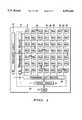
- FIG. 1is a block diagram of a programmable analog array in a representative arrangement in accordance with an embodiment of the present invention
- FIG. 2is a block diagram of a cell in the programmable analog array of FIG. 1;
- FIG. 3is a schematic diagram of an automatic gain control circuit implemented using two cells in the programmable analog array of FIG. 1;
- FIG. 4is a schematic diagram of a phase locked loop implemented using two cells in the programmable analog array of FIG. 1;
- FIG. 5is a flow chart of a method for establishing a feedback loop for use with the programable analog array of FIG. 1.
- FIG. 1is a block diagram of a programmable analog array 10 in a representative arrangement in accordance with an embodiment of the present invention.
- Programmable analog array 10comprises an array of cells 11 arranged in seven rows and seven columns.
- Each cell 11contains analog circuitry, digital circuitry, switch circuitry, and a memory unit, and will be further described with reference to FIG. 2.
- the switch circuitryconfigures the analog circuitry and digital circuitry in accordance with cell configuration data stored in the memory unit in each cell 11.
- the configuration of circuitryincludes coupling various components of the circuitry to each other and assigning component values to the various components. Examples of component values include the capacitance of a switched capacitor, the gain of an amplifier, the intrinsic frequency of an oscillator, or the like.
- Programmable analog array 10also includes a data storage element such as a random access memory (RAM) 22.
- RAM 22stores the cell configuration data for each cell 11 and the interconnection data for interconnecting different cells in programable analog array 10.
- the cell configuration data and the interconnection data stored in RAM 22can be reconfigured from an external source (not shown in FIG. 1) in order to implement new functional applications for programmable analog array 10.
- Programmable analog array 10further includes an accessing circuit 23 for selecting and accessing cells 11.
- Accessing circuit 23includes a control circuit 24 and programming shift registers 25 and 26.
- Programming shift registers 25 and 26are under the control of control circuit 24.
- Programming shift register 25provides a column coordinate reference signal
- programming shift register 26provides a row coordinate reference signal.
- the column and row coordinate reference signalsallow any cell 11 within programmable analog array 10 to be selected for access. After a cell 11 is selected, the cell configuration data stored in RAM 22 is transmitted to the memory unit in the selected cell 11 via accessing circuit 23.
- Interconnection circuitry 28establishes interconnection between different cells 11 in programmable analog array 10 in accordance with the interconnection data stored in RAM 22.
- interconnection circuitry 28may include a conducting metal network combined with switches. The interconnection data are continuously read by interconnection circuitry 28 to maintain the proper interconnection within programmable analog array 10.
- Programmable analog array 10further includes an input/output circuit 29.
- Input/output circuit 29transmits analog signals between programmable analog array 10 and external circuitry (not shown in FIG. 1) via an input/output port 27.
- programmable analog array 10is described in FIG. 1 as including seven rows and seven columns of cells 11, this is not intended as a limitation of the present invention.
- Programmable analog array 10may include any number of cells, e.g., eight rows and eight columns, four rows and five columns, etc., depending on its desired functional applications.
- the cells in the array of programmable analog array 10are not limited to being identical to each other in the present invention.
- the array in programable analog array 10may include cells which are structurally different from one another. For example, cells in the first, third, fifth, and seventh columns may be structurally identical to each other, whereas cells in the second, fourth, and sixth columns may be structurally identical to each other but structurally different from the cells in the first, third, fifth, and seventh columns.
- FIG. 2is a block diagram of a cell 11 in programmable analog array 10 of FIG. 1.
- Cell 11includes analog circuitry 12, digital circuitry 14, switch circuitry 15, and a memory unit 16.
- Analog circuitry 12may include an amplifier and an analog circuit element having internal components with variable connections such as a switched capacitor.
- Memory unit 16receives the cell configuration data from RAM 22 via programing shift registers 25 and 26.
- Switch circuitry 15maintains circuit configurations and component values in analog circuitry 12 and digital circuitry 14 to implement one of a plurality of circuit functions in accordance with the cell configuration data stored in memory unit 16. Nodes 18 and 19 are coupled to other cells in programable analog array 10 via interconnection circuitry 28.
- Digital circuitry 14converts an analog signal received from analog circuitry 12 into digital control information. The digital control information is transmitted to memory unit 16 to update the cell configuration data, thereby altering the configuration and/or adjusting the component values in analog circuitry 12. Therefore, digital circuitry 14 and analog circuitry 12 form a digital feedback loop.
- the analog circuitry in one cell of cells 11is not limited to forming a digital feedback loop with the digital circuitry in the same cell.
- a digital feedback loopmay be formed among two or more cells in the programable analog array 10.
- the analog circuitry and the digital circuitryare not limited to being included in the same cell in the array of programmable analog array 10.
- the cells in the first, third, fifth, and seventh cellsinclude the analog circuitry
- the cells in the second, fourth, and sixth columnsinclude the digital circuitry.
- FIG. 3is a schematic diagram of an automatic gain control circuit 30 configured using two cells, 11A and 11B, in programmable analog array 10 of FIG. 1.
- Automatic gain control circuit 30is configured using cells 11A and 11B in programmable analog array 10 in accordance with the cell configuration data and the interconnection data stored in RAM 22 of programmable analog array 10.
- Cells 11A and 11Bcan be any two cells 11 in programmable analog array 10.
- the analog circuitry of cell 11Ais configured as an amplifier 33 in accordance with the cell configuration data stored in memory unit 16A.
- Amplifier 33includes an operational amplifier 34, a feedback capacitor 35, and a capacitor 37. By way of example, capacitors 35 and 37 are switched capacitors.
- a non-inverting input of operational amplifier 34is connected to a node 36 for receiving a voltage signal such as, for example, a ground voltage level.
- An inverting input of operational amplifier 34is coupled to an input node 31 of cell 11A via switched capacitor 37.
- the inverting input of operational amplifier 34is also coupled to an output of operational amplifier 34 via feedback capacitor 35.
- the output of operational amplifier 34serves as an output of amplifier 33 and is coupled to an input node 41 of a peak detector 42 which is configured in cell 11B in accordance with the cell configuration data stored in memory unit 16B of cell 11B.
- An output node 43 of peak detector 42is coupled to an inverting input of a comparator 46 which is configured in cell 11A.
- a non-inverting input of comparator 46is connected to a node 45 for receiving a reference voltage.
- a counter 48is configured from the digital circuitry of cell 11A.
- a clock input of counter 48is connected to a node 32 for receiving a clock signal.
- a control input node 47 of counter 48is coupled to an output of comparator 46.
- a gating input node 44 of counter 48is coupled to an equal mode output of comparator 46.
- An output node 49 of counter 48is coupled through memory unit 16A to a control input of switched capacitor 37 for adjusting the component values in switched capacitor 37.
- Counter 48is an up/down counter which can count upward or downward depending on the voltage level at control input node 47.
- the gain of amplifier 33is determined by the ratio of the capacitance of feedback capacitor 35 to that of switched capacitor 37.
- the capacitance of feedback capacitor 35is determined in accordance with the cell configuration data stored in memory unit 16A.
- the capacitance of switched capacitor 37has a default value determined in accordance with the cell configuration data. Therefore, the cell configuration data determines a default value for the gain of amplifier 33.
- amplifier 33receives an input signal from input node 31 of cell 11A and generates an output signal at input node 41 of peak detector 42.
- Peak detector 42generates a peak voltage level at output node 43.
- the peak voltage level at output node 43 of peak detector 42is equal to the peak value of the signal appearing at input node 41 of peak detector 42.
- the voltage level at output node 43 of peak detector 42is transmitted to the inverting input of comparator 46, where the peak voltage level is compared with a reference voltage appearing at node 45.
- amplifier 33, peak detector 42, comparator 46, counter 48, and memory unit 16Aform a digital feedback loop which adjusts the gain of amplifier 33 automatically so that the peak voltage level at the output of amplifier 33 is determined by the reference voltage at node 45.
- the feedback loopis established locally between cells 11A and 11B and does not use global data bus.
- FIG. 4is a schematic diagram of a phase locked loop 60 implemented using two cells, 11C and 11D, in programmable analog array 10 of FIG. 1.
- Phase locked loop 60is configured using cells 11C and 11D in programmable analog array 10 in accordance with the cell configuration data and the interconnection data stored in RAM 22 of programmable analog array 10.
- Cells 11C and 11Dcan be any two cells in programmable analog array 10.
- the analog circuitry in cell 11Cis configured as an oscillator 62 in accordance with the cell configuration data stored in memory unit 16C.
- An output node 65 of oscillator 62is coupled to a clock input node 67 of a counter 68 which is configured from the digital circuitry of cell 11D in accordance with the cell configuration data stored in memory unit 16D.
- a control input of counter 68is connected to a node 66 for receiving a voltage level such as, for example, a supply voltage V DD .
- An output node 69 of counter 68is connected to an input of a multiplexer (MUX) 72 which is configured in cell 11D.
- MUXmultiplexer
- a logic gate 74 which is configured in cell 11Dhas a first input connected to an output node 73 of MUX 72 and a second input connected to input node 70 of cell 11D for receiving an input frequency signal.
- An output of logic gate 74is connected to an input node 77 of a filter 78 which is configured in cell 11D.
- logic gate 74is an exclusive-OR gate and filter 78 is a low pass filter.
- An output node 79 of filter 78is coupled to a non-inverting input of a comparator 86 which is configured in cell 11C.
- An inverting input of comparator 86is connected to a node 85 for receiving a reference voltage, V ref .
- An output of comparator 86is coupled to an control input node 87 of a counter 88 configured in cell 11C.
- An equal mode output of comparator 86is connected to a gating input node 84 of counter 88.
- a clock input node 64 of counter 88is coupled for receiving a clock signal.
- An output node 89 of counter 88is coupled via memory unit 16C to a control input of oscillator 62 for reconfiguring the variable connections within oscillator 62.
- Oscillator 62has an intrinsic output frequency determined by the cell configuration data stored in memory unit 16C.
- the intrinsic frequency of oscillator 62is also referred to as the center frequency or free-running frequency of oscillator 62.
- the output signal of oscillator 62is transmitted to clock input node 67 of counter 68. Because the control input of counter 68 receives a fixed voltage level V DD , counter 68 always counts in one direction, e.g., upward. Thus, the signal at output node 69 of counter 68 has the same frequency as the signal at output node 65 of oscillator 62.
- MUX 72generates a signal at output node 73, wherein the frequency of the signal at output node 73 is equal to the frequency at output node 65 of oscillator 62 divided by an integer N.
- counter 68is an eight bit counter. If the signal at output node 73 of MUX 72 is configured to be triggered by the fourth most significant bit of counter 68, the integer N will be equal to thirty-two.
- the output signal of MUX 72 and the input frequency signal at input node 70are transmitted to the two inputs of exclusive-OR gate 74. If there is a phase shift between the signals at its two inputs, exclusive-OR gate 74 transmits a series of pulses to input node 77 of filter 78.
- Filter 78generates a low frequency signal at output node 79 in accordance with the series of pulses at input node 77.
- Comparator 86compares the signal at output node 79 of filter 78 with a reference voltage at node 85 and generates a logic voltage level depending on the phase and frequency relations between the signals at the two inputs of exclusive-OR gate 74.
- comparator 86If the frequency of the signal at output node 73 of MUX 72 is higher than the frequency of the input signal at input node 70, comparator 86 generates a first logic voltage level, e.g., a logic low voltage level at control input node 87 of counter 88. Thus, counter 88 counts downward when triggered by the clock signal appearing at clock input node 64. Output node 89 of counter 88 transmits the downward count of counter 88 to memory unit 16C. Upon receiving the downward count, memory unit 16C reconfigures the variable connections within oscillator 62, thereby decreasing the frequency of the signal at output node 65 of oscillator 62.
- a first logic voltage levele.g., a logic low voltage level at control input node 87 of counter 88.
- comparator 86If the frequency of the signal at output node 73 of MUX 72 is lower than the frequency of the input signal at input node 70, comparator 86 generates a second logic voltage level, e.g., a logic high voltage level at control input node 87 of counter 88. Thus, counter 88 counts upward when triggered by the clock signal appearing at clock input node 64. Output node 89 of counter 88 transmits the upward count of counter 88 to memory unit 16C. Upon receiving the upward count, memory unit 16C reconfigures the variable connections within oscillator 62, thereby increasing the frequency of the signal at output node 65 of oscillator 62.
- a second logic voltage levele.g., a logic high voltage level at control input node 87 of counter 88.
- oscillator 62, counter 68, MUX 72, logic gate 74, filter 78, comparator 86, counter 88, and memory unit 16Cform a digital feedback loop which reconfigures oscillator 62 so that the frequency of oscillator 62 is determined by the frequency of the input signal at input node 70.
- the feedback loopis established locally between cells 11C and 11D and does not use global data bus.
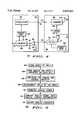
- FIG. 5is a flow chart 100 of a method for establishing a feedback loop for use with the programmable analog array 10 of FIG. 1.
- a programmable analog arrayis formed on a single semiconductor integrated circuit chip.
- the programmable analog arraycomprises an input/output circuit and an array of cells.
- the cellsare arranged in rows and columns.
- Analog circuitry and digital circuitryare formed in each cell of the array (step 104).
- the cells in the array of the programmable analog arrayare not limited to being identical to each other in the present invention.
- the programmable analog arraymay include cells with structures different from one another.
- the analog circuitry and the digital circuitryare not limited to being formed in the same cell in the programmable analog array.
- the analog circuitry and the digital circuitrycan be formed in alternate cells in the programmable analog array.
- a switch circuit in each cellconfigures the analog circuitry and the digital circuitry in accordance with the cell configuration data stored in a storage element such as a RAM.
- a storage elementsuch as a RAM.
- These cell configuration dataare continuously read to maintain the circuit configuration and component values of the analog circuitry and digital circuitry in the cells.
- the cell configuration data stored in the RAMcan be reconfigured from an external source in order to implement new circuits within the array of cells for new functional applications.
- the cell configuration dataare accessed to configure the analog circuitry and the digital circuitry of the cells using, for example, two programming shift registers and a control circuit.
- One programming shift registerprovides a row coordinate reference signal
- the other programming shift registerprovides a column coordinate reference signal.
- the row and column coordinate reference signalspermit individually accessing and configuring each cell in the programmable analog array.
- step 108interconnection between different cells in the array is established through interconnection circuitry in accordance with interconnection data stored in the RAM.
- the configuration of each cell in the array and the interconnection among different cells in the arraydetermine the functional applications of the programmable analog array.
- the analog circuitry and the digital circuitryform a digital feedback loop.
- the analog circuitrygenerates an analog signal (step 112), which is transmitted to the digital circuitry.
- the digital circuitryconverts the received analog signal into digital control information (step 114).
- the digital control informationis then used to adjust the analog circuitry by reconfiguring the variable connections and/or varying the component values of the analog circuitry (step 116). It should be understood that the analog circuitry in one cell in the array is not limited to being adjusted by the digital circuitry of the same cell in the present invention.
- a digital feedback loopmay be formed among two or more cells in the programmable analog array.
- the programable analog arrayincludes an array of cells. Each cell includes analog circuitry and digital circuitry. After the cells are configured and interconnected with one another to implement a functional application, the digital circuitry converts an analog signal received from the analog circuitry into digital control information, which is then used to adjust the analog circuitry. Because the feedback loop is established locally within one cell or among a few cells, the programable analog array in accordance with the present invention can be implemented with a minimum number of global data bus. Therefore, the present invention provides a semiconductor integrated circuit chip that is reliable, small in size, and cost efficient.
Landscapes
- Physics & Mathematics (AREA)
- Mathematical Physics (AREA)
- Engineering & Computer Science (AREA)
- Computer Hardware Design (AREA)
- Computing Systems (AREA)
- General Engineering & Computer Science (AREA)
- Logic Circuits (AREA)
- Design And Manufacture Of Integrated Circuits (AREA)
Abstract
Description
Claims (20)
Priority Applications (1)
| Application Number | Priority Date | Filing Date | Title |
|---|---|---|---|
| US08/586,503US5691664A (en) | 1996-01-16 | 1996-01-16 | Programmable analog array and method for establishing a feedback loop therein |
Applications Claiming Priority (1)
| Application Number | Priority Date | Filing Date | Title |
|---|---|---|---|
| US08/586,503US5691664A (en) | 1996-01-16 | 1996-01-16 | Programmable analog array and method for establishing a feedback loop therein |
Publications (1)
| Publication Number | Publication Date |
|---|---|
| US5691664Atrue US5691664A (en) | 1997-11-25 |
Family
ID=24346004
Family Applications (1)
| Application Number | Title | Priority Date | Filing Date |
|---|---|---|---|
| US08/586,503Expired - LifetimeUS5691664A (en) | 1996-01-16 | 1996-01-16 | Programmable analog array and method for establishing a feedback loop therein |
Country Status (1)
| Country | Link |
|---|---|
| US (1) | US5691664A (en) |
Cited By (56)
| Publication number | Priority date | Publication date | Assignee | Title |
|---|---|---|---|---|
| US5936469A (en)* | 1997-08-04 | 1999-08-10 | Motorola, Inc. | Amplifier with input referred common-mode adjustment |
| US5966047A (en)* | 1997-03-27 | 1999-10-12 | Motorola, Inc. | Programmable analog array and method |
| US6130842A (en)* | 1997-08-08 | 2000-10-10 | Cypress Semiconductor Corporation | Adjustable verify and program voltages in programmable devices |
| EP1170671A1 (en)* | 2000-07-04 | 2002-01-09 | STMicroelectronics S.r.l. | Programmable analog array circuit |
| US6763390B1 (en) | 2000-01-24 | 2004-07-13 | Ati Technologies, Inc. | Method and system for receiving and framing packetized data |
| US6778533B1 (en) | 2000-01-24 | 2004-08-17 | Ati Technologies, Inc. | Method and system for accessing packetized elementary stream data |
| US6785336B1 (en)* | 2000-01-24 | 2004-08-31 | Ati Technologies, Inc. | Method and system for retrieving adaptation field data associated with a transport packet |
| EP1202184A3 (en)* | 2000-10-26 | 2004-12-29 | Cypress Semiconductor Corporation | Programming methodology and architecture for an analog programmable system on a chip |
| US6885680B1 (en) | 2000-01-24 | 2005-04-26 | Ati International Srl | Method for synchronizing to a data stream |
| US6941336B1 (en) | 2000-10-26 | 2005-09-06 | Cypress Semiconductor Corporation | Programmable analog system architecture |
| US20050273284A1 (en)* | 2004-06-03 | 2005-12-08 | Pickerd John J | Flash array digitizer |
| US6988238B1 (en) | 2000-01-24 | 2006-01-17 | Ati Technologies, Inc. | Method and system for handling errors and a system for receiving packet stream data |
| US7113546B1 (en) | 2000-05-02 | 2006-09-26 | Ati Technologies, Inc. | System for handling compressed video data and method thereof |
| US20070009236A1 (en)* | 2000-11-06 | 2007-01-11 | Ati Technologies, Inc. | System for digital time shifting and method thereof |
| US7366961B1 (en) | 2000-01-24 | 2008-04-29 | Ati Technologies, Inc. | Method and system for handling errors |
| US20080307151A1 (en)* | 2006-04-03 | 2008-12-11 | Blaise Laurent Mouttet | Operational amplifier with resistance switch crossbar feedback |
| US7737724B2 (en) | 2007-04-17 | 2010-06-15 | Cypress Semiconductor Corporation | Universal digital block interconnection and channel routing |
| US7761845B1 (en) | 2002-09-09 | 2010-07-20 | Cypress Semiconductor Corporation | Method for parameterizing a user module |
| US7765095B1 (en) | 2000-10-26 | 2010-07-27 | Cypress Semiconductor Corporation | Conditional branching in an in-circuit emulation system |
| US7770113B1 (en) | 2001-11-19 | 2010-08-03 | Cypress Semiconductor Corporation | System and method for dynamically generating a configuration datasheet |
| US7774190B1 (en) | 2001-11-19 | 2010-08-10 | Cypress Semiconductor Corporation | Sleep and stall in an in-circuit emulation system |
| US7825688B1 (en) | 2000-10-26 | 2010-11-02 | Cypress Semiconductor Corporation | Programmable microcontroller architecture(mixed analog/digital) |
| US7844437B1 (en) | 2001-11-19 | 2010-11-30 | Cypress Semiconductor Corporation | System and method for performing next placements and pruning of disallowed placements for programming an integrated circuit |
| US7893724B2 (en) | 2004-03-25 | 2011-02-22 | Cypress Semiconductor Corporation | Method and circuit for rapid alignment of signals |
| US8026739B2 (en) | 2007-04-17 | 2011-09-27 | Cypress Semiconductor Corporation | System level interconnect with programmable switching |
| US8040266B2 (en) | 2007-04-17 | 2011-10-18 | Cypress Semiconductor Corporation | Programmable sigma-delta analog-to-digital converter |
| US8049569B1 (en) | 2007-09-05 | 2011-11-01 | Cypress Semiconductor Corporation | Circuit and method for improving the accuracy of a crystal-less oscillator having dual-frequency modes |
| US8069405B1 (en) | 2001-11-19 | 2011-11-29 | Cypress Semiconductor Corporation | User interface for efficiently browsing an electronic document using data-driven tabs |
| US8069436B2 (en) | 2004-08-13 | 2011-11-29 | Cypress Semiconductor Corporation | Providing hardware independence to automate code generation of processing device firmware |
| US8069428B1 (en) | 2001-10-24 | 2011-11-29 | Cypress Semiconductor Corporation | Techniques for generating microcontroller configuration information |
| US8067948B2 (en) | 2006-03-27 | 2011-11-29 | Cypress Semiconductor Corporation | Input/output multiplexer bus |
| US8078894B1 (en) | 2007-04-25 | 2011-12-13 | Cypress Semiconductor Corporation | Power management architecture, method and configuration system |
| US8078970B1 (en) | 2001-11-09 | 2011-12-13 | Cypress Semiconductor Corporation | Graphical user interface with user-selectable list-box |
| US8085100B2 (en) | 2005-02-04 | 2011-12-27 | Cypress Semiconductor Corporation | Poly-phase frequency synthesis oscillator |
| US8085067B1 (en) | 2005-12-21 | 2011-12-27 | Cypress Semiconductor Corporation | Differential-to-single ended signal converter circuit and method |
| US8089461B2 (en) | 2005-06-23 | 2012-01-03 | Cypress Semiconductor Corporation | Touch wake for electronic devices |
| US8092083B2 (en) | 2007-04-17 | 2012-01-10 | Cypress Semiconductor Corporation | Temperature sensor with digital bandgap |
| US8103497B1 (en) | 2002-03-28 | 2012-01-24 | Cypress Semiconductor Corporation | External interface for event architecture |
| US8103496B1 (en) | 2000-10-26 | 2012-01-24 | Cypress Semicondutor Corporation | Breakpoint control in an in-circuit emulation system |
| US8120408B1 (en) | 2005-05-05 | 2012-02-21 | Cypress Semiconductor Corporation | Voltage controlled oscillator delay cell and method |
| US8130025B2 (en) | 2007-04-17 | 2012-03-06 | Cypress Semiconductor Corporation | Numerical band gap |
| US8149048B1 (en) | 2000-10-26 | 2012-04-03 | Cypress Semiconductor Corporation | Apparatus and method for programmable power management in a programmable analog circuit block |
| US8160864B1 (en) | 2000-10-26 | 2012-04-17 | Cypress Semiconductor Corporation | In-circuit emulator and pod synchronized boot |
| US8176296B2 (en) | 2000-10-26 | 2012-05-08 | Cypress Semiconductor Corporation | Programmable microcontroller architecture |
| US8284845B1 (en) | 2000-01-24 | 2012-10-09 | Ati Technologies Ulc | Method and system for handling data |
| US8286125B2 (en) | 2004-08-13 | 2012-10-09 | Cypress Semiconductor Corporation | Model for a hardware device-independent method of defining embedded firmware for programmable systems |
| US8402313B1 (en) | 2002-05-01 | 2013-03-19 | Cypress Semiconductor Corporation | Reconfigurable testing system and method |
| US8499270B1 (en) | 2007-04-25 | 2013-07-30 | Cypress Semiconductor Corporation | Configuration of programmable IC design elements |
| US8516025B2 (en) | 2007-04-17 | 2013-08-20 | Cypress Semiconductor Corporation | Clock driven dynamic datapath chaining |
| US8533677B1 (en) | 2001-11-19 | 2013-09-10 | Cypress Semiconductor Corporation | Graphical user interface for dynamically reconfiguring a programmable device |
| EP2634710A4 (en)* | 2010-10-27 | 2014-10-22 | Zte Corp | Terminal device and method for realizing analog circuit in terminal device |
| US9448964B2 (en) | 2009-05-04 | 2016-09-20 | Cypress Semiconductor Corporation | Autonomous control in a programmable system |
| US9564902B2 (en) | 2007-04-17 | 2017-02-07 | Cypress Semiconductor Corporation | Dynamically configurable and re-configurable data path |
| US9720805B1 (en) | 2007-04-25 | 2017-08-01 | Cypress Semiconductor Corporation | System and method for controlling a target device |
| US10698662B2 (en) | 2001-11-15 | 2020-06-30 | Cypress Semiconductor Corporation | System providing automatic source code generation for personalization and parameterization of user modules |
| US20220139491A1 (en)* | 2018-12-21 | 2022-05-05 | Stmicroelectronics (Rousset) Sas | Electronic chip memory |
Citations (4)
| Publication number | Priority date | Publication date | Assignee | Title |
|---|---|---|---|---|
| JPS61101050A (en)* | 1984-10-24 | 1986-05-19 | Nec Corp | Standard cell system analogue integrated circuit |
| US4642487A (en)* | 1984-09-26 | 1987-02-10 | Xilinx, Inc. | Special interconnect for configurable logic array |
| US5055710A (en)* | 1986-12-26 | 1991-10-08 | Hitachi, Ltd. | Integrated logic circuit having plural input cells and flip-flop and output cells arranged in a cell block |
| US5196740A (en)* | 1990-04-03 | 1993-03-23 | Pilkington Micro-Electronics Limited | Integrated circuit for analogue system |
- 1996
- 1996-01-16USUS08/586,503patent/US5691664A/ennot_activeExpired - Lifetime
Patent Citations (4)
| Publication number | Priority date | Publication date | Assignee | Title |
|---|---|---|---|---|
| US4642487A (en)* | 1984-09-26 | 1987-02-10 | Xilinx, Inc. | Special interconnect for configurable logic array |
| JPS61101050A (en)* | 1984-10-24 | 1986-05-19 | Nec Corp | Standard cell system analogue integrated circuit |
| US5055710A (en)* | 1986-12-26 | 1991-10-08 | Hitachi, Ltd. | Integrated logic circuit having plural input cells and flip-flop and output cells arranged in a cell block |
| US5196740A (en)* | 1990-04-03 | 1993-03-23 | Pilkington Micro-Electronics Limited | Integrated circuit for analogue system |
Cited By (80)
| Publication number | Priority date | Publication date | Assignee | Title |
|---|---|---|---|---|
| US5966047A (en)* | 1997-03-27 | 1999-10-12 | Motorola, Inc. | Programmable analog array and method |
| US5936469A (en)* | 1997-08-04 | 1999-08-10 | Motorola, Inc. | Amplifier with input referred common-mode adjustment |
| US6130842A (en)* | 1997-08-08 | 2000-10-10 | Cypress Semiconductor Corporation | Adjustable verify and program voltages in programmable devices |
| US20050021813A1 (en)* | 2000-01-24 | 2005-01-27 | Ati Technologies, Inc. | Method and system for receiving and framing packetized data |
| US6763390B1 (en) | 2000-01-24 | 2004-07-13 | Ati Technologies, Inc. | Method and system for receiving and framing packetized data |
| US6778533B1 (en) | 2000-01-24 | 2004-08-17 | Ati Technologies, Inc. | Method and system for accessing packetized elementary stream data |
| US6785336B1 (en)* | 2000-01-24 | 2004-08-31 | Ati Technologies, Inc. | Method and system for retrieving adaptation field data associated with a transport packet |
| US8284845B1 (en) | 2000-01-24 | 2012-10-09 | Ati Technologies Ulc | Method and system for handling data |
| US6885680B1 (en) | 2000-01-24 | 2005-04-26 | Ati International Srl | Method for synchronizing to a data stream |
| US7376692B2 (en) | 2000-01-24 | 2008-05-20 | Ati Technologies, Inc. | Method and system for receiving and framing packetized data |
| US6988238B1 (en) | 2000-01-24 | 2006-01-17 | Ati Technologies, Inc. | Method and system for handling errors and a system for receiving packet stream data |
| US7366961B1 (en) | 2000-01-24 | 2008-04-29 | Ati Technologies, Inc. | Method and system for handling errors |
| US7113546B1 (en) | 2000-05-02 | 2006-09-26 | Ati Technologies, Inc. | System for handling compressed video data and method thereof |
| US6748370B2 (en) | 2000-07-04 | 2004-06-08 | Stmicroelectronics S.R.L. | Integrated cellular network structure that is programmable for solving differential equations |
| EP1170671A1 (en)* | 2000-07-04 | 2002-01-09 | STMicroelectronics S.r.l. | Programmable analog array circuit |
| US8103496B1 (en) | 2000-10-26 | 2012-01-24 | Cypress Semicondutor Corporation | Breakpoint control in an in-circuit emulation system |
| US9843327B1 (en) | 2000-10-26 | 2017-12-12 | Cypress Semiconductor Corporation | PSOC architecture |
| US8555032B2 (en) | 2000-10-26 | 2013-10-08 | Cypress Semiconductor Corporation | Microcontroller programmable system on a chip with programmable interconnect |
| US8736303B2 (en) | 2000-10-26 | 2014-05-27 | Cypress Semiconductor Corporation | PSOC architecture |
| US10725954B2 (en) | 2000-10-26 | 2020-07-28 | Monterey Research, Llc | Microcontroller programmable system on a chip |
| US8358150B1 (en) | 2000-10-26 | 2013-01-22 | Cypress Semiconductor Corporation | Programmable microcontroller architecture(mixed analog/digital) |
| EP1202184A3 (en)* | 2000-10-26 | 2004-12-29 | Cypress Semiconductor Corporation | Programming methodology and architecture for an analog programmable system on a chip |
| US8176296B2 (en) | 2000-10-26 | 2012-05-08 | Cypress Semiconductor Corporation | Programmable microcontroller architecture |
| US7765095B1 (en) | 2000-10-26 | 2010-07-27 | Cypress Semiconductor Corporation | Conditional branching in an in-circuit emulation system |
| US8160864B1 (en) | 2000-10-26 | 2012-04-17 | Cypress Semiconductor Corporation | In-circuit emulator and pod synchronized boot |
| US8149048B1 (en) | 2000-10-26 | 2012-04-03 | Cypress Semiconductor Corporation | Apparatus and method for programmable power management in a programmable analog circuit block |
| US7825688B1 (en) | 2000-10-26 | 2010-11-02 | Cypress Semiconductor Corporation | Programmable microcontroller architecture(mixed analog/digital) |
| US9766650B2 (en) | 2000-10-26 | 2017-09-19 | Cypress Semiconductor Corporation | Microcontroller programmable system on a chip with programmable interconnect |
| US6941336B1 (en) | 2000-10-26 | 2005-09-06 | Cypress Semiconductor Corporation | Programmable analog system architecture |
| US10261932B2 (en) | 2000-10-26 | 2019-04-16 | Cypress Semiconductor Corporation | Microcontroller programmable system on a chip |
| US10248604B2 (en) | 2000-10-26 | 2019-04-02 | Cypress Semiconductor Corporation | Microcontroller programmable system on a chip |
| US10020810B2 (en) | 2000-10-26 | 2018-07-10 | Cypress Semiconductor Corporation | PSoC architecture |
| USRE47054E1 (en) | 2000-11-06 | 2018-09-18 | Ati Technologies Ulc | System for digital time shifting and method thereof |
| US20070009236A1 (en)* | 2000-11-06 | 2007-01-11 | Ati Technologies, Inc. | System for digital time shifting and method thereof |
| US8260109B2 (en) | 2000-11-06 | 2012-09-04 | Ati Technologies Ulc | System for digital time shifting and method thereof |
| US8793635B1 (en) | 2001-10-24 | 2014-07-29 | Cypress Semiconductor Corporation | Techniques for generating microcontroller configuration information |
| US8069428B1 (en) | 2001-10-24 | 2011-11-29 | Cypress Semiconductor Corporation | Techniques for generating microcontroller configuration information |
| US10466980B2 (en) | 2001-10-24 | 2019-11-05 | Cypress Semiconductor Corporation | Techniques for generating microcontroller configuration information |
| US8078970B1 (en) | 2001-11-09 | 2011-12-13 | Cypress Semiconductor Corporation | Graphical user interface with user-selectable list-box |
| US10698662B2 (en) | 2001-11-15 | 2020-06-30 | Cypress Semiconductor Corporation | System providing automatic source code generation for personalization and parameterization of user modules |
| US7770113B1 (en) | 2001-11-19 | 2010-08-03 | Cypress Semiconductor Corporation | System and method for dynamically generating a configuration datasheet |
| US7844437B1 (en) | 2001-11-19 | 2010-11-30 | Cypress Semiconductor Corporation | System and method for performing next placements and pruning of disallowed placements for programming an integrated circuit |
| US8533677B1 (en) | 2001-11-19 | 2013-09-10 | Cypress Semiconductor Corporation | Graphical user interface for dynamically reconfiguring a programmable device |
| US8370791B2 (en) | 2001-11-19 | 2013-02-05 | Cypress Semiconductor Corporation | System and method for performing next placements and pruning of disallowed placements for programming an integrated circuit |
| US8069405B1 (en) | 2001-11-19 | 2011-11-29 | Cypress Semiconductor Corporation | User interface for efficiently browsing an electronic document using data-driven tabs |
| US7774190B1 (en) | 2001-11-19 | 2010-08-10 | Cypress Semiconductor Corporation | Sleep and stall in an in-circuit emulation system |
| US8103497B1 (en) | 2002-03-28 | 2012-01-24 | Cypress Semiconductor Corporation | External interface for event architecture |
| US8402313B1 (en) | 2002-05-01 | 2013-03-19 | Cypress Semiconductor Corporation | Reconfigurable testing system and method |
| US7761845B1 (en) | 2002-09-09 | 2010-07-20 | Cypress Semiconductor Corporation | Method for parameterizing a user module |
| US7893724B2 (en) | 2004-03-25 | 2011-02-22 | Cypress Semiconductor Corporation | Method and circuit for rapid alignment of signals |
| US7098839B2 (en)* | 2004-06-03 | 2006-08-29 | Tektronix, Inc. | Flash array digitizer |
| US20050273284A1 (en)* | 2004-06-03 | 2005-12-08 | Pickerd John J | Flash array digitizer |
| US8286125B2 (en) | 2004-08-13 | 2012-10-09 | Cypress Semiconductor Corporation | Model for a hardware device-independent method of defining embedded firmware for programmable systems |
| US8069436B2 (en) | 2004-08-13 | 2011-11-29 | Cypress Semiconductor Corporation | Providing hardware independence to automate code generation of processing device firmware |
| US8085100B2 (en) | 2005-02-04 | 2011-12-27 | Cypress Semiconductor Corporation | Poly-phase frequency synthesis oscillator |
| US8120408B1 (en) | 2005-05-05 | 2012-02-21 | Cypress Semiconductor Corporation | Voltage controlled oscillator delay cell and method |
| US8089461B2 (en) | 2005-06-23 | 2012-01-03 | Cypress Semiconductor Corporation | Touch wake for electronic devices |
| US8085067B1 (en) | 2005-12-21 | 2011-12-27 | Cypress Semiconductor Corporation | Differential-to-single ended signal converter circuit and method |
| US8067948B2 (en) | 2006-03-27 | 2011-11-29 | Cypress Semiconductor Corporation | Input/output multiplexer bus |
| US8717042B1 (en) | 2006-03-27 | 2014-05-06 | Cypress Semiconductor Corporation | Input/output multiplexer bus |
| US20080307151A1 (en)* | 2006-04-03 | 2008-12-11 | Blaise Laurent Mouttet | Operational amplifier with resistance switch crossbar feedback |
| US7755424B2 (en) | 2006-04-03 | 2010-07-13 | Blaise Laurent Mouttet | Operational amplifier with resistance switch crossbar feedback |
| US8040266B2 (en) | 2007-04-17 | 2011-10-18 | Cypress Semiconductor Corporation | Programmable sigma-delta analog-to-digital converter |
| US8476928B1 (en) | 2007-04-17 | 2013-07-02 | Cypress Semiconductor Corporation | System level interconnect with programmable switching |
| US7737724B2 (en) | 2007-04-17 | 2010-06-15 | Cypress Semiconductor Corporation | Universal digital block interconnection and channel routing |
| US8482313B2 (en) | 2007-04-17 | 2013-07-09 | Cypress Semiconductor Corporation | Universal digital block interconnection and channel routing |
| US8026739B2 (en) | 2007-04-17 | 2011-09-27 | Cypress Semiconductor Corporation | System level interconnect with programmable switching |
| US9564902B2 (en) | 2007-04-17 | 2017-02-07 | Cypress Semiconductor Corporation | Dynamically configurable and re-configurable data path |
| US8516025B2 (en) | 2007-04-17 | 2013-08-20 | Cypress Semiconductor Corporation | Clock driven dynamic datapath chaining |
| US8092083B2 (en) | 2007-04-17 | 2012-01-10 | Cypress Semiconductor Corporation | Temperature sensor with digital bandgap |
| US8130025B2 (en) | 2007-04-17 | 2012-03-06 | Cypress Semiconductor Corporation | Numerical band gap |
| US8078894B1 (en) | 2007-04-25 | 2011-12-13 | Cypress Semiconductor Corporation | Power management architecture, method and configuration system |
| US9720805B1 (en) | 2007-04-25 | 2017-08-01 | Cypress Semiconductor Corporation | System and method for controlling a target device |
| US8909960B1 (en) | 2007-04-25 | 2014-12-09 | Cypress Semiconductor Corporation | Power management architecture, method and configuration system |
| US8499270B1 (en) | 2007-04-25 | 2013-07-30 | Cypress Semiconductor Corporation | Configuration of programmable IC design elements |
| US8049569B1 (en) | 2007-09-05 | 2011-11-01 | Cypress Semiconductor Corporation | Circuit and method for improving the accuracy of a crystal-less oscillator having dual-frequency modes |
| US9448964B2 (en) | 2009-05-04 | 2016-09-20 | Cypress Semiconductor Corporation | Autonomous control in a programmable system |
| EP2634710A4 (en)* | 2010-10-27 | 2014-10-22 | Zte Corp | Terminal device and method for realizing analog circuit in terminal device |
| US20220139491A1 (en)* | 2018-12-21 | 2022-05-05 | Stmicroelectronics (Rousset) Sas | Electronic chip memory |
| US11621051B2 (en)* | 2018-12-21 | 2023-04-04 | Stmicroelectronics Sa | Electronic chip memory |
Similar Documents
| Publication | Publication Date | Title |
|---|---|---|
| US5691664A (en) | Programmable analog array and method for establishing a feedback loop therein | |
| US5680070A (en) | Programmable analog array and method for configuring the same | |
| US9843327B1 (en) | PSOC architecture | |
| EP0797870B1 (en) | Cmos voltage-controlled oscillator having a wide frequency range | |
| US5847617A (en) | Variable-path-length voltage-controlled oscillator circuit | |
| US7550994B1 (en) | Programmable logic device with on-chip nonvolatile user memory | |
| US6218876B1 (en) | Phase-locked loop circuitry for programmable logic devices | |
| US6870411B2 (en) | Phase synchronizing circuit | |
| US5699003A (en) | Delay circuit device | |
| US6512395B1 (en) | Configurable memory for programmable logic circuits | |
| US6806733B1 (en) | Multiple data rate interface architecture | |
| US6954091B2 (en) | Programmable phase-locked loop | |
| US5608345A (en) | Programmable switched capacitor circuit | |
| US8098082B1 (en) | Multiple data rate interface architecture | |
| US7973563B2 (en) | Programmable IO architecture | |
| US5075575A (en) | Externally synchronized programmable device | |
| WO1995032481A1 (en) | Integrated circuit having programmable analog modules with configurable interconnects between them | |
| JP2006311561A (en) | Circuit, oscillator, ring oscillator and method for generating multiple oscillation signals | |
| JP3928666B2 (en) | Clock signal distribution and synchronization in digital systems | |
| US6310523B1 (en) | Wide-range and low-power consumption voltage-controlled oscillator | |
| KR19980082198A (en) | Semiconductor device and its power-on reset circuit | |
| CA2053322C (en) | Integrated circuit and gate array | |
| JP2001285056A (en) | Automatic trimming circuit for oscillator | |
| EP0177280B1 (en) | Dynamically controllable output logic circuit | |
| US6842082B2 (en) | Programmable voltage-controlled oscillator with self-calibration feature |
Legal Events
| Date | Code | Title | Description |
|---|---|---|---|
| AS | Assignment | Owner name:MOTOROLA, INC., ILLINOIS Free format text:ASSIGNMENT OF ASSIGNORS INTEREST;ASSIGNORS:ANDERSON, DAVID J.;BERSCH, DANNY A.;REEL/FRAME:007843/0569 Effective date:19951228 | |
| STCF | Information on status: patent grant | Free format text:PATENTED CASE | |
| FEPP | Fee payment procedure | Free format text:PAYOR NUMBER ASSIGNED (ORIGINAL EVENT CODE: ASPN); ENTITY STATUS OF PATENT OWNER: LARGE ENTITY | |
| AS | Assignment | Owner name:ANADIGM LIMITED, UNITED KINGDOM Free format text:ASSIGNMENT OF ASSIGNORS INTEREST;ASSIGNORS:MOTOROLA LIMITED;MOTOROLA INC.;REEL/FRAME:011648/0267 Effective date:20010223 | |
| FPAY | Fee payment | Year of fee payment:4 | |
| AS | Assignment | Owner name:GATX EUROPEAN TECHNOLOGY VENTURES, ENGLAND Free format text:SECURITY AGREEMENT;ASSIGNOR:ANADIGM LIMITED;REEL/FRAME:012665/0383 Effective date:20020430 | |
| AS | Assignment | Owner name:ANADIGM LIMITED, GREAT BRITAIN Free format text:ASSIGNMENT OF ASSIGNORS INTEREST;ASSIGNOR:MOTOROLA, INC.;REEL/FRAME:013295/0492 Effective date:20020228 | |
| FPAY | Fee payment | Year of fee payment:8 | |
| AS | Assignment | Owner name:ETV CAPITAL SA, LUXEMBOURG Free format text:NUNC PRO TUNC ASSIGNMENT;ASSIGNOR:GATX EUROPEAN TECHNOLOGY VENTURES;REEL/FRAME:020288/0108 Effective date:20071220 | |
| AS | Assignment | Owner name:NEW ANADIGM, CALIFORNIA Free format text:NUNC PRO TUNC ASSIGNMENT;ASSIGNOR:ETV CAPITAL SA;REEL/FRAME:020317/0953 Effective date:20080107 | |
| AS | Assignment | Owner name:NEADIWA SOFTWARE KR, L.L.C., DELAWARE Free format text:ASSIGNMENT OF ASSIGNORS INTEREST;ASSIGNOR:ANADIGM LIMITED;REEL/FRAME:021817/0858 Effective date:20080918 | |
| FPAY | Fee payment | Year of fee payment:12 |