US5691541A - Maskless, reticle-free, lithography - Google Patents
Maskless, reticle-free, lithographyDownload PDFInfo
- Publication number
- US5691541A US5691541AUS08/645,531US64553196AUS5691541AUS 5691541 AUS5691541 AUS 5691541AUS 64553196 AUS64553196 AUS 64553196AUS 5691541 AUS5691541 AUS 5691541A
- Authority
- US
- United States
- Prior art keywords
- array
- programmable array
- substrate
- lithography system
- image
- Prior art date
- Legal status (The legal status is an assumption and is not a legal conclusion. Google has not performed a legal analysis and makes no representation as to the accuracy of the status listed.)
- Expired - Lifetime
Links
Images


Classifications
- G—PHYSICS
- G03—PHOTOGRAPHY; CINEMATOGRAPHY; ANALOGOUS TECHNIQUES USING WAVES OTHER THAN OPTICAL WAVES; ELECTROGRAPHY; HOLOGRAPHY
- G03F—PHOTOMECHANICAL PRODUCTION OF TEXTURED OR PATTERNED SURFACES, e.g. FOR PRINTING, FOR PROCESSING OF SEMICONDUCTOR DEVICES; MATERIALS THEREFOR; ORIGINALS THEREFOR; APPARATUS SPECIALLY ADAPTED THEREFOR
- G03F7/00—Photomechanical, e.g. photolithographic, production of textured or patterned surfaces, e.g. printing surfaces; Materials therefor, e.g. comprising photoresists; Apparatus specially adapted therefor
- G03F7/70—Microphotolithographic exposure; Apparatus therefor
- G03F7/70691—Handling of masks or workpieces
- G03F7/70791—Large workpieces, e.g. glass substrates for flat panel displays or solar panels
- G—PHYSICS
- G03—PHOTOGRAPHY; CINEMATOGRAPHY; ANALOGOUS TECHNIQUES USING WAVES OTHER THAN OPTICAL WAVES; ELECTROGRAPHY; HOLOGRAPHY
- G03F—PHOTOMECHANICAL PRODUCTION OF TEXTURED OR PATTERNED SURFACES, e.g. FOR PRINTING, FOR PROCESSING OF SEMICONDUCTOR DEVICES; MATERIALS THEREFOR; ORIGINALS THEREFOR; APPARATUS SPECIALLY ADAPTED THEREFOR
- G03F7/00—Photomechanical, e.g. photolithographic, production of textured or patterned surfaces, e.g. printing surfaces; Materials therefor, e.g. comprising photoresists; Apparatus specially adapted therefor
- G03F7/70—Microphotolithographic exposure; Apparatus therefor
- G03F7/70008—Production of exposure light, i.e. light sources
- G03F7/70041—Production of exposure light, i.e. light sources by pulsed sources, e.g. multiplexing, pulse duration, interval control or intensity control
- G—PHYSICS
- G03—PHOTOGRAPHY; CINEMATOGRAPHY; ANALOGOUS TECHNIQUES USING WAVES OTHER THAN OPTICAL WAVES; ELECTROGRAPHY; HOLOGRAPHY
- G03F—PHOTOMECHANICAL PRODUCTION OF TEXTURED OR PATTERNED SURFACES, e.g. FOR PRINTING, FOR PROCESSING OF SEMICONDUCTOR DEVICES; MATERIALS THEREFOR; ORIGINALS THEREFOR; APPARATUS SPECIALLY ADAPTED THEREFOR
- G03F7/00—Photomechanical, e.g. photolithographic, production of textured or patterned surfaces, e.g. printing surfaces; Materials therefor, e.g. comprising photoresists; Apparatus specially adapted therefor
- G03F7/70—Microphotolithographic exposure; Apparatus therefor
- G03F7/70216—Mask projection systems
- G03F7/70283—Mask effects on the imaging process
- G03F7/70291—Addressable masks, e.g. spatial light modulators [SLMs], digital micro-mirror devices [DMDs] or liquid crystal display [LCD] patterning devices
- G—PHYSICS
- G03—PHOTOGRAPHY; CINEMATOGRAPHY; ANALOGOUS TECHNIQUES USING WAVES OTHER THAN OPTICAL WAVES; ELECTROGRAPHY; HOLOGRAPHY
- G03F—PHOTOMECHANICAL PRODUCTION OF TEXTURED OR PATTERNED SURFACES, e.g. FOR PRINTING, FOR PROCESSING OF SEMICONDUCTOR DEVICES; MATERIALS THEREFOR; ORIGINALS THEREFOR; APPARATUS SPECIALLY ADAPTED THEREFOR
- G03F7/00—Photomechanical, e.g. photolithographic, production of textured or patterned surfaces, e.g. printing surfaces; Materials therefor, e.g. comprising photoresists; Apparatus specially adapted therefor
- G03F7/70—Microphotolithographic exposure; Apparatus therefor
- G03F7/70425—Imaging strategies, e.g. for increasing throughput or resolution, printing product fields larger than the image field or compensating lithography- or non-lithography errors, e.g. proximity correction, mix-and-match, stitching or double patterning
- G03F7/70475—Stitching, i.e. connecting image fields to produce a device field, the field occupied by a device such as a memory chip, processor chip, CCD, flat panel display
- G—PHYSICS
- G03—PHOTOGRAPHY; CINEMATOGRAPHY; ANALOGOUS TECHNIQUES USING WAVES OTHER THAN OPTICAL WAVES; ELECTROGRAPHY; HOLOGRAPHY
- G03F—PHOTOMECHANICAL PRODUCTION OF TEXTURED OR PATTERNED SURFACES, e.g. FOR PRINTING, FOR PROCESSING OF SEMICONDUCTOR DEVICES; MATERIALS THEREFOR; ORIGINALS THEREFOR; APPARATUS SPECIALLY ADAPTED THEREFOR
- G03F7/00—Photomechanical, e.g. photolithographic, production of textured or patterned surfaces, e.g. printing surfaces; Materials therefor, e.g. comprising photoresists; Apparatus specially adapted therefor
- G03F7/70—Microphotolithographic exposure; Apparatus therefor
- G03F7/70691—Handling of masks or workpieces
- G03F7/70716—Stages
- G03F7/70725—Stages control
Definitions
- the inventionrelates to the field of projection lithography in which a pattern is printed onto a substrate such as a wafer, a flat panel or a circuit board.
- the lithographic production of integrated circuits, flat panel displays, magnetic head structures and other micro-mechanical devicesgenerally involves the use of optical steppers to image a master pattern contained on a mask or reticle through a lens onto a wafer or glass substrate using visible or ultraviolet light.
- the field size of the imaging lensis generally much smaller than the full area to be patterned on the substrate, so either multiple exposures are made using a step-and-repeat motion of the stage in the image plane, or the reticle and image plane stage are scanned in synchronism to expose an area which is bigger than that covered by the lens.
- the former systemis often called a step-and-repeat system, and the latter a scanner or a step-and-scan system.
- the mask or reticleIn both classes of lithography system the mask or reticle is an expensive element which takes time to write, inspect, repair and protect. Any time a modification of the reticle pattern is required, no matter how trivial the change, a new reticle must be prepared which takes time and costs money. Changing the reticle is generally a slow process, so if multiple reticles are required to expose the same substrate or if only a few substrates are required for each reticle pattern, then the throughput of the lithography system suffers substantially.
- mask and reticleare used interchangeably herein. Both represent the carrier for the master pattern to be replicated in a projection lithography system.
- maskis used when the projection optics have a magnification factor of unity and the pattern on the mask comprises the totality of the information to be transferred onto the wafer.
- reticleis used when the pattern of the reticle comprises a subset of the information to be transferred to the wafer.
- the inventionbasically includes a pulsed or strobed radiation source with illumination optics to produce an illumination beam made up of a sequence of radiation pulses, a programmable array of binary light switches which is illuminated by the pulses of the illumination beam and which is controllably configured to reflect or diffract a desired pattern of radiation from each pulse, and a projection system which projects the desired pattern of radiation onto a substrate.
- the substrateis mounted on a scanning substrate stage that is in motion during the sequence of pulses but which moves only a small fraction of a minimum feature size during the time of a single pulse.
- the present inventionobviates many limitations of reticle/mask based lithography, because the master pattern data is no longer resident on a specific carrier such as a piece of glass. Instead it is resident in a computer memory where it can be quickly accessed, and if necessary, easily modified. Multiple, identical copies of the pattern can be readily transferred to multiple lithography systems.
- the master pattern datais transferred to a programmable array of binary light switches located in the object plane of a projection system.
- a preferred programmable arrayis the digital micro-mirror device (DMD) by Texas Instruments (TI).
- DMDdigital micro-mirror device
- TITexas Instruments
- the array of mirrorsserves as a programmable array of binary light switches, a deflected mirror corresponding to a dark portion of a desired pattern, and an undeflected mirror corresponding to a bright portion of the pattern or vice versa.
- a high contrast patterncan thus be projected onto a substrate each time the illumination source flashes.
- Programmable array devicesbased on arrays of mirrors, and also based on gratings and interference effects can also be used.
- Programmable arrayscan be used with a variety of radiation sources, including visible light, ultraviolet light, extreme ultraviolet (EUV), x-rays, electrons and ions.
- the pulsed or strobed sourcemay be formed of an emitter which operates in a pulsed mode or a continuous emitter with a shutter or other strobe means located anywhere in the optical system to produce a pulsed illumination beam.
- Maskless, reticle-free lithographycan introduce redundancy into the pattern replication process and thereby obviate the need for defect free programmable arrays. This is done by using multiple flashes or pulses to achieve a full exposure and many array pixels to make up a single minimum feature on the exposed wafer.
- the maskless lithographic schemecan be very forgiving of an inoperative pixel in the programmable array.
- a large linear array of DMDscould be made to span the field length of a scanner lens.
- a continuous band of imagery across the length of the scanner lenscan be achieved by staggering the placement of the DMD arrays in the direction of scanning.
- Appropriate exposure continuity and uniformity at the plane of the substratecan be produced by an appropriate programming sequence for the array.
- the pulsed or strobed illumination systemmust have the appropriate spectral properties to complement the optical projection system.
- the travel of the wafer during the illumination pulsemust be short in comparison to the size of a minimum feature.
- a number of optical sourcescan be used with the DMD embodiment, including excimer lasers, and frequency multiplied, diode-pumped, solid state lasers and copper vapor lasers, all of which provide short wavelength illumination, pulsed at kilohertz or multi-kilohertz frequencies, and with pulse durations less than 100 nsec.
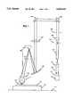
- FIG. 1is a schematic view of the principal components of a maskless optical lithography system.
- FIG. 2is a small section through a specific array of a digital micro-mirror device (DMD) showing small groups of mirrors in the on and off positions.
- DMDdigital micro-mirror device
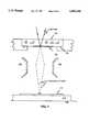
- FIG. 3shows a collection of programmable arrays constructed so that a continuous band of imagery is produced that spans the length of the field of the relay lens.
- FIG. 4shows a succession of four programmable array images employed to place the resultant edge of the image on the substrate with an accuracy that is a small fraction of an array pixel.
- FIG. 5shows the major subsystem components for a maskless optical lithography system, including control and data path details.
- FIG. 6shows the major subsystem components for a maskless electron beam lithography system.
- FIG. 7shows some of the major components in the electron imaging part of a maskless electron beam lithography system.
- the function of the mask or reticle used in prior art systemsis replaced by a programmable array which is illuminated by a pulsed or strobed light source and imaged onto a substrate which is being scanned at constant velocity. All the information to be projected onto the substrate is contained in the programmable array and may be readily changed by computer control of the array elements without changing any of the hardware in the system.
- a maskless lithography systemhas an illumination source 99 which produces, alone or in combination with other components as described herein, a pulsed illumination beam 100.
- beam 100can be the pulsed output beam from an excimer laser, which typically has a pulse duration of about 30 ns and which can be pulsed at rates that exceed 1000 Hz.
- This beamenters a relay system represented by relay lens 101 but which is typically an anamorphic system containing cylindrical lenses that create the desired numerical aperture in the beam before it is introduced into a light pipe 102 that will improve the spatial uniformity of the laser beam and define its area when it emerges.
- a fly's eye lens arraycould be used to perform the same function as the light pipe 102.
- a relay systemconsisting of two illuminator lenses 103, 107, two fold mirrors 105, 106, and a curved mirror 108, form a magnifying relay that images the output face of the light pipe 102 onto a programmable array 109 and images an illuminator pupil (stop) 104 at the projection lens pupil (stop) 110 when the light is simply reflected from the programmable array 109.
- the illuminator pupil 104is located in the magnifying relay system, after lens 103, and the projection lens pupil 110 is located before a projection lens 111, which can be a more complex projection system.
- the elements of the programmable array which are turned onact as a simple plane mirror and direct incident illumination into the projection lens pupil 110.
- a portion of a pattern stored in a computer memorycan be input into the programmable array and imaged with projection lens 111 onto a substrate 112 each time the light beam flashes.
- the substrate 112is mounted on a continuously moving stage 113 which is mounted on a platen 114.
- An electronic control systemcoordinates the changing of the image data in the programmable array between flashes or pulses and the triggering of each flash or pulse so that the resultant image has no underexposed gaps or overexposed overlaps.
- the time between flashes or pulsesmust exactly correspond to the time taken for a stage motion corresponding to the length of the programmable array in the scan direction or some integral fraction thereof.
- the light sourceneed not be a excimer laser. Any pulsed or strobed source of radiation including lasers, flash lamps and light emitting diodes might be used, so long as the radiation is compatible with the binary switching system of the programmable array and the projection optical system. Sources of visible or ultraviolet light which produce an exposing wavelength between 7000 ⁇ and 1200 ⁇ can be used.
- Sources of extreme ultraviolet (EUV) or soft x-ray radiation with a wavelength between 50 ⁇ and 200 ⁇can also be used.
- the programmable arraywould then be made of EUV or soft x-ray mirrors. Examples of such mirrors are (a) grazing incidence reflectors of the radiation and (b) multilayer resonant reflectors of the radiation.
- a grazing incidence reflectormay be a reflector element with a coating of high atomic number (Z) material selected from tungsten, gold, rubidium, platinum, titanium or other materials with Z greater than 12.
- a multilayer resonant reflectormay be a reflector element with multilayer coatings of Mo/Si, Mo/Be, W/C, Ru/B 4 C, or Ru/Si; other suitable combinations are shown in Hawryluk and Ceglio, "Wavelength considerations in soft x-ray projection lithography," Applied Optics, Vol. 32, No. 34, 1 Dec. 1993, pp. 7062-7067.
- the pulsed radiation sourcemay be a source which operates in a pulsed mode
- the sourcemay also be a continuous (CW) radiation emitter which is modulated or strobed by any suitable means, e.g. a high frequency shutter.
- CWcontinuous
- Separate shutter or other strobing meansmay be placed anywhere in the system, either before or after the array, e.g. at illustrative positions 115-118 in FIG. 1, or the elements of the array itself may act as a shutter.
- illuminationis provided by any pulsed illumination system with the appropriate spectral properties dictated by the optical projection system.
- a constraint on the pulsed illumination systemis that the wafer motion during the pulse must be short in comparison to the size of a minimum feature. Moving the substrate slowly is not desirable if maximum system throughput is to be achieved, and stopping the stage for each flash would not be time efficient either.
- a preferred embodiment of a programmable arrayis the digital micro-mirror device (DMD) currently manufactured by Texas Instruments (TI) as described in Mignardi, "Digital Micro-Mirror Array for Projection TV," Solid State Technology, July 1994, p. 63.
- DMDdigital micro-mirror device
- TITexas Instruments
- a single such DMD devicemay hold as many as 2 million mirrors with each mirror being about 16 ⁇ m square with a 17 ⁇ m center to center spacing.
- Each mirrorcan be independently deflected over a ⁇ 10 degree range of angular motion with a settling time of a few microseconds.
- the array of mirrorsserves as a programmable array of binary light switches wherein a deflected mirror corresponds to a dark portion of a desired pattern (switch off), and an undeflected mirror corresponds to a bright portion of the pattern (switch on).
- a high contrast patterncan be projected onto a substrate each time the illumination source flashes.
- the DMDis just one example of a programmable array of switches.
- Other programmable array devicesoperate with sources of lithographic radiation other than just visible or ultraviolet light. Such other sources of radiation include extreme ultraviolet (EUV), x-rays, and electrons and ions.
- Programmable arraysmay be based on arrays of mirrors, like the TI device, or on gratings or on interference effects to provide switching at each pixel location. With further development, microdevices such as the DMD will have more and smaller pixels and they will be much faster, thus expanding the capabilities of this technique.
- a number of optical sourcesare appropriate for use with the DMD embodiment.
- One illumination sourceis the excimer laser which typically flashes for about 30 ns and can be pulsed at rates up to 1000 Hz. With a stage velocity of 25 mm/sec, the distance traveled per flash is only about 6 ⁇ . There are other short pulse, high repetition rate lasers which also meet this requirement. Diode pumped solid state lasers and copper vapor lasers both can be frequency multiplied (i.e. wavelength reduced) to provide short wavelength illumination, and both can be operated at multi-kilohertz frequencies with pulse durations less than 100 ns.
- the DMD mirror arraycould be coated with multilayered resonant reflectors, as described above, for EUV or soft x-ray radiation. Then the multilayer coated DMD can serve as a programmable array for EUV or soft x-ray projection lithography.
- multilayered coatingsare Mo/Si coatings for narrowband radiation around 13.5 nm, and Mo/Be coatings for radiation around 11.5 nm.
- the DMD mirror arraycould be used to image light on a photocathode with an appropriate photoemissive material such as CsI, CeTe, SbCs, AgOCs, InGaAs, NaKSbCs, NaKSb, or GaAsP.
- the illuminated photocathodewould become an electron emitter serving as a programmable array for projection electron lithography.
- Whether a pixel element is turned on or offwill depend on the design of the programmable array and the way it is employed in the optical system. In the case of a mirror array type, it is possible to arrange the optics so that illumination striking a deflected mirror in the array is imaged on the substrate and light striking an undetected mirror in the array is dumped or vice versa.
- the programmable array or collection of arrayswill not fill the field of the projection system, but will utilize a strip stretching from one side of the field to the other, across the center of the field. It is also possible to employ a ring field type projection system and to arrange the programmable arrays so that they lie within the arcuate shape of the corrected field.
- FIG. 2is a small section through a specific array of the digital micro-mirror device (DMD) showing how a small group of mirrors may be deflected (switched off) to dump the incident energy out of the acceptance angle of the relay lens and how another group of mirrors may be left undetected (switched on) to reflect the incident illumination into the relay lens.
- DMDdigital micro-mirror device
- FIG. 2A small section of a programmable array 200, similar in principle to the DMDs produced by TI, is schematically illustrated in FIG. 2.
- Programmable array 200consists of individual addressable mirror elements 201 arranged in an array on a substrate 202. A portion of a pattern is contained in the array so that some of the elements are turned on (the horizontal mirror elements 201h) and some are turned off (the tilted mirror elements 201t).
- the "on" elements 201hreflect the incident illumination just as a plane mirror would. When used in the configuration shown in FIG. 1 this light would be directed into the pupil 110 of the projection system and would form the bright portion of the image.
- the light striking the tilted DMD array "off" elements 201tis reflected out of the pupil 110 of the projection system and would therefore comprise the dark portion of the image.
- the optimum magnification between the mirror array and the substratewill depend on the application, and on the type of programmable array used in the application.
- a currently available Texas Instruments DMDwhich has a 17 ⁇ m spacing between mirror elements, requires a magnification from the substrate to the array to be of order 17, so that each mirror in the programmable array is equivalent to about 1 ⁇ m on the image plane and approximately 9 mirrors are required to form a minimum feature of 3 ⁇ m by 3 ⁇ m.
- the number of programmable arrays required to span the field of a lithography systemwill depend on the application and the desired performance. For example if a 50 mm wide image field is desired for the flat panel application, and each DMD type array is 2000 mirror elements wide, then 25 DMDs are required to span the field. In the integrated circuit application requiring 0.5 ⁇ m minimum feature size, about 66 DMDs are required to span a 22 mm field.
- a collection of programmable arrayscan be constructed so that a continuous band of imagery is produced that spans the length of the field of the relay lens.
- the need to butt the arrays together to form a continuous band of imageryis avoided by staggering the placement of the individual arrays in the direction of scanning.
- the data handling systemtakes into account the discontinuities in the scanning direction so that a continuous image is produced on the substrate when the system is scanned.
- a continuous band of DMDsis produced by staggering the position of individual DMD packages 302 so that the edges 303 of the active element arrays 301 in the packages line up in the scan direction.
- the differences in scan positioncan be accommodated by the data handling system which simply delays inputting image data to DMDs which are scanned later than the others.
- FIG. 4shows a succession of 4 programmable array images, i.e. the light pattern projected by the array onto the resist. Each image corresponds to a different flash of the light source; the four images are averaged together by the resist to place the resultant edge of the image on the substrate with an accuracy that is a small fraction of an array pixel.
- a single exposurecan locate a line edge along any edge corresponding to a pixel or half way between two pixel edges by alternating on and off with every pixel along the desired edge. Since the pixels are below the resolution of the projection system, the rough edge produced by turning on every other pixel is smoothed and averaged by the projection system to a clean edge on the substrate half way between the boundaries of the alternating pixels.
- pixels 401a, care on but 401b, d are off; if one exposure were sufficient, then this would move edge 403 over a distance corresponding to 1/2 of a pixel width.
- four exposuresare necessary to define the edge.
- the second, third and fourth exposuresare all full exposures, i.e. all pixels on. When the first and second exposures are averaged, the position would be shifted by 1/4 of a pixel width; when the third and fourth exposures are also averaged, the final edge position is moved by 1/8 of a pixel width from the 0.0 position.
- the third columnduring the first two exposures half of pixels 401a, b, c, d are on and half are off, and the third and fourth exposures are full exposures so the position of edge 403 is moved by 1/4 of a pixel width.
- the fourth columnduring the first three exposures half of pixels 401a, b, c, d are on and half are off, and the fourth exposure is full, so the position of edge 403 is moved by 3/8 of a pixel width.
- the fifth columnduring all four exposures half of pixels 401a, b, c, d are on and half are off, so the position of edge 403 is moved by 1/2 of a pixel width.
- a single exposurecan define an edge of a pattern to 1/2 of a pixel width
- 2 exposurestaking advantage of the averaging that occurs, can locate an edge to 1/4 of a pixel width
- 4 exposurescan locate an edge to 1/8 of a pixel width
- 8 exposurescan locate an edge to 1/16 of a pixel width.
- the location of any edge in a patterncan be controlled to a particular fraction of a minimum feature size, depending on the ratio between the minimum feature size and the size of an individual array element.
- the number of flashes (pulses) desired on each portion of the patternwill also depend on the application. On an application where good line width control is not required, a single flash might be sufficient. In this case the illumination uniformity will depend on the flash-to-flash energy variation and the minimum increment in line width will be about half the dimension spanned by a single array pixel.
- the programmable arraycan be configured to expose a given geometry with only a few flashes, thereby providing a very high throughput.
- many exposurescan be used to locate each feature edge with great precision, but the throughput will be correspondingly lower, assuming that the throughput is limited by the rate at which the array can be cycled from one picture to the next.
- bothcan be achieved by doubling or tripling the number of rows of programmable arrays. This is equivalent to using an array with a larger number of elements in the direction of scan.
- FIG. 5The major subsystems in a maskless lithography system are shown in FIG. 5.
- Raw data describing the mask patternis input to the system via a magnetic tape or high speed communication channel 501.
- This datais normally compressed and would have to be expanded into a digital image by a data preparation computer 502 and stored on a hard disk 503 or other rapid access medium having a high data volume capability.
- a data preparation computer 502Just before it is needed the data would be transferred into a high speed memory 504 such as a DRAM so it can be quickly transferred into the programmable array 505 between flashes.
- a computer control system 506 connected to computer 502, hard disk 503, and fast memory 504would orchestrate the data transfer process and synchronize the flashing of the pulsed light source 507 with the position of the scanning substrate stage 510.
- Light from source 507passes through a beam intensity flattener and relay 508 to the programmable array 505.
- Control system 506is connected to stage metrology system 509 which drives scanning stage 510 which moves substrate 511.
- Light beams reflected from programmable array 505pass through optical projection system 512 onto substrate 511.
- FIG. 6This contains all the subsystems described in FIG. 5 plus an electron emitting photocathode 513 and an electron imaging system (lens) 514.
- the light pattern projected by optical projection system 512is incident onto electron emitting photocathode 513 to produce an electron image which is imaged onto the substrate 511 by electron imaging system 514.
- the photocathode surface, the electron lens, the substrate, the scanning stage and the stage metrology systemmust all be contained in a high vacuum system 515.
- an optical image with 1.0 ⁇ m minimum feature sizecould be transformed into an electron image with 0.1 ⁇ m minimum feature size with a 10:1 electron reduction lens.
- this maskless systemwould write several million pixels in parallel and therefore would have a very high throughput.
- the projected optical image of the programmable arraypasses through a window 700 which isolates the high vacuum e-beam part of the system from the pressurized path of the optical train with a vacuum seal 701.
- the optical imageis brought to focus on the bottom side of the window 700 which is coated with materials which act as a photocathode 702.
- the photocathodeis formed of a negative electron affinity material or electron photoemissive material; e.g., p+ doped gallium arsenide (GaAs) with a cesiated coating (Cs--0) is used for the photocathode.
- a useful feature of these systemsis that the reticle is eliminated and thereby a significant source of line width error, overlay error and defect errors is also eliminated.
- the programmable arraydetermines the line width and edge placement to a tiny fraction of a minimum feature size everywhere in the field and this will be identical from one lithography system to another. Errors such as projection lens distortion, wafer scale changes, including anisotropic scale changes, or placement errors in the position of one array relative to another array in the focal plane can be measured and removed from the system by putting equal and opposite errors into the image data so that the errors cancel out.
- Another useful featureis that the effect of defects such as inoperable array elements is minimized by using multiple array elements for each minimum feature size in the image.
- the effect of a defective elementis further reduced by voting if multiple flashes are used to expose each pattern element. Alignment between the pattern in the array and the previously printed patterns on the wafer is also facilitated because the pattern data in the programmable array can be moved faster than the scanning stage.
- the control systemcan vary the position of the image edges on the substrate between pulses so as to achieve precise control of the position of each edge which is a small fraction ( ⁇ 0.5) of the projected size of a single programmable array pixel.
- the control systemcan electronically adjust the scale and distortion of the image in the programmable array so as to compensate for distortion inherent in the projection system and distortion caused by process induced or other changes in the scale and overall geometrical fidelity of the previous patterns printed on the substrate.
- the control systemcan electronically introduce image distortions that are equal in magnitude and opposite in sign to the distortions caused by imperfections in the positioning of the programmable array elements with respect to each other so that the resulting image contains no geometrical imperfections.
- the programmable arraycan be programmed to scan and align the position of the image in the programmable array so that it is optimally positioned and oriented with respect to previously printed patterns on the substrate.
- Maskless, reticle-free lithographycan be employed to introduce redundancy into the pattern replication process in order to obviate the need for defect free programmable arrays.
- a pulsed illumination sourceis used so that each time the light source flashes, the pattern on the programmed array is imaged onto the substrate via the projection system, and multiple flashes (for example N flashes) are required to achieve a full exposure.
- N flashesfor example N flashes
- An N-fold redundancycould be achieved by having a programmable array that is at least N elements wide and scanning the substrate at a rate corresponding to one element per flash, while advancing the programmed pattern at an equivalent rate.
- the redundancycan be further increased by arranging that the array element or pixel size, after being imaged on the wafer by the lithographic imaging system, corresponds to a small fraction of a minimum feature on the wafer. For example, in a typical arrangement, a single minimum feature on the wafer may be three programmable array pixels wide. Then there would be nine pixels per minimum feature area. This coupled with the N flashes per pixel scheme would provide for a 9N redundancy in the pattern replication process. This would make the maskless lithographic scheme very forgiving of an inoperative pixel in the programmable array.
- the maskless, reticle free lithography systems of the inventionmay be utilized in step and scan machines for the fabrication of micro-devices such as magnetic heads used in disk drives and magnetic tape storage systems, or microelectronic devices such as memory devices, microprocessors, microcontrollers and specialized ASIC devices, or micro-electromechanical devices such as accelerometers, or flat panel display structures such as active matrix liquid crystal displays.
- micro-devicessuch as magnetic heads used in disk drives and magnetic tape storage systems
- microelectronic devicessuch as memory devices, microprocessors, microcontrollers and specialized ASIC devices
- micro-electromechanical devicessuch as accelerometers, or flat panel display structures such as active matrix liquid crystal displays.
Landscapes
- Physics & Mathematics (AREA)
- General Physics & Mathematics (AREA)
- Engineering & Computer Science (AREA)
- Plasma & Fusion (AREA)
- Life Sciences & Earth Sciences (AREA)
- Sustainable Development (AREA)
- Exposure And Positioning Against Photoresist Photosensitive Materials (AREA)
Abstract
Description
Claims (20)
Priority Applications (2)
| Application Number | Priority Date | Filing Date | Title |
|---|---|---|---|
| US08/645,531US5691541A (en) | 1996-05-14 | 1996-05-14 | Maskless, reticle-free, lithography |
| PCT/US1997/008178WO1997043770A1 (en) | 1996-05-14 | 1997-05-14 | Maskless, reticle-free lithography |
Applications Claiming Priority (1)
| Application Number | Priority Date | Filing Date | Title |
|---|---|---|---|
| US08/645,531US5691541A (en) | 1996-05-14 | 1996-05-14 | Maskless, reticle-free, lithography |
Publications (1)
| Publication Number | Publication Date |
|---|---|
| US5691541Atrue US5691541A (en) | 1997-11-25 |
Family
ID=24589381
Family Applications (1)
| Application Number | Title | Priority Date | Filing Date |
|---|---|---|---|
| US08/645,531Expired - LifetimeUS5691541A (en) | 1996-05-14 | 1996-05-14 | Maskless, reticle-free, lithography |
Country Status (2)
| Country | Link |
|---|---|
| US (1) | US5691541A (en) |
| WO (1) | WO1997043770A1 (en) |
Cited By (183)
| Publication number | Priority date | Publication date | Assignee | Title |
|---|---|---|---|---|
| US5870176A (en)* | 1996-06-19 | 1999-02-09 | Sandia Corporation | Maskless lithography |
| US5909658A (en)* | 1996-06-18 | 1999-06-01 | International Business Machines Corporation | High speed electron beam lithography pattern processing system |
| US5985498A (en)* | 1999-03-01 | 1999-11-16 | Advanced Micro Devices, Inc. | Method of characterizing linewidth errors in a scanning lithography system |
| WO2000003307A1 (en) | 1998-07-10 | 2000-01-20 | Ball Semiconductor, Inc. | Maskless photolithography system |
| US6042973A (en)* | 1998-01-08 | 2000-03-28 | Micron Technology, Inc. | Subresolution grating for attenuated phase shifting mask fabrication |
| WO2000042618A1 (en)* | 1999-01-11 | 2000-07-20 | Johnson Kenneth C | Maskless, microlens euv lithography system |
| US6096457A (en)* | 1998-02-27 | 2000-08-01 | Micron Technology, Inc. | Method for optimizing printing of a phase shift mask having a phase shift error |
| US6106979A (en)* | 1997-12-30 | 2000-08-22 | Micron Technology, Inc. | Use of attenuating phase-shifting mask for improved printability of clear-field patterns |
| US6133986A (en)* | 1996-02-28 | 2000-10-17 | Johnson; Kenneth C. | Microlens scanner for microlithography and wide-field confocal microscopy |
| US6159643A (en)* | 1999-03-01 | 2000-12-12 | Advanced Micro Devices, Inc. | Extreme ultraviolet lithography reflective mask |
| US6200646B1 (en) | 1999-08-25 | 2001-03-13 | Spectra Group Limited, Inc. | Method for forming polymeric patterns, relief images and colored polymeric bodies using digital light processing technology |
| WO2001022167A1 (en)* | 1999-09-17 | 2001-03-29 | Basys Print Gmbh Systeme Für Druckindustrie | Method for synchronising positioning and exposure processes |
| US6215578B1 (en)* | 1998-09-17 | 2001-04-10 | Vanguard International Semiconductor Corporation | Electronically switchable off-axis illumination blade for stepper illumination system |
| US6238852B1 (en)* | 1999-01-04 | 2001-05-29 | Anvik Corporation | Maskless lithography system and method with doubled throughput |
| US6248509B1 (en) | 1999-07-27 | 2001-06-19 | James E. Sanford | Maskless photoresist exposure system using mems devices |
| US6291110B1 (en) | 1997-06-27 | 2001-09-18 | Pixelligent Technologies Llc | Methods for transferring a two-dimensional programmable exposure pattern for photolithography |
| JP2002506234A (en)* | 1998-03-02 | 2002-02-26 | マイクロニック レーザー システムズ アクチボラゲット | Improved pattern generator |
| US6356340B1 (en) | 1998-11-20 | 2002-03-12 | Advanced Micro Devices, Inc. | Piezo programmable reticle for EUV lithography |
| US6379847B2 (en) | 1998-02-27 | 2002-04-30 | Micron Technology, Inc. | Electrically programmable photolithography mask |
| US6379867B1 (en) | 2000-01-10 | 2002-04-30 | Ball Semiconductor, Inc. | Moving exposure system and method for maskless lithography system |
| US6425669B1 (en) | 2000-05-24 | 2002-07-30 | Ball Semiconductor, Inc. | Maskless exposure system |
| US6433917B1 (en) | 2000-11-22 | 2002-08-13 | Ball Semiconductor, Inc. | Light modulation device and system |
| WO2002023845A3 (en)* | 2000-09-15 | 2002-08-15 | Fraunhofer Ges Forschung | Method for improving image quality and for increasing writing speed during exposure of light-sensitive layers |
| US6445667B1 (en) | 2000-07-11 | 2002-09-03 | Iomega Corporation | Optical servo writing |
| WO2002013226A3 (en)* | 2000-08-08 | 2002-09-06 | Applied Materials Inc | Spatial light modulator driven photocathode source electron beam pattern generator |
| US6461797B1 (en) | 1999-11-19 | 2002-10-08 | International Business Machines Corporation | Method and apparatus for selectively programming a semiconductor device |
| US6473237B2 (en) | 2000-11-14 | 2002-10-29 | Ball Semiconductor, Inc. | Point array maskless lithography |
| WO2002048797A3 (en)* | 2000-12-14 | 2002-11-14 | Qinetiq Ltd | Exposure apparatus and method using active tiling |
| US6489984B1 (en) | 1998-12-29 | 2002-12-03 | Kenneth C. Johnson | Pixel cross talk suppression in digital microprinters |
| US20030003383A1 (en)* | 2001-06-20 | 2003-01-02 | Asml Netherlands B.V. | Device manufacturing method, device manufactured thereby and a mask for use in the method |
| US6507729B1 (en) | 2000-06-16 | 2003-01-14 | Lucent Trans Electronic Company, Ltd. | Luminescent external dialer for mobile phone |
| US6509955B2 (en)* | 2000-05-25 | 2003-01-21 | Ball Semiconductor, Inc. | Lens system for maskless photolithography |
| US6512625B2 (en) | 2000-11-22 | 2003-01-28 | Ball Semiconductor, Inc. | Light modulation device and system |
| US20030025979A1 (en)* | 2001-07-31 | 2003-02-06 | Ball Semiconductor, Inc. | Surface distortion compensated photolithography |
| US20030026501A1 (en)* | 2001-08-03 | 2003-02-06 | Ball Semiconductor, Inc. | Real time data conversion for a digital display |
| US20030030781A1 (en)* | 2001-07-24 | 2003-02-13 | Asml Netherlands B.V. | Imaging apparatus |
| US6529262B1 (en) | 1999-04-14 | 2003-03-04 | Ball Semiconductor, Inc. | System and method for performing lithography on a substrate |
| US6537738B1 (en) | 2000-08-08 | 2003-03-25 | Ball Semiconductor, Inc. | System and method for making smooth diagonal components with a digital photolithography system |
| US20030058515A1 (en)* | 1999-07-27 | 2003-03-27 | Sanford James E. | MEMS-based valve device |
| US6552779B2 (en) | 2000-05-25 | 2003-04-22 | Ball Semiconductor, Inc. | Flying image of a maskless exposure system |
| US6555828B1 (en)* | 1998-11-17 | 2003-04-29 | The Regents Of The University Of California | Method and apparatus for inspecting reflection masks for defects |
| US6576384B1 (en)* | 1998-10-19 | 2003-06-10 | Vanguard International Semiconductor Corporation | Mask image scanning exposure method |
| US20030123040A1 (en)* | 2001-11-07 | 2003-07-03 | Gilad Almogy | Optical spot grid array printer |
| US6624880B2 (en) | 2001-01-18 | 2003-09-23 | Micronic Laser Systems Ab | Method and apparatus for microlithography |
| US20030186140A1 (en)* | 2001-06-27 | 2003-10-02 | Fries David P. | Maskless photolithography for using photoreactive agents |
| US20030190535A1 (en)* | 2001-06-27 | 2003-10-09 | Fries David P. | Maskless photolithography using plasma displays |
| US20030190536A1 (en)* | 2001-06-27 | 2003-10-09 | Fries David P. | Maskless photolithography for etching and deposition |
| US20030206281A1 (en)* | 2002-05-01 | 2003-11-06 | Kanti Jain | Maskless lithography with sub-pixel resolution |
| US20030210717A1 (en)* | 2002-05-08 | 2003-11-13 | Harry Rieger | Method and system for providing a pulse laser |
| US6658315B2 (en)* | 2001-10-31 | 2003-12-02 | Ball Semiconductor, Inc. | Non-synchronous control of pulsed light |
| US20030228541A1 (en)* | 2002-06-10 | 2003-12-11 | International Business Machines Corporation | Hybrid electronic mask |
| US6665048B2 (en) | 2002-01-22 | 2003-12-16 | Creo Inc. | Method for imaging a continuously moving object |
| US20030233528A1 (en)* | 2002-06-14 | 2003-12-18 | Ball Semiconductor, Inc. | Modified photolithography movement system |
| US20040004699A1 (en)* | 2002-04-23 | 2004-01-08 | Ball Semiconductor, Inc. | High resolution point array |
| US6696008B2 (en)* | 2000-05-25 | 2004-02-24 | Westar Photonics Inc. | Maskless laser beam patterning ablation of multilayered structures with continuous monitoring of ablation |
| US20040051928A1 (en)* | 2002-09-12 | 2004-03-18 | Eastman Kodak Company | Apparatus and method for selectively exposing photosensitive materials using a reflective light modulator |
| US20040075882A1 (en)* | 2002-08-24 | 2004-04-22 | Meisburger William Daniel | Continuous direct-write optical lithography |
| US20040090194A1 (en)* | 2002-11-08 | 2004-05-13 | Applied Materials, Inc. | Retarding electron beams in multiple electron beam pattern generation |
| US20040114217A1 (en)* | 2001-08-16 | 2004-06-17 | Carl Zeiss Smt Ag | Objective with pupil obscuration |
| US20040135519A1 (en)* | 2003-01-13 | 2004-07-15 | Paul Benning | Electronic device with wide lens for small emission spot size |
| US6780571B1 (en) | 2002-01-11 | 2004-08-24 | Taiwan Semiconductor Manufacturing Company, Limited | Upside down bake plate to make vertical and negative photoresist profile |
| US6795166B2 (en)* | 1997-09-30 | 2004-09-21 | Canon Kabushiki Kaisha | Illuminator, exposure apparatus, and method for fabricating device using the same |
| US20040201842A1 (en)* | 1999-11-17 | 2004-10-14 | Applied Materials, Inc | Method and apparatus for article inspection including speckle reduction |
| US6822241B2 (en) | 2002-10-03 | 2004-11-23 | Hewlett-Packard Development Company, L.P. | Emitter device with focusing columns |
| US20040239901A1 (en)* | 2003-05-29 | 2004-12-02 | Asml Holding N.V. | System and method for producing gray scaling using multiple spatial light modulators in a maskless lithography system |
| US20040239908A1 (en)* | 2003-05-30 | 2004-12-02 | Asml Holding N.V. | Maskless lithography systems and methods utilizing spatial light modulator arrays |
| JP2004354415A (en)* | 2003-05-26 | 2004-12-16 | Tadahiro Omi | Method for drawing pattern and pattern drawing apparatus |
| US6833908B2 (en) | 2001-03-23 | 2004-12-21 | Ultratech, Inc. | Computer architecture for and method of high-resolution imaging using a low-resolution image transducer |
| EP1107064A3 (en)* | 1999-12-06 | 2004-12-29 | Olympus Optical Co., Ltd. | Exposure apparatus |
| US20040263813A1 (en)* | 2003-06-24 | 2004-12-30 | Asml Holding N.V. | Projection optical system for maskless lithography |
| US6841787B2 (en) | 2001-11-07 | 2005-01-11 | Applied Materials, Inc. | Maskless photon-electron spot-grid array printer |
| US20050068514A1 (en)* | 2003-09-30 | 2005-03-31 | Arno Bleeker | Methods and systems to compensate for a stitching disturbance of a printed pattern in a maskless lithography system utilizing overlap of exposure zones with attenuation of the aerial image in the overlap region |
| US20050068613A1 (en)* | 2003-08-22 | 2005-03-31 | Plex Llc | Optically addressed extreme ultraviolet modulator and lithography system incorporating modulator |
| US20050078291A1 (en)* | 2003-08-26 | 2005-04-14 | Asml Netherlands B.V. | Lithographic apparatus, device manufacturing method, and computer program |
| US6937320B2 (en) | 2002-01-24 | 2005-08-30 | Intel Corporation | Reflective liquid crystal display lithography system |
| US20050219532A1 (en)* | 2004-03-31 | 2005-10-06 | Asml Holding N.V. | System and method for verifying and controlling the performance of a maskless lithography tool |
| US20050237508A1 (en)* | 2004-04-27 | 2005-10-27 | Lsi Logic Corporation | Process and apparatus for achieving single exposure pattern transfer using maskless optical direct write lithography |
| US20050250052A1 (en)* | 2004-05-10 | 2005-11-10 | Nguyen Khe C | Maskless lithography using UV absorbing nano particle |
| US20050264782A1 (en)* | 2004-05-26 | 2005-12-01 | Asml Holding N.V. | System and method utilizing a lithography tool having modular illumination, pattern generator, and projection optics portions |
| US20050274911A1 (en)* | 2002-11-07 | 2005-12-15 | Meir Aloni | Raster frame beam system for electron beam lithography |
| US20050283498A1 (en)* | 2004-06-22 | 2005-12-22 | Taiwan Semiconductor Manufacturing Company, Ltd. | System and method to build, retrieve and track information in a knowledge database for trouble shooting purposes |
| US20050286039A1 (en)* | 2004-06-25 | 2005-12-29 | Asml Netherlands B.V. | Lithographic apparatus and device manufacturing method |
| US20060006349A1 (en)* | 2002-10-25 | 2006-01-12 | Wieland Marco Jan-Jaco | Optical switching in lithography system |
| US20060033902A1 (en)* | 2004-08-13 | 2006-02-16 | Asml Holding, N.V. | System and method to compensate for static and dynamic misalignments and deformations in a maskless lithography tool |
| EP1482365A3 (en)* | 2003-05-16 | 2006-03-22 | ASML Holding N.V. | Method for the generation of variable pitch nested lines and/or contact holes using fixed size pixels for direct-write lithographic systems |
| US20060087635A1 (en)* | 2004-10-26 | 2006-04-27 | Kazuyuki Kazumi | Exposure apparatus and device manufacturing method |
| US20060103694A1 (en)* | 2004-11-12 | 2006-05-18 | Saigon Hi Tech Park | CNT print head array |
| US20060126151A1 (en)* | 2004-12-10 | 2006-06-15 | Aksyuk Vladimir A | Segmented MEMS mirror for adaptive optics or maskless lithography |
| EP1672431A1 (en)* | 2004-12-17 | 2006-06-21 | ASML Netherlands BV | Lithographic apparatus, a system and a device manufacturing method |
| US20060134535A1 (en)* | 2004-12-22 | 2006-06-22 | 3M Innovative Properties Company | Lensed fiber array for sub-micron optical lithography patterning |
| US20060138349A1 (en)* | 2004-12-27 | 2006-06-29 | Asml Netherlands B.V. | Lithographic apparatus and device manufacturing method |
| US20060147841A1 (en)* | 2003-04-11 | 2006-07-06 | Tadahiro Ohmi Ball Semiconductor Inc. | Pattern plotting device and pattern plotting method |
| US7095484B1 (en)* | 2001-06-27 | 2006-08-22 | University Of South Florida | Method and apparatus for maskless photolithography |
| US20060220492A1 (en)* | 2005-03-31 | 2006-10-05 | Greywall Dennis S | Rocker-arm actuator for a segmented mirror |
| US20060253295A1 (en)* | 2005-04-22 | 2006-11-09 | Kazunari Sekigawa | Billing apparatus for direct drawing apparatus |
| US20060291031A1 (en)* | 2003-11-07 | 2006-12-28 | Klaus Boehm | Arrangement of aperture diaphragms and/or filters, with changeable characteristics for optical devices |
| US20070023712A1 (en)* | 2003-10-09 | 2007-02-01 | Asml Netherlands B.V. | System and method to pattern an object through control of a radiation source |
| US20070069148A1 (en)* | 2005-09-28 | 2007-03-29 | Curt Blanding | Beam blanker driver system and method |
| US20070132973A1 (en)* | 2002-11-27 | 2007-06-14 | Asml Netherlands B.V. | Lithographic apparatus, device manufacturing method, and device manufactured thereby |
| US20070165202A1 (en)* | 2003-09-12 | 2007-07-19 | Carl Zeiss Smt Ag | Illumination system for a microlithography projection exposure installation |
| US20070183943A1 (en)* | 2005-08-02 | 2007-08-09 | Golovkina Viktoriya N | Synthesis of arrays of oligonucleotides and other chain molecules |
| US20070197049A1 (en)* | 2006-02-17 | 2007-08-23 | Semiconductor Energy Laboratory Co., Ltd. | Method for manufacturing semiconductor device |
| US20080024744A1 (en)* | 2006-07-27 | 2008-01-31 | Asml Netherlands B.V. | System and method to compensate for critical dimension non-uniformity in a lithography system |
| US20080079923A1 (en)* | 2003-09-30 | 2008-04-03 | Asml Holding N.V. | Methods, Systems, and Computer Program Products for Printing Patterns on Photosensitive Surfaces |
| US20080151951A1 (en)* | 2006-12-22 | 2008-06-26 | Elliott David J | Laser optical system |
| US20080180648A1 (en)* | 2006-09-16 | 2008-07-31 | Wenhui Mei | Divided sub-image array scanning and exposing system |
| US20080198353A1 (en)* | 2004-03-30 | 2008-08-21 | Carl Zeiss Smt Ag | Projection Objective, Projection Exposure Apparatus and Reflective Reticle For Microlithography |
| US20080245975A1 (en)* | 2007-04-05 | 2008-10-09 | Keith Randolph Miller | Electrically Programmable Reticle and System |
| US20080259306A1 (en)* | 1997-04-14 | 2008-10-23 | Dicon A/S | Apparatus and a method for illuminating a light-sensitive medium |
| US7474733B1 (en)* | 1999-11-29 | 2009-01-06 | Nikon Corporation | Optical element such as multilayer film reflection mirror, production method therefor and device using it |
| US20090033893A1 (en)* | 2003-09-30 | 2009-02-05 | Asml Holding N.V. | Methods and Systems to Compensate for a Stitching Disturbance of a Printed Pattern in a Maskless Lithography System Not Utilizing Overlap of the Exposure Zones |
| US20090046345A1 (en)* | 2007-08-14 | 2009-02-19 | Chien-Chiang Hsu | Image formation system |
| US20090086179A1 (en)* | 2007-09-28 | 2009-04-02 | Asml Holding N.V. | Radiometric Kirk Test |
| US20090323739A1 (en)* | 2006-12-22 | 2009-12-31 | Uv Tech Systems | Laser optical system |
| US20100003619A1 (en)* | 2008-05-05 | 2010-01-07 | Suman Das | Systems and methods for fabricating three-dimensional objects |
| US20100040964A1 (en)* | 2008-08-18 | 2010-02-18 | Hitachi High-Technologies Corporation | Exposure apparatus, exposure method and method of manufacturing display panel substrate |
| US20100227780A1 (en)* | 1998-02-23 | 2010-09-09 | Wisconsin Alumni Research Foundation | Methods for the synthesis of arrays of DNA probes |
| US20110001952A1 (en)* | 2008-09-25 | 2011-01-06 | Eran & Jan, Inc | Resist exposure and contamination testing apparatus for EUV lithography |
| US20110122390A1 (en)* | 2009-11-26 | 2011-05-26 | Masanori Takahashi | Exposing method, method of manufacturing semiconductor device, and exposure apparatus |
| US20110128519A1 (en)* | 2009-07-22 | 2011-06-02 | Asml Netherlands B.V. | Radiation Source |
| US20110183500A1 (en)* | 2006-02-03 | 2011-07-28 | Semiconductor Energy Laboratory Co., Ltd. | Manufacturing method of memory element, laser irradiation apparatus, and laser irradiation method |
| US20110273689A1 (en)* | 2007-08-17 | 2011-11-10 | John Hedde | Method for increasing throughput and reducing blurriness due to movement |
| US20120026478A1 (en)* | 2008-09-23 | 2012-02-02 | Pinebrook Imaging Systems Corporation | System and Method for Manufacturing Three Dimensional Integrated Circuits |
| WO2012043497A1 (en)* | 2010-09-27 | 2012-04-05 | 株式会社ニコン | Method for driving spatial light modulator, method for forming pattern for exposure, exposure method, and exposure apparatus |
| DE10296370B4 (en)* | 2001-02-22 | 2012-05-03 | Norseld Pty. Ltd. | Exposure device for laser systems |
| USRE43841E1 (en) | 2000-12-14 | 2012-12-04 | F. Poszat Hu, Llc | Printing by active tiling |
| USRE44301E1 (en) | 2001-06-19 | 2013-06-18 | F. Poszat Hu, L.L.C. | Image replication system having focusing means to receive reflected light through lightguide from spatial light modulator |
| US8486593B2 (en) | 2008-12-23 | 2013-07-16 | 3M Innovative Properties Company | Roll-to-roll digital photolithography |
| US8610986B2 (en) | 2009-04-06 | 2013-12-17 | The Board Of Trustees Of The University Of Illinois | Mirror arrays for maskless photolithography and image display |
| WO2014126837A2 (en) | 2013-02-12 | 2014-08-21 | Eipi Systems, Inc. | Continuous liquid interphase printing |
| WO2014126830A2 (en) | 2013-02-12 | 2014-08-21 | Eipi Systems, Inc. | Method and apparatus for three-dimensional fabrication |
| US20140264051A1 (en)* | 2013-03-15 | 2014-09-18 | Kla-Tencor Corporation | Segmented mirror apparatus for imaging and method of using the same |
| WO2015060983A1 (en)* | 2013-10-22 | 2015-04-30 | Applied Materials, Inc. | Maskless lithography for web based processing |
| US20150185621A1 (en)* | 2007-08-30 | 2015-07-02 | Carl Zeiss Smt Gmbh | Illumination system having a beam deflection array for illuminating a mask in a microlithographic projection exposure apparatus |
| WO2015142546A1 (en) | 2014-03-21 | 2015-09-24 | Carbon3D, Inc. | Method and apparatus for three-dimensional fabrication with gas injection through carrier |
| WO2015164234A1 (en) | 2014-04-25 | 2015-10-29 | Carbon3D, Inc. | Continuous three dimensional fabrication from immiscible liquids |
| WO2015195924A1 (en) | 2014-06-20 | 2015-12-23 | Carbon3D, Inc. | Three-dimensional printing with reciprocal feeding of polymerizable liquid |
| WO2015195920A1 (en) | 2014-06-20 | 2015-12-23 | Carbon3D, Inc. | Three-dimensional printing method using increased light intensity and apparatus therefore |
| WO2015195909A1 (en) | 2014-06-20 | 2015-12-23 | Carbon3D, Inc. | Three-dimensional printing using tiled light engines |
| WO2015200173A1 (en) | 2014-06-23 | 2015-12-30 | Carbon3D, Inc. | Methods of producing three-dimensional objects from materials having multiple mechanisms of hardening |
| WO2016025579A1 (en) | 2014-08-12 | 2016-02-18 | Carbon3D, Inc. | Three-dimensional printing with build plates having a smooth or patterned surface and related methods |
| US20160054660A1 (en)* | 2014-08-25 | 2016-02-25 | Samsung Display Co., Ltd. | Maskless exposure device, maskless exposure method and display substrate manufactured by the maskless exposure device and the maskless exposure method |
| KR20160031601A (en)* | 2014-09-12 | 2016-03-23 | 삼성디스플레이 주식회사 | Maskless exposure device, maskless exposure method and display substrate manufactured by the maskless exposure device and maskless exposure method |
| WO2016109550A1 (en) | 2014-12-31 | 2016-07-07 | Carbon3D, Inc. | Three-dimensional printing of objects with breathing orifices |
| WO2016112090A1 (en) | 2015-01-07 | 2016-07-14 | Carbon3D, Inc. | Microfluidic devices and methods of making the same |
| WO2016115236A1 (en) | 2015-01-13 | 2016-07-21 | Carbon3D, Inc. | Three-dimensional printing with build plates having surface topologies for increasing permeability and related methods |
| WO2016123499A1 (en) | 2015-01-30 | 2016-08-04 | Carbon3D, Inc. | Build plates for continuous liquid interface printing having permeable base and adhesive for increasing permeability and related methods, systems and devices |
| WO2016123506A1 (en) | 2015-01-30 | 2016-08-04 | Carbon3D, Inc. | Build plates for continuous liquid interface printing having permeable sheets and related methods, systems and devices |
| WO2016126779A1 (en) | 2015-02-05 | 2016-08-11 | Carbon3D, Inc. | Method of additive manufacturing by fabrication through multiple zones |
| WO2016133759A1 (en) | 2015-02-20 | 2016-08-25 | Carbon3D, Inc. | Methods and apparatus for continuous liquid interface printing with electrochemically supported dead zone |
| WO2016140891A1 (en) | 2015-03-05 | 2016-09-09 | Carbon3D, Inc. | Continuous liquid interface production with sequential patterned exposure |
| WO2016140886A1 (en) | 2015-03-05 | 2016-09-09 | Carbon3D, Inc. | Fabrication of three dimensional objects with multiple operating modes |
| WO2016140888A1 (en) | 2015-03-05 | 2016-09-09 | Carbon3D, Inc. | Fabrication of three dimensional objects with variable slice thickness |
| WO2016145050A1 (en) | 2015-03-10 | 2016-09-15 | Carbon3D, Inc. | Microfluidic devices having flexible features and methods of making the same |
| WO2016145182A1 (en) | 2015-03-12 | 2016-09-15 | Carbon3D, Inc. | Additive manufacturing using polymerization initiators or inhibitors having controlled migration |
| WO2016149151A1 (en) | 2015-03-13 | 2016-09-22 | Carbon3D, Inc. | Three-dimensional printing with concurrent delivery of different polymerizable liquids |
| WO2016149104A1 (en) | 2015-03-13 | 2016-09-22 | Carbon3D, Inc. | Three-dimensional printing with flexible build plates |
| WO2016149097A1 (en) | 2015-03-13 | 2016-09-22 | Carbon3D, Inc. | Three-dimensional printing with reduced pressure build plate unit |
| US9507271B1 (en)* | 2008-12-17 | 2016-11-29 | Applied Materials, Inc. | System and method for manufacturing multiple light emitting diodes in parallel |
| WO2017053783A1 (en) | 2015-09-25 | 2017-03-30 | Carbon3D, Inc. | Build plate assemblies for continuous liquid interphase printing having lighting panels and related methods, systems and devices |
| US9645496B2 (en) | 2014-08-08 | 2017-05-09 | David A. Markle | Maskless digital lithography systems and methods with image motion compensation |
| WO2017112483A2 (en) | 2015-12-22 | 2017-06-29 | Carbon, Inc. | Accelerants for additive manufacturing with dual cure resins |
| WO2017112653A1 (en) | 2015-12-22 | 2017-06-29 | Carbon, Inc. | Dual precursor resin systems for additive manufacturing with dual cure resins |
| WO2017112521A1 (en) | 2015-12-22 | 2017-06-29 | Carbon, Inc. | Production of flexible products by additive manufacturing with dual cure resins |
| WO2017112571A1 (en) | 2015-12-22 | 2017-06-29 | Carbon, Inc. | Dual cure additive manufacturing of rigid intermediates that generate semi-rigid, flexible, or elastic final products |
| WO2017112682A1 (en) | 2015-12-22 | 2017-06-29 | Carbon, Inc. | Fabrication of compound products from multiple intermediates by additive manufacturing with dual cure resins |
| WO2018006018A1 (en) | 2016-07-01 | 2018-01-04 | Carbon, Inc. | Three-dimensional printing method and apparatus for reducing bubbles by de-gassing through build plate |
| US20180024448A1 (en)* | 2016-07-19 | 2018-01-25 | Applied Materials, Inc. | Focus centering method for digital lithography |
| CN109073994A (en)* | 2016-07-22 | 2018-12-21 | 应用材料公司 | Twisted kaleidoscope light pipe |
| US10336055B2 (en) | 2008-05-05 | 2019-07-02 | Georgia Tech Research Corporation | Systems and methods for fabricating three-dimensional objects |
| EP3605231A1 (en)* | 2018-08-01 | 2020-02-05 | ASML Netherlands B.V. | Optical maskless lithography |
| WO2020055535A1 (en)* | 2018-09-13 | 2020-03-19 | Applied Materials, Inc. | Method to enhance the resolution of maskless lithography while maintaining a high image contrast |
| US10752794B2 (en) | 2016-11-18 | 2020-08-25 | Saint Louis University | Mask free methods of depositing compositions to form heterostructures |
| US10834830B2 (en) | 2019-02-13 | 2020-11-10 | International Business Machines Corporation | Creating in-via routing with a light pipe |
| US10834828B2 (en) | 2018-01-26 | 2020-11-10 | International Business Machines Corporation | Creating inductors, resistors, capacitors and other structures in printed circuit board vias with light pipe technology |
| US10937630B1 (en) | 2020-04-27 | 2021-03-02 | John Bennett | Modular parallel electron lithography |
| CN112748644A (en)* | 2020-12-31 | 2021-05-04 | 合肥芯碁微电子装备股份有限公司 | Lens distortion compensation method, storage medium and direct-writing photoetching machine |
| US11174326B2 (en) | 2018-02-20 | 2021-11-16 | The Regents Of The University Of Michigan | Polymerization photoinhibitor |
| KR20220023285A (en)* | 2020-08-20 | 2022-03-02 | 가부시키가이샤 오크세이사쿠쇼 | Exposure device and exposure method |
| CN114200785A (en)* | 2021-12-24 | 2022-03-18 | 锡凡半导体无锡有限公司 | Position triggering system and method for maskless laser direct-writing photoetching |
| US11292187B2 (en) | 2016-05-31 | 2022-04-05 | Northwestern University | Method for the fabrication of three-dimensional objects and apparatus for same |
| CN114488713A (en)* | 2022-02-18 | 2022-05-13 | 西湖大学 | A kind of lithography machine and physical lithography method |
| US12214546B2 (en) | 2019-03-07 | 2025-02-04 | Northwestern University | Rapid, large volume, dead layer-free 3D printing |
Families Citing this family (1)
| Publication number | Priority date | Publication date | Assignee | Title |
|---|---|---|---|---|
| DE102007051990A1 (en)* | 2007-10-31 | 2009-05-07 | Miva Technologies Gmbh | Photoplotting method and arrangement for recording a computer-stored raster image on a plane photosensitive recording medium |
Citations (6)
| Publication number | Priority date | Publication date | Assignee | Title |
|---|---|---|---|---|
| US4793699A (en)* | 1985-04-19 | 1988-12-27 | Canon Kabushiki Kaisha | Projection apparatus provided with an electro-mechanical transducer element |
| US4924257A (en)* | 1988-10-05 | 1990-05-08 | Kantilal Jain | Scan and repeat high resolution projection lithography system |
| US5247180A (en)* | 1991-12-30 | 1993-09-21 | Texas Instruments Incorporated | Stereolithographic apparatus and method of use |
| US5363021A (en)* | 1993-07-12 | 1994-11-08 | Cornell Research Foundation, Inc. | Massively parallel array cathode |
| US5439781A (en)* | 1993-05-10 | 1995-08-08 | At&T Corp. | Device fabrication entailing synchrotron radiation |
| US5512759A (en)* | 1995-06-06 | 1996-04-30 | Sweatt; William C. | Condenser for illuminating a ringfield camera with synchrotron emission light |
- 1996
- 1996-05-14USUS08/645,531patent/US5691541A/ennot_activeExpired - Lifetime
- 1997
- 1997-05-14WOPCT/US1997/008178patent/WO1997043770A1/enactiveApplication Filing
Patent Citations (6)
| Publication number | Priority date | Publication date | Assignee | Title |
|---|---|---|---|---|
| US4793699A (en)* | 1985-04-19 | 1988-12-27 | Canon Kabushiki Kaisha | Projection apparatus provided with an electro-mechanical transducer element |
| US4924257A (en)* | 1988-10-05 | 1990-05-08 | Kantilal Jain | Scan and repeat high resolution projection lithography system |
| US5247180A (en)* | 1991-12-30 | 1993-09-21 | Texas Instruments Incorporated | Stereolithographic apparatus and method of use |
| US5439781A (en)* | 1993-05-10 | 1995-08-08 | At&T Corp. | Device fabrication entailing synchrotron radiation |
| US5363021A (en)* | 1993-07-12 | 1994-11-08 | Cornell Research Foundation, Inc. | Massively parallel array cathode |
| US5512759A (en)* | 1995-06-06 | 1996-04-30 | Sweatt; William C. | Condenser for illuminating a ringfield camera with synchrotron emission light |
Non-Patent Citations (8)
| Title |
|---|
| Andrew M. Hawryluk and Natale M. Ceglio, "Wavelength Considerations in Soft-X-Ray Projection Lithography", Applied Optics, vol. 32, No. 34, Dec. 1, 1993, pp. 7062-7067. |
| Andrew M. Hawryluk and Natale M. Ceglio, Wavelength Considerations in Soft X Ray Projection Lithography , Applied Optics, vol. 32, No. 34, Dec. 1, 1993, pp. 7062 7067.* |
| Brian Dance, "French Conference Presents Ultrafine Fabrication Advances", Semiconductor International, Feb. 1996, p. 62. |
| Brian Dance, French Conference Presents Ultrafine Fabrication Advances , Semiconductor International, Feb. 1996, p. 62.* |
| Michael A. Mignardi, "Digital Micromirror Array for Projection TV", Solid State Technology, Jul. 1994, pp. 63-68. |
| Michael A. Mignardi, Digital Micromirror Array for Projection TV , Solid State Technology, Jul. 1994, pp. 63 68.* |
| R. Seltmann et al., "New System for Fast Submicron Optical Direct Writing", Microelectronic Engineering 30 (1996) pp. 123-127. |
| R. Seltmann et al., New System for Fast Submicron Optical Direct Writing , Microelectronic Engineering 30 (1996) pp. 123 127.* |
Cited By (356)
| Publication number | Priority date | Publication date | Assignee | Title |
|---|---|---|---|---|
| US6133986A (en)* | 1996-02-28 | 2000-10-17 | Johnson; Kenneth C. | Microlens scanner for microlithography and wide-field confocal microscopy |
| US5909658A (en)* | 1996-06-18 | 1999-06-01 | International Business Machines Corporation | High speed electron beam lithography pattern processing system |
| US5870176A (en)* | 1996-06-19 | 1999-02-09 | Sandia Corporation | Maskless lithography |
| US6060224A (en)* | 1996-06-19 | 2000-05-09 | Sweatt; William C. | Method for maskless lithography |
| US8139202B2 (en)* | 1997-04-14 | 2012-03-20 | 3D Systems, Inc. | Apparatus and a method for illuminating a light-sensitive medium |
| US20080259306A1 (en)* | 1997-04-14 | 2008-10-23 | Dicon A/S | Apparatus and a method for illuminating a light-sensitive medium |
| US6888616B2 (en) | 1997-06-27 | 2005-05-03 | Pixelligent Technologies Llc | Programmable photolithographic mask system and method |
| US6600551B2 (en) | 1997-06-27 | 2003-07-29 | Pixelligent Technologies Llc | Programmable photolithographic mask system and method |
| US6291110B1 (en) | 1997-06-27 | 2001-09-18 | Pixelligent Technologies Llc | Methods for transferring a two-dimensional programmable exposure pattern for photolithography |
| US6480261B2 (en) | 1997-06-27 | 2002-11-12 | Pixelligent Technologies Llc | Photolithographic system for exposing a wafer using a programmable mask |
| US20040051855A1 (en)* | 1997-06-27 | 2004-03-18 | Pixelligent Technologies Llc. | Programmable photolithographic mask system and method |
| US6795166B2 (en)* | 1997-09-30 | 2004-09-21 | Canon Kabushiki Kaisha | Illuminator, exposure apparatus, and method for fabricating device using the same |
| US6255024B1 (en) | 1997-12-30 | 2001-07-03 | Micron Technology, Inc. | Use of attenuating phase-shifting mask for improved printability of clear-field patterns |
| US6106979A (en)* | 1997-12-30 | 2000-08-22 | Micron Technology, Inc. | Use of attenuating phase-shifting mask for improved printability of clear-field patterns |
| US6077630A (en)* | 1998-01-08 | 2000-06-20 | Micron Technology, Inc. | Subresolution grating for attenuated phase shifting mask fabrication |
| US6268091B1 (en) | 1998-01-08 | 2001-07-31 | Micron | Subresolution grating for attenuated phase shifting mask fabrication |
| US6042973A (en)* | 1998-01-08 | 2000-03-28 | Micron Technology, Inc. | Subresolution grating for attenuated phase shifting mask fabrication |
| US6558856B2 (en) | 1998-01-08 | 2003-05-06 | Micron Technology, Inc. | Subresolution grating for attenuated phase shifting mask fabrication |
| US8030477B2 (en) | 1998-02-23 | 2011-10-04 | Wisconsin Alumni Research Foundation | Methods for the synthesis of arrays of DNA probes |
| US20100227780A1 (en)* | 1998-02-23 | 2010-09-09 | Wisconsin Alumni Research Foundation | Methods for the synthesis of arrays of DNA probes |
| US6528217B2 (en) | 1998-02-27 | 2003-03-04 | Micron Technology, Inc. | Electrically programmable photolithography mask |
| US6537710B2 (en) | 1998-02-27 | 2003-03-25 | Micron Technology, Inc. | Electrically programmable photolithography mask |
| US6096457A (en)* | 1998-02-27 | 2000-08-01 | Micron Technology, Inc. | Method for optimizing printing of a phase shift mask having a phase shift error |
| US6917411B1 (en) | 1998-02-27 | 2005-07-12 | Micron Technology, Inc. | Method for optimizing printing of an alternating phase shift mask having a phase shift error |
| US6379847B2 (en) | 1998-02-27 | 2002-04-30 | Micron Technology, Inc. | Electrically programmable photolithography mask |
| JP2010267978A (en)* | 1998-03-02 | 2010-11-25 | Micronic Laser Syst Ab | Improved pattern generator |
| JP2002506236A (en)* | 1998-03-02 | 2002-02-26 | マイクロニック レーザー システムズ アクチボラゲット | Pattern generator with improved modulator design |
| RU2257603C2 (en)* | 1998-03-02 | 2005-07-27 | Микроник Лазер Системз Аб | Device for forming images |
| JP2002506234A (en)* | 1998-03-02 | 2002-02-26 | マイクロニック レーザー システムズ アクチボラゲット | Improved pattern generator |
| JP2010015176A (en)* | 1998-03-02 | 2010-01-21 | Micronic Laser Syst Ab | Pattern generator with improved address resolution |
| WO2000003307A1 (en) | 1998-07-10 | 2000-01-20 | Ball Semiconductor, Inc. | Maskless photolithography system |
| US6251550B1 (en) | 1998-07-10 | 2001-06-26 | Ball Semiconductor, Inc. | Maskless photolithography system that digitally shifts mask data responsive to alignment data |
| US6215578B1 (en)* | 1998-09-17 | 2001-04-10 | Vanguard International Semiconductor Corporation | Electronically switchable off-axis illumination blade for stepper illumination system |
| US6576384B1 (en)* | 1998-10-19 | 2003-06-10 | Vanguard International Semiconductor Corporation | Mask image scanning exposure method |
| US6555828B1 (en)* | 1998-11-17 | 2003-04-29 | The Regents Of The University Of California | Method and apparatus for inspecting reflection masks for defects |
| US6356340B1 (en) | 1998-11-20 | 2002-03-12 | Advanced Micro Devices, Inc. | Piezo programmable reticle for EUV lithography |
| US6489984B1 (en) | 1998-12-29 | 2002-12-03 | Kenneth C. Johnson | Pixel cross talk suppression in digital microprinters |
| US6238852B1 (en)* | 1999-01-04 | 2001-05-29 | Anvik Corporation | Maskless lithography system and method with doubled throughput |
| US6498685B1 (en) | 1999-01-11 | 2002-12-24 | Kenneth C. Johnson | Maskless, microlens EUV lithography system |
| WO2000042618A1 (en)* | 1999-01-11 | 2000-07-20 | Johnson Kenneth C | Maskless, microlens euv lithography system |
| US5985498A (en)* | 1999-03-01 | 1999-11-16 | Advanced Micro Devices, Inc. | Method of characterizing linewidth errors in a scanning lithography system |
| US6159643A (en)* | 1999-03-01 | 2000-12-12 | Advanced Micro Devices, Inc. | Extreme ultraviolet lithography reflective mask |
| US6529262B1 (en) | 1999-04-14 | 2003-03-04 | Ball Semiconductor, Inc. | System and method for performing lithography on a substrate |
| US6248509B1 (en) | 1999-07-27 | 2001-06-19 | James E. Sanford | Maskless photoresist exposure system using mems devices |
| US7106493B2 (en) | 1999-07-27 | 2006-09-12 | Sanford James E | MEMS-based valve device |
| US6436610B2 (en) | 1999-07-27 | 2002-08-20 | James E. Sanford | Method for selectively exposing a light pattern to a photosensitive work surface |
| US20030058515A1 (en)* | 1999-07-27 | 2003-03-27 | Sanford James E. | MEMS-based valve device |
| US6200646B1 (en) | 1999-08-25 | 2001-03-13 | Spectra Group Limited, Inc. | Method for forming polymeric patterns, relief images and colored polymeric bodies using digital light processing technology |
| WO2001022167A1 (en)* | 1999-09-17 | 2001-03-29 | Basys Print Gmbh Systeme Für Druckindustrie | Method for synchronising positioning and exposure processes |
| US20040201842A1 (en)* | 1999-11-17 | 2004-10-14 | Applied Materials, Inc | Method and apparatus for article inspection including speckle reduction |
| US7463352B2 (en) | 1999-11-17 | 2008-12-09 | Applied Materials, Inc. | Method and apparatus for article inspection including speckle reduction |
| US6924891B2 (en)* | 1999-11-17 | 2005-08-02 | Applied Materials, Inc. | Method and apparatus for article inspection including speckle reduction |
| US6461797B1 (en) | 1999-11-19 | 2002-10-08 | International Business Machines Corporation | Method and apparatus for selectively programming a semiconductor device |
| US7474733B1 (en)* | 1999-11-29 | 2009-01-06 | Nikon Corporation | Optical element such as multilayer film reflection mirror, production method therefor and device using it |
| EP1107064A3 (en)* | 1999-12-06 | 2004-12-29 | Olympus Optical Co., Ltd. | Exposure apparatus |
| US6379867B1 (en) | 2000-01-10 | 2002-04-30 | Ball Semiconductor, Inc. | Moving exposure system and method for maskless lithography system |
| US6425669B1 (en) | 2000-05-24 | 2002-07-30 | Ball Semiconductor, Inc. | Maskless exposure system |
| US6696008B2 (en)* | 2000-05-25 | 2004-02-24 | Westar Photonics Inc. | Maskless laser beam patterning ablation of multilayered structures with continuous monitoring of ablation |
| US6509955B2 (en)* | 2000-05-25 | 2003-01-21 | Ball Semiconductor, Inc. | Lens system for maskless photolithography |
| US6552779B2 (en) | 2000-05-25 | 2003-04-22 | Ball Semiconductor, Inc. | Flying image of a maskless exposure system |
| US6507729B1 (en) | 2000-06-16 | 2003-01-14 | Lucent Trans Electronic Company, Ltd. | Luminescent external dialer for mobile phone |
| US6445667B1 (en) | 2000-07-11 | 2002-09-03 | Iomega Corporation | Optical servo writing |
| US6828574B1 (en) | 2000-08-08 | 2004-12-07 | Applied Materials, Inc. | Modulator driven photocathode electron beam generator |
| WO2002013226A3 (en)* | 2000-08-08 | 2002-09-06 | Applied Materials Inc | Spatial light modulator driven photocathode source electron beam pattern generator |
| US6537738B1 (en) | 2000-08-08 | 2003-03-25 | Ball Semiconductor, Inc. | System and method for making smooth diagonal components with a digital photolithography system |
| WO2002023845A3 (en)* | 2000-09-15 | 2002-08-15 | Fraunhofer Ges Forschung | Method for improving image quality and for increasing writing speed during exposure of light-sensitive layers |
| US6844916B2 (en) | 2000-09-15 | 2005-01-18 | Fraunhofer Gesellschaft Zur Forderung Der Angewandten Forschung E.V. | Method for improving image quality and for increasing writing speed during exposure of light-sensitive layers |
| US20040017555A1 (en)* | 2000-09-15 | 2004-01-29 | Jorg Paufler | Method for improving image quality and for increasing writing speed during exposure of light-sensitive layers |
| US6473237B2 (en) | 2000-11-14 | 2002-10-29 | Ball Semiconductor, Inc. | Point array maskless lithography |
| US6433917B1 (en) | 2000-11-22 | 2002-08-13 | Ball Semiconductor, Inc. | Light modulation device and system |
| US6512625B2 (en) | 2000-11-22 | 2003-01-28 | Ball Semiconductor, Inc. | Light modulation device and system |
| US20040046951A1 (en)* | 2000-12-14 | 2004-03-11 | Miller Richard Jonathan | Printing by active tiling |
| WO2002048797A3 (en)* | 2000-12-14 | 2002-11-14 | Qinetiq Ltd | Exposure apparatus and method using active tiling |
| USRE43841E1 (en) | 2000-12-14 | 2012-12-04 | F. Poszat Hu, Llc | Printing by active tiling |
| US7009688B2 (en) | 2000-12-14 | 2006-03-07 | Qinetiq Limited | Printing by active tiling |
| US6624880B2 (en) | 2001-01-18 | 2003-09-23 | Micronic Laser Systems Ab | Method and apparatus for microlithography |
| DE10296370B4 (en)* | 2001-02-22 | 2012-05-03 | Norseld Pty. Ltd. | Exposure device for laser systems |
| US6833908B2 (en) | 2001-03-23 | 2004-12-21 | Ultratech, Inc. | Computer architecture for and method of high-resolution imaging using a low-resolution image transducer |
| US7671966B2 (en) | 2001-03-23 | 2010-03-02 | Ultratech, Inc. | Computer architecture for and method of high-resolution imaging using a low-resolution image transducer |
| USRE44301E1 (en) | 2001-06-19 | 2013-06-18 | F. Poszat Hu, L.L.C. | Image replication system having focusing means to receive reflected light through lightguide from spatial light modulator |
| US7492443B2 (en) | 2001-06-20 | 2009-02-17 | Asml Netherlands B.V. | Device manufacturing method, device manufactured thereby and a mask for use in the method |
| US20050146703A1 (en)* | 2001-06-20 | 2005-07-07 | Asml Netherlands B.V | Device manufacturing method, device manufactured thereby and a mask for use in the method |
| US20030003383A1 (en)* | 2001-06-20 | 2003-01-02 | Asml Netherlands B.V. | Device manufacturing method, device manufactured thereby and a mask for use in the method |
| US6879374B2 (en)* | 2001-06-20 | 2005-04-12 | Asml Netherlands B.V. | Device manufacturing method, device manufactured thereby and a mask for use in the method |
| US20080291418A9 (en)* | 2001-06-27 | 2008-11-27 | Fries David P | Method and apparatus for maskless photolithography |
| US7049049B2 (en) | 2001-06-27 | 2006-05-23 | University Of South Florida | Maskless photolithography for using photoreactive agents |
| US7468238B2 (en) | 2001-06-27 | 2008-12-23 | University Of South Florida | Maskless photolithography for using photoreactive agents |
| US20030190535A1 (en)* | 2001-06-27 | 2003-10-09 | Fries David P. | Maskless photolithography using plasma displays |
| US20030186140A1 (en)* | 2001-06-27 | 2003-10-02 | Fries David P. | Maskless photolithography for using photoreactive agents |
| US20030190536A1 (en)* | 2001-06-27 | 2003-10-09 | Fries David P. | Maskless photolithography for etching and deposition |
| US20060192932A1 (en)* | 2001-06-27 | 2006-08-31 | Fries David P | Method and apparatus for maskless photolithography |
| US7095484B1 (en)* | 2001-06-27 | 2006-08-22 | University Of South Florida | Method and apparatus for maskless photolithography |
| US20060121395A1 (en)* | 2001-06-27 | 2006-06-08 | Fries David P | Maskless photolithography for etching and deposition |
| US20060256307A1 (en)* | 2001-06-27 | 2006-11-16 | Fries David P | Method and apparatus for maskless photolithography |
| US7573561B2 (en) | 2001-06-27 | 2009-08-11 | University Of South Florida | Method and apparatus for maskless photolithography |
| US7572573B2 (en) | 2001-06-27 | 2009-08-11 | University Of South Florida | Maskless photolithography for etching and deposition |
| US20060088789A1 (en)* | 2001-06-27 | 2006-04-27 | Fries David P | Maskless photolithography for using photoreactive agents |
| US6764796B2 (en) | 2001-06-27 | 2004-07-20 | University Of South Florida | Maskless photolithography using plasma displays |
| US6998219B2 (en) | 2001-06-27 | 2006-02-14 | University Of South Florida | Maskless photolithography for etching and deposition |
| US7271877B2 (en) | 2001-06-27 | 2007-09-18 | University Of South Florida | Method and apparatus for maskless photolithography |
| US20070296946A1 (en)* | 2001-06-27 | 2007-12-27 | Fries David P | Method and apparatus for maskless photolithography |
| US7023525B2 (en) | 2001-07-24 | 2006-04-04 | Asml Netherlands B.V. | Imaging apparatus |
| US6778257B2 (en) | 2001-07-24 | 2004-08-17 | Asml Netherlands B.V. | Imaging apparatus |
| US20030030781A1 (en)* | 2001-07-24 | 2003-02-13 | Asml Netherlands B.V. | Imaging apparatus |
| US20040239909A1 (en)* | 2001-07-24 | 2004-12-02 | Asml Netherlands B.V. | Imaging apparatus |
| US20030025979A1 (en)* | 2001-07-31 | 2003-02-06 | Ball Semiconductor, Inc. | Surface distortion compensated photolithography |
| US6965387B2 (en)* | 2001-08-03 | 2005-11-15 | Ball Semiconductor, Inc. | Real time data conversion for a digital display |
| US20030026501A1 (en)* | 2001-08-03 | 2003-02-06 | Ball Semiconductor, Inc. | Real time data conversion for a digital display |
| US6894834B2 (en) | 2001-08-16 | 2005-05-17 | Carl Zeiss Smt Ag | Objective with pupil obscuration |
| US7209286B2 (en) | 2001-08-16 | 2007-04-24 | Carl Zeiss Smt Ag | Objective with pupil obscuration |
| US20040114217A1 (en)* | 2001-08-16 | 2004-06-17 | Carl Zeiss Smt Ag | Objective with pupil obscuration |
| US20050180011A1 (en)* | 2001-08-16 | 2005-08-18 | Carl Zeiss Smt Ag | Objective with pupil obscuration |
| US6658315B2 (en)* | 2001-10-31 | 2003-12-02 | Ball Semiconductor, Inc. | Non-synchronous control of pulsed light |
| US20030123040A1 (en)* | 2001-11-07 | 2003-07-03 | Gilad Almogy | Optical spot grid array printer |
| US6897941B2 (en) | 2001-11-07 | 2005-05-24 | Applied Materials, Inc. | Optical spot grid array printer |
| US6841787B2 (en) | 2001-11-07 | 2005-01-11 | Applied Materials, Inc. | Maskless photon-electron spot-grid array printer |
| US20040234905A1 (en)* | 2002-01-11 | 2004-11-25 | Willys Choi | Upside down bake plate to make vertical and negative photoresist profile |
| US6780571B1 (en) | 2002-01-11 | 2004-08-24 | Taiwan Semiconductor Manufacturing Company, Limited | Upside down bake plate to make vertical and negative photoresist profile |
| US7049050B2 (en) | 2002-01-11 | 2006-05-23 | Taiwan Semiconductor Manufacturing Company, Ltd. | Upside down bake plate to make vertical and negative photoresist profile |
| US6665048B2 (en) | 2002-01-22 | 2003-12-16 | Creo Inc. | Method for imaging a continuously moving object |
| US6937320B2 (en) | 2002-01-24 | 2005-08-30 | Intel Corporation | Reflective liquid crystal display lithography system |
| US6870604B2 (en)* | 2002-04-23 | 2005-03-22 | Ball Semiconductor, Inc. | High resolution point array |
| US20040004699A1 (en)* | 2002-04-23 | 2004-01-08 | Ball Semiconductor, Inc. | High resolution point array |
| US20030206281A1 (en)* | 2002-05-01 | 2003-11-06 | Kanti Jain | Maskless lithography with sub-pixel resolution |
| US6717650B2 (en)* | 2002-05-01 | 2004-04-06 | Anvik Corporation | Maskless lithography with sub-pixel resolution |
| US7006540B2 (en) | 2002-05-08 | 2006-02-28 | Jmar Research, Inc. | Method and system for providing a pulse laser |
| US20030210717A1 (en)* | 2002-05-08 | 2003-11-13 | Harry Rieger | Method and system for providing a pulse laser |
| US7023528B2 (en)* | 2002-06-10 | 2006-04-04 | International Business Machines Corporation | Hybrid electronic mask |
| US20030228541A1 (en)* | 2002-06-10 | 2003-12-11 | International Business Machines Corporation | Hybrid electronic mask |
| US20030233528A1 (en)* | 2002-06-14 | 2003-12-18 | Ball Semiconductor, Inc. | Modified photolithography movement system |
| US7164961B2 (en) | 2002-06-14 | 2007-01-16 | Disco Corporation | Modified photolithography movement system |
| US20090086307A1 (en)* | 2002-08-24 | 2009-04-02 | Maskless Lithography, Inc. | Gray level method for slm-based optical lithography |
| US7639416B2 (en) | 2002-08-24 | 2009-12-29 | Maskless Lithography, Inc. | Apparatus for SLM-based optical lithography with gray level capability |
| US20050041229A1 (en)* | 2002-08-24 | 2005-02-24 | Meisburger William Daniel | Continuous direct-write optical lithography |
| US20040075882A1 (en)* | 2002-08-24 | 2004-04-22 | Meisburger William Daniel | Continuous direct-write optical lithography |
| US7508570B1 (en) | 2002-08-24 | 2009-03-24 | Maskless Lithography, Inc. | Gray level method for slim-based optical lithography |
| US7295362B2 (en) | 2002-08-24 | 2007-11-13 | Maskless Lithography, Inc. | Continuous direct-write optical lithography |
| US20090086182A1 (en)* | 2002-08-24 | 2009-04-02 | Maskless Lithography, Inc. | Apparatus for slm-based optical lithography with gray level capability |
| US20090086176A1 (en)* | 2002-08-24 | 2009-04-02 | Maskless Lithography, Inc. | Method of operation for slm-based optical lithography tool |
| US7719753B2 (en) | 2002-08-24 | 2010-05-18 | Maskless Lithography, Inc. | Method of operation for SLM-based optical lithography tool |
| US7167296B2 (en) | 2002-08-24 | 2007-01-23 | Maskless Lithography, Inc. | Continuous direct-write optical lithography |
| US20040051928A1 (en)* | 2002-09-12 | 2004-03-18 | Eastman Kodak Company | Apparatus and method for selectively exposing photosensitive materials using a reflective light modulator |
| US6751003B2 (en) | 2002-09-12 | 2004-06-15 | Eastman Kodak Company | Apparatus and method for selectively exposing photosensitive materials using a reflective light modulator |
| US6914708B2 (en) | 2002-09-12 | 2005-07-05 | Eastman Kodak Company | Apparatus and method for selectively exposing photosensitive materials using a spatial light modulator |
| US20040145794A1 (en)* | 2002-09-12 | 2004-07-29 | Eastman Kodak Company | Apparatus and method for selectively exposing photosensitive materials using a spatial light modulator |
| US6822241B2 (en) | 2002-10-03 | 2004-11-23 | Hewlett-Packard Development Company, L.P. | Emitter device with focusing columns |
| US8525134B2 (en) | 2002-10-25 | 2013-09-03 | Mapper Lithography Ip B.V. | Lithography system |
| US7173263B2 (en)* | 2002-10-25 | 2007-02-06 | Mapper Lighography Ip B.V. | Optical switching in lithography system |
| US20080158536A1 (en)* | 2002-10-25 | 2008-07-03 | Jan-Jaco Marco Wieland | Optical switching in lithography system |
| US20080158537A1 (en)* | 2002-10-25 | 2008-07-03 | Jan-Jaco Marco Wieland | Optical switching in lithography system |
| US20060006349A1 (en)* | 2002-10-25 | 2006-01-12 | Wieland Marco Jan-Jaco | Optical switching in lithography system |
| US20080061247A1 (en)* | 2002-10-25 | 2008-03-13 | Wieland Marco Jan-Jaco | Lithography system |
| US7612866B2 (en) | 2002-10-25 | 2009-11-03 | Mapper Lithography Ip B.V. | Lithography system |
| US8242470B2 (en) | 2002-10-25 | 2012-08-14 | Mapper Lithography Ip B.V. | Optical switching in a lithography system |
| US20070187625A1 (en)* | 2002-10-25 | 2007-08-16 | Wieland Jan-Jaco M | Lithography system |
| US7098468B2 (en) | 2002-11-07 | 2006-08-29 | Applied Materials, Inc. | Raster frame beam system for electron beam lithography |
| US20060243918A1 (en)* | 2002-11-07 | 2006-11-02 | Meir Aloni | Raster Frame Beam System For Electron Beam Lithography |
| US7842935B2 (en)* | 2002-11-07 | 2010-11-30 | Applied Materials Israel, Ltd. | Raster frame beam system for electron beam lithography |
| US20050274911A1 (en)* | 2002-11-07 | 2005-12-15 | Meir Aloni | Raster frame beam system for electron beam lithography |
| US6936981B2 (en) | 2002-11-08 | 2005-08-30 | Applied Materials, Inc. | Retarding electron beams in multiple electron beam pattern generation |
| US20040090194A1 (en)* | 2002-11-08 | 2004-05-13 | Applied Materials, Inc. | Retarding electron beams in multiple electron beam pattern generation |
| US7394524B2 (en)* | 2002-11-27 | 2008-07-01 | Asml Netherlands B.V. | Lithographic apparatus, device manufacturing method, and device manufactured thereby |
| US20070132973A1 (en)* | 2002-11-27 | 2007-06-14 | Asml Netherlands B.V. | Lithographic apparatus, device manufacturing method, and device manufactured thereby |
| US20040135519A1 (en)* | 2003-01-13 | 2004-07-15 | Paul Benning | Electronic device with wide lens for small emission spot size |
| US7057353B2 (en) | 2003-01-13 | 2006-06-06 | Hewlett-Packard Development Company, L.P. | Electronic device with wide lens for small emission spot size |
| US20060147841A1 (en)* | 2003-04-11 | 2006-07-06 | Tadahiro Ohmi Ball Semiconductor Inc. | Pattern plotting device and pattern plotting method |
| US7663734B2 (en)* | 2003-04-11 | 2010-02-16 | Tadahiro Ohmi | Pattern writing system and pattern writing method |
| US20060236295A1 (en)* | 2003-05-16 | 2006-10-19 | Asml Holding N.V. | Method for the generation of variable pitch nested lines and/or contact holes using fixed size pixels for direct-write lithographic systems |
| EP1482365A3 (en)* | 2003-05-16 | 2006-03-22 | ASML Holding N.V. | Method for the generation of variable pitch nested lines and/or contact holes using fixed size pixels for direct-write lithographic systems |
| US7589819B2 (en) | 2003-05-16 | 2009-09-15 | Asml Holding N.V. | Method for the generation of variable pitch nested lines and/or contact holes using fixed size pixels for direct-write lithographic systems |
| JP2004354415A (en)* | 2003-05-26 | 2004-12-16 | Tadahiro Omi | Method for drawing pattern and pattern drawing apparatus |
| US7403266B2 (en) | 2003-05-29 | 2008-07-22 | Asml Holding N.V. | Maskless lithography systems and methods utilizing spatial light modulator arrays |
| US20060114438A1 (en)* | 2003-05-29 | 2006-06-01 | Asml Holding N.V. | Maskless lithography systems and methods utilizing spatial light modulator arrays |
| US20040239901A1 (en)* | 2003-05-29 | 2004-12-02 | Asml Holding N.V. | System and method for producing gray scaling using multiple spatial light modulators in a maskless lithography system |
| US7061591B2 (en)* | 2003-05-30 | 2006-06-13 | Asml Holding N.V. | Maskless lithography systems and methods utilizing spatial light modulator arrays |
| CN100517070C (en)* | 2003-05-30 | 2009-07-22 | Asml控股股份有限公司 | Maskless lithography system and method using spatial light modulator array |
| US20050046819A1 (en)* | 2003-05-30 | 2005-03-03 | Asml Holding N.V. | Maskless lithography systems and methods utilizing spatial light modulator arrays |
| US20040239908A1 (en)* | 2003-05-30 | 2004-12-02 | Asml Holding N.V. | Maskless lithography systems and methods utilizing spatial light modulator arrays |
| US20040263813A1 (en)* | 2003-06-24 | 2004-12-30 | Asml Holding N.V. | Projection optical system for maskless lithography |
| US7110082B2 (en)* | 2003-06-24 | 2006-09-19 | Asml Holding N.V. | Optical system for maskless lithography |
| US20050068613A1 (en)* | 2003-08-22 | 2005-03-31 | Plex Llc | Optically addressed extreme ultraviolet modulator and lithography system incorporating modulator |
| US7079306B2 (en) | 2003-08-22 | 2006-07-18 | Plex Llc | Optically addressed extreme ultraviolet modulator and lithography system incorporating modulator |
| US20050078291A1 (en)* | 2003-08-26 | 2005-04-14 | Asml Netherlands B.V. | Lithographic apparatus, device manufacturing method, and computer program |
| US7102748B2 (en) | 2003-08-26 | 2006-09-05 | Asml Netherlands B.V. | Lithographic apparatus, device manufacturing method, and computer program |
| US7714983B2 (en) | 2003-09-12 | 2010-05-11 | Carl Zeiss Smt Ag | Illumination system for a microlithography projection exposure installation |
| US20070165202A1 (en)* | 2003-09-12 | 2007-07-19 | Carl Zeiss Smt Ag | Illumination system for a microlithography projection exposure installation |
| US20100195077A1 (en)* | 2003-09-12 | 2010-08-05 | Carl Zeiss Smt Ag | Illumination system for a microlithography projection exposure installation |
| US20070146672A1 (en)* | 2003-09-30 | 2007-06-28 | Asml Holding N.V. | Methods and systems to compensate for a stitching disturbance of a printed pattern in a maskless lithography system utilizing overlap of exposure zones with attenuation of the aerial image in the overlap region |
| US20080079923A1 (en)* | 2003-09-30 | 2008-04-03 | Asml Holding N.V. | Methods, Systems, and Computer Program Products for Printing Patterns on Photosensitive Surfaces |
| US20080094596A1 (en)* | 2003-09-30 | 2008-04-24 | Asml Holding N.V. | Methods and systems to compensate for a stitching disturbance of a printed pattern |
| US20080094595A1 (en)* | 2003-09-30 | 2008-04-24 | Asml Holding N.V. | Methods and systems to compensate for a stitching disturbance of a printed pattern |
| US7773199B2 (en) | 2003-09-30 | 2010-08-10 | Asml Holding N.V. | Methods and systems to compensate for a stitching disturbance of a printed pattern |
| US7777861B2 (en) | 2003-09-30 | 2010-08-17 | Asml Holding N.V. | Methods, systems, and computer program products for printing patterns on photosensitive surfaces |
| US20050068514A1 (en)* | 2003-09-30 | 2005-03-31 | Arno Bleeker | Methods and systems to compensate for a stitching disturbance of a printed pattern in a maskless lithography system utilizing overlap of exposure zones with attenuation of the aerial image in the overlap region |
| US7133121B2 (en) | 2003-09-30 | 2006-11-07 | Asml Holding, N.V. | Methods and systems to compensate for a stitching disturbance of a printed pattern in a maskless lithography system utilizing overlap of exposure zones with attenuation of the aerial image in the overlap region |
| US6876440B1 (en)* | 2003-09-30 | 2005-04-05 | Asml Holding N.V. | Methods and systems to compensate for a stitching disturbance of a printed pattern in a maskless lithography system utilizing overlap of exposure zones with attenuation of the aerial image in the overlap region |
| US7688423B2 (en) | 2003-09-30 | 2010-03-30 | Asml Holding N.V. | Methods and systems to compensate for a stitching disturbance of a printed pattern in a maskless lithography system not utilizing overlap of the exposure zones |
| US20050170267A1 (en)* | 2003-09-30 | 2005-08-04 | Asml Holding N.V. | Methods and systems to compensate for a stitching disturbance of a printed pattern in a maskless lithography system utilizing overlap of exposure zones with attenuation of the aerial image in the overlap region |
| US7630054B2 (en)* | 2003-09-30 | 2009-12-08 | Asml Holding N.V. | Methods and systems to compensate for a stitching disturbance of a printed pattern |
| US20090033893A1 (en)* | 2003-09-30 | 2009-02-05 | Asml Holding N.V. | Methods and Systems to Compensate for a Stitching Disturbance of a Printed Pattern in a Maskless Lithography System Not Utilizing Overlap of the Exposure Zones |
| US20070023712A1 (en)* | 2003-10-09 | 2007-02-01 | Asml Netherlands B.V. | System and method to pattern an object through control of a radiation source |
| US7473915B2 (en)* | 2003-10-09 | 2009-01-06 | Asml Netherlands B.V. | System and method to pattern an object through control of a radiation source |
| US20060291031A1 (en)* | 2003-11-07 | 2006-12-28 | Klaus Boehm | Arrangement of aperture diaphragms and/or filters, with changeable characteristics for optical devices |
| US20080198353A1 (en)* | 2004-03-30 | 2008-08-21 | Carl Zeiss Smt Ag | Projection Objective, Projection Exposure Apparatus and Reflective Reticle For Microlithography |
| US8064040B2 (en) | 2004-03-30 | 2011-11-22 | Carl Zeiss Smt Gmbh | Projection objective, projection exposure apparatus and reflective reticle for microlithography |
| US7153616B2 (en)* | 2004-03-31 | 2006-12-26 | Asml Holding N.V. | System and method for verifying and controlling the performance of a maskless lithography tool |
| US20050219532A1 (en)* | 2004-03-31 | 2005-10-06 | Asml Holding N.V. | System and method for verifying and controlling the performance of a maskless lithography tool |
| US20050237508A1 (en)* | 2004-04-27 | 2005-10-27 | Lsi Logic Corporation | Process and apparatus for achieving single exposure pattern transfer using maskless optical direct write lithography |
| US7372547B2 (en)* | 2004-04-27 | 2008-05-13 | Lsi Corporation | Process and apparatus for achieving single exposure pattern transfer using maskless optical direct write lithography |
| US20050250052A1 (en)* | 2004-05-10 | 2005-11-10 | Nguyen Khe C | Maskless lithography using UV absorbing nano particle |
| US20050264782A1 (en)* | 2004-05-26 | 2005-12-01 | Asml Holding N.V. | System and method utilizing a lithography tool having modular illumination, pattern generator, and projection optics portions |
| US7242456B2 (en) | 2004-05-26 | 2007-07-10 | Asml Holdings N.V. | System and method utilizing a lithography tool having modular illumination, pattern generator, and projection optics portions |
| US20050283498A1 (en)* | 2004-06-22 | 2005-12-22 | Taiwan Semiconductor Manufacturing Company, Ltd. | System and method to build, retrieve and track information in a knowledge database for trouble shooting purposes |
| US7016016B2 (en)* | 2004-06-25 | 2006-03-21 | Asml Netherlands Bv | Lithographic apparatus and device manufacturing method |
| US20050286039A1 (en)* | 2004-06-25 | 2005-12-29 | Asml Netherlands B.V. | Lithographic apparatus and device manufacturing method |
| US7102733B2 (en) | 2004-08-13 | 2006-09-05 | Asml Holding N.V. | System and method to compensate for static and dynamic misalignments and deformations in a maskless lithography tool |
| US20060033902A1 (en)* | 2004-08-13 | 2006-02-16 | Asml Holding, N.V. | System and method to compensate for static and dynamic misalignments and deformations in a maskless lithography tool |
| US20060087635A1 (en)* | 2004-10-26 | 2006-04-27 | Kazuyuki Kazumi | Exposure apparatus and device manufacturing method |
| US7180575B2 (en) | 2004-10-26 | 2007-02-20 | Canon Kabushiki Kaisha | Exposure apparatus and device manufacturing method |
| US20060103694A1 (en)* | 2004-11-12 | 2006-05-18 | Saigon Hi Tech Park | CNT print head array |
| US7206117B2 (en) | 2004-12-10 | 2007-04-17 | Lucent Technologies Inc. | Segmented MEMS mirror for adaptive optics or maskless lithography |
| US20060126151A1 (en)* | 2004-12-10 | 2006-06-15 | Aksyuk Vladimir A | Segmented MEMS mirror for adaptive optics or maskless lithography |
| US7349068B2 (en) | 2004-12-17 | 2008-03-25 | Asml Netherlands B.V. | Lithographic apparatus and device manufacturing method |
| EP1672431A1 (en)* | 2004-12-17 | 2006-06-21 | ASML Netherlands BV | Lithographic apparatus, a system and a device manufacturing method |
| US20060132742A1 (en)* | 2004-12-17 | 2006-06-22 | Asml Netherland B.V. | Lithographic apparatus and device manufacturing method |
| US20060134535A1 (en)* | 2004-12-22 | 2006-06-22 | 3M Innovative Properties Company | Lensed fiber array for sub-micron optical lithography patterning |
| US7859647B2 (en) | 2004-12-27 | 2010-12-28 | Asml Holding N.V. | Lithographic apparatus and device manufacturing method |
| US20060138349A1 (en)* | 2004-12-27 | 2006-06-29 | Asml Netherlands B.V. | Lithographic apparatus and device manufacturing method |
| CN101598904B (en)* | 2004-12-27 | 2012-05-30 | Asml荷兰有限公司 | Lithographic apparatus and device manufacturing method |
| US20080137053A1 (en)* | 2004-12-27 | 2008-06-12 | Asml Netherlands B.V | Lithographic Apparatus and Device Manufacturing Method |
| EP1674935A3 (en)* | 2004-12-27 | 2006-11-22 | ASML Netherlands B.V. | Lithographic apparatus and device manufacturing method |
| US20060220492A1 (en)* | 2005-03-31 | 2006-10-05 | Greywall Dennis S | Rocker-arm actuator for a segmented mirror |
| US7355317B2 (en) | 2005-03-31 | 2008-04-08 | Lucent Technologies Inc. | Rocker-arm actuator for a segmented mirror |
| US20060253295A1 (en)* | 2005-04-22 | 2006-11-09 | Kazunari Sekigawa | Billing apparatus for direct drawing apparatus |
| US20070183943A1 (en)* | 2005-08-02 | 2007-08-09 | Golovkina Viktoriya N | Synthesis of arrays of oligonucleotides and other chain molecules |
| US7722824B2 (en) | 2005-08-02 | 2010-05-25 | Wisconsin Alumni Research Foundation | Synthesis of arrays of oligonucleotides and other chain molecules |
| US7265361B2 (en) | 2005-09-28 | 2007-09-04 | Applied Materials, Inc. | Beam blanker driver system and method |
| US20070069148A1 (en)* | 2005-09-28 | 2007-03-29 | Curt Blanding | Beam blanker driver system and method |
| US20110183500A1 (en)* | 2006-02-03 | 2011-07-28 | Semiconductor Energy Laboratory Co., Ltd. | Manufacturing method of memory element, laser irradiation apparatus, and laser irradiation method |
| US8426324B2 (en) | 2006-02-03 | 2013-04-23 | Semiconductor Energy Laboratory Co., Ltd. | Manufacturing method of memory element, laser irradiation apparatus, and laser irradiation method |
| US20070197049A1 (en)* | 2006-02-17 | 2007-08-23 | Semiconductor Energy Laboratory Co., Ltd. | Method for manufacturing semiconductor device |
| US8580700B2 (en)* | 2006-02-17 | 2013-11-12 | Semiconductor Energy Laboratory Co., Ltd. | Method for manufacturing semiconductor device |
| US20080024744A1 (en)* | 2006-07-27 | 2008-01-31 | Asml Netherlands B.V. | System and method to compensate for critical dimension non-uniformity in a lithography system |
| US7548315B2 (en) | 2006-07-27 | 2009-06-16 | Asml Netherlands B.V. | System and method to compensate for critical dimension non-uniformity in a lithography system |
| US7932993B2 (en) | 2006-09-16 | 2011-04-26 | Wenhui Mei | Divided sub-image array scanning and exposing system |
| US20080180648A1 (en)* | 2006-09-16 | 2008-07-31 | Wenhui Mei | Divided sub-image array scanning and exposing system |
| US20090323739A1 (en)* | 2006-12-22 | 2009-12-31 | Uv Tech Systems | Laser optical system |
| US20080151951A1 (en)* | 2006-12-22 | 2008-06-26 | Elliott David J | Laser optical system |
| US20080245975A1 (en)* | 2007-04-05 | 2008-10-09 | Keith Randolph Miller | Electrically Programmable Reticle and System |
| US8526093B2 (en) | 2007-04-05 | 2013-09-03 | Advanced Micro Devices | Electrically programmable reticle and system |
| US7724416B2 (en) | 2007-04-05 | 2010-05-25 | Advanced Micro Devices, Inc. | Electrically programmable reticle and system |
| US20090046345A1 (en)* | 2007-08-14 | 2009-02-19 | Chien-Chiang Hsu | Image formation system |
| US20110273689A1 (en)* | 2007-08-17 | 2011-11-10 | John Hedde | Method for increasing throughput and reducing blurriness due to movement |
| US8643826B2 (en)* | 2007-08-17 | 2014-02-04 | Xeikon Ip Bv | Method for increasing throughput and reducing blurriness due to movement |
| US20150185621A1 (en)* | 2007-08-30 | 2015-07-02 | Carl Zeiss Smt Gmbh | Illumination system having a beam deflection array for illuminating a mask in a microlithographic projection exposure apparatus |
| US10241416B2 (en)* | 2007-08-30 | 2019-03-26 | Carl Zeiss Smt Gmbh | Illumination system having a beam deflection array for illuminating a mask in a microlithographic projection exposure apparatus |
| US20090086179A1 (en)* | 2007-09-28 | 2009-04-02 | Asml Holding N.V. | Radiometric Kirk Test |
| US8059266B2 (en)* | 2007-09-28 | 2011-11-15 | Asml Holding N.V. | Radiometric Kirk test |
| US10336055B2 (en) | 2008-05-05 | 2019-07-02 | Georgia Tech Research Corporation | Systems and methods for fabricating three-dimensional objects |
| US9403322B2 (en) | 2008-05-05 | 2016-08-02 | Georgia Tech Research Corporation | Systems and methods for fabricating three-dimensional objects |
| US11279062B2 (en) | 2008-05-05 | 2022-03-22 | Georgia Tech Research Corporation | Systems and methods for fabricating three-dimensional objects |
| US20100003619A1 (en)* | 2008-05-05 | 2010-01-07 | Suman Das | Systems and methods for fabricating three-dimensional objects |
| US8636496B2 (en) | 2008-05-05 | 2014-01-28 | Georgia Tech Research Corporation | Systems and methods for fabricating three-dimensional objects |
| US20100040964A1 (en)* | 2008-08-18 | 2010-02-18 | Hitachi High-Technologies Corporation | Exposure apparatus, exposure method and method of manufacturing display panel substrate |
| US9025136B2 (en)* | 2008-09-23 | 2015-05-05 | Applied Materials, Inc. | System and method for manufacturing three dimensional integrated circuits |
| US20120026478A1 (en)* | 2008-09-23 | 2012-02-02 | Pinebrook Imaging Systems Corporation | System and Method for Manufacturing Three Dimensional Integrated Circuits |
| US20110001952A1 (en)* | 2008-09-25 | 2011-01-06 | Eran & Jan, Inc | Resist exposure and contamination testing apparatus for EUV lithography |
| US9507271B1 (en)* | 2008-12-17 | 2016-11-29 | Applied Materials, Inc. | System and method for manufacturing multiple light emitting diodes in parallel |
| US8486593B2 (en) | 2008-12-23 | 2013-07-16 | 3M Innovative Properties Company | Roll-to-roll digital photolithography |
| US9465304B2 (en) | 2008-12-23 | 2016-10-11 | 3M Innovative Properties Company | Roll-to-roll digital photolithography |
| US8610986B2 (en) | 2009-04-06 | 2013-12-17 | The Board Of Trustees Of The University Of Illinois | Mirror arrays for maskless photolithography and image display |
| US8263950B2 (en)* | 2009-07-22 | 2012-09-11 | Asml Netherlands B.V. | Radiation source |
| US20110128519A1 (en)* | 2009-07-22 | 2011-06-02 | Asml Netherlands B.V. | Radiation Source |
| WO2011037638A1 (en)* | 2009-09-24 | 2011-03-31 | Eran & Jan, Inc. | Resist exposure and contamination testing appparatus for euv lithography |
| US20110122390A1 (en)* | 2009-11-26 | 2011-05-26 | Masanori Takahashi | Exposing method, method of manufacturing semiconductor device, and exposure apparatus |
| US8654313B2 (en)* | 2009-11-26 | 2014-02-18 | Kabushiki Kaisha Toshiba | Exposing method and method of manufacturing semiconductor device |
| WO2012043497A1 (en)* | 2010-09-27 | 2012-04-05 | 株式会社ニコン | Method for driving spatial light modulator, method for forming pattern for exposure, exposure method, and exposure apparatus |
| JP5811362B2 (en)* | 2010-09-27 | 2015-11-11 | 株式会社ニコン | Exposure pattern generation method, exposure method and apparatus, and device manufacturing method |
| WO2014126837A2 (en) | 2013-02-12 | 2014-08-21 | Eipi Systems, Inc. | Continuous liquid interphase printing |
| EP3358405A1 (en) | 2013-02-12 | 2018-08-08 | Carbon, Inc. | Method and apparatus for three-dimensional fabrication |
| EP3203318A1 (en) | 2013-02-12 | 2017-08-09 | CARBON3D, Inc. | Continuous liquid interphase printing |
| EP3187938A1 (en) | 2013-02-12 | 2017-07-05 | CARBON3D, Inc. | Method and apparatus for three-dimensional fabrication with feed through carrier |
| WO2014126834A2 (en) | 2013-02-12 | 2014-08-21 | Eipi Systems, Inc. | Method and apparatus for three-dimensional fabrication with feed through carrier |
| WO2014126830A2 (en) | 2013-02-12 | 2014-08-21 | Eipi Systems, Inc. | Method and apparatus for three-dimensional fabrication |
| US20140264051A1 (en)* | 2013-03-15 | 2014-09-18 | Kla-Tencor Corporation | Segmented mirror apparatus for imaging and method of using the same |
| US9448343B2 (en)* | 2013-03-15 | 2016-09-20 | Kla-Tencor Corporation | Segmented mirror apparatus for imaging and method of using the same |
| CN106896647B (en)* | 2013-10-22 | 2019-05-10 | 应用材料公司 | Maskless lithography for web-based processing |
| US10073350B2 (en) | 2013-10-22 | 2018-09-11 | Applied Materials, Inc. | Maskless lithography for web based processing |
| WO2015060983A1 (en)* | 2013-10-22 | 2015-04-30 | Applied Materials, Inc. | Maskless lithography for web based processing |
| CN106896647A (en)* | 2013-10-22 | 2017-06-27 | 应用材料公司 | For the maskless lithographic of the treatment based on net |
| WO2015142546A1 (en) | 2014-03-21 | 2015-09-24 | Carbon3D, Inc. | Method and apparatus for three-dimensional fabrication with gas injection through carrier |
| WO2015164234A1 (en) | 2014-04-25 | 2015-10-29 | Carbon3D, Inc. | Continuous three dimensional fabrication from immiscible liquids |
| EP3656559A1 (en) | 2014-04-25 | 2020-05-27 | Carbon, Inc. | Continuous three dimensional fabrication from immiscible liquids |
| WO2015195920A1 (en) | 2014-06-20 | 2015-12-23 | Carbon3D, Inc. | Three-dimensional printing method using increased light intensity and apparatus therefore |
| WO2015195909A1 (en) | 2014-06-20 | 2015-12-23 | Carbon3D, Inc. | Three-dimensional printing using tiled light engines |
| WO2015195924A1 (en) | 2014-06-20 | 2015-12-23 | Carbon3D, Inc. | Three-dimensional printing with reciprocal feeding of polymerizable liquid |
| EP4074485A1 (en) | 2014-06-23 | 2022-10-19 | Carbon, Inc. | Three-dimensional objects produced from materials having multiple mechanisms of hardening |
| WO2015200179A1 (en) | 2014-06-23 | 2015-12-30 | Carbon3D, Inc. | Methods of producing polyurethane three-dimensional objects from materials having multiple mechanisms of hardening |
| EP4079484A1 (en) | 2014-06-23 | 2022-10-26 | Carbon, Inc. | Methods of producing three-dimensional objects from materials having multiple mechanisms of hardening |
| WO2015200173A1 (en) | 2014-06-23 | 2015-12-30 | Carbon3D, Inc. | Methods of producing three-dimensional objects from materials having multiple mechanisms of hardening |
| WO2015200201A1 (en) | 2014-06-23 | 2015-12-30 | Carbon3D, Inc. | Polyurethane resins having multiple mechanisms of hardening for use in producing three-dimensional objects |
| WO2015200189A1 (en) | 2014-06-23 | 2015-12-30 | Carbon3D, Inc. | Three-dimensional objects produced from materials having multiple mechanisms of hardening |
| US9645496B2 (en) | 2014-08-08 | 2017-05-09 | David A. Markle | Maskless digital lithography systems and methods with image motion compensation |
| WO2016025579A1 (en) | 2014-08-12 | 2016-02-18 | Carbon3D, Inc. | Three-dimensional printing with build plates having a smooth or patterned surface and related methods |
| US20160054660A1 (en)* | 2014-08-25 | 2016-02-25 | Samsung Display Co., Ltd. | Maskless exposure device, maskless exposure method and display substrate manufactured by the maskless exposure device and the maskless exposure method |
| US9690204B2 (en)* | 2014-08-25 | 2017-06-27 | Samsung Display Co., Ltd. | Maskless exposure device, maskless exposure method and display substrate manufactured by the maskless exposure device and the maskless exposure method |
| KR20160031601A (en)* | 2014-09-12 | 2016-03-23 | 삼성디스플레이 주식회사 | Maskless exposure device, maskless exposure method and display substrate manufactured by the maskless exposure device and maskless exposure method |
| WO2016109550A1 (en) | 2014-12-31 | 2016-07-07 | Carbon3D, Inc. | Three-dimensional printing of objects with breathing orifices |
| WO2016112090A1 (en) | 2015-01-07 | 2016-07-14 | Carbon3D, Inc. | Microfluidic devices and methods of making the same |
| WO2016115236A1 (en) | 2015-01-13 | 2016-07-21 | Carbon3D, Inc. | Three-dimensional printing with build plates having surface topologies for increasing permeability and related methods |
| WO2016123506A1 (en) | 2015-01-30 | 2016-08-04 | Carbon3D, Inc. | Build plates for continuous liquid interface printing having permeable sheets and related methods, systems and devices |
| WO2016123499A1 (en) | 2015-01-30 | 2016-08-04 | Carbon3D, Inc. | Build plates for continuous liquid interface printing having permeable base and adhesive for increasing permeability and related methods, systems and devices |
| WO2016126779A1 (en) | 2015-02-05 | 2016-08-11 | Carbon3D, Inc. | Method of additive manufacturing by fabrication through multiple zones |
| WO2016133759A1 (en) | 2015-02-20 | 2016-08-25 | Carbon3D, Inc. | Methods and apparatus for continuous liquid interface printing with electrochemically supported dead zone |
| WO2016140888A1 (en) | 2015-03-05 | 2016-09-09 | Carbon3D, Inc. | Fabrication of three dimensional objects with variable slice thickness |
| WO2016140886A1 (en) | 2015-03-05 | 2016-09-09 | Carbon3D, Inc. | Fabrication of three dimensional objects with multiple operating modes |
| WO2016140891A1 (en) | 2015-03-05 | 2016-09-09 | Carbon3D, Inc. | Continuous liquid interface production with sequential patterned exposure |
| WO2016145050A1 (en) | 2015-03-10 | 2016-09-15 | Carbon3D, Inc. | Microfluidic devices having flexible features and methods of making the same |
| WO2016145182A1 (en) | 2015-03-12 | 2016-09-15 | Carbon3D, Inc. | Additive manufacturing using polymerization initiators or inhibitors having controlled migration |
| WO2016149104A1 (en) | 2015-03-13 | 2016-09-22 | Carbon3D, Inc. | Three-dimensional printing with flexible build plates |
| WO2016149151A1 (en) | 2015-03-13 | 2016-09-22 | Carbon3D, Inc. | Three-dimensional printing with concurrent delivery of different polymerizable liquids |
| WO2016149097A1 (en) | 2015-03-13 | 2016-09-22 | Carbon3D, Inc. | Three-dimensional printing with reduced pressure build plate unit |
| WO2017053783A1 (en) | 2015-09-25 | 2017-03-30 | Carbon3D, Inc. | Build plate assemblies for continuous liquid interphase printing having lighting panels and related methods, systems and devices |
| WO2017112682A1 (en) | 2015-12-22 | 2017-06-29 | Carbon, Inc. | Fabrication of compound products from multiple intermediates by additive manufacturing with dual cure resins |
| WO2017112571A1 (en) | 2015-12-22 | 2017-06-29 | Carbon, Inc. | Dual cure additive manufacturing of rigid intermediates that generate semi-rigid, flexible, or elastic final products |
| WO2017112521A1 (en) | 2015-12-22 | 2017-06-29 | Carbon, Inc. | Production of flexible products by additive manufacturing with dual cure resins |
| WO2017112653A1 (en) | 2015-12-22 | 2017-06-29 | Carbon, Inc. | Dual precursor resin systems for additive manufacturing with dual cure resins |
| WO2017112483A2 (en) | 2015-12-22 | 2017-06-29 | Carbon, Inc. | Accelerants for additive manufacturing with dual cure resins |
| US12350880B2 (en) | 2016-05-31 | 2025-07-08 | Northwestern University | Method for the fabrication of three-dimensional objects and apparatus for same |
| US11465339B2 (en) | 2016-05-31 | 2022-10-11 | Northwestern University | Method for the fabrication of three-dimensional objects and apparatus for same |
| US11292187B2 (en) | 2016-05-31 | 2022-04-05 | Northwestern University | Method for the fabrication of three-dimensional objects and apparatus for same |
| WO2018006029A1 (en) | 2016-07-01 | 2018-01-04 | Carbon, Inc. | Three-dimensional printing with build plates having reduced pressure and/or channels for increased fluid flow |
| US11685117B2 (en) | 2016-07-01 | 2023-06-27 | Carbon, Inc. | Three-dimensional printing methods for reducing bubbles by de-gassing through build plate |
| WO2018006018A1 (en) | 2016-07-01 | 2018-01-04 | Carbon, Inc. | Three-dimensional printing method and apparatus for reducing bubbles by de-gassing through build plate |
| US20180024448A1 (en)* | 2016-07-19 | 2018-01-25 | Applied Materials, Inc. | Focus centering method for digital lithography |
| CN109073994A (en)* | 2016-07-22 | 2018-12-21 | 应用材料公司 | Twisted kaleidoscope light pipe |
| US10752794B2 (en) | 2016-11-18 | 2020-08-25 | Saint Louis University | Mask free methods of depositing compositions to form heterostructures |
| US11864327B2 (en) | 2018-01-26 | 2024-01-02 | International Business Machines Corporation | Creating inductors, resistors, capacitors and other structures in printed circuit board vias with light pipe technology |
| US10834828B2 (en) | 2018-01-26 | 2020-11-10 | International Business Machines Corporation | Creating inductors, resistors, capacitors and other structures in printed circuit board vias with light pipe technology |
| US11851511B2 (en) | 2018-02-20 | 2023-12-26 | The Regents Of The University Of Michigan | Polymerization photoinhibitor |
| US11174326B2 (en) | 2018-02-20 | 2021-11-16 | The Regents Of The University Of Michigan | Polymerization photoinhibitor |
| US12173095B2 (en) | 2018-02-20 | 2024-12-24 | The Regents Of The University Of Michigan | Polymerization photoinhibitor |
| US11448971B2 (en) | 2018-08-01 | 2022-09-20 | Asml Netherlands B.V. | Optical maskless |
| WO2020025246A1 (en)* | 2018-08-01 | 2020-02-06 | Asml Netherlands B.V. | Optical maskless |
| EP3605231A1 (en)* | 2018-08-01 | 2020-02-05 | ASML Netherlands B.V. | Optical maskless lithography |
| TWI731402B (en)* | 2018-09-13 | 2021-06-21 | 美商應用材料股份有限公司 | Method, computer system, and non-transitory computer-readable medium to enhance the resolution of maskless lithography while maintaining a high image contrast |
| WO2020055535A1 (en)* | 2018-09-13 | 2020-03-19 | Applied Materials, Inc. | Method to enhance the resolution of maskless lithography while maintaining a high image contrast |
| US10761430B2 (en) | 2018-09-13 | 2020-09-01 | Applied Materials, Inc. | Method to enhance the resolution of maskless lithography while maintaining a high image contrast |
| US10834830B2 (en) | 2019-02-13 | 2020-11-10 | International Business Machines Corporation | Creating in-via routing with a light pipe |
| US12214546B2 (en) | 2019-03-07 | 2025-02-04 | Northwestern University | Rapid, large volume, dead layer-free 3D printing |
| US10937630B1 (en) | 2020-04-27 | 2021-03-02 | John Bennett | Modular parallel electron lithography |
| KR20220023285A (en)* | 2020-08-20 | 2022-03-02 | 가부시키가이샤 오크세이사쿠쇼 | Exposure device and exposure method |
| KR102839468B1 (en) | 2020-08-20 | 2025-07-28 | 가부시키가이샤 오크세이사쿠쇼 | Exposure device and exposure method |
| CN112748644A (en)* | 2020-12-31 | 2021-05-04 | 合肥芯碁微电子装备股份有限公司 | Lens distortion compensation method, storage medium and direct-writing photoetching machine |
| CN114200785A (en)* | 2021-12-24 | 2022-03-18 | 锡凡半导体无锡有限公司 | Position triggering system and method for maskless laser direct-writing photoetching |
| CN114488713A (en)* | 2022-02-18 | 2022-05-13 | 西湖大学 | A kind of lithography machine and physical lithography method |
Also Published As
| Publication number | Publication date |
|---|---|
| WO1997043770A1 (en) | 1997-11-20 |
Similar Documents
| Publication | Publication Date | Title |
|---|---|---|
| US5691541A (en) | Maskless, reticle-free, lithography | |
| US6238852B1 (en) | Maskless lithography system and method with doubled throughput | |
| US5296891A (en) | Illumination device | |
| US5495280A (en) | Illumination device using a pulsed laser source a Schlieren optical system, and a matrix addressable surface light modulator for producing images with undiffracted light | |
| US5486851A (en) | Illumination device using a pulsed laser source a Schlieren optical system and a matrix addressable surface light modulator for producing images with undifracted light | |
| EP1099140B1 (en) | Maskless photolithography system | |
| JP5160688B2 (en) | Lithographic apparatus and device manufacturing method | |
| US7671966B2 (en) | Computer architecture for and method of high-resolution imaging using a low-resolution image transducer | |
| US6304316B1 (en) | Microlithography system for high-resolution large-area patterning on curved surfaces | |
| JP2005260231A (en) | Lithographic device and manufacturing method of device | |
| KR100756504B1 (en) | Lithographic apparatus and device manufacturing method | |
| JP2001135562A (en) | Lithography equipment | |
| JP2002372790A (en) | Improved pattern generator | |
| JP4898262B2 (en) | Lithographic apparatus and device manufacturing method using a plurality of pattern forming devices | |
| KR101069086B1 (en) | SLM direct recorder | |
| KR100660501B1 (en) | Lithographic apparatus and device manufacturing method | |
| JP4349799B2 (en) | Lithographic apparatus and device manufacturing method | |
| JP4087819B2 (en) | Computer program, lithographic apparatus, and device manufacturing method | |
| Kueck et al. | New system for fast submicron laser direct writing | |
| KR101341676B1 (en) | SLM Direct Recording Device | |
| JP2009065173A (en) | Lithographic apparatus and device manufacturing method | |
| JP4354431B2 (en) | Lithography system | |
| US7253881B2 (en) | Methods and systems for lithographic gray scaling | |
| JPH10209019A (en) | Exposure pattern projection device and aligner |
Legal Events
| Date | Code | Title | Description |
|---|---|---|---|
| AS | Assignment | Owner name:CALIFORNIA, THE UNIVERSITY OF, REGENTS OF, THE, CA Free format text:ASSIGNMENT OF ASSIGNORS INTEREST;ASSIGNOR:CEGLIO, NATALE M.;REEL/FRAME:008043/0183 Effective date:19960508 Owner name:ULTRATECH STEPPER, INC., CALIFORNIA Free format text:ASSIGNMENT OF ASSIGNORS INTEREST;ASSIGNOR:MARKLE, DAVID A.;REEL/FRAME:008043/0165 Effective date:19960508 | |
| STCF | Information on status: patent grant | Free format text:PATENTED CASE | |
| FEPP | Fee payment procedure | Free format text:PAT HOLDER CLAIMS SMALL ENTITY STATUS - SMALL BUSINESS (ORIGINAL EVENT CODE: SM02); ENTITY STATUS OF PATENT OWNER: LARGE ENTITY | |
| REMI | Maintenance fee reminder mailed | ||
| FPAY | Fee payment | Year of fee payment:4 | |
| SULP | Surcharge for late payment | ||
| FPAY | Fee payment | Year of fee payment:8 | |
| AS | Assignment | Owner name:LAWRENCE LIVERMORE NATIONAL SECURITY LLC, CALIFORN Free format text:ASSIGNMENT OF ASSIGNORS INTEREST;ASSIGNOR:THE REGENTS OF THE UNIVERSITY OF CALIFORNIA;REEL/FRAME:021217/0050 Effective date:20080623 | |
| FEPP | Fee payment procedure | Free format text:PAT HOLDER NO LONGER CLAIMS SMALL ENTITY STATUS, ENTITY STATUS SET TO UNDISCOUNTED (ORIGINAL EVENT CODE: STOL); ENTITY STATUS OF PATENT OWNER: LARGE ENTITY | |
| FPAY | Fee payment | Year of fee payment:12 |