US5691245A - Methods of forming two-sided HDMI interconnect structures - Google Patents
Methods of forming two-sided HDMI interconnect structuresDownload PDFInfo
- Publication number
- US5691245A US5691245AUS08/738,558US73855896AUS5691245AUS 5691245 AUS5691245 AUS 5691245AUS 73855896 AUS73855896 AUS 73855896AUS 5691245 AUS5691245 AUS 5691245A
- Authority
- US
- United States
- Prior art keywords
- release layer
- carrier
- hdmi
- high density
- sided
- Prior art date
- Legal status (The legal status is an assumption and is not a legal conclusion. Google has not performed a legal analysis and makes no representation as to the accuracy of the status listed.)
- Expired - Lifetime
Links
- 238000000034methodMethods0.000titleclaimsabstractdescription68
- 239000002184metalSubstances0.000claimsabstractdescription37
- 230000005855radiationEffects0.000claimsabstractdescription19
- VYPSYNLAJGMNEJ-UHFFFAOYSA-Nsilicon dioxideInorganic materialsO=[Si]=OVYPSYNLAJGMNEJ-UHFFFAOYSA-N0.000claimsabstractdescription19
- 239000004642PolyimideSubstances0.000claimsabstractdescription14
- 229920001721polyimidePolymers0.000claimsabstractdescription14
- 238000001039wet etchingMethods0.000claimsabstractdescription9
- 230000001678irradiating effectEffects0.000claimsabstractdescription5
- 239000010453quartzSubstances0.000claimsabstractdescription5
- 229910052751metalInorganic materials0.000claimsdescription34
- 238000000151depositionMethods0.000claimsdescription9
- RTAQQCXQSZGOHL-UHFFFAOYSA-NTitaniumChemical compound[Ti]RTAQQCXQSZGOHL-UHFFFAOYSA-N0.000claimsdescription7
- 239000010936titaniumSubstances0.000claimsdescription7
- 229910052719titaniumInorganic materials0.000claimsdescription7
- WFKWXMTUELFFGS-UHFFFAOYSA-NtungstenChemical compound[W]WFKWXMTUELFFGS-UHFFFAOYSA-N0.000claimsdescription7
- 229910052721tungstenInorganic materials0.000claimsdescription7
- 239000010937tungstenSubstances0.000claimsdescription7
- XUIMIQQOPSSXEZ-UHFFFAOYSA-NSiliconChemical compound[Si]XUIMIQQOPSSXEZ-UHFFFAOYSA-N0.000abstractdescription10
- 229910052710siliconInorganic materials0.000abstractdescription10
- 239000010703siliconSubstances0.000abstractdescription10
- 235000012239silicon dioxideNutrition0.000abstractdescription10
- 239000000377silicon dioxideSubstances0.000abstractdescription7
- 239000000758substrateSubstances0.000abstractdescription7
- 229910044991metal oxideInorganic materials0.000abstractdescription3
- 150000004706metal oxidesChemical class0.000abstractdescription3
- 239000000853adhesiveSubstances0.000description8
- 230000001070adhesive effectEffects0.000description8
- 238000004519manufacturing processMethods0.000description5
- 239000000203mixtureSubstances0.000description5
- 230000007613environmental effectEffects0.000description3
- 238000001465metallisationMethods0.000description3
- 238000010586diagramMethods0.000description2
- RYGMFSIKBFXOCR-UHFFFAOYSA-NCopperChemical compound[Cu]RYGMFSIKBFXOCR-UHFFFAOYSA-N0.000description1
- 229910052782aluminiumInorganic materials0.000description1
- XAGFODPZIPBFFR-UHFFFAOYSA-NaluminiumChemical compound[Al]XAGFODPZIPBFFR-UHFFFAOYSA-N0.000description1
- 239000004020conductorSubstances0.000description1
- 229910052802copperInorganic materials0.000description1
- 239000010949copperSubstances0.000description1
- 239000004973liquid crystal related substanceSubstances0.000description1
- 239000000463materialSubstances0.000description1
- 239000012528membraneSubstances0.000description1
- 230000003071parasitic effectEffects0.000description1
- 239000002861polymer materialSubstances0.000description1
- 238000003672processing methodMethods0.000description1
Images


Classifications
- H—ELECTRICITY
- H01—ELECTRIC ELEMENTS
- H01L—SEMICONDUCTOR DEVICES NOT COVERED BY CLASS H10
- H01L21/00—Processes or apparatus adapted for the manufacture or treatment of semiconductor or solid state devices or of parts thereof
- H01L21/67—Apparatus specially adapted for handling semiconductor or electric solid state devices during manufacture or treatment thereof; Apparatus specially adapted for handling wafers during manufacture or treatment of semiconductor or electric solid state devices or components ; Apparatus not specifically provided for elsewhere
- H01L21/683—Apparatus specially adapted for handling semiconductor or electric solid state devices during manufacture or treatment thereof; Apparatus specially adapted for handling wafers during manufacture or treatment of semiconductor or electric solid state devices or components ; Apparatus not specifically provided for elsewhere for supporting or gripping
- H01L21/6835—Apparatus specially adapted for handling semiconductor or electric solid state devices during manufacture or treatment thereof; Apparatus specially adapted for handling wafers during manufacture or treatment of semiconductor or electric solid state devices or components ; Apparatus not specifically provided for elsewhere for supporting or gripping using temporarily an auxiliary support
- H—ELECTRICITY
- H01—ELECTRIC ELEMENTS
- H01L—SEMICONDUCTOR DEVICES NOT COVERED BY CLASS H10
- H01L21/00—Processes or apparatus adapted for the manufacture or treatment of semiconductor or solid state devices or of parts thereof
- H01L21/02—Manufacture or treatment of semiconductor devices or of parts thereof
- H01L21/04—Manufacture or treatment of semiconductor devices or of parts thereof the devices having potential barriers, e.g. a PN junction, depletion layer or carrier concentration layer
- H01L21/48—Manufacture or treatment of parts, e.g. containers, prior to assembly of the devices, using processes not provided for in a single one of the groups H01L21/18 - H01L21/326 or H10D48/04 - H10D48/07
- H01L21/4814—Conductive parts
- H01L21/4846—Leads on or in insulating or insulated substrates, e.g. metallisation
- H01L21/4857—Multilayer substrates
- H—ELECTRICITY
- H05—ELECTRIC TECHNIQUES NOT OTHERWISE PROVIDED FOR
- H05K—PRINTED CIRCUITS; CASINGS OR CONSTRUCTIONAL DETAILS OF ELECTRIC APPARATUS; MANUFACTURE OF ASSEMBLAGES OF ELECTRICAL COMPONENTS
- H05K3/00—Apparatus or processes for manufacturing printed circuits
- H05K3/0058—Laminating printed circuit boards onto other substrates, e.g. metallic substrates
- H—ELECTRICITY
- H05—ELECTRIC TECHNIQUES NOT OTHERWISE PROVIDED FOR
- H05K—PRINTED CIRCUITS; CASINGS OR CONSTRUCTIONAL DETAILS OF ELECTRIC APPARATUS; MANUFACTURE OF ASSEMBLAGES OF ELECTRICAL COMPONENTS
- H05K3/00—Apparatus or processes for manufacturing printed circuits
- H05K3/46—Manufacturing multilayer circuits
- H05K3/4644—Manufacturing multilayer circuits by building the multilayer layer by layer, i.e. build-up multilayer circuits
- H05K3/467—Adding a circuit layer by thin film methods
- H—ELECTRICITY
- H05—ELECTRIC TECHNIQUES NOT OTHERWISE PROVIDED FOR
- H05K—PRINTED CIRCUITS; CASINGS OR CONSTRUCTIONAL DETAILS OF ELECTRIC APPARATUS; MANUFACTURE OF ASSEMBLAGES OF ELECTRICAL COMPONENTS
- H05K3/00—Apparatus or processes for manufacturing printed circuits
- H05K3/46—Manufacturing multilayer circuits
- H05K3/4644—Manufacturing multilayer circuits by building the multilayer layer by layer, i.e. build-up multilayer circuits
- H05K3/4682—Manufacture of core-less build-up multilayer circuits on a temporary carrier or on a metal foil
- H—ELECTRICITY
- H01—ELECTRIC ELEMENTS
- H01L—SEMICONDUCTOR DEVICES NOT COVERED BY CLASS H10
- H01L2221/00—Processes or apparatus adapted for the manufacture or treatment of semiconductor or solid state devices or of parts thereof covered by H01L21/00
- H01L2221/67—Apparatus for handling semiconductor or electric solid state devices during manufacture or treatment thereof; Apparatus for handling wafers during manufacture or treatment of semiconductor or electric solid state devices or components; Apparatus not specifically provided for elsewhere
- H01L2221/683—Apparatus for handling semiconductor or electric solid state devices during manufacture or treatment thereof; Apparatus for handling wafers during manufacture or treatment of semiconductor or electric solid state devices or components; Apparatus not specifically provided for elsewhere for supporting or gripping
- H01L2221/68304—Apparatus for handling semiconductor or electric solid state devices during manufacture or treatment thereof; Apparatus for handling wafers during manufacture or treatment of semiconductor or electric solid state devices or components; Apparatus not specifically provided for elsewhere for supporting or gripping using temporarily an auxiliary support
- H01L2221/68345—Apparatus for handling semiconductor or electric solid state devices during manufacture or treatment thereof; Apparatus for handling wafers during manufacture or treatment of semiconductor or electric solid state devices or components; Apparatus not specifically provided for elsewhere for supporting or gripping using temporarily an auxiliary support used as a support during the manufacture of self supporting substrates
- H—ELECTRICITY
- H01—ELECTRIC ELEMENTS
- H01L—SEMICONDUCTOR DEVICES NOT COVERED BY CLASS H10
- H01L2221/00—Processes or apparatus adapted for the manufacture or treatment of semiconductor or solid state devices or of parts thereof covered by H01L21/00
- H01L2221/67—Apparatus for handling semiconductor or electric solid state devices during manufacture or treatment thereof; Apparatus for handling wafers during manufacture or treatment of semiconductor or electric solid state devices or components; Apparatus not specifically provided for elsewhere
- H01L2221/683—Apparatus for handling semiconductor or electric solid state devices during manufacture or treatment thereof; Apparatus for handling wafers during manufacture or treatment of semiconductor or electric solid state devices or components; Apparatus not specifically provided for elsewhere for supporting or gripping
- H01L2221/68304—Apparatus for handling semiconductor or electric solid state devices during manufacture or treatment thereof; Apparatus for handling wafers during manufacture or treatment of semiconductor or electric solid state devices or components; Apparatus not specifically provided for elsewhere for supporting or gripping using temporarily an auxiliary support
- H01L2221/68359—Apparatus for handling semiconductor or electric solid state devices during manufacture or treatment thereof; Apparatus for handling wafers during manufacture or treatment of semiconductor or electric solid state devices or components; Apparatus not specifically provided for elsewhere for supporting or gripping using temporarily an auxiliary support used as a support during manufacture of interconnect decals or build up layers
- H—ELECTRICITY
- H05—ELECTRIC TECHNIQUES NOT OTHERWISE PROVIDED FOR
- H05K—PRINTED CIRCUITS; CASINGS OR CONSTRUCTIONAL DETAILS OF ELECTRIC APPARATUS; MANUFACTURE OF ASSEMBLAGES OF ELECTRICAL COMPONENTS
- H05K2201/00—Indexing scheme relating to printed circuits covered by H05K1/00
- H05K2201/01—Dielectrics
- H05K2201/0104—Properties and characteristics in general
- H05K2201/0108—Transparent
- H—ELECTRICITY
- H05—ELECTRIC TECHNIQUES NOT OTHERWISE PROVIDED FOR
- H05K—PRINTED CIRCUITS; CASINGS OR CONSTRUCTIONAL DETAILS OF ELECTRIC APPARATUS; MANUFACTURE OF ASSEMBLAGES OF ELECTRICAL COMPONENTS
- H05K2203/00—Indexing scheme relating to apparatus or processes for manufacturing printed circuits covered by H05K3/00
- H05K2203/01—Tools for processing; Objects used during processing
- H05K2203/0147—Carriers and holders
- H05K2203/016—Temporary inorganic, non-metallic carrier, e.g. for processing or transferring
Definitions
- the present inventionrelates generally to processing methods of forming high density multichip interconnect (HDMI) structures, and more particularly, to methods of forming two-sided flexible HDMI decals comprising flexible fine line interconnect structures.
- HDMIhigh density multichip interconnect
- the present inventionprovides for methods of forming two-sided high density multilayer interconnect (HDMI) structure on a rigid carrier and subsequently releasing the two-sided interconnect to form a flexible decal with interconnected metallization on both sides of the structure.
- the present inventionimproves upon methods disclosed in the above-cited U.S. Patent Application entitled “HDMI Decal and Fine Line Flexible Interconnect Forming Methods", assigned to the assignee of the present invention. The contents of this application are incorporated herein by reference in its entirety.
- a carriersuch as quartz, for example, is provided that does not absorb UV or laser radiation, and a release layer, which may comprise a polyimide layer, for example, is formed on the carrier.
- a two-sided flexible high density multilayer interconnect (HDMI) structureis then fabricated on the release layer.
- the two-sided flexible HDMI structureis fabricated in a manner that forms a second set of contact pads adjacent to the release layer.
- the release layeris processed to release (delaminate) and remove it and the two-sided flexible HDMI structure from the carrier.
- the release layer of the two-sided flexible HDMI structureis then processed to expose the bottom set of contact pads.
- a first wayis to temporarily bond the top surface of the decal to an inert flat plate using a temporary adhesive.
- the decalis then released or delaminated from the carrier to expose bottom surface of the decal, which comprises the polyimide release layer.
- Viasare formed in the release layer to expose contacts to the bottom set of contact pads.
- Additional metalis then deposited and patterned on the release layer that contacts the bottom set of contact pads through the vias. This forms the bottom pad layer of the decal to which connections may be made.
- a second way to process the two-sided flexible HDMI structureis to release it from the carrier. Then, the release layer is removed to expose the bottom set of contact pads.
- the exposed bottom set of contact padsmay be used as is or may have additional metal layers deposited and patterned for the bottom pad layer of the decal. This procedure may also use the inert flat plate to temporarily bond the top surface of the decal during processing of the bottommost layers thereof.
- the two-sided flexible HDMI interconnect structure fabricated in accordance with the present inventionmay be used in applications that demand high density, low profile, low weight interconnect structures.
- the present inventionproduces the highest two-sided interconnect density presently available in a structure that has improved thermal and environmental stability.
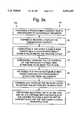
- FIG. 1is a cross sectional side view showing fabrication of a two-sided flexible high density multilayer interconnect structure prior to release from its carrier using methods in accordance with the principles of the present invention
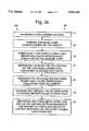
- FIGS. 2a, 2b and 2cshow fully fabricated two-sided flexible high density multilayer interconnect structures
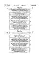
- FIGS. 3a-3iare flow diagrams illustrating details of various methods in accordance with the principles of the present invention.
- FIG. 1is a cross sectional side view showing fabrication of a two-sided flexible high density multilayer interconnect (HDMI) structure 10 or HDMI decal 10 fabricated Using methods 20 in accordance with the principles of the present invention.
- the present methods 20may be implemented using HDMI processes disclosed in U.S. Pat. No. 5,034,091 and U.S. Pat. No. 5,311,404, in addition to methods disclosed in the above-cited U.S. Patent Application entitled “HDMI Decal and Fine Line Flexible Interconnect Forming Methods", for example, all of which are assigned to the assignee of the present invention.
- the techniques disclosed in these referencesmay be adapted to produce the multilayer interconnect structure 10 on a rigid non-UV or non-laser absorbing carrier 11 as shown in FIG. 1.
- the flexible HDMI structure 10is fabricated on a relatively large carrier 11, typically having dimensions on the order of two feet by two feet.
- the carrier 11may comprise an ultraviolet transparent substrate 11 or wafer 11, such as quartz, for example, or may comprise a silicon wafer 11 or a metal carrier, for example, depending upon the release technique that is to be used to remove or release the flexible HDMI structures 10 from the carrier 11.
- the carrier 11has a release layer 12 formed or otherwise deposited thereon.
- a polyimide layer 12is deposited as the release layer 12.
- a metal or silicon dioxide layer 12is deposited as the release layer 12.
- the metal release layer 12may be comprised of titanium or tungsten, or mixtures thereof, for example.
- the two-sided flexible HDMI structure 10is comprised of a plurality of dielectric layers 15 having free line metallization patterns 13 and vias 14 formed therein that terminate at an upper set of contact pads 17 on the top surface of the structure 10.
- the free line metallization patterns 13include, but are not limited to, a bottom contact pad layer 13a, pad routing layers 13b, a ground layer 13c, an X-direction signal layer 13d, a Y-direction signal layer 13e, a power layer 13f and an upper contact pad layer 13g.
- the upper contact pad layer 13ghas a plurality of bond pads 17 coupled thereto that are used to connect to electronic components (not shown).
- each of the HDMI structures 10may comprise dielectric layers 15 comprising polyimide having aluminum or copper fine line interconnects 13 and vias 14 formed therethrough that provide signal paths from the upper set of bond pads 17 disposed at the surface of the two-sided HDMI structure 10 to the bottom contact pad layer 13a.
- the bottom contact pad layer 13ais connected to a lower set of bond pads 13a (FIGS. 2a and 2b) that are connected to electronic components (not shown).
- the plurality of two-sided HDMI structures 10are formed on the carrier 11 and release layer 12 using MCM-D (multichip module - dielectric) processing techniques employed by the assignee of the present invention. Processing that may be used to fabricate the two-sided HDMI structures 10 is described in U.S. Pat. No. 5,034,091, entitled "Method of Forming an Electrical Via Structure", and assigned to the assignee of the present invention, which is incorporated herein by reference in its entirety.
- FIGS. 2a and 2bshow fully fabricated two sided flexible high density multilayer interconnect structures (without electronic components) after it is released from the carrier 11.
- a short wavelength ultraviolet radiation source 19which is programmable and controlled, is used to release individual ones of the two-sided HDMI structures 10.
- a programmable pick and place machinemay be used to physically remove the two-sided HDMI structures 10 once they are released from the carrier 11.
- a flood beam ultraviolet radiation source 19may be used to release many or all of the two-sided HDMI structures 10 from the ultraviolet transparent substrate 11 or carrier 11.
- the ultraviolet radiation source 19is caused to radiate ultraviolet radiation through the ultraviolet transparent carrier 11 and onto the release layer 12.
- an ultraviolet lasermay be used to selectively irradiate one of the two-sided HDMI structures 10 to release it from the release layer 12.
- the ultraviolet radiation (photons) from the ultraviolet radiation source 19interacts with the polyimide release layer 12 adjacent to the carrier 11 and ruptures or otherwise breaks the adhesive bond therebetween. This permits the two-sided HDMI structures 10 to be lifted off of the carrier 11 using the programmable pick and place machine or other tool, for example. Multiple two-sided HDMI structures 10 may be released from the carrier 11 using a wide area ultraviolet radiation source 19 in a similar manner.
- the carrier 11comprises a silicon substrate 11
- a titanium or tungsten or mixture thereof metal layer 12, or a silicon dioxide layer 12is used as the release layer 12.
- An appropriate wet etching procedureis used to totally release the two-sided HDMI structures 10 from the release layer 12. Wet etching procedures are well known to those skilled in the art that will release the HDMI structures 10.
- the release layer 12 of the two-sided flexible HDMI structure 10must be processed to expose the bond pads at the bottom thereof. This may be achieved by temporarily bonding the top surface of the two-sided flexible HDMI structure 10 to an inert flat plate 32 using a temporary adhesive 31.
- the two-sided flexible HDMI structure 10is then released or delaminated from the carrier to expose bottom surface of the structure 10 (the polyimide release layer 12).
- Vias 16are formed through the polyimide release layer 12 to expose the bottom set of bond pads 13a. Additional metal is then deposited in the vias 16 and a bottom set of contact pads 18 are formed for the two-sided flexible HDMI structure 10 to which connections may be made.
- the second wayis to release the two-sided flexible HDMI structure 10 from the carrier 11. Then, the release layer 12 is removed to expose the bottom set of bond pads 13a.
- the exposed bottom set of bond pads 13amay be used as is to provide a bottom set of contact pads 18 for the flexible HDMI structure 10 to which connections may be made.
- This proceduremay also use the inert flat plate 32 that is temporarily bonded to the top surface of the two-sided flexible HDMI structure 10 during processing of the bottommost layers thereof. Because its use is optional, the inert flat plate 32 and adhesive 31 are shown in dashed lines in FIG. 2b.
- the third wayis to release the two-sided flexible HDMI structure 10 from the carrier 11. Then, the release layer 12 is removed to expose the bottom set of bond pads 13a. The exposed bottom set of bond pads 13a are then further processed to provide a bottom set of contact pads 18 for the flexible HDMI structure 10. This may be accomplished by depositing additional metal layers that contact the exposed bottom set of bond pads 13a, thusly forming the bottom set of contact pads 18 of the two-sided flexible HDMI structure 10 to which connections may be made. This procedure may also use the inert flat plate 32 that is temporarily bonded to the top surface of the two-sided flexible HDMI structure 10 during processing of the bottommost layers thereof. Because its use is optional, the inert flat plate 32 and adhesive 31 are shown in dashed lines in FIG. 2c.
- the two-sided flexible HDMI structure 10may be fully populated prior to exposing the bottom side thereof to a short wavelength high energy laser beam, or a short UV broad spectrum high intensity flash lamp that vaporizes the polyimide release layer 12 and exposes the set of bond pads adjacent the bottom side of the structure 10.
- FIGS. 3a-3ishow flow diagrams illustrating methods 20 in accordance with the present invention for forming two-sided flexible HDMI structures 10 on a carrier 11 and subsequently releasing them either individually or in total from the carrier 11.
- the present methods 20are as follows.
- a first method 20acomprises the steps of providing 21 a transparent carrier 11 that is transparent to ultraviolet radiation, and forming 22 a release layer 12 on the transparent carrier 11. Then two-sided flexible high density multilayer interconnect structures 10 are then fabricated 23 on the release layer 12. The top surface of the two-sided flexible HDMI structure 10 is then temporarily bonded 24 to an inert flat plate 32 using a temporary adhesive 31. The two-sided flexible HDMI structure 10 is then released 25 or delaminated 25 from the carrier 12 to expose the release layer 12. A laser is then used to form 26 vias 16 through the release layer 12 to expose the bottom set of bond pads 13a. A bottom set of contact pads 18 is formed for the two-sided flexible HDMI structure 10 by depositing 27 additional metal in the vias 16 and on the exposed bottom surface of the carrier 12.
- a second method 20bcomprises the steps of providing 21 a carrier 11, such as a silicon carrier 21a, forming 22 a release layer 12, such as a metal (titanium or tungsten or mixture thereof) release layer 12, on the carrier 11, fabricating 23 two-sided flexible high density multilayer interconnect structures 10 on the metal release layer 12.
- the top surface of the two-sided flexible HDMI structure 10is then temporarily bonded 24 to an inert flat plate 32 using a temporary adhesive 31.
- the two-sided flexible HDMI structure 10is then released 25 or delaminated 25 from the carrier to expose the release layer 12.
- a laseris then used to form 26 vias 16 through the release layer 12 to expose the bottom set of bond pads 13a.
- a bottom set of contact pads 18is formed 27 for the two-sided flexible HDMI structure 10 by depositing 27 additional metal in the vias 16 and on the exposed bottom surface of the carrier 12.
- a third method 20ccomprises the steps of providing 21 a carrier 11, such as a silicon carrier 11, forming 22 a release layer 12, such as a silicon dioxide release layer 12, on the rigid carrier 11, fabricating 23 two-sided flexible high density multilayer interconnect (HDMI) structures 10 on the release layer 12.
- the top surface of the two-sided flexible HDMI structure 10is then temporarily bonded 24 to an inert flat plate 32 using a temporary adhesive 31.
- the two-sided flexible HDMI structure 10is then released 25 or delaminated 25 from the carrier to expose the release layer 12.
- a laseris then used to form 26 vias 16 through the release layer 12 to expose the bottom set of bond pads 13a.
- a bottom set of contact pads 18is formed 27 for the two-sided flexible HDMI structure 10 by depositing 27 additional metal in the vias 16 and on the exposed bottom surface of the carrier 12.
- a fourth method 20dcomprises the steps of providing 21 a transparent carrier 11 that is transparent to ultraviolet radiation, and forming 22 a release layer 12 on the transparent carrier 11. Then two-sided flexible high density multilayer interconnect structures 10 are fabricated 23 on the release layer 12, and processed to release 25 the flexible HDMI structures 10 from the rigid carrier 11. The two-sided flexible high density multilayer interconnect structures 10 may be released 25 by irradiating the release layer 12 through the transparent carrier 11 using an ultraviolet radiation source 19. Then, the release layer 12 is removed 28 to expose the bottom set of bond pads 13a. The exposed bottom set of bond pads 13a are used as the bottom set of contact pads 18 of the flexible HDMI structure 10.
- a fifth method 20ecomprises the steps of providing 21 a carrier 11, such as a silicon carrier 11, forming 22 a release layer 12, such as a metal (titanium or tungsten or mixture thereof) release layer 12, on the carrier 11, fabricating 23 two-sided flexible high density multilayer interconnect structures 10 on the metal release layer 12, and processing the metal release layer 12 to release 25 the two-sided flexible HDMI structures 10 from the carrier 11, such as by using a wet etching procedure. Then, the release layer 12 is removed 28 to expose the bottom set of bond pads 13a. The exposed bottom set of bond pads 13a are used as the bottom set of contact pads 18 of the flexible HDMI structure 10.
- a sixth method 20fcomprises the steps of providing 21 a carrier 11, such as a silicon carrier 11, forming 22 a release layer 12, such as a silicon dioxide release layer 12, on the rigid carrier 11, fabricating 23 two-sided flexible high density multilayer interconnect (HDMI) structures 10 on the release layer 12, and processing the release layer 12 to release 25 the two-sided flexible HDMI structures 10 from the rigid carrier 11, such as by using a wet etching procedure. Then, the release layer 12 is removed 28 to expose the bottom set of bond pads 13a. The exposed bottom set of bond pads 13a are used as the bottom set of contact pads 18 of the flexible HDMI structure 10.
- a carrier 11such as a silicon carrier 11
- forming 22 a release layer 12such as a silicon dioxide release layer 12
- HDMIhigh density multilayer interconnect
- a seventh method 20gcomprises the steps of providing 21 a transparent carrier 11 that is transparent to ultraviolet radiation, and forming 22 a release layer 12 on the transparent carrier 11. Then two-sided flexible high density multilayer interconnect structures 10 are fabricated 23 on the release layer 12, and processed to release 25 the flexible HDMI structures 10 from the rigid carrier 11. The two-sided flexible high density multilayer interconnect structures 10 may be released 25 by irradiating the release layer 12 through the transparent carrier 11 using an ultraviolet radiation source 19. Then, the release layer 12 is removed 28 to expose the bottom set of bond pads 13a. The exposed bottom set of bond pads 13a are then further processed 29 to provide a bottom set of contact pads 18 for the flexible HDMI structure 10. This may be accomplished by depositing 29 additional metal layers that contact the exposed bottom set of bond pads 13a, thusly forming the bottom set of contact pads 18 of the two-sided flexible HDMI structure 10 to which connections may be made.
- an eighth method 20hcomprises the steps of providing 21 a carrier 11, such as a silicon carrier 11, forming 22 a release layer 12, such as a metal (titanium or tungsten or mixture thereof) release layer 12, on the carrier 11, fabricating 23 two-sided flexible high density multilayer interconnect structures 10 on the metal release layer 12, and processing the metal release layer 12 to release 25 the two-sided flexible HDMI structures 10 from the carrier 11, such as by using a wet etching procedure.
- the release layer 12is removed 28 to expose the bottom set of bond pads 13a.
- the exposed bottom set of bond pads 13aare then further processed 29 to provide a bottom set of contact pads 18 for the flexible HDMI structure 10. This may be accomplished by depositing 29 additional metal layers that contact the exposed bottom set of bond pads 13a, thusly forming the bottom set of contact pads 18 of the two-sided flexible HDMI structure 10 to which connections may be made.
- a ninth method 20icomprises the steps of providing 21 a carrier 11, such as a silicon carrier 11, forming 22 a release layer 12, such as a silicon dioxide release layer 12, on the rigid carrier 11, fabricating 23 two-sided flexible high density multilayer interconnect (HDMI) structures 10 on the release layer 12, and processing the release layer 12 to release 25 the two-sided flexible HDMI structures 10 from the rigid carrier 11, such as by using a wet etching procedure.
- the release layer 12is removed 28 to expose the bottom set of bond pads 13a.
- the exposed bottom set of bond pads 13aare then further processed 29 to provide a bottom set of contact pads 18 for the flexible HDMI structure 10. This may be accomplished by depositing 29 additional metal layers that contact the exposed bottom set of bond pads 13a, thusly forming the bottom set of contact pads 18 of the two-sided flexible HDMI structure 10 to which connections may be made.
Landscapes
- Engineering & Computer Science (AREA)
- Manufacturing & Machinery (AREA)
- Microelectronics & Electronic Packaging (AREA)
- Physics & Mathematics (AREA)
- Condensed Matter Physics & Semiconductors (AREA)
- General Physics & Mathematics (AREA)
- Computer Hardware Design (AREA)
- Power Engineering (AREA)
- Ceramic Engineering (AREA)
- Production Of Multi-Layered Print Wiring Board (AREA)
Abstract
Description
Claims (21)
Priority Applications (1)
| Application Number | Priority Date | Filing Date | Title |
|---|---|---|---|
| US08/738,558US5691245A (en) | 1996-10-28 | 1996-10-28 | Methods of forming two-sided HDMI interconnect structures |
Applications Claiming Priority (1)
| Application Number | Priority Date | Filing Date | Title |
|---|---|---|---|
| US08/738,558US5691245A (en) | 1996-10-28 | 1996-10-28 | Methods of forming two-sided HDMI interconnect structures |
Publications (1)
| Publication Number | Publication Date |
|---|---|
| US5691245Atrue US5691245A (en) | 1997-11-25 |
Family
ID=24968502
Family Applications (1)
| Application Number | Title | Priority Date | Filing Date |
|---|---|---|---|
| US08/738,558Expired - LifetimeUS5691245A (en) | 1996-10-28 | 1996-10-28 | Methods of forming two-sided HDMI interconnect structures |
Country Status (1)
| Country | Link |
|---|---|
| US (1) | US5691245A (en) |
Cited By (51)
| Publication number | Priority date | Publication date | Assignee | Title |
|---|---|---|---|---|
| US5817541A (en)* | 1997-03-20 | 1998-10-06 | Raytheon Company | Methods of fabricating an HDMI decal chip scale package |
| US5949246A (en)* | 1997-01-28 | 1999-09-07 | International Business Machines | Test head for applying signals in a burn-in test of an integrated circuit |
| US5998291A (en)* | 1997-04-07 | 1999-12-07 | Raytheon Company | Attachment method for assembly of high density multiple interconnect structures |
| US6365974B1 (en)* | 1999-03-23 | 2002-04-02 | Texas Instruments Incorporated | Flex circuit substrate for an integrated circuit package |
| US6408511B1 (en)* | 2000-08-21 | 2002-06-25 | National Semiconductor, Inc. | Method of creating an enhanced BGA attachment in a low-temperature co-fired ceramic (LTCC) substrate |
| US6524889B2 (en)* | 2000-08-23 | 2003-02-25 | Nec Corporation | Method of transcribing a wiring pattern from an original substrate to a substrate with closely matched thermal expansion coefficients between both substrates for dimensional control of the transcribed pattern |
| US20030199121A1 (en)* | 2000-07-27 | 2003-10-23 | Caletka David Vincent | Wafer scale thin film package |
| EP1376678A2 (en) | 2002-06-18 | 2004-01-02 | Sanyo Electric Co., Ltd. | Manufacturing method of semiconductor device |
| US20040203244A1 (en)* | 2002-02-13 | 2004-10-14 | Nobuo Oshima | Electronic component and fabricating method |
| US20040235270A1 (en)* | 2002-04-23 | 2004-11-25 | Sanyo Electric Co., Ltd. | Method of manufacturing semiconductor device |
| US20050176235A1 (en)* | 2002-06-18 | 2005-08-11 | Sanyo Electric Co., Ltd. | Manufacturing method of semiconductor device |
| US20060068576A1 (en)* | 2004-09-30 | 2006-03-30 | Burdick William E Jr | Lithography transfer for high density interconnect circuits |
| US20060100015A1 (en)* | 2004-10-01 | 2006-05-11 | Loose Timothy C | Digital audio in a wagering game system |
| US20070026639A1 (en)* | 2002-10-30 | 2007-02-01 | Sanyo Electric Co., Ltd. | Manufacturing method of semiconductor device |
| US7232740B1 (en) | 2005-05-16 | 2007-06-19 | The United States Of America As Represented By The National Security Agency | Method for bumping a thin wafer |
| US20070166957A1 (en)* | 2005-12-28 | 2007-07-19 | Sanyo Electric Co., Ltd | Method of manufacturing semiconductor device |
| US7297613B1 (en)* | 2005-06-09 | 2007-11-20 | The United States Of America As Represented By The National Security Agency | Method of fabricating and integrating high quality decoupling capacitors |
| US20080093708A1 (en)* | 2003-08-06 | 2008-04-24 | Sanyo Electric Co., Ltd. | Semiconductor device and manufacturing method thereof |
| US20080157235A1 (en)* | 2004-06-04 | 2008-07-03 | Rogers John A | Controlled buckling structures in semiconductor interconnects and nanomembranes for stretchable electronics |
| US7485562B2 (en)* | 2002-08-27 | 2009-02-03 | Micron Technology, Inc. | Method of making multichip wafer level packages and computing systems incorporating same |
| US7972875B2 (en) | 2007-01-17 | 2011-07-05 | The Board Of Trustees Of The University Of Illinois | Optical systems fabricated by printing-based assembly |
| US7982296B2 (en) | 2004-06-04 | 2011-07-19 | The Board Of Trustees Of The University Of Illinois | Methods and devices for fabricating and assembling printable semiconductor elements |
| US8008130B2 (en)* | 1999-10-05 | 2011-08-30 | Renesas Electronics Corporation | Multilayer interconnection board, semiconductor device having the same, and method of forming the same as well as method of mounting the semicondutor chip on the interconnection board |
| US8039847B2 (en) | 2004-06-04 | 2011-10-18 | The Board Of Trustees Of The University Of Illinois | Printable semiconductor structures and related methods of making and assembling |
| US20110318480A1 (en)* | 2008-12-17 | 2011-12-29 | Samsung Electro-Mechanics Co., Ltd. | Method of manufacturing substrate using a carrier |
| US8097926B2 (en) | 2008-10-07 | 2012-01-17 | Mc10, Inc. | Systems, methods, and devices having stretchable integrated circuitry for sensing and delivering therapy |
| US8198621B2 (en) | 2004-06-04 | 2012-06-12 | The Board Of Trustees Of The University Of Illinois | Stretchable form of single crystal silicon for high performance electronics on rubber substrates |
| US20130001791A1 (en)* | 2011-06-28 | 2013-01-03 | Broadcom Corporation | Method and Apparatuses for Integrated Circuit Substrate Manufacture |
| US8372726B2 (en) | 2008-10-07 | 2013-02-12 | Mc10, Inc. | Methods and applications of non-planar imaging arrays |
| US8389862B2 (en) | 2008-10-07 | 2013-03-05 | Mc10, Inc. | Extremely stretchable electronics |
| US8470701B2 (en) | 2008-04-03 | 2013-06-25 | Advanced Diamond Technologies, Inc. | Printable, flexible and stretchable diamond for thermal management |
| US20130203190A1 (en)* | 2012-02-02 | 2013-08-08 | Harris Corporation, Corporation Of The State Of Delaware | Method for making a redistributed wafer using transferrable redistribution layers |
| US8552299B2 (en) | 2008-03-05 | 2013-10-08 | The Board Of Trustees Of The University Of Illinois | Stretchable and foldable electronic devices |
| US8666471B2 (en) | 2010-03-17 | 2014-03-04 | The Board Of Trustees Of The University Of Illinois | Implantable biomedical devices on bioresorbable substrates |
| US8865489B2 (en) | 2009-05-12 | 2014-10-21 | The Board Of Trustees Of The University Of Illinois | Printed assemblies of ultrathin, microscale inorganic light emitting diodes for deformable and semitransparent displays |
| US8886334B2 (en) | 2008-10-07 | 2014-11-11 | Mc10, Inc. | Systems, methods, and devices using stretchable or flexible electronics for medical applications |
| US8934965B2 (en) | 2011-06-03 | 2015-01-13 | The Board Of Trustees Of The University Of Illinois | Conformable actively multiplexed high-density surface electrode array for brain interfacing |
| US9159635B2 (en) | 2011-05-27 | 2015-10-13 | Mc10, Inc. | Flexible electronic structure |
| US9171794B2 (en) | 2012-10-09 | 2015-10-27 | Mc10, Inc. | Embedding thin chips in polymer |
| US9289132B2 (en) | 2008-10-07 | 2016-03-22 | Mc10, Inc. | Catheter balloon having stretchable integrated circuitry and sensor array |
| US9442285B2 (en) | 2011-01-14 | 2016-09-13 | The Board Of Trustees Of The University Of Illinois | Optical component array having adjustable curvature |
| US9554484B2 (en) | 2012-03-30 | 2017-01-24 | The Board Of Trustees Of The University Of Illinois | Appendage mountable electronic devices conformable to surfaces |
| US9691873B2 (en) | 2011-12-01 | 2017-06-27 | The Board Of Trustees Of The University Of Illinois | Transient devices designed to undergo programmable transformations |
| US9723122B2 (en) | 2009-10-01 | 2017-08-01 | Mc10, Inc. | Protective cases with integrated electronics |
| US9765934B2 (en) | 2011-05-16 | 2017-09-19 | The Board Of Trustees Of The University Of Illinois | Thermally managed LED arrays assembled by printing |
| US9936574B2 (en) | 2009-12-16 | 2018-04-03 | The Board Of Trustees Of The University Of Illinois | Waterproof stretchable optoelectronics |
| US10441185B2 (en) | 2009-12-16 | 2019-10-15 | The Board Of Trustees Of The University Of Illinois | Flexible and stretchable electronic systems for epidermal electronics |
| US10918298B2 (en) | 2009-12-16 | 2021-02-16 | The Board Of Trustees Of The University Of Illinois | High-speed, high-resolution electrophysiology in-vivo using conformal electronics |
| US10925543B2 (en) | 2015-11-11 | 2021-02-23 | The Board Of Trustees Of The University Of Illinois | Bioresorbable silicon electronics for transient implants |
| US11029198B2 (en) | 2015-06-01 | 2021-06-08 | The Board Of Trustees Of The University Of Illinois | Alternative approach for UV sensing |
| US11118965B2 (en) | 2015-06-01 | 2021-09-14 | The Board Of Trustees Of The University Of Illinois | Miniaturized electronic systems with wireless power and near-field communication capabilities |
Citations (8)
| Publication number | Priority date | Publication date | Assignee | Title |
|---|---|---|---|---|
| US4980034A (en)* | 1989-04-04 | 1990-12-25 | Massachusetts Institute Of Technology | High-density, multi-level interconnects, flex circuits, and tape for TAB |
| US5039628A (en)* | 1988-02-19 | 1991-08-13 | Microelectronics & Computer Technology Corporation | Flip substrate for chip mount |
| US5192716A (en)* | 1989-01-25 | 1993-03-09 | Polylithics, Inc. | Method of making a extended integration semiconductor structure |
| US5196362A (en)* | 1990-08-28 | 1993-03-23 | Hitachi, Ltd. | Multilayer wiring method of on-chip modification for an lsi |
| US5262351A (en)* | 1990-08-21 | 1993-11-16 | Thomson-Csf | Process for manufacturing a multilayer integrated circuit interconnection |
| US5352926A (en)* | 1993-01-04 | 1994-10-04 | Motorola, Inc. | Flip chip package and method of making |
| US5400220A (en)* | 1994-05-18 | 1995-03-21 | Dell Usa, L.P. | Mechanical printed circuit board and ball grid array interconnect apparatus |
| US5514613A (en)* | 1994-01-27 | 1996-05-07 | Integrated Device Technology | Parallel manufacturing of semiconductor devices and the resulting structure |
- 1996
- 1996-10-28USUS08/738,558patent/US5691245A/ennot_activeExpired - Lifetime
Patent Citations (8)
| Publication number | Priority date | Publication date | Assignee | Title |
|---|---|---|---|---|
| US5039628A (en)* | 1988-02-19 | 1991-08-13 | Microelectronics & Computer Technology Corporation | Flip substrate for chip mount |
| US5192716A (en)* | 1989-01-25 | 1993-03-09 | Polylithics, Inc. | Method of making a extended integration semiconductor structure |
| US4980034A (en)* | 1989-04-04 | 1990-12-25 | Massachusetts Institute Of Technology | High-density, multi-level interconnects, flex circuits, and tape for TAB |
| US5262351A (en)* | 1990-08-21 | 1993-11-16 | Thomson-Csf | Process for manufacturing a multilayer integrated circuit interconnection |
| US5196362A (en)* | 1990-08-28 | 1993-03-23 | Hitachi, Ltd. | Multilayer wiring method of on-chip modification for an lsi |
| US5352926A (en)* | 1993-01-04 | 1994-10-04 | Motorola, Inc. | Flip chip package and method of making |
| US5514613A (en)* | 1994-01-27 | 1996-05-07 | Integrated Device Technology | Parallel manufacturing of semiconductor devices and the resulting structure |
| US5400220A (en)* | 1994-05-18 | 1995-03-21 | Dell Usa, L.P. | Mechanical printed circuit board and ball grid array interconnect apparatus |
Cited By (105)
| Publication number | Priority date | Publication date | Assignee | Title |
|---|---|---|---|---|
| US5949246A (en)* | 1997-01-28 | 1999-09-07 | International Business Machines | Test head for applying signals in a burn-in test of an integrated circuit |
| US5817541A (en)* | 1997-03-20 | 1998-10-06 | Raytheon Company | Methods of fabricating an HDMI decal chip scale package |
| US5998291A (en)* | 1997-04-07 | 1999-12-07 | Raytheon Company | Attachment method for assembly of high density multiple interconnect structures |
| US6365974B1 (en)* | 1999-03-23 | 2002-04-02 | Texas Instruments Incorporated | Flex circuit substrate for an integrated circuit package |
| US8008130B2 (en)* | 1999-10-05 | 2011-08-30 | Renesas Electronics Corporation | Multilayer interconnection board, semiconductor device having the same, and method of forming the same as well as method of mounting the semicondutor chip on the interconnection board |
| US20030199121A1 (en)* | 2000-07-27 | 2003-10-23 | Caletka David Vincent | Wafer scale thin film package |
| US20080119029A1 (en)* | 2000-07-27 | 2008-05-22 | David Vincent Caletka | Wafer scale thin film package |
| US7348261B2 (en)* | 2000-07-27 | 2008-03-25 | International Business Machines Corporation | Wafer scale thin film package |
| US6408511B1 (en)* | 2000-08-21 | 2002-06-25 | National Semiconductor, Inc. | Method of creating an enhanced BGA attachment in a low-temperature co-fired ceramic (LTCC) substrate |
| US6524889B2 (en)* | 2000-08-23 | 2003-02-25 | Nec Corporation | Method of transcribing a wiring pattern from an original substrate to a substrate with closely matched thermal expansion coefficients between both substrates for dimensional control of the transcribed pattern |
| US20040203244A1 (en)* | 2002-02-13 | 2004-10-14 | Nobuo Oshima | Electronic component and fabricating method |
| US20040235270A1 (en)* | 2002-04-23 | 2004-11-25 | Sanyo Electric Co., Ltd. | Method of manufacturing semiconductor device |
| US8105856B2 (en) | 2002-04-23 | 2012-01-31 | Semiconductor Components Industries, Llc | Method of manufacturing semiconductor device with wiring on side surface thereof |
| US20050176235A1 (en)* | 2002-06-18 | 2005-08-11 | Sanyo Electric Co., Ltd. | Manufacturing method of semiconductor device |
| EP2207198A3 (en)* | 2002-06-18 | 2011-06-29 | Sanyo Electric Co., Ltd. | Manufacturing method of a semiconductor device |
| EP1376678A3 (en)* | 2002-06-18 | 2004-02-04 | Sanyo Electric Co., Ltd. | Manufacturing method of semiconductor device |
| EP1376678A2 (en) | 2002-06-18 | 2004-01-02 | Sanyo Electric Co., Ltd. | Manufacturing method of semiconductor device |
| US7719102B2 (en) | 2002-06-18 | 2010-05-18 | Sanyo Electric Co., Ltd. | Semiconductor device |
| US7399683B2 (en) | 2002-06-18 | 2008-07-15 | Sanyo Electric Co., Ltd. | Manufacturing method of semiconductor device |
| US7485562B2 (en)* | 2002-08-27 | 2009-02-03 | Micron Technology, Inc. | Method of making multichip wafer level packages and computing systems incorporating same |
| US20070026639A1 (en)* | 2002-10-30 | 2007-02-01 | Sanyo Electric Co., Ltd. | Manufacturing method of semiconductor device |
| US7662670B2 (en) | 2002-10-30 | 2010-02-16 | Sanyo Electric Co., Ltd. | Manufacturing method of semiconductor device |
| US7919875B2 (en) | 2003-08-06 | 2011-04-05 | Sanyo Electric Co., Ltd. | Semiconductor device with recess portion over pad electrode |
| US20080093708A1 (en)* | 2003-08-06 | 2008-04-24 | Sanyo Electric Co., Ltd. | Semiconductor device and manufacturing method thereof |
| US8754396B2 (en) | 2004-06-04 | 2014-06-17 | The Board Of Trustees Of The University Of Illinois | Stretchable form of single crystal silicon for high performance electronics on rubber substrates |
| US9450043B2 (en) | 2004-06-04 | 2016-09-20 | The Board Of Trustees Of The University Of Illinois | Methods and devices for fabricating and assembling printable semiconductor elements |
| US9324733B2 (en) | 2004-06-04 | 2016-04-26 | The Board Of Trustees Of The University Of Illinois | Controlled buckling structures in semiconductor interconnects and nanomembranes for stretchable electronics |
| US9515025B2 (en) | 2004-06-04 | 2016-12-06 | The Board Of Trustees Of The University Of Illinois | Stretchable form of single crystal silicon for high performance electronics on rubber substrates |
| US9761444B2 (en) | 2004-06-04 | 2017-09-12 | The Board Of Trustees Of The University Of Illinois | Methods and devices for fabricating and assembling printable semiconductor elements |
| US9105555B2 (en) | 2004-06-04 | 2015-08-11 | The Board Of Trustees Of The University Of Illinois | Stretchable form of single crystal silicon for high performance electronics on rubber substrates |
| US7982296B2 (en) | 2004-06-04 | 2011-07-19 | The Board Of Trustees Of The University Of Illinois | Methods and devices for fabricating and assembling printable semiconductor elements |
| US9768086B2 (en) | 2004-06-04 | 2017-09-19 | The Board Of Trustees Of The University Of Illinois | Methods and devices for fabricating and assembling printable semiconductor elements |
| US8039847B2 (en) | 2004-06-04 | 2011-10-18 | The Board Of Trustees Of The University Of Illinois | Printable semiconductor structures and related methods of making and assembling |
| US10204864B2 (en) | 2004-06-04 | 2019-02-12 | The Board Of Trustees Of The University Of Illinois | Stretchable form of single crystal silicon for high performance electronics on rubber substrates |
| US12074213B2 (en) | 2004-06-04 | 2024-08-27 | The Board Of Trustees Of The University Of Illinois | Methods and devices for fabricating and assembling printable semiconductor elements |
| US8664699B2 (en) | 2004-06-04 | 2014-03-04 | The Board Of Trustees Of The University Of Illinois | Methods and devices for fabricating and assembling printable semiconductor elements |
| US8198621B2 (en) | 2004-06-04 | 2012-06-12 | The Board Of Trustees Of The University Of Illinois | Stretchable form of single crystal silicon for high performance electronics on rubber substrates |
| US8217381B2 (en) | 2004-06-04 | 2012-07-10 | The Board Of Trustees Of The University Of Illinois | Controlled buckling structures in semiconductor interconnects and nanomembranes for stretchable electronics |
| US11456258B2 (en) | 2004-06-04 | 2022-09-27 | The Board Of Trustees Of The University Of Illinois | Stretchable form of single crystal silicon for high performance electronics on rubber substrates |
| US10355113B2 (en) | 2004-06-04 | 2019-07-16 | The Board Of Trustees Of The University Of Illinois | Controlled buckling structures in semiconductor interconnects and nanomembranes for stretchable electronics |
| US11088268B2 (en) | 2004-06-04 | 2021-08-10 | The Board Of Trustees Of The University Of Illinois | Methods and devices for fabricating and assembling printable semiconductor elements |
| US8394706B2 (en) | 2004-06-04 | 2013-03-12 | The Board Of Trustees Of The University Of Illinois | Printable semiconductor structures and related methods of making and assembling |
| US8440546B2 (en) | 2004-06-04 | 2013-05-14 | The Board Of Trustees Of The University Of Illinois | Methods and devices for fabricating and assembling printable semiconductor elements |
| US20080157235A1 (en)* | 2004-06-04 | 2008-07-03 | Rogers John A | Controlled buckling structures in semiconductor interconnects and nanomembranes for stretchable electronics |
| US8729524B2 (en) | 2004-06-04 | 2014-05-20 | The Board Of Trustees Of The University Of Illinois | Controlled buckling structures in semiconductor interconnects and nanomembranes for stretchable electronics |
| US10374072B2 (en) | 2004-06-04 | 2019-08-06 | The Board Of Trustees Of The University Of Illinois | Methods and devices for fabricating and assembling printable semiconductor elements |
| US20060068576A1 (en)* | 2004-09-30 | 2006-03-30 | Burdick William E Jr | Lithography transfer for high density interconnect circuits |
| US20060100015A1 (en)* | 2004-10-01 | 2006-05-11 | Loose Timothy C | Digital audio in a wagering game system |
| US8517832B2 (en)* | 2004-10-01 | 2013-08-27 | Wms Gaming Inc. | Digital audio in a wagering game system |
| US7232740B1 (en) | 2005-05-16 | 2007-06-19 | The United States Of America As Represented By The National Security Agency | Method for bumping a thin wafer |
| US7297613B1 (en)* | 2005-06-09 | 2007-11-20 | The United States Of America As Represented By The National Security Agency | Method of fabricating and integrating high quality decoupling capacitors |
| US7795115B2 (en) | 2005-12-28 | 2010-09-14 | Sanyo Electric Co., Ltd. | Method of manufacturing semiconductor device |
| US20070166957A1 (en)* | 2005-12-28 | 2007-07-19 | Sanyo Electric Co., Ltd | Method of manufacturing semiconductor device |
| US10504882B2 (en) | 2007-01-17 | 2019-12-10 | The Board Of Trustees Of The University Of Illinois | Optical systems fabricated by printing-based assembly |
| US10424572B2 (en) | 2007-01-17 | 2019-09-24 | The Board Of Trustees Of The University Of Illinois | Optical systems fabricated by printing-based assembly |
| US11309305B2 (en) | 2007-01-17 | 2022-04-19 | The Board Of Trustees Of The University Of Illinois | Optical systems fabricated by printing-based assembly |
| US8722458B2 (en) | 2007-01-17 | 2014-05-13 | The Board Of Trustees Of The University Of Illinois | Optical systems fabricated by printing-based assembly |
| US12136620B2 (en) | 2007-01-17 | 2024-11-05 | The Board Of Trustees Of The University Of Illinois | Optical systems fabricated by printing-based assembly |
| US9601671B2 (en) | 2007-01-17 | 2017-03-21 | The Board Of Trustees Of The University Of Illinois | Optical systems fabricated by printing-based assembly |
| US10361180B2 (en) | 2007-01-17 | 2019-07-23 | The Board Of Trustees Of The University Of Illinois | Optical systems fabricated by printing-based assembly |
| US9117940B2 (en) | 2007-01-17 | 2015-08-25 | The Board Of Trustees Of The University Of Illinois | Optical systems fabricated by printing-based assembly |
| US7972875B2 (en) | 2007-01-17 | 2011-07-05 | The Board Of Trustees Of The University Of Illinois | Optical systems fabricated by printing-based assembly |
| US10064269B2 (en) | 2008-03-05 | 2018-08-28 | The Board Of Trustees Of The University Of Illinois | Stretchable and foldable electronic devices |
| US8905772B2 (en) | 2008-03-05 | 2014-12-09 | The Board Of Trustees Of The University Of Illinois | Stretchable and foldable electronic devices |
| US10292261B2 (en) | 2008-03-05 | 2019-05-14 | The Board Of Trustees Of The University Of Illinois | Stretchable and foldable electronic devices |
| US8552299B2 (en) | 2008-03-05 | 2013-10-08 | The Board Of Trustees Of The University Of Illinois | Stretchable and foldable electronic devices |
| US8470701B2 (en) | 2008-04-03 | 2013-06-25 | Advanced Diamond Technologies, Inc. | Printable, flexible and stretchable diamond for thermal management |
| US8536667B2 (en) | 2008-10-07 | 2013-09-17 | Mc10, Inc. | Systems, methods, and devices having stretchable integrated circuitry for sensing and delivering therapy |
| US9012784B2 (en) | 2008-10-07 | 2015-04-21 | Mc10, Inc. | Extremely stretchable electronics |
| US9516758B2 (en) | 2008-10-07 | 2016-12-06 | Mc10, Inc. | Extremely stretchable electronics |
| US9289132B2 (en) | 2008-10-07 | 2016-03-22 | Mc10, Inc. | Catheter balloon having stretchable integrated circuitry and sensor array |
| US8886334B2 (en) | 2008-10-07 | 2014-11-11 | Mc10, Inc. | Systems, methods, and devices using stretchable or flexible electronics for medical applications |
| US8097926B2 (en) | 2008-10-07 | 2012-01-17 | Mc10, Inc. | Systems, methods, and devices having stretchable integrated circuitry for sensing and delivering therapy |
| US8389862B2 (en) | 2008-10-07 | 2013-03-05 | Mc10, Inc. | Extremely stretchable electronics |
| US8372726B2 (en) | 2008-10-07 | 2013-02-12 | Mc10, Inc. | Methods and applications of non-planar imaging arrays |
| US20110318480A1 (en)* | 2008-12-17 | 2011-12-29 | Samsung Electro-Mechanics Co., Ltd. | Method of manufacturing substrate using a carrier |
| US8677618B2 (en)* | 2008-12-17 | 2014-03-25 | Samsung Electro-Mechanics Co., Ltd. | Method of manufacturing substrate using a carrier |
| US9647171B2 (en) | 2009-05-12 | 2017-05-09 | The Board Of Trustees Of The University Of Illinois | Printed assemblies of ultrathin, microscale inorganic light emitting diodes for deformable and semitransparent displays |
| US10546841B2 (en) | 2009-05-12 | 2020-01-28 | The Board Of Trustees Of The University Of Illinois | Printed assemblies of ultrathin, microscale inorganic light emitting diodes for deformable and semitransparent displays |
| US8865489B2 (en) | 2009-05-12 | 2014-10-21 | The Board Of Trustees Of The University Of Illinois | Printed assemblies of ultrathin, microscale inorganic light emitting diodes for deformable and semitransparent displays |
| US9723122B2 (en) | 2009-10-01 | 2017-08-01 | Mc10, Inc. | Protective cases with integrated electronics |
| US10918298B2 (en) | 2009-12-16 | 2021-02-16 | The Board Of Trustees Of The University Of Illinois | High-speed, high-resolution electrophysiology in-vivo using conformal electronics |
| US11057991B2 (en) | 2009-12-16 | 2021-07-06 | The Board Of Trustees Of The University Of Illinois | Waterproof stretchable optoelectronics |
| US10441185B2 (en) | 2009-12-16 | 2019-10-15 | The Board Of Trustees Of The University Of Illinois | Flexible and stretchable electronic systems for epidermal electronics |
| US9936574B2 (en) | 2009-12-16 | 2018-04-03 | The Board Of Trustees Of The University Of Illinois | Waterproof stretchable optoelectronics |
| US8666471B2 (en) | 2010-03-17 | 2014-03-04 | The Board Of Trustees Of The University Of Illinois | Implantable biomedical devices on bioresorbable substrates |
| US9986924B2 (en) | 2010-03-17 | 2018-06-05 | The Board Of Trustees Of The University Of Illinois | Implantable biomedical devices on bioresorbable substrates |
| US9442285B2 (en) | 2011-01-14 | 2016-09-13 | The Board Of Trustees Of The University Of Illinois | Optical component array having adjustable curvature |
| US9765934B2 (en) | 2011-05-16 | 2017-09-19 | The Board Of Trustees Of The University Of Illinois | Thermally managed LED arrays assembled by printing |
| US9159635B2 (en) | 2011-05-27 | 2015-10-13 | Mc10, Inc. | Flexible electronic structure |
| US10349860B2 (en) | 2011-06-03 | 2019-07-16 | The Board Of Trustees Of The University Of Illinois | Conformable actively multiplexed high-density surface electrode array for brain interfacing |
| US8934965B2 (en) | 2011-06-03 | 2015-01-13 | The Board Of Trustees Of The University Of Illinois | Conformable actively multiplexed high-density surface electrode array for brain interfacing |
| US8779598B2 (en)* | 2011-06-28 | 2014-07-15 | Broadcom Corporation | Method and apparatuses for integrated circuit substrate manufacture |
| US20130001791A1 (en)* | 2011-06-28 | 2013-01-03 | Broadcom Corporation | Method and Apparatuses for Integrated Circuit Substrate Manufacture |
| US10396173B2 (en) | 2011-12-01 | 2019-08-27 | The Board Of Trustees Of The University Of Illinois | Transient devices designed to undergo programmable transformations |
| US9691873B2 (en) | 2011-12-01 | 2017-06-27 | The Board Of Trustees Of The University Of Illinois | Transient devices designed to undergo programmable transformations |
| US8772058B2 (en)* | 2012-02-02 | 2014-07-08 | Harris Corporation | Method for making a redistributed wafer using transferrable redistribution layers |
| US20130203190A1 (en)* | 2012-02-02 | 2013-08-08 | Harris Corporation, Corporation Of The State Of Delaware | Method for making a redistributed wafer using transferrable redistribution layers |
| US10357201B2 (en) | 2012-03-30 | 2019-07-23 | The Board Of Trustees Of The University Of Illinois | Appendage mountable electronic devices conformable to surfaces |
| US10052066B2 (en) | 2012-03-30 | 2018-08-21 | The Board Of Trustees Of The University Of Illinois | Appendage mountable electronic devices conformable to surfaces |
| US9554484B2 (en) | 2012-03-30 | 2017-01-24 | The Board Of Trustees Of The University Of Illinois | Appendage mountable electronic devices conformable to surfaces |
| US9171794B2 (en) | 2012-10-09 | 2015-10-27 | Mc10, Inc. | Embedding thin chips in polymer |
| US11029198B2 (en) | 2015-06-01 | 2021-06-08 | The Board Of Trustees Of The University Of Illinois | Alternative approach for UV sensing |
| US11118965B2 (en) | 2015-06-01 | 2021-09-14 | The Board Of Trustees Of The University Of Illinois | Miniaturized electronic systems with wireless power and near-field communication capabilities |
| US10925543B2 (en) | 2015-11-11 | 2021-02-23 | The Board Of Trustees Of The University Of Illinois | Bioresorbable silicon electronics for transient implants |
Similar Documents
| Publication | Publication Date | Title |
|---|---|---|
| US5691245A (en) | Methods of forming two-sided HDMI interconnect structures | |
| US12148676B2 (en) | Embedded chip package and manufacturing method thereof | |
| US5998291A (en) | Attachment method for assembly of high density multiple interconnect structures | |
| US5774340A (en) | Planar redistribution structure and printed wiring device | |
| US5817541A (en) | Methods of fabricating an HDMI decal chip scale package | |
| US7408258B2 (en) | Interconnection circuit and electronic module utilizing same | |
| US8322030B1 (en) | Circuit-on-foil process for manufacturing a laminated semiconductor package substrate having embedded conductive patterns | |
| CN102479724B (en) | A method of manufacturing a heat dissipation gain type stacked semiconductor component | |
| US5480503A (en) | Process for producing circuitized layers and multilayer ceramic sub-laminates and composites thereof | |
| TWI221664B (en) | Structure of chip package and process thereof | |
| CN112164677A (en) | A kind of circuit pre-arrangement heat dissipation embedded package structure and manufacturing method thereof | |
| US6848176B2 (en) | Process for manufacturing flexible wiring boards | |
| JPH10214920A (en) | Improved type polytetrafluoroethylene thin film chip carrier | |
| JPS6149443A (en) | Method of producing chip interposer | |
| EP0284624A1 (en) | Method of forming a multichip integrated circuit package. | |
| US5724727A (en) | Method of forming electronic component | |
| TW201021102A (en) | Coreless substrate package with symmetric external dielectric layers | |
| JPH04345779A (en) | Manufacture of electric connecting element | |
| JP2002314257A (en) | Multilayer circuit board, manufacturing method thereof and electric assembly | |
| KR20010088866A (en) | Deposited thin build-up layer dimensions as a method of relieving stress in high density interconnect printed wiring board substrates | |
| CN112820713A (en) | Metal frame packaging substrate and manufacturing method thereof | |
| EP0801423B1 (en) | Hdmi decal and fine line flexible interconnect forming methods | |
| US6808643B2 (en) | Hybrid interconnect substrate and method of manufacture thereof | |
| KR101971402B1 (en) | Manufacturing method of pcb using transparent carrier | |
| JP7610563B2 (en) | Structure in which multiple components are embedded and packaged in layers and its manufacturing method |
Legal Events
| Date | Code | Title | Description |
|---|---|---|---|
| AS | Assignment | Owner name:HUGHES ELECTRONICS, CALIFORNIA Free format text:ASSIGNMENT OF ASSIGNORS INTEREST;ASSIGNORS:BAKHIT, GABRIEL G.;PILLAI, VINCENT A.;AVERKIOU, GEORGE;AND OTHERS;REEL/FRAME:008293/0091 Effective date:19961017 | |
| STCF | Information on status: patent grant | Free format text:PATENTED CASE | |
| FPAY | Fee payment | Year of fee payment:4 | |
| FEPP | Fee payment procedure | Free format text:PAYOR NUMBER ASSIGNED (ORIGINAL EVENT CODE: ASPN); ENTITY STATUS OF PATENT OWNER: LARGE ENTITY | |
| FPAY | Fee payment | Year of fee payment:8 | |
| FEPP | Fee payment procedure | Free format text:PAYER NUMBER DE-ASSIGNED (ORIGINAL EVENT CODE: RMPN); ENTITY STATUS OF PATENT OWNER: LARGE ENTITY Free format text:PAYOR NUMBER ASSIGNED (ORIGINAL EVENT CODE: ASPN); ENTITY STATUS OF PATENT OWNER: LARGE ENTITY | |
| FPAY | Fee payment | Year of fee payment:12 | |
| AS | Assignment | Owner name:RAYTHEON COMPANY, MASSACHUSETTS Free format text:MERGER;ASSIGNOR:HE HOLDINGS, INC.;REEL/FRAME:032038/0627 Effective date:19971217 |