US5686764A - Flip chip package with reduced number of package layers - Google Patents
Flip chip package with reduced number of package layersDownload PDFInfo
- Publication number
- US5686764A US5686764AUS08/619,909US61990996AUS5686764AUS 5686764 AUS5686764 AUS 5686764AUS 61990996 AUS61990996 AUS 61990996AUS 5686764 AUS5686764 AUS 5686764A
- Authority
- US
- United States
- Prior art keywords
- traces
- conductive layer
- substrate
- voltage supply
- signal
- Prior art date
- Legal status (The legal status is an assumption and is not a legal conclusion. Google has not performed a legal analysis and makes no representation as to the accuracy of the status listed.)
- Expired - Lifetime
Links
Images


Classifications
- H—ELECTRICITY
- H01—ELECTRIC ELEMENTS
- H01L—SEMICONDUCTOR DEVICES NOT COVERED BY CLASS H10
- H01L23/00—Details of semiconductor or other solid state devices
- H01L23/48—Arrangements for conducting electric current to or from the solid state body in operation, e.g. leads, terminal arrangements ; Selection of materials therefor
- H01L23/50—Arrangements for conducting electric current to or from the solid state body in operation, e.g. leads, terminal arrangements ; Selection of materials therefor for integrated circuit devices, e.g. power bus, number of leads
- H—ELECTRICITY
- H01—ELECTRIC ELEMENTS
- H01L—SEMICONDUCTOR DEVICES NOT COVERED BY CLASS H10
- H01L23/00—Details of semiconductor or other solid state devices
- H01L23/48—Arrangements for conducting electric current to or from the solid state body in operation, e.g. leads, terminal arrangements ; Selection of materials therefor
- H01L23/488—Arrangements for conducting electric current to or from the solid state body in operation, e.g. leads, terminal arrangements ; Selection of materials therefor consisting of soldered or bonded constructions
- H01L23/498—Leads, i.e. metallisations or lead-frames on insulating substrates, e.g. chip carriers
- H01L23/49838—Geometry or layout
- H—ELECTRICITY
- H01—ELECTRIC ELEMENTS
- H01L—SEMICONDUCTOR DEVICES NOT COVERED BY CLASS H10
- H01L23/00—Details of semiconductor or other solid state devices
- H01L23/552—Protection against radiation, e.g. light or electromagnetic waves
- H—ELECTRICITY
- H01—ELECTRIC ELEMENTS
- H01L—SEMICONDUCTOR DEVICES NOT COVERED BY CLASS H10
- H01L2924/00—Indexing scheme for arrangements or methods for connecting or disconnecting semiconductor or solid-state bodies as covered by H01L24/00
- H01L2924/0001—Technical content checked by a classifier
- H01L2924/0002—Not covered by any one of groups H01L24/00, H01L24/00 and H01L2224/00
- H—ELECTRICITY
- H01—ELECTRIC ELEMENTS
- H01L—SEMICONDUCTOR DEVICES NOT COVERED BY CLASS H10
- H01L2924/00—Indexing scheme for arrangements or methods for connecting or disconnecting semiconductor or solid-state bodies as covered by H01L24/00
- H01L2924/15—Details of package parts other than the semiconductor or other solid state devices to be connected
- H01L2924/151—Die mounting substrate
- H01L2924/1517—Multilayer substrate
- H01L2924/15172—Fan-out arrangement of the internal vias
- H01L2924/15173—Fan-out arrangement of the internal vias in a single layer of the multilayer substrate
- H—ELECTRICITY
- H01—ELECTRIC ELEMENTS
- H01L—SEMICONDUCTOR DEVICES NOT COVERED BY CLASS H10
- H01L2924/00—Indexing scheme for arrangements or methods for connecting or disconnecting semiconductor or solid-state bodies as covered by H01L24/00
- H01L2924/30—Technical effects
- H01L2924/301—Electrical effects
- H01L2924/3011—Impedance
Definitions
- the present inventionrelates to the field of electronic microcircuits. More particularly, the present intention relates to the field of reducing the complexity and number of layers within a "flip chip" microcircuit package.
- a “flip chip”refers to a microcircuit that includes at least one semiconductor die bonded circuit side down to a substrate, with direct electrical interconnection between the die and the substrate or package. Because the die is connected directly to the substrate, traditional bond wires are eliminated.
- the substratemay be a passive carrier such as a printed circuit board (PCB), or it may be another semiconductor chip. Flip chips of the latter type are described in U.S. Pat. No. 5,410,805.
- the substrateis normally bonded directly to a motherboard, on which may be mounted other flip chips and/or other chips employing a variety of more traditional packages such as leadframe packages, surface mount, pin grid arrays, and the like.
- the substrateserves is to allow the I/O signals on the die to "escape" the die onto the motherboard.
- Diesare usually quite small, and contain as many as hundreds of I/O signals, as well as numerous power and ground connections.
- the substrateserves the purpose of spreading out these densely packed bumps to a much less dense spacing, so that these I/O's along with power and ground can then be connected to the motherboard.
- a flip chipwhen the die is bonded to the substrate the bumps on the die are the points of physical and electrical contact between the die and the substrate.
- the bumpscarry electrical signals including power and ground to and from the die.
- a number of electrical characteristicsare desirable to be met: controlled impedance to minimize signal reflections, close coupling to the power and ground planes for good return current paths and resulting low inductance, low impedance particularly for power and ground connections, and wide spacing of signal traces to minimize crosstalk particularly when many signals may switch at the same time.
- flip chips having PCB substratestypically use at least four layers for the substrate: a first signal layer, a dedicated power plane, a second signal layer, and a dedicated ground plane. Ceramic substrates, because they have a higher dielectric constant than PCB material, may contain eight or more layers in order to achieve satisfactory performance when the die contains several hundred connections. Unfortunately, as the number of substrate layers rises so does the complexity and cost of the flip chip package.
- the number of layers necessary in a flip chip packageis reduced by providing a first substrate layer having small groups of I/O traces such as two traces per group, with each group of I/O traces having voltage supply traces such as power traces substantially parallel to and on either side of the two I/O traces.
- a second substrate layercontains similar groups of two traces, with each group of two traces having voltage supply traces such as ground traces on either side of the two I/O traces.
- the power and ground tracesmay be as wide as two I/O traces side by side.
- the I/O traces on the first substrate layerare aligned atop power traces on the second layer, and I/O traces on the second substrate layer are aligned below ground traces on the first substrate layer.
- the I/O signal groups on the first layerare shielded on both sides by power traces and are further shielded below by a ground trace, crosstalk between these I/O signals and other signals on the substrate is greatly reduced. Accordingly, the overall density of I/O traces may be increased. Additionally, separate power and ground layers are eliminated. The overall result is a reduction in the number of layers required for a flip chip substrate, with resulting lower manufacturing complexity and cost. For a flip chip of conventional construction having two I/O signal layers and dedicated power and ground planes, by eliminating the dedicated power and ground planes the construction of the present invention allows the number of substrate layers to be reduced from four to two.
- the present inventioncomprises a flip chip comprising an integrated circuit die and a substrate, the substrate having at least two conductive layers separated by an insulating dielectric layer, the two conductive layers each having a plurality of I/O signal traces and further having a plurality of voltage supply traces providing shielding for the I/O signal traces, the traces being substantially parallel and arranged in a repeating pattern of I/O signal traces followed by a voltage supply trace, the voltage supply traces on one conductive layer being arranged atop or below I/O signal traces on the other conductive layer.
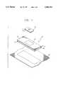
- FIG. 1is an exploded perspective drawing of a flip chip and a motherboard
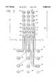
- FIG. 2is a bottom view of the die, showing the die pads or contacts and a top metallization layer.
- FIG. 3is a top view of a portion of a flip chip substrate according to a first embodiment of the present invention
- FIG. 4is a top view of a portion of a flip chip substrate according to a second embodiment of the present invention.
- FIG. 5is a top view of the substrate of FIG. 4, but with only the traces on the bottom surface of the substrate illustrated;
- FIG. 6is a top view of a portion of a flip chip substrate according to a third embodiment of the present invention.
- FIG. 7is a top view of the substrate of FIG. 6, but with only the traces on the bottom surface of the substrate illustrated;
- FIG. 8is a combined view of FIGS. 6 and 7.
- FIG. 1shows a flip chip and a motherboard 80.
- the flip chipincludes a die 10 and a substrate 30.
- Die 10is composed of a semiconductor material with an integrated circuit 12 formed on face side 11 of die 10.
- a passivation layer(not shown) such as a layer made of silicon nitride protects the face side 11 from scratching.
- Die 10is mounted face down, i.e., integrated circuit 12 down, to substrate 30.
- Die 10is bonded to substrate 30 at die bonding area 38. Bonding is typically by soldering.
- Substrate 30includes a first conductive layer 32, a dielectric layer 34 and a second conductive layer 36.
- Conductive layers 32 and 36are typically made of a copper base material plated onto dielectric layer 34, and typically patterned to create individual traces by a photolithographic process. Alternatively, substrate 30 could be formed of a plurality of layers fabricated separately and then laminated together.
- Dielectric layer 34is formed of an insulating dielectric material such as polyimide, PCB laminate, PTFE (TEFLONTM), FR4, BT resin, ceramic, or any other insulator used for semiconductor packages. Because the dielectric constant of ceramic is in the range of 9-10, while the dielectric constant of organic materials is in the range of 2.8-4.5, organic materials are usually preferred.
- substratesmay also be used, such as for example "decals" or printed double sided flex tape with or without stiffeners; although the illustrative embodiment focusses on a more traditional substrate, it will be understood that the present invention also applies to these newer types of substrates as well.
- FIG. 2illustrates the bump pattern on the face of die 10, including a top metallization layer, for the purpose of illustrating one example of a die to which the flip chip package of the present invention will apply.
- Die 10includes a plurality of I/O bumps 14, V DD (power) bumps 16, and V SS (ground) bumps 18 around the periphery.
- the bumps onare made of a high quality metal such as gold.
- V DD contacts 16supply power and V SS contacts 18 supply ground to I/O driver transistors within integrated circuit 12.
- a plurality of V DD2 (power) bumps 20 and V SS2 (ground) bumps 22supply power and ground to logic circuitry within integrated circuit 12.
- V DD2 contacts within a roware tied together by a wide trace comprising a bus bar.
- V SS2 contacts within a roware similarly tied together.
- V DD2 and V SS2may be kept separate from V DD and V SS , respectively, so that noise and transients on V SS and V DD due to switching of I/O drivers will not appear on the power and ground for the internal logic circuitry, which could cause logic errors.
- Spacing between contacts 14-22is typically on the order of 8-10 mils (203-254 microns).
- FIG. 2Although a substrate for a flip chip having a single square grid array of 20 ⁇ 20 bumps is shown in FIG. 2, other bump patterns are used, and the present invention is applicable to these other bump patterns as well. For purposes of the present discussion, the bumps will be assumed to be spaced at 250 micron intervals.
- first conductive layer 32is a plurality of contacts 40, 42, 44, 46, 48, and 50 for accommodating electrical connections between integrated circuit 12 and substrate 30.
- Die I/O contacts 40carry I/O signals from die area 38 across first conductive layer 32 to vias 60 which connect through to contact points called lands (not shown) on second conductive layer 36.
- a solder ballis typically connected to each land, for soldering to motherboard 80.
- the solder balls on second conductive layer 36are collectively termed the ball grid array, because they are usually arranged in a grid pattern.
- the spacing between ballsis typically 1.0 or 1.27 mm, though this spacing will undoubtedly decrease as the relevant technologies improve.
- the vias formed in substrate 30can be for example drilled vias, photo vias, or laser vias.
- V SS contacts 42carry V SS voltage supply from die area 38 over first conductive layer 32 to vias 62 which connect to solder balls on second conductive layer 36.
- V SS contacts 42carry V SS voltage supply from die area 38 over first conductive layer 32 to vias 62 which connect to solder balls on second conductive layer 36.
- the other half of the contacts around the periphery of die contact area 38comprise I/O contacts 44 and V DD contacts 46. These contacts connect immediately through vias to second conductive layer 36 and then radiate outwardly, in a manner similar to the traces on first conductive layer 32, to connect to the ball grid array.
- substrate 30serves the purpose of allowing electrical connections on die 10 spaced 250 microns apart to "escape" to electrical grid connections on motherboard 80, where the contacts are spaced 1.27 mm apart, or about five times as far apart. It will be noted that in this regard FIG. 3 is not drawn to scale.
- V SS2 contacts 48 and V DD2 contacts 50connect immediately through to second conductive layer 36 by vias.
- Wide tracessuch as those shown in FIG. 2 or partial planes may connect various V SS2 contacts together.
- wide traces or partial planesmay connect various V DD2 contacts together.
- the points of contact on motherboard 80 for V SS2 and V DD2may be partial planes.
- FIGS. 2 and 3are drawn illustrating a six row contact pattern, with a 4:1:1 ratio. This means that for every six contacts there are four I/O's plus one power and one ground. 0n each conductive layer there is a repeating pattern of two I/O traces followed by one voltage supply trace (either a power trace or a voltage trace).
- the 4:1:1 arrangementis particularly well suited for I/O signals that comprise differential pairs.
- I/O traces on first conductive layer 32are aligned above V DD traces on second conductive layer 36, and I/O traces on second conductive layer 36 are aligned below V SS traces on first conductive layer 32, so as to provide shielding either above or below for each I/O signal.
- the voltage supply tracesmay be at least as wide as approximately two I/O traces plus the width separating the traces. For example, in a 30/30 trace spacing, each I/O trace is 30 microns wide, and the two I/O traces are separated by a gap of 30 microns. In this trace spacing, each voltage supply trace is at least 90 microns wide.
- each group of I/O signalsis shielded on either side by a first voltage supply, and is further shielded either above or below by a second voltage supply. It is preferred that the voltage supply trace be slightly wider than the two I/O signal traces above or below it, so the actual width is chosen as 100 microns in the exemplary embodiment.
- This arrangementallows for a high degree of shielding between signals, thus reducing crosstalk between signal traces.
- the only two signal traces that will experience a higher degree of crosstalkare the two adjacent signal traces. If the two signal traces comprise a differential pair the crosstalk will generally not be a problem. If the signals are not a differential pair, or if other numbers of signals within a group such as three or four signals are used, the signals chosen for grouping can be such as to minimize the possibility of crosstalk induced errors.
- the repeating patternwould be one I/O trace followed by one voltage trace. This would reduce crosstalk every further.
- the repeating patternwould be three I/O traces followed by one voltage trace.
- the arrangement chosenwill depend on a number of factors, including the number of bumps available to service I/O transistors, the shielding required, etc. A number of factors that influence the required spacing and shielding between signals are well known. These factors include switching speeds, the number of signals switching at once, whether signals are synchronous or asynchronous, the relative timing between two or more synchronous signals, the dielectric constant of dielectric layer 34, and other considerations. In any of the arrangements discussed herein, the exact I/O and power/ground trace widths, and the spacing between traces, may be adjusted to provide the desired path impedances.
- V SS tracesare formed on first conductive layer 32
- V DD tracesare formed on second conductive layer 36.
- This configurationwas chosen with a die having V SS and V DD voltage supply rings around its periphery, with V SS on the outside and V DD on the inside, in mind.
- V DDthe inner voltage
- first conductive layer 32to carry V SS (the outer voltage) outward from die 10.
- the position of these voltage on the diecould be reversed, in which case it would be advantageous to reverse the voltages on conductive layers 32 and 36.
- FIG. 4illustrates a substrate in which V SS pad 70 connects through to the second conductive layer by via 72.
- V SS pad 70is covered by an insulating material, and V DD trace 74 routed atop V SS pad 72 using an additional metallization layer.
- the power and ground traceshave been shown in the figures for simplicity as wide, linear traces. However, in order to provide the greatest amount of noise and transient immunity, the power and ground traces should be spread out so as to cover as much of the first and second conductive layers as possible. When this is done the power and ground traces become closer to being power and ground planes, which provide better shielding and transient protection than linear traces. Additionally, it is desirable to connect V SS traces together and V DD traces together at various points, so that when a high switching load is experienced on one trace an adjacent trace can assist in sourcing or draining the switching current.
- FIGS. 4 and 5also illustrate a substrate layout in which a different number of I/O signals comprise respective groups on different sides of the substrate. Three I/O's are grouped together on the first conductive layer (FIG. 4), and a single I/O is shielded on the second conductive layer (FIG. 5).
- the repeating pattern on one substrate sidemay also be three I/O's followed by a power trace, one I/O followed by a ground trace, three I/O's followed by a power trace, one I/O followed by a ground trace, and so on. Generally speaking, the repeating pattern is at least one voltage supply trace followed by at least one I/O signal trace.
- FIGS. 6-8illustrate an embodiment in which the V SS and V DD contacts are not adjacent, but rather have an I/O contact interposed therebetween. These figures also illustrate that the voltage supply traces on the first conductive layer (FIG. 6) align atop I/O signals on the second conductive layer (FIG. 7), and vice versa. The combined traces are shown in FIG. 8.
- I/O driverscan be spaced at approximately 250 microns apart around the periphery of the die. This provides sufficient spacing for a wide voltage supply trace of 100 microns, followed by two 30/30 signals, i.e., a first space of 30 microns, a first I/O trace of 30 microns, a second space of 30 microns, a second I/O trace of 30 microns, and a third space of 30 microns. This pattern is then repeated. Thus, a power trace and two signal traces are provided, having an overall width of 250 microns at the periphery of the die. The pattern is repeated across the substrate. Because each I/O trace is adjacent and unshielded from only one other trace, each I/O signal receives substantial interference from only one other I/O signal.
- a three I/O patternmay be optimum in some applications, depending on the amount of tolerable crosstalk, the spacing between bumps, the desired trace impedance, cost, and other considerations.
- a 2:1:1 arrangement having a single I/O followed by a voltage traceis also possible. This would provide a very high degree of shielding, but would not provide as high an overall I/O trace density. This would be an attractive option, for example, for flip chips that operate at high speeds and with relatively few I/O signals.
- the teachings of the present inventioncan be applied to increasingly smaller packages and pinout patterns.
- the teachings of the present inventionare applicable to substrates having more than two layers. It is also possible to construct a substrate having only one conductive layer, with a repeating pattern of I/O traces followed by a voltage trace according to the present invention.
- flip chipsnormally have more I/O signals than can be suitably handled using only a single substrate layer.
- the present inventioncan be advantageously used to reduce the number of layers in a more complex substrate, as for example to reduce the number of layers necessary from six to four. Further, it will be noted that the approach of the present invention could be applied to improve the shielding between signals and/or reduce the number of layers necessary in a motherboard.
Landscapes
- Physics & Mathematics (AREA)
- Power Engineering (AREA)
- General Physics & Mathematics (AREA)
- Engineering & Computer Science (AREA)
- Computer Hardware Design (AREA)
- Microelectronics & Electronic Packaging (AREA)
- Condensed Matter Physics & Semiconductors (AREA)
- Geometry (AREA)
- Health & Medical Sciences (AREA)
- Electromagnetism (AREA)
- Toxicology (AREA)
- Wire Bonding (AREA)
- Structure Of Printed Boards (AREA)
Abstract
Description
Claims (18)
Priority Applications (2)
| Application Number | Priority Date | Filing Date | Title |
|---|---|---|---|
| US08/619,909US5686764A (en) | 1996-03-20 | 1996-03-20 | Flip chip package with reduced number of package layers |
| JP06817197AJP4592122B2 (en) | 1996-03-20 | 1997-03-21 | Flip chip package with reduced number of package layers |
Applications Claiming Priority (1)
| Application Number | Priority Date | Filing Date | Title |
|---|---|---|---|
| US08/619,909US5686764A (en) | 1996-03-20 | 1996-03-20 | Flip chip package with reduced number of package layers |
Publications (1)
| Publication Number | Publication Date |
|---|---|
| US5686764Atrue US5686764A (en) | 1997-11-11 |
Family
ID=24483823
Family Applications (1)
| Application Number | Title | Priority Date | Filing Date |
|---|---|---|---|
| US08/619,909Expired - LifetimeUS5686764A (en) | 1996-03-20 | 1996-03-20 | Flip chip package with reduced number of package layers |
Country Status (2)
| Country | Link |
|---|---|
| US (1) | US5686764A (en) |
| JP (1) | JP4592122B2 (en) |
Cited By (82)
| Publication number | Priority date | Publication date | Assignee | Title |
|---|---|---|---|---|
| US5838072A (en)* | 1997-02-24 | 1998-11-17 | Mosel Vitalic Corporation | Intrachip power distribution package and method for semiconductors having a supply node electrically interconnected with one or more intermediate nodes |
| US5885855A (en)* | 1996-11-12 | 1999-03-23 | Lsi Logic Corporation | Method for distributing connection pads on a semiconductor die |
| US6008532A (en)* | 1997-10-23 | 1999-12-28 | Lsi Logic Corporation | Integrated circuit package having bond fingers with alternate bonding areas |
| WO2000007242A1 (en)* | 1998-07-28 | 2000-02-10 | Infineon Technologies Ag | Conductor frame, printed circuit board with a conductor frame and a method for producing a conductor frame |
| US6043559A (en)* | 1996-09-09 | 2000-03-28 | Intel Corporation | Integrated circuit package which contains two in plane voltage busses and a wrap around conductive strip that connects a bond finger to one of the busses |
| US6150729A (en)* | 1999-07-01 | 2000-11-21 | Lsi Logic Corporation | Routing density enhancement for semiconductor BGA packages and printed wiring boards |
| US6225143B1 (en) | 1998-06-03 | 2001-05-01 | Lsi Logic Corporation | Flip-chip integrated circuit routing to I/O devices |
| US6246121B1 (en)* | 1999-04-12 | 2001-06-12 | Vlsi Technology, Inc. | High performance flip-chip semiconductor device |
| US6303423B1 (en) | 1998-12-21 | 2001-10-16 | Megic Corporation | Method for forming high performance system-on-chip using post passivation process |
| US6306751B1 (en) | 1999-09-27 | 2001-10-23 | Lsi Logic Corporation | Apparatus and method for improving ball joints in semiconductor packages |
| US6388890B1 (en)* | 2000-06-19 | 2002-05-14 | Nortel Networks Limited | Technique for reducing the number of layers in a multilayer circuit board |
| US6410990B2 (en)* | 1997-12-12 | 2002-06-25 | Intel Corporation | Integrated circuit device having C4 and wire bond connections |
| US6479758B1 (en)* | 2000-01-21 | 2002-11-12 | Kabushiki Kaisha Toshiba | Wiring board, semiconductor package and semiconductor device |
| US6489656B1 (en) | 2001-10-03 | 2002-12-03 | Megic Corporation | Resistor for high performance system-on-chip using post passivation process |
| US6495442B1 (en) | 2000-10-18 | 2002-12-17 | Magic Corporation | Post passivation interconnection schemes on top of the IC chips |
| US6507118B1 (en) | 2000-07-14 | 2003-01-14 | 3M Innovative Properties Company | Multi-metal layer circuit |
| US6518663B1 (en)* | 1999-08-30 | 2003-02-11 | Texas Instruments Incorporated | Constant impedance routing for high performance integrated circuit packaging |
| US6577004B1 (en)* | 2000-08-31 | 2003-06-10 | Micron Technology, Inc. | Solder ball landpad design to improve laminate performance |
| US6581189B1 (en)* | 1998-01-14 | 2003-06-17 | Advanced Micro Devices, Inc. | Computer implemented method and program for automating flip-chip bump layout in integrated circuit package design |
| US20030148604A1 (en)* | 2001-12-13 | 2003-08-07 | Mou-Shiung Lin | Chip structure and process for forming the same |
| US20030170934A1 (en)* | 1998-12-21 | 2003-09-11 | Megic Corporation | Top layers of metal for high performance IC's |
| US20030170977A1 (en)* | 2000-08-10 | 2003-09-11 | Weekly Roger D. | Routing for multilayer ceramic substrates to reduce excessive via depth |
| US6620728B2 (en) | 1998-12-21 | 2003-09-16 | Megic Corporation | Top layers of metal for high performance IC's |
| US20030179049A1 (en)* | 2002-02-05 | 2003-09-25 | Force10 Networks, Inc. | Passive transmission line equalization using circuit-board thru-holes |
| US6653691B2 (en) | 2000-11-16 | 2003-11-25 | Silicon Semiconductor Corporation | Radio frequency (RF) power devices having faraday shield layers therein |
| US6657293B1 (en)* | 1999-10-05 | 2003-12-02 | Nec Corporation | Chip scale package in which layout of wiring lines is improved |
| US20030222295A1 (en)* | 1998-12-21 | 2003-12-04 | Megic Corporation | High performance system-on-chip inductor using post passivation process |
| US6664620B2 (en)* | 1999-06-29 | 2003-12-16 | Intel Corporation | Integrated circuit die and/or package having a variable pitch contact array for maximization of number of signal lines per routing layer |
| US20030230428A1 (en)* | 2001-07-31 | 2003-12-18 | Liew Wee K. | PBGA electrical noise isolation of signal traces |
| US6674163B1 (en)* | 1998-08-18 | 2004-01-06 | Oki Electric Industry Co., Ltd. | Package structure for a semiconductor device |
| US20040016117A1 (en)* | 2000-06-19 | 2004-01-29 | Aneta Wyrzykowska | Technique for reducing the number of layers in a signal routing device |
| US20040016948A1 (en)* | 1998-12-21 | 2004-01-29 | Megic Corporation | High performance system-on-chip discrete components using post passivation process |
| US20040029404A1 (en)* | 1998-12-21 | 2004-02-12 | Megic Corporation | High performance system-on-chip passive device using post passivation process |
| WO2003058712A3 (en)* | 2002-01-07 | 2004-03-25 | Sun Microsystems Inc | Method for assigning power and ground pins in array packages to enhance next level routing |
| US20040099440A1 (en)* | 2000-06-19 | 2004-05-27 | Herman Kwong | Technique for accommodating electronic components on a multiplayer signal routing device |
| US20040136168A1 (en)* | 2000-06-19 | 2004-07-15 | Duxbury Guy M.A.F. | Techniques for reducing the number of layers in a multilayer signal routing device |
| US6768206B2 (en) | 2002-05-07 | 2004-07-27 | Kabushiki Kaisha Toshiba | Organic substrate for flip chip bonding |
| US20040166659A1 (en)* | 1998-12-21 | 2004-08-26 | Megic Corporation | Top layers of metal for high performance IC's |
| US6794750B2 (en)* | 1997-12-26 | 2004-09-21 | Nec Electronics Corporation | Semiconductor device |
| US20040212103A1 (en)* | 2000-06-19 | 2004-10-28 | Herman Kwong | Techniques for pin arrangements in circuit chips |
| US20040216071A1 (en)* | 2003-04-22 | 2004-10-28 | Miller Leah M. | Routing structure for transceiver core |
| US20040216916A1 (en)* | 2000-06-19 | 2004-11-04 | Aneta Wyrzykowska | Technique for improving power and ground flooding |
| US20040226742A1 (en)* | 2003-05-14 | 2004-11-18 | Aneta Wyrzykowska | Package modification for channel-routed circuit boards |
| US6833513B1 (en)* | 2002-10-22 | 2004-12-21 | Cisco Technology, Inc. | Crosstalk reduction in a PWB connector footprint |
| US20050110167A1 (en)* | 2003-11-24 | 2005-05-26 | Lsi Logic Corporation | Routing scheme for differential pairs in flip chip substrates |
| US20050139388A1 (en)* | 2003-02-10 | 2005-06-30 | Choi Jung-Hwan | Semiconductor devices having more than two-rows of pad structures and methods of fabricating the same |
| US20060049483A1 (en)* | 2004-09-09 | 2006-03-09 | Megic Corporation | Post passivation interconnection process and structures |
| US20060049524A1 (en)* | 2004-09-09 | 2006-03-09 | Megic Corporation | Post passivation interconnection process and structures |
| US20060049525A1 (en)* | 2004-09-09 | 2006-03-09 | Megic Corporation | Post passivation interconnection process and structures |
| US20060063371A1 (en)* | 2004-09-23 | 2006-03-23 | Megic Corporation | Top layers of metal for integrated circuits |
| US20060063378A1 (en)* | 2004-09-23 | 2006-03-23 | Megie Corporation | Top layers of metal for integrated circuits |
| US20060223341A1 (en)* | 2005-04-01 | 2006-10-05 | Arun Ramakrishnan | Ball assignment system |
| US20060248383A1 (en)* | 2005-04-28 | 2006-11-02 | Yukihiro Urakawa | Processing device on which processing elements having same function are embedded in one chip |
| US20070182521A1 (en)* | 2003-05-27 | 2007-08-09 | Megica Corporation | High performance system-on-chip inductor using post passivation process |
| US7281326B1 (en) | 2000-06-19 | 2007-10-16 | Nortel Network Limited | Technique for routing conductive traces between a plurality of electronic components of a multilayer signal routing device |
| US20080116581A1 (en)* | 2003-10-15 | 2008-05-22 | Megica Corporation | Post passivation interconnection schemes on top of the ic chips |
| US20080124918A1 (en)* | 1998-12-21 | 2008-05-29 | Megica Corporation | Chip structure and process for forming the same |
| US20080142979A1 (en)* | 2001-12-13 | 2008-06-19 | Megica Corporation | Chip structure and process for forming the same |
| US20080150094A1 (en)* | 2006-12-21 | 2008-06-26 | M/A-Com, Inc. | Flip chip shielded RF I/O land grid array package |
| US20080150623A1 (en)* | 2006-12-26 | 2008-06-26 | Megica Corporation | Voltage Regulator Integrated with Semiconductor Chip |
| US7409572B1 (en)* | 2003-12-05 | 2008-08-05 | Lsi Corporation | Low power memory controller with leaded double data rate DRAM package arranged on a two layer printed circuit board |
| US20080280463A1 (en)* | 2007-05-09 | 2008-11-13 | Mercury Computer Systems, Inc. | Rugged Chip Packaging |
| US20090001511A1 (en)* | 2005-03-29 | 2009-01-01 | Megica Corporation | High performance system-on-chip using post passivation process |
| US20090096082A1 (en)* | 2003-03-05 | 2009-04-16 | Banpil Photonics, Inc. | High speed electrical interconnects and method of manufacturing thereof |
| US20090170240A1 (en)* | 1998-02-19 | 2009-07-02 | Texas Instruments Incorporated | Optimized Circuit Design Layout for High Performance Ball Grid Array Packages |
| US20090193374A1 (en)* | 2008-01-10 | 2009-07-30 | Kazuhiko Fujimoto | Method of designing semiconductor integrated circuit device, designing apparatus, and semiconductor integrated circuit device |
| DE102008001204A1 (en)* | 2008-04-16 | 2009-10-22 | Robert Bosch Gmbh | Disposable filling |
| US7725860B1 (en) | 2000-06-19 | 2010-05-25 | Herman Kwong | Contact mapping using channel routing |
| US20100165585A1 (en)* | 2008-12-26 | 2010-07-01 | Megica Corporation | Chip packages with power management integrated circuits and related techniques |
| US7816610B2 (en) | 2007-04-19 | 2010-10-19 | Mediatek Inc. | Layout circuit |
| EP1310995A3 (en)* | 2001-11-13 | 2010-10-20 | Nxp B.V. | Device for shielding the signal lines by the ground or power lines |
| US7960269B2 (en) | 2005-07-22 | 2011-06-14 | Megica Corporation | Method for forming a double embossing structure |
| US7973629B2 (en) | 2001-09-04 | 2011-07-05 | Megica Corporation | Method for making high-performance RF integrated circuits |
| US20120068362A1 (en)* | 2000-06-08 | 2012-03-22 | Renesas Electronics Corporation | Semiconductor device having semiconductor member and mounting member |
| US20120098125A1 (en)* | 2010-10-21 | 2012-04-26 | Via Technologies, Inc. | Integrated circuit package and physical layer interface arrangement |
| US20120126398A1 (en)* | 2010-11-23 | 2012-05-24 | Via Technologies, Inc. | Integrated circuit package and physical layer interface arrangement |
| US8421158B2 (en) | 1998-12-21 | 2013-04-16 | Megica Corporation | Chip structure with a passive device and method for forming the same |
| US20150189750A1 (en)* | 2014-01-02 | 2015-07-02 | Byoung Wook Jang | Package substrates and integrated circuit packages including the same |
| US20150228602A1 (en)* | 2014-02-12 | 2015-08-13 | Sony Corporation | Semicondcutor chip and semionducot module |
| CN111261605A (en)* | 2018-12-03 | 2020-06-09 | 爱思开海力士有限公司 | semiconductor package |
| CN111276458A (en)* | 2018-12-04 | 2020-06-12 | 爱思开海力士有限公司 | semiconductor package |
| US20210343764A1 (en)* | 2018-10-25 | 2021-11-04 | Sony Semiconductor Solutions Corporation | Circuit board, semiconductor apparatus, and electronic equipment |
Citations (9)
| Publication number | Priority date | Publication date | Assignee | Title |
|---|---|---|---|---|
| JPH05144879A (en)* | 1991-11-25 | 1993-06-11 | Fujitsu General Ltd | Chip parts mounting structure |
| US5237448A (en)* | 1991-02-05 | 1993-08-17 | American Ingenuity, Inc. | Visibility enhancing material |
| US5258648A (en)* | 1991-06-27 | 1993-11-02 | Motorola, Inc. | Composite flip chip semiconductor device with an interposer having test contacts formed along its periphery |
| US5281151A (en)* | 1991-07-05 | 1994-01-25 | Hitachi, Ltd. | Semiconductor chip carrier, module having same chip carrier mounted therein, and electronic device incorporating same module |
| WO1994024704A1 (en)* | 1993-04-12 | 1994-10-27 | Bolger Justin C | Area bonding conductive adhesive preforms |
| US5381307A (en)* | 1992-06-19 | 1995-01-10 | Motorola, Inc. | Self-aligning electrical contact array |
| US5391917A (en)* | 1993-05-10 | 1995-02-21 | International Business Machines Corporation | Multiprocessor module packaging |
| US5510758A (en)* | 1993-04-07 | 1996-04-23 | Matsushita Electric Industrial Co., Ltd. | Multilayer microstrip wiring board with a semiconductor device mounted thereon via bumps |
| US5523622A (en)* | 1992-11-24 | 1996-06-04 | Hitachi, Ltd. | Semiconductor integrated device having parallel signal lines |
- 1996
- 1996-03-20USUS08/619,909patent/US5686764A/ennot_activeExpired - Lifetime
- 1997
- 1997-03-21JPJP06817197Apatent/JP4592122B2/ennot_activeExpired - Lifetime
Patent Citations (9)
| Publication number | Priority date | Publication date | Assignee | Title |
|---|---|---|---|---|
| US5237448A (en)* | 1991-02-05 | 1993-08-17 | American Ingenuity, Inc. | Visibility enhancing material |
| US5258648A (en)* | 1991-06-27 | 1993-11-02 | Motorola, Inc. | Composite flip chip semiconductor device with an interposer having test contacts formed along its periphery |
| US5281151A (en)* | 1991-07-05 | 1994-01-25 | Hitachi, Ltd. | Semiconductor chip carrier, module having same chip carrier mounted therein, and electronic device incorporating same module |
| JPH05144879A (en)* | 1991-11-25 | 1993-06-11 | Fujitsu General Ltd | Chip parts mounting structure |
| US5381307A (en)* | 1992-06-19 | 1995-01-10 | Motorola, Inc. | Self-aligning electrical contact array |
| US5523622A (en)* | 1992-11-24 | 1996-06-04 | Hitachi, Ltd. | Semiconductor integrated device having parallel signal lines |
| US5510758A (en)* | 1993-04-07 | 1996-04-23 | Matsushita Electric Industrial Co., Ltd. | Multilayer microstrip wiring board with a semiconductor device mounted thereon via bumps |
| WO1994024704A1 (en)* | 1993-04-12 | 1994-10-27 | Bolger Justin C | Area bonding conductive adhesive preforms |
| US5391917A (en)* | 1993-05-10 | 1995-02-21 | International Business Machines Corporation | Multiprocessor module packaging |
Non-Patent Citations (12)
| Title |
|---|
| A Design Methodology for the Interconnected Mesh Power System (IMPS) MCM Technology, 1995 IEPS Conference, pp. 192 196 no month.* |
| A Design Methodology for the Interconnected Mesh Power System (IMPS) MCM Technology, 1995 IEPS Conference, pp. 192-196 no month. |
| A Low Cost Multichip Module Using Flex Substrate and Ball Grid Array, ICEMCM 96 Proceedings, pp. 28 32 no month.* |
| A Low Cost Multichip Module Using Flex Substrate and Ball Grid Array, ICEMCM '96 Proceedings, pp. 28-32 no month. |
| A Signal Noise Comparison of the Interconnected Mesh Power System (IMPS) with a Standard Four Layer MCM Topology, 1996, Michael D. Glover et al. no month.* |
| A Signal-Noise Comparison of the Interconnected Mesh Power System (IMPS) with a Standard Four-Layer MCM Topology, 1996, Michael D. Glover et al. no month. |
| Design of the Interconnected Mesh Power System (IMPS) MCM Topology, MCM 94 Proceedings, pp. 543 548 no month.* |
| Design of the Interconnected Mesh Power System (IMPS) MCM Topology, MCM '94 Proceedings, pp. 543-548 no month. |
| Electrical Characterization of the Interconnected Mesh Power System (IMPS) MCM Topology, IEEE Transactions On Components, Packaging, and Manufacturing Technology Part B, vol. 18, No. 1, Feb. 1995, pp.99 105.* |
| Electrical Characterization of the Interconnected Mesh Power System (IMPS) MCM Topology, IEEE Transactions On Components, Packaging, and Manufacturing Technology-Part B, vol. 18, No. 1, Feb. 1995, pp.99-105. |
| Theory and Experimental Confirmation of the Interconnected Mesh Power System (IMPS) MCM Topology, The International Journal of Microcircuits and Electronic Packaging, vol. 18, No. 2, Second Quarter 1995 (ISSN 1063 1674), pp. 146 153 no month.* |
| Theory and Experimental Confirmation of the Interconnected Mesh Power System (IMPS) MCM Topology, The International Journal of Microcircuits and Electronic Packaging, vol. 18, No. 2, Second Quarter 1995 (ISSN 1063-1674), pp. 146-153 no month. |
Cited By (292)
| Publication number | Priority date | Publication date | Assignee | Title |
|---|---|---|---|---|
| US6043559A (en)* | 1996-09-09 | 2000-03-28 | Intel Corporation | Integrated circuit package which contains two in plane voltage busses and a wrap around conductive strip that connects a bond finger to one of the busses |
| US6440770B1 (en) | 1996-09-09 | 2002-08-27 | Intel Corporation | Integrated circuit package |
| US5885855A (en)* | 1996-11-12 | 1999-03-23 | Lsi Logic Corporation | Method for distributing connection pads on a semiconductor die |
| US5952726A (en)* | 1996-11-12 | 1999-09-14 | Lsi Logic Corporation | Flip chip bump distribution on die |
| US5838072A (en)* | 1997-02-24 | 1998-11-17 | Mosel Vitalic Corporation | Intrachip power distribution package and method for semiconductors having a supply node electrically interconnected with one or more intermediate nodes |
| US6008532A (en)* | 1997-10-23 | 1999-12-28 | Lsi Logic Corporation | Integrated circuit package having bond fingers with alternate bonding areas |
| US6727597B2 (en) | 1997-12-12 | 2004-04-27 | Intel Corporation | Integrated circuit device having C4 and wire bond connections |
| US6410990B2 (en)* | 1997-12-12 | 2002-06-25 | Intel Corporation | Integrated circuit device having C4 and wire bond connections |
| US6794750B2 (en)* | 1997-12-26 | 2004-09-21 | Nec Electronics Corporation | Semiconductor device |
| US6581189B1 (en)* | 1998-01-14 | 2003-06-17 | Advanced Micro Devices, Inc. | Computer implemented method and program for automating flip-chip bump layout in integrated circuit package design |
| US20090170240A1 (en)* | 1998-02-19 | 2009-07-02 | Texas Instruments Incorporated | Optimized Circuit Design Layout for High Performance Ball Grid Array Packages |
| US8039320B2 (en)* | 1998-02-19 | 2011-10-18 | Texas Instruments Incorporated | Optimized circuit design layout for high performance ball grid array packages |
| US6225143B1 (en) | 1998-06-03 | 2001-05-01 | Lsi Logic Corporation | Flip-chip integrated circuit routing to I/O devices |
| US6674166B2 (en) | 1998-06-03 | 2004-01-06 | Lsi Logic Corporation | Flip-chip integrated circuit routing to I/O devices |
| US6798045B2 (en) | 1998-07-28 | 2004-09-28 | Infineon Technologies Ag | Lead frame, circuit board with lead frame, and method for producing the lead frame |
| WO2000007242A1 (en)* | 1998-07-28 | 2000-02-10 | Infineon Technologies Ag | Conductor frame, printed circuit board with a conductor frame and a method for producing a conductor frame |
| US6674163B1 (en)* | 1998-08-18 | 2004-01-06 | Oki Electric Industry Co., Ltd. | Package structure for a semiconductor device |
| US20080044976A1 (en)* | 1998-12-21 | 2008-02-21 | Megica Corporation | High performance system-on-chip using post passivation process |
| US20080038869A1 (en)* | 1998-12-21 | 2008-02-14 | Megica Corporation | High performance system-on-chip using post passivation process |
| US7368376B2 (en) | 1998-12-21 | 2008-05-06 | Mou-Shiung Lin | Top layers of metal for high performance IC's |
| US7358610B2 (en) | 1998-12-21 | 2008-04-15 | Mou-Shiung Lin | Top layers of metal for high performance IC's |
| US7442969B2 (en) | 1998-12-21 | 2008-10-28 | Mou-Shiung Lin | Top layers of metal for high performance IC's |
| US7372155B2 (en) | 1998-12-21 | 2008-05-13 | Mou-Shiung Lin | Top layers of metal for high performance IC's |
| US20030071326A1 (en)* | 1998-12-21 | 2003-04-17 | Megic Corporation | High performance system-on-chip using post passivation process |
| US20080124918A1 (en)* | 1998-12-21 | 2008-05-29 | Megica Corporation | Chip structure and process for forming the same |
| US6489647B1 (en) | 1998-12-21 | 2002-12-03 | Megic Corporation | Capacitor for high performance system-on-chip using post passivation process structure |
| US8531038B2 (en) | 1998-12-21 | 2013-09-10 | Megica Corporation | Top layers of metal for high performance IC's |
| US8487400B2 (en) | 1998-12-21 | 2013-07-16 | Megica Corporation | High performance system-on-chip using post passivation process |
| US20030170934A1 (en)* | 1998-12-21 | 2003-09-11 | Megic Corporation | Top layers of metal for high performance IC's |
| US7382058B2 (en) | 1998-12-21 | 2008-06-03 | Mou-Shiung Lin | Top layers of metal for high performance IC's |
| US6620728B2 (en) | 1998-12-21 | 2003-09-16 | Megic Corporation | Top layers of metal for high performance IC's |
| US8471384B2 (en) | 1998-12-21 | 2013-06-25 | Megica Corporation | Top layers of metal for high performance IC's |
| US20080083987A1 (en)* | 1998-12-21 | 2008-04-10 | Mou-Shiung Lin | Top layers of metal for high performance IC's |
| US7385292B2 (en) | 1998-12-21 | 2008-06-10 | Mou-Shiung Lin | Top layers of metal for high performance IC's |
| US8421158B2 (en) | 1998-12-21 | 2013-04-16 | Megica Corporation | Chip structure with a passive device and method for forming the same |
| US6657310B2 (en) | 1998-12-21 | 2003-12-02 | Magic Corporation | Top layers of metal for high performance IC's |
| US7384864B2 (en) | 1998-12-21 | 2008-06-10 | Mou-Shiung Lin | Top layers of metal for high performance IC's |
| US20030222295A1 (en)* | 1998-12-21 | 2003-12-04 | Megic Corporation | High performance system-on-chip inductor using post passivation process |
| US20070290355A1 (en)* | 1998-12-21 | 2007-12-20 | Mou-Shiung Lin | Top layers of metal for high performance IC's |
| US8415800B2 (en) | 1998-12-21 | 2013-04-09 | Megica Corporation | Top layers of metal for high performance IC's |
| US8368204B2 (en) | 1998-12-21 | 2013-02-05 | Megica Corporation | Chip structure and process for forming the same |
| US20080048329A1 (en)* | 1998-12-21 | 2008-02-28 | Mou-Shiung Lin | Top layers of metal for high performance IC's |
| US20080050913A1 (en)* | 1998-12-21 | 2008-02-28 | Mou-Shiung Lin | Top layers of metal for high performance IC's |
| US20040016948A1 (en)* | 1998-12-21 | 2004-01-29 | Megic Corporation | High performance system-on-chip discrete components using post passivation process |
| US20040029404A1 (en)* | 1998-12-21 | 2004-02-12 | Megic Corporation | High performance system-on-chip passive device using post passivation process |
| US20040041211A1 (en)* | 1998-12-21 | 2004-03-04 | Megic Corporation | Post passivation interconnection schemes on top of the IC chips |
| US8350386B2 (en) | 1998-12-21 | 2013-01-08 | Megica Corporation | Top layers of metal for high performance IC's |
| US6455885B1 (en) | 1998-12-21 | 2002-09-24 | Megic Corporation | Inductor structure for high performance system-on-chip using post passivation process |
| US8304907B2 (en) | 1998-12-21 | 2012-11-06 | Megica Corporation | Top layers of metal for integrated circuits |
| US7385291B2 (en) | 1998-12-21 | 2008-06-10 | Mou-Shiung Lin | Top layers of metal for high performance IC's |
| US7388292B2 (en) | 1998-12-21 | 2008-06-17 | Mou-Shiung Lin | Top layers of metal for high performance IC's |
| US8178435B2 (en) | 1998-12-21 | 2012-05-15 | Megica Corporation | High performance system-on-chip inductor using post passivation process |
| US20040166659A1 (en)* | 1998-12-21 | 2004-08-26 | Megic Corporation | Top layers of metal for high performance IC's |
| US6303423B1 (en) | 1998-12-21 | 2001-10-16 | Megic Corporation | Method for forming high performance system-on-chip using post passivation process |
| US7372085B2 (en) | 1998-12-21 | 2008-05-13 | Mou-Shiung Lin | Top layers of metal for high performance IC's |
| US20080146020A1 (en)* | 1998-12-21 | 2008-06-19 | Mou-Shiung Lin | Top layers of metal for high performance IC's |
| US20080042273A1 (en)* | 1998-12-21 | 2008-02-21 | Megica Corporation | High performance system-on-chip using post passivation process |
| US8129265B2 (en) | 1998-12-21 | 2012-03-06 | Megica Corporation | High performance system-on-chip discrete components using post passivation process |
| US20080142980A1 (en)* | 1998-12-21 | 2008-06-19 | Mou-Shiung Lin | Top layers of metal for high performance IC's |
| US8089155B2 (en) | 1998-12-21 | 2012-01-03 | Megica Corporation | High performance system-on-chip discrete components using post passivation process |
| US20070290357A1 (en)* | 1998-12-21 | 2007-12-20 | Mou-Shiung Lin | Top layers of metal for high performance IC's |
| US8035227B2 (en) | 1998-12-21 | 2011-10-11 | Megica Corporation | Top layers of metal for high performance IC's |
| US6869870B2 (en) | 1998-12-21 | 2005-03-22 | Megic Corporation | High performance system-on-chip discrete components using post passivation process |
| US7396756B2 (en) | 1998-12-21 | 2008-07-08 | Mou-Shiung Lin | Top layers of metal for high performance IC's |
| US6897507B2 (en) | 1998-12-21 | 2005-05-24 | Megic Corporation | Capacitor for high performance system-on-chip using post passivation device |
| US8022545B2 (en) | 1998-12-21 | 2011-09-20 | Megica Corporation | Top layers of metal for high performance IC's |
| US8022546B2 (en) | 1998-12-21 | 2011-09-20 | Megica Corporation | Top layers of metal for high performance IC's |
| US20080035972A1 (en)* | 1998-12-21 | 2008-02-14 | Megica Corporation | High performance system-on-chip using post passivation process |
| US20050184358A1 (en)* | 1998-12-21 | 2005-08-25 | Megic Corporation | High performance system-on-chip using post passivation process |
| US7999384B2 (en) | 1998-12-21 | 2011-08-16 | Megica Corporation | Top layers of metal for high performance IC's |
| US20050200023A1 (en)* | 1998-12-21 | 2005-09-15 | Mou-Shiung Lin | Top layers of metal for high performance IC's |
| US20050208757A1 (en)* | 1998-12-21 | 2005-09-22 | Mou-Shiung Lin | Top layers of metal for high performance IC's |
| US20050245067A1 (en)* | 1998-12-21 | 2005-11-03 | Mou-Shiung Lin | Top layers of metal for high performance IC's |
| US6965165B2 (en) | 1998-12-21 | 2005-11-15 | Mou-Shiung Lin | Top layers of metal for high performance IC's |
| US7443033B2 (en) | 1998-12-21 | 2008-10-28 | Megica Corporation | Post passivation interconnection schemes on top of the IC chips |
| US20050260849A1 (en)* | 1998-12-21 | 2005-11-24 | Mou-Shiung Lin | Top layers of metal for high performance IC's |
| US20050266612A1 (en)* | 1998-12-21 | 2005-12-01 | Mou-Shiung Lin | Top layers of metal for high performance IC's |
| US20060012049A1 (en)* | 1998-12-21 | 2006-01-19 | Mou-Shiung Lin | Top layers of metal for high performance IC's |
| US20060038231A9 (en)* | 1998-12-21 | 2006-02-23 | Megic Corporation | Post passivation interconnection schemes on top of the IC chips |
| US20060043594A1 (en)* | 1998-12-21 | 2006-03-02 | Mou-Shiung Lin | Top layers of metal for high performance IC's |
| US7915157B2 (en) | 1998-12-21 | 2011-03-29 | Megica Corporation | Chip structure and process for forming the same |
| US7906422B2 (en) | 1998-12-21 | 2011-03-15 | Megica Corporation | Chip structure and process for forming the same |
| US7906849B2 (en) | 1998-12-21 | 2011-03-15 | Megica Corporation | Chip structure and process for forming the same |
| US20060051955A1 (en)* | 1998-12-21 | 2006-03-09 | Mou-Shiung Lin | Top layers of metal for high performance IC's |
| US7884479B2 (en) | 1998-12-21 | 2011-02-08 | Megica Corporation | Top layers of metal for high performance IC's |
| US7863654B2 (en) | 1998-12-21 | 2011-01-04 | Megica Corporation | Top layers of metal for high performance IC's |
| US20070290354A1 (en)* | 1998-12-21 | 2007-12-20 | Mou-Shiung Lin | Top layers of metal for high performance IC's |
| US7329954B2 (en) | 1998-12-21 | 2008-02-12 | Mou-Shiung Lin | Top layers of metal for high performance IC's |
| US20090309225A1 (en)* | 1998-12-21 | 2009-12-17 | Megica Corporation | Top layers of metal for high performance IC's |
| US7397135B2 (en) | 1998-12-21 | 2008-07-08 | Mou-Shiung Lin | Top layers of metal for high performance IC's |
| US7405149B1 (en) | 1998-12-21 | 2008-07-29 | Megica Corporation | Post passivation method for semiconductor chip or wafer |
| US20070290353A1 (en)* | 1998-12-21 | 2007-12-20 | Mou-Shiung Lin | Top layers of metal for high performance IC's |
| US7420276B2 (en) | 1998-12-21 | 2008-09-02 | Megica Corporation | Post passivation structure for semiconductor chip or wafer |
| US20090146307A1 (en)* | 1998-12-21 | 2009-06-11 | Megica Corporation | Top layers of metal for high performance IC's |
| US7531417B2 (en) | 1998-12-21 | 2009-05-12 | Megica Corporation | High performance system-on-chip passive device using post passivation process |
| US7422976B2 (en) | 1998-12-21 | 2008-09-09 | Mou-Shiung Lin | Top layers of metal for high performance IC's |
| US7482693B2 (en) | 1998-12-21 | 2009-01-27 | Mou-Shiung Lin | Top layers of metal for high performance IC's |
| US20070181970A1 (en)* | 1998-12-21 | 2007-08-09 | Megica Corporation | High performance system-on-chip inductor using post passivation process |
| US7422941B2 (en) | 1998-12-21 | 2008-09-09 | Megica Corporation | High performance system-on-chip using post passivation process |
| US7465975B2 (en) | 1998-12-21 | 2008-12-16 | Mou-Shiung Lin | Top layers of metal for high performance IC's |
| US7459761B2 (en) | 1998-12-21 | 2008-12-02 | Megica Corporation | High performance system-on-chip using post passivation process |
| US7456100B2 (en) | 1998-12-21 | 2008-11-25 | Mou-Shiung Lin | Top layers of metal for high performance IC's |
| US7425764B2 (en) | 1998-12-21 | 2008-09-16 | Mou-Shiung Lin | Top layers of metal for high performance IC's |
| US7294871B2 (en) | 1998-12-21 | 2007-11-13 | Mou-Shiung Lin | Top layers of metal for high performance IC's |
| US7294870B2 (en) | 1998-12-21 | 2007-11-13 | Mou-Shiung Lin | Top layers of metal for high performance IC's |
| US20070262455A1 (en)* | 1998-12-21 | 2007-11-15 | Mou-Shiung Lin | Top layers of metal for high performance IC's |
| US20070262458A1 (en)* | 1998-12-21 | 2007-11-15 | Mou-Shiung Lin | Top layers of metal for high performance IC's |
| US20070273038A1 (en)* | 1998-12-21 | 2007-11-29 | Mou-Shiung Lin | Top layers of metal for high performance IC's |
| US20070273041A1 (en)* | 1998-12-21 | 2007-11-29 | Mou-Shiung Lin | Top layers of metal for high performance IC's |
| US20070273039A1 (en)* | 1998-12-21 | 2007-11-29 | Mou-Shiung Lin | Top layers of metal for high performance IC's |
| US20070273037A1 (en)* | 1998-12-21 | 2007-11-29 | Mou-Shiung Lin | Top layers of metal for high performance IC's |
| US20070273040A1 (en)* | 1998-12-21 | 2007-11-29 | Mou-Shiung Lin | Top layers of metal for high performance IC's |
| US20070273034A1 (en)* | 1998-12-21 | 2007-11-29 | Mou-Shiung Lin | Top layers of metal for high performance IC's |
| US20070273036A1 (en)* | 1998-12-21 | 2007-11-29 | Mou-Shiung Lin | Top layers of metal for high performance IC's |
| US20070278691A1 (en)* | 1998-12-21 | 2007-12-06 | Mou-Shiung Lin | Top layers of metal for high performance IC's |
| US20070278679A1 (en)* | 1998-12-21 | 2007-12-06 | Mou-Shiung Lin | Top layers of metal for high performance IC's |
| US20070278685A1 (en)* | 1998-12-21 | 2007-12-06 | Mou-Shiung Lin | Top layers of metal for high performance IC's |
| US20070278690A1 (en)* | 1998-12-21 | 2007-12-06 | Mou-Shiung Lin | Top layers of metal for high performance IC's |
| US20070278684A1 (en)* | 1998-12-21 | 2007-12-06 | Mou-Shiung Lin | Top layers of metal for high performance IC's |
| US20070281463A1 (en)* | 1998-12-21 | 2007-12-06 | Mou-Shiung Lin | Top layers of metal for high performance IC's |
| US20070281467A1 (en)* | 1998-12-21 | 2007-12-06 | Mou-Shiung Lin | Top layers of metal for high performance IC's |
| US20070281468A1 (en)* | 1998-12-21 | 2007-12-06 | Mou-Shiung Lin | Top layers of metal for high performance IC's |
| US20070278687A1 (en)* | 1998-12-21 | 2007-12-06 | Mou-Shiung Lin | Top layers of metal for high performance IC's |
| US20070278689A1 (en)* | 1998-12-21 | 2007-12-06 | Mou-Shiung Lin | Top layers of metal for high performance IC's |
| US20070284739A1 (en)* | 1998-12-21 | 2007-12-13 | Mou-Shiung Lin | Top layers of metal for high performance IC's |
| US20070293036A1 (en)* | 1998-12-21 | 2007-12-20 | Mou-Shiung Lin | Top layers of metal for high performance IC's |
| US20070293037A1 (en)* | 1998-12-21 | 2007-12-20 | Mou-Shiung Lin | Top layers of metal for high performance IC's |
| US20070290352A1 (en)* | 1998-12-21 | 2007-12-20 | Mou-Shiung Lin | Top layers of metal for high performance IC's |
| US6246121B1 (en)* | 1999-04-12 | 2001-06-12 | Vlsi Technology, Inc. | High performance flip-chip semiconductor device |
| US7030479B2 (en) | 1999-06-29 | 2006-04-18 | Intel Corporation | Integrated circuit die and/or package having a variable pitch contact array for maximization of number of signal lines per routing layer |
| US6664620B2 (en)* | 1999-06-29 | 2003-12-16 | Intel Corporation | Integrated circuit die and/or package having a variable pitch contact array for maximization of number of signal lines per routing layer |
| US6150729A (en)* | 1999-07-01 | 2000-11-21 | Lsi Logic Corporation | Routing density enhancement for semiconductor BGA packages and printed wiring boards |
| US6518663B1 (en)* | 1999-08-30 | 2003-02-11 | Texas Instruments Incorporated | Constant impedance routing for high performance integrated circuit packaging |
| US6306751B1 (en) | 1999-09-27 | 2001-10-23 | Lsi Logic Corporation | Apparatus and method for improving ball joints in semiconductor packages |
| US6657293B1 (en)* | 1999-10-05 | 2003-12-02 | Nec Corporation | Chip scale package in which layout of wiring lines is improved |
| US6479758B1 (en)* | 2000-01-21 | 2002-11-12 | Kabushiki Kaisha Toshiba | Wiring board, semiconductor package and semiconductor device |
| US20120068362A1 (en)* | 2000-06-08 | 2012-03-22 | Renesas Electronics Corporation | Semiconductor device having semiconductor member and mounting member |
| US8680691B2 (en)* | 2000-06-08 | 2014-03-25 | Renesas Electronics Corporation | Semiconductor device having semiconductor member and mounting member |
| US7725860B1 (en) | 2000-06-19 | 2010-05-25 | Herman Kwong | Contact mapping using channel routing |
| US20040099440A1 (en)* | 2000-06-19 | 2004-05-27 | Herman Kwong | Technique for accommodating electronic components on a multiplayer signal routing device |
| US7281326B1 (en) | 2000-06-19 | 2007-10-16 | Nortel Network Limited | Technique for routing conductive traces between a plurality of electronic components of a multilayer signal routing device |
| US7259336B2 (en)* | 2000-06-19 | 2007-08-21 | Nortel Networks Limited | Technique for improving power and ground flooding |
| US6545876B1 (en)* | 2000-06-19 | 2003-04-08 | Nortel Networks Limited | Technique for reducing the number of layers in a multilayer circuit board |
| US20060254810A1 (en)* | 2000-06-19 | 2006-11-16 | Nortel Networks Limited | Technique for accommodating electronic components on a multilayer signal routing device |
| US20040216916A1 (en)* | 2000-06-19 | 2004-11-04 | Aneta Wyrzykowska | Technique for improving power and ground flooding |
| US7069646B2 (en) | 2000-06-19 | 2006-07-04 | Nortel Networks Limited | Techniques for reducing the number of layers in a multilayer signal routing device |
| US20040212103A1 (en)* | 2000-06-19 | 2004-10-28 | Herman Kwong | Techniques for pin arrangements in circuit chips |
| US6388890B1 (en)* | 2000-06-19 | 2002-05-14 | Nortel Networks Limited | Technique for reducing the number of layers in a multilayer circuit board |
| US20040136168A1 (en)* | 2000-06-19 | 2004-07-15 | Duxbury Guy M.A.F. | Techniques for reducing the number of layers in a multilayer signal routing device |
| US7069650B2 (en)* | 2000-06-19 | 2006-07-04 | Nortel Networks Limited | Method for reducing the number of layers in a multilayer signal routing device |
| US20040016117A1 (en)* | 2000-06-19 | 2004-01-29 | Aneta Wyrzykowska | Technique for reducing the number of layers in a signal routing device |
| US7107673B2 (en) | 2000-06-19 | 2006-09-19 | Nortel Networks Limited | Technique for accommodating electronic components on a multiplayer signal routing device |
| US6507118B1 (en) | 2000-07-14 | 2003-01-14 | 3M Innovative Properties Company | Multi-metal layer circuit |
| US6885098B2 (en)* | 2000-08-10 | 2005-04-26 | International Business Machines Corporation | Routing for multilayer ceramic substrates to reduce excessive via depth |
| US20030170977A1 (en)* | 2000-08-10 | 2003-09-11 | Weekly Roger D. | Routing for multilayer ceramic substrates to reduce excessive via depth |
| US20030205807A1 (en)* | 2000-08-31 | 2003-11-06 | Rumsey Brad D. | Solder ball landpad design to improve laminate performance |
| US20030193089A1 (en)* | 2000-08-31 | 2003-10-16 | Rumsey Brad D. | Solder ball landpad design to improve laminate performance |
| US6577004B1 (en)* | 2000-08-31 | 2003-06-10 | Micron Technology, Inc. | Solder ball landpad design to improve laminate performance |
| US6914326B2 (en) | 2000-08-31 | 2005-07-05 | Micron Technology, Inc. | Solder ball landpad design to improve laminate performance |
| US7951646B2 (en) | 2000-08-31 | 2011-05-31 | Round Rock Research, Llc | Solder ball landpad design to improve laminate performance |
| US20080045001A1 (en)* | 2000-10-18 | 2008-02-21 | Megica Corporation | Post passivation interconnection schemes on top of IC chip |
| US8004088B2 (en) | 2000-10-18 | 2011-08-23 | Megica Corporation | Post passivation interconnection schemes on top of IC chip |
| US8492900B2 (en) | 2000-10-18 | 2013-07-23 | Megica Corporation | Post passivation interconnection schemes on top of IC chip |
| US20080085596A1 (en)* | 2000-10-18 | 2008-04-10 | Megica Corporation | Post passivation interconnection schemes on top of IC chips |
| US6605528B1 (en) | 2000-10-18 | 2003-08-12 | Megic Corporation | Post passivation metal scheme for high-performance integrated circuit devices |
| US7382052B2 (en) | 2000-10-18 | 2008-06-03 | Mou-Shiung Lin | Post passivation interconnection schemes on top of IC chip |
| US20080067693A1 (en)* | 2000-10-18 | 2008-03-20 | Megica Corporation | Post passivation interconnection schemes on top of IC chip |
| US8482127B2 (en) | 2000-10-18 | 2013-07-09 | Megica Corporation | Post passivation interconnection schemes on top of IC chip |
| US6495442B1 (en) | 2000-10-18 | 2002-12-17 | Magic Corporation | Post passivation interconnection schemes on top of the IC chips |
| US20080057703A1 (en)* | 2000-10-18 | 2008-03-06 | Megica Corporation | Post passivation interconnection schemes on top of IC chip |
| US20080042293A1 (en)* | 2000-10-18 | 2008-02-21 | Megica Corporation | Post passivation interconnection schemes on top of IC chip |
| US20080045008A1 (en)* | 2000-10-18 | 2008-02-21 | Megica Corporation | Post passivation interconnection schemes on top of IC chip |
| US8461686B2 (en) | 2000-10-18 | 2013-06-11 | Megica Corporation | Post passivation interconnection schemes on top of IC chip |
| US20080045004A1 (en)* | 2000-10-18 | 2008-02-21 | Megica Corporation | Post passivation interconnection schemes on top of IC chips |
| US8435883B2 (en) | 2000-10-18 | 2013-05-07 | Megica Corporation | Post passivation interconnection schemes on top of IC chips |
| US7466007B2 (en) | 2000-10-18 | 2008-12-16 | Megica Corporation | Post passivation interconnection schemes on top of IC chip |
| US6734563B2 (en) | 2000-10-18 | 2004-05-11 | Megic Corporation | Post passivation interconnection schemes on top of the IC chips |
| US20080042295A1 (en)* | 2000-10-18 | 2008-02-21 | Megica Corporation | Post passivation interconnection schemes on top of IC chip |
| USRE43674E1 (en) | 2000-10-18 | 2012-09-18 | Megica Corporation | Post passivation metal scheme for high-performance integrated circuit devices |
| US8188603B2 (en) | 2000-10-18 | 2012-05-29 | Megica Corporation | Post passivation interconnection schemes on top of IC chip |
| US20080009131A1 (en)* | 2000-10-18 | 2008-01-10 | Megica Corporation | Post passivation interconnection schemes on top of the ic chips |
| US7479450B2 (en) | 2000-10-18 | 2009-01-20 | Megica Corporation | Post passivation interconnection schemes on top of the IC chips |
| US7923366B2 (en) | 2000-10-18 | 2011-04-12 | Megica Corporation | Post passivation interconnection schemes on top of IC chip |
| US20080006946A1 (en)* | 2000-10-18 | 2008-01-10 | Megica Corporation | Post passivation interconnection schemes on top of the ic chips |
| US20080001293A1 (en)* | 2000-10-18 | 2008-01-03 | Megica Corporation | Post passivation interconnection schemes on top of IC chip |
| US20080001302A1 (en)* | 2000-10-18 | 2008-01-03 | Megica Corporation | Post passivation interconnection schemes on top of IC chip |
| US7919865B2 (en) | 2000-10-18 | 2011-04-05 | Megica Corporation | Post passivation interconnection schemes on top of IC chip |
| US20080003806A1 (en)* | 2000-10-18 | 2008-01-03 | Megica Corporation | Post passivation interconnection schemes on top of IC chip |
| US7915161B2 (en) | 2000-10-18 | 2011-03-29 | Megica Corporation | Post passivation interconnection schemes on top of IC chip |
| US7439627B2 (en) | 2000-10-18 | 2008-10-21 | Megica Corporation | Post passivation interconnection schemes on top of the IC chips |
| US7439626B2 (en) | 2000-10-18 | 2008-10-21 | Megica Corporation | Post passivation interconnection schemes on top of IC chip |
| US20080001301A1 (en)* | 2000-10-18 | 2008-01-03 | Megica Corporation | Post passivation interconnection schemes on top of IC chip |
| US20080001294A1 (en)* | 2000-10-18 | 2008-01-03 | Megica Corporation | Post passivation interconnection schemes on top of IC chip |
| US7446031B2 (en) | 2000-10-18 | 2008-11-04 | Megica Corporation | Post passivation interconnection schemes on top of IC chips |
| US7446035B2 (en) | 2000-10-18 | 2008-11-04 | Megica Corporation | Post passivation interconnection schemes on top of IC chips |
| US7902067B2 (en) | 2000-10-18 | 2011-03-08 | Megica Corporation | Post passivation interconnection schemes on top of the IC chips |
| US20080085597A1 (en)* | 2000-10-18 | 2008-04-10 | Megica Corporation | Post passivation interconnection schemes on top of IC chips |
| US7892965B2 (en) | 2000-10-18 | 2011-02-22 | Megica Corporation | Post passivation interconnection schemes on top of IC chip |
| US7459791B2 (en) | 2000-10-18 | 2008-12-02 | Megica Corporation | Post passivation interconnection schemes on top of IC chip |
| US7534718B2 (en) | 2000-10-18 | 2009-05-19 | Megica Corporation | Post passivation interconnection schemes on top of IC chips |
| US7462938B2 (en) | 2000-10-18 | 2008-12-09 | Megica Corporation | Post passivation interconnection schemes on top of IC chip |
| US7524759B2 (en) | 2000-10-18 | 2009-04-28 | Megica Corporation | Post passivation interconnection schemes on top of IC chip |
| US6653691B2 (en) | 2000-11-16 | 2003-11-25 | Silicon Semiconductor Corporation | Radio frequency (RF) power devices having faraday shield layers therein |
| EP2287889A2 (en) | 2000-11-27 | 2011-02-23 | Megica Corporation | High performance system-on-chip using post passivation process |
| EP2287891A2 (en) | 2000-11-27 | 2011-02-23 | Megica Corporation | High performance system-on-chip using post passivation process |
| EP2287890A2 (en) | 2000-11-27 | 2011-02-23 | Megica Corporation | High performance system-on-chip using post passivation process |
| US6825554B2 (en)* | 2001-07-31 | 2004-11-30 | Lsi Logic Corporation | PBGA electrical noise isolation of signal traces |
| US20030230428A1 (en)* | 2001-07-31 | 2003-12-18 | Liew Wee K. | PBGA electrical noise isolation of signal traces |
| US7973629B2 (en) | 2001-09-04 | 2011-07-05 | Megica Corporation | Method for making high-performance RF integrated circuits |
| US8384508B2 (en) | 2001-09-04 | 2013-02-26 | Megica Corporation | Method for making high-performance RF integrated circuits |
| US6515369B1 (en)* | 2001-10-03 | 2003-02-04 | Megic Corporation | High performance system-on-chip using post passivation process |
| US6489656B1 (en) | 2001-10-03 | 2002-12-03 | Megic Corporation | Resistor for high performance system-on-chip using post passivation process |
| EP1310995A3 (en)* | 2001-11-13 | 2010-10-20 | Nxp B.V. | Device for shielding the signal lines by the ground or power lines |
| US8008776B2 (en) | 2001-12-13 | 2011-08-30 | Megica Corporation | Chip structure and process for forming the same |
| US8211791B2 (en) | 2001-12-13 | 2012-07-03 | Megica Corporation | Method for fabricating circuitry component |
| US8546947B2 (en)* | 2001-12-13 | 2013-10-01 | Megica Corporation | Chip structure and process for forming the same |
| US20030148604A1 (en)* | 2001-12-13 | 2003-08-07 | Mou-Shiung Lin | Chip structure and process for forming the same |
| US20110278727A1 (en)* | 2001-12-13 | 2011-11-17 | Megica Corporation | Chip structure and process for forming the same |
| US7919867B2 (en) | 2001-12-13 | 2011-04-05 | Megica Corporation | Chip structure and process for forming the same |
| US7932603B2 (en) | 2001-12-13 | 2011-04-26 | Megica Corporation | Chip structure and process for forming the same |
| US20080142979A1 (en)* | 2001-12-13 | 2008-06-19 | Megica Corporation | Chip structure and process for forming the same |
| US7915734B2 (en) | 2001-12-13 | 2011-03-29 | Megica Corporation | Chip structure and process for forming the same |
| WO2003058712A3 (en)* | 2002-01-07 | 2004-03-25 | Sun Microsystems Inc | Method for assigning power and ground pins in array packages to enhance next level routing |
| US20030179049A1 (en)* | 2002-02-05 | 2003-09-25 | Force10 Networks, Inc. | Passive transmission line equalization using circuit-board thru-holes |
| US6812803B2 (en)* | 2002-02-05 | 2004-11-02 | Force10 Networks, Inc. | Passive transmission line equalization using circuit-board thru-holes |
| EP1361612A3 (en)* | 2002-05-07 | 2006-05-17 | Kabushiki Kaisha Toshiba | Organic substrate for flip chip bonding |
| US6768206B2 (en) | 2002-05-07 | 2004-07-27 | Kabushiki Kaisha Toshiba | Organic substrate for flip chip bonding |
| US6833513B1 (en)* | 2002-10-22 | 2004-12-21 | Cisco Technology, Inc. | Crosstalk reduction in a PWB connector footprint |
| US20050139388A1 (en)* | 2003-02-10 | 2005-06-30 | Choi Jung-Hwan | Semiconductor devices having more than two-rows of pad structures and methods of fabricating the same |
| US20090096082A1 (en)* | 2003-03-05 | 2009-04-16 | Banpil Photonics, Inc. | High speed electrical interconnects and method of manufacturing thereof |
| US7719105B2 (en)* | 2003-03-05 | 2010-05-18 | Banpil Photonics, Inc. | High speed electrical interconnects and method of manufacturing thereof |
| US20040216071A1 (en)* | 2003-04-22 | 2004-10-28 | Miller Leah M. | Routing structure for transceiver core |
| US7062742B2 (en)* | 2003-04-22 | 2006-06-13 | Lsi Logic Corporation | Routing structure for transceiver core |
| US20050257958A1 (en)* | 2003-05-14 | 2005-11-24 | Nortel Networks Limited | Package modification for channel-routed circuit boards |
| US20040226742A1 (en)* | 2003-05-14 | 2004-11-18 | Aneta Wyrzykowska | Package modification for channel-routed circuit boards |
| US6936502B2 (en) | 2003-05-14 | 2005-08-30 | Nortel Networks Limited | Package modification for channel-routed circuit boards |
| US20070182521A1 (en)* | 2003-05-27 | 2007-08-09 | Megica Corporation | High performance system-on-chip inductor using post passivation process |
| US20070202685A1 (en)* | 2003-05-27 | 2007-08-30 | Megica Corporation | High performance system-on-chip inductor using post passivation process |
| US20070202684A1 (en)* | 2003-05-27 | 2007-08-30 | Megica Corporation | High performance system-on-chip inductor using post passivation process |
| US20080116581A1 (en)* | 2003-10-15 | 2008-05-22 | Megica Corporation | Post passivation interconnection schemes on top of the ic chips |
| US7928576B2 (en) | 2003-10-15 | 2011-04-19 | Megica Corporation | Post passivation interconnection schemes on top of the IC chips |
| US8456013B2 (en) | 2003-10-15 | 2013-06-04 | Megica Corporation | Post passivation interconnection schemes on top of the IC chips |
| US7105926B2 (en) | 2003-11-24 | 2006-09-12 | Lsi Logic Corporation | Routing scheme for differential pairs in flip chip substrates |
| US20050110167A1 (en)* | 2003-11-24 | 2005-05-26 | Lsi Logic Corporation | Routing scheme for differential pairs in flip chip substrates |
| US7409572B1 (en)* | 2003-12-05 | 2008-08-05 | Lsi Corporation | Low power memory controller with leaded double data rate DRAM package arranged on a two layer printed circuit board |
| US7657774B1 (en) | 2003-12-05 | 2010-02-02 | Lsi Logic Corporation | Low power memory controller with leaded double data rate DRAM package on a two layer printed circuit board |
| US7405362B2 (en)* | 2004-02-10 | 2008-07-29 | Samsung Electronics Co. ,Ltd. | Semiconductor devices having more than two-rows of pad structures and methods of fabricating the same |
| US20080128910A1 (en)* | 2004-09-09 | 2008-06-05 | Megica Corporation | Post Passivation Interconnection Process And Structures |
| US20060049483A1 (en)* | 2004-09-09 | 2006-03-09 | Megic Corporation | Post passivation interconnection process and structures |
| US20060049524A1 (en)* | 2004-09-09 | 2006-03-09 | Megic Corporation | Post passivation interconnection process and structures |
| US7355282B2 (en) | 2004-09-09 | 2008-04-08 | Megica Corporation | Post passivation interconnection process and structures |
| US8018060B2 (en) | 2004-09-09 | 2011-09-13 | Megica Corporation | Post passivation interconnection process and structures |
| US8008775B2 (en) | 2004-09-09 | 2011-08-30 | Megica Corporation | Post passivation interconnection structures |
| US8120181B2 (en) | 2004-09-09 | 2012-02-21 | Megica Corporation | Post passivation interconnection process and structures |
| US7423346B2 (en) | 2004-09-09 | 2008-09-09 | Megica Corporation | Post passivation interconnection process and structures |
| US20080290520A1 (en)* | 2004-09-09 | 2008-11-27 | Megica Corporation | Reliable metal bumps on top of I/O pads after removal of test probe marks |
| US20060049525A1 (en)* | 2004-09-09 | 2006-03-09 | Megic Corporation | Post passivation interconnection process and structures |
| US7381642B2 (en) | 2004-09-23 | 2008-06-03 | Megica Corporation | Top layers of metal for integrated circuits |
| US7416971B2 (en) | 2004-09-23 | 2008-08-26 | Megica Corporation | Top layers of metal for integrated circuits |
| US20060063371A1 (en)* | 2004-09-23 | 2006-03-23 | Megic Corporation | Top layers of metal for integrated circuits |
| US20060063378A1 (en)* | 2004-09-23 | 2006-03-23 | Megie Corporation | Top layers of metal for integrated circuits |
| US20080251925A1 (en)* | 2004-09-23 | 2008-10-16 | Megica Corporation | Top layers of metal for integrated circuits |
| US20090001511A1 (en)* | 2005-03-29 | 2009-01-01 | Megica Corporation | High performance system-on-chip using post passivation process |
| US8384189B2 (en) | 2005-03-29 | 2013-02-26 | Megica Corporation | High performance system-on-chip using post passivation process |
| US7319272B2 (en)* | 2005-04-01 | 2008-01-15 | Lsi Logic Corporation | Ball assignment system |
| US20060223341A1 (en)* | 2005-04-01 | 2006-10-05 | Arun Ramakrishnan | Ball assignment system |
| EP1717856A3 (en)* | 2005-04-28 | 2007-10-03 | Kabushiki Kaisha Toshiba | Processing device on which processing elements having same function are embedded in one chip |
| US20060248383A1 (en)* | 2005-04-28 | 2006-11-02 | Yukihiro Urakawa | Processing device on which processing elements having same function are embedded in one chip |
| US7960269B2 (en) | 2005-07-22 | 2011-06-14 | Megica Corporation | Method for forming a double embossing structure |
| US20080150094A1 (en)* | 2006-12-21 | 2008-06-26 | M/A-Com, Inc. | Flip chip shielded RF I/O land grid array package |
| US7622793B2 (en) | 2006-12-21 | 2009-11-24 | Anderson Richard A | Flip chip shielded RF I/O land grid array package |
| US8749021B2 (en) | 2006-12-26 | 2014-06-10 | Megit Acquisition Corp. | Voltage regulator integrated with semiconductor chip |
| US20080150623A1 (en)* | 2006-12-26 | 2008-06-26 | Megica Corporation | Voltage Regulator Integrated with Semiconductor Chip |
| US7816610B2 (en) | 2007-04-19 | 2010-10-19 | Mediatek Inc. | Layout circuit |
| US20080280463A1 (en)* | 2007-05-09 | 2008-11-13 | Mercury Computer Systems, Inc. | Rugged Chip Packaging |
| US20090193374A1 (en)* | 2008-01-10 | 2009-07-30 | Kazuhiko Fujimoto | Method of designing semiconductor integrated circuit device, designing apparatus, and semiconductor integrated circuit device |
| DE102008001204A1 (en)* | 2008-04-16 | 2009-10-22 | Robert Bosch Gmbh | Disposable filling |
| US20100165585A1 (en)* | 2008-12-26 | 2010-07-01 | Megica Corporation | Chip packages with power management integrated circuits and related techniques |
| US8809951B2 (en) | 2008-12-26 | 2014-08-19 | Megit Acquisition Corp. | Chip packages having dual DMOS devices with power management integrated circuits |
| US20120098125A1 (en)* | 2010-10-21 | 2012-04-26 | Via Technologies, Inc. | Integrated circuit package and physical layer interface arrangement |
| US8698325B2 (en)* | 2010-10-21 | 2014-04-15 | Via Technologies, Inc. | Integrated circuit package and physical layer interface arrangement |
| US20120126398A1 (en)* | 2010-11-23 | 2012-05-24 | Via Technologies, Inc. | Integrated circuit package and physical layer interface arrangement |
| US8912656B2 (en)* | 2010-11-23 | 2014-12-16 | Via Technologies, Inc. | Integrated circuit package and physical layer interface arrangement |
| US20150189750A1 (en)* | 2014-01-02 | 2015-07-02 | Byoung Wook Jang | Package substrates and integrated circuit packages including the same |
| US9370098B2 (en)* | 2014-01-02 | 2016-06-14 | Samsung Electronics Co., Ltd. | Package substrates and integrated circuit packages including the same |
| US20150228602A1 (en)* | 2014-02-12 | 2015-08-13 | Sony Corporation | Semicondcutor chip and semionducot module |
| US20210343764A1 (en)* | 2018-10-25 | 2021-11-04 | Sony Semiconductor Solutions Corporation | Circuit board, semiconductor apparatus, and electronic equipment |
| US12266665B2 (en)* | 2018-10-25 | 2025-04-01 | Sony Semiconductor Solutions Corporation | Circuit board, semiconductor apparatus, and electronic equipment |
| CN111261605A (en)* | 2018-12-03 | 2020-06-09 | 爱思开海力士有限公司 | semiconductor package |
| CN111261605B (en)* | 2018-12-03 | 2023-04-07 | 爱思开海力士有限公司 | Semiconductor package |
| CN111276458A (en)* | 2018-12-04 | 2020-06-12 | 爱思开海力士有限公司 | semiconductor package |
| CN111276458B (en)* | 2018-12-04 | 2023-04-18 | 爱思开海力士有限公司 | Semiconductor package |
Also Published As
| Publication number | Publication date |
|---|---|
| JPH1012667A (en) | 1998-01-16 |
| JP4592122B2 (en) | 2010-12-01 |
Similar Documents
| Publication | Publication Date | Title |
|---|---|---|
| US5686764A (en) | Flip chip package with reduced number of package layers | |
| US7129574B2 (en) | Multi-power ring chip scale package for system level integration | |
| US7034391B2 (en) | Flip chip interconnection pad layout | |
| US6163071A (en) | BGA type semiconductor device and electronic equipment using the same | |
| US5886406A (en) | Power-ground plane for a C4 flip-chip substrate | |
| US5854534A (en) | Controlled impedence interposer substrate | |
| US5847936A (en) | Optimized routing scheme for an integrated circuit/printed circuit board | |
| US5903050A (en) | Semiconductor package having capacitive extension spokes and method for making the same | |
| US5386141A (en) | Leadframe having one or more power/ground planes without vias | |
| EP0393220B1 (en) | Integrated circuit package | |
| US6903458B1 (en) | Embedded carrier for an integrated circuit chip | |
| US7095107B2 (en) | Ball assignment schemes for integrated circuit packages | |
| KR20020016867A (en) | Integrated circuit die and/or package having a variable pitch contact array for maximization of number of signal lines per routing layer | |
| US6340839B1 (en) | Hybrid integrated circuit | |
| US5650660A (en) | Circuit pattern for a ball grid array integrated circuit package | |
| US6897555B1 (en) | Integrated circuit package and method for a PBGA package having a multiplicity of staggered power ring segments for power connection to integrated circuit die | |
| US5399904A (en) | Array type semiconductor device having insulating circuit board | |
| EP1361612B1 (en) | Organic substrate for flip chip bonding | |
| US5914533A (en) | Multilayer module with thinfilm redistribution area | |
| US5691569A (en) | Integrated circuit package that has a plurality of staggered pins | |
| US7291909B2 (en) | BGA type semiconductor device and electronic equipment using the same | |
| US5063433A (en) | Semiconductor device having multi-layered wiring structure | |
| US7105926B2 (en) | Routing scheme for differential pairs in flip chip substrates | |
| US20030080418A1 (en) | Semiconductor device having power supply pads arranged between signal pads and substrate edge | |
| KR100276858B1 (en) | Electronic package with enhanced pad design |
Legal Events
| Date | Code | Title | Description |
|---|---|---|---|
| AS | Assignment | Owner name:LSI LOGIC CORPORATION, CALIFORNIA Free format text:ASSIGNMENT OF ASSIGNORS INTEREST;ASSIGNOR:FULCHER, EDWIN;REEL/FRAME:007930/0862 Effective date:19960319 | |
| STCF | Information on status: patent grant | Free format text:PATENTED CASE | |
| FPAY | Fee payment | Year of fee payment:4 | |
| FPAY | Fee payment | Year of fee payment:8 | |
| FEPP | Fee payment procedure | Free format text:PAYER NUMBER DE-ASSIGNED (ORIGINAL EVENT CODE: RMPN); ENTITY STATUS OF PATENT OWNER: LARGE ENTITY Free format text:PAYOR NUMBER ASSIGNED (ORIGINAL EVENT CODE: ASPN); ENTITY STATUS OF PATENT OWNER: LARGE ENTITY | |
| FPAY | Fee payment | Year of fee payment:12 | |
| AS | Assignment | Owner name:DEUTSCHE BANK AG NEW YORK BRANCH, AS COLLATERAL AG Free format text:PATENT SECURITY AGREEMENT;ASSIGNORS:LSI CORPORATION;AGERE SYSTEMS LLC;REEL/FRAME:032856/0031 Effective date:20140506 | |
| AS | Assignment | Owner name:LSI CORPORATION, CALIFORNIA Free format text:CHANGE OF NAME;ASSIGNOR:LSI LOGIC CORPORATION;REEL/FRAME:033102/0270 Effective date:20070406 | |
| AS | Assignment | Owner name:AVAGO TECHNOLOGIES GENERAL IP (SINGAPORE) PTE. LTD Free format text:ASSIGNMENT OF ASSIGNORS INTEREST;ASSIGNOR:LSI CORPORATION;REEL/FRAME:035058/0248 Effective date:20140804 | |
| AS | Assignment | Owner name:AGERE SYSTEMS LLC, PENNSYLVANIA Free format text:TERMINATION AND RELEASE OF SECURITY INTEREST IN PATENT RIGHTS (RELEASES RF 032856-0031);ASSIGNOR:DEUTSCHE BANK AG NEW YORK BRANCH, AS COLLATERAL AGENT;REEL/FRAME:037684/0039 Effective date:20160201 Owner name:LSI CORPORATION, CALIFORNIA Free format text:TERMINATION AND RELEASE OF SECURITY INTEREST IN PATENT RIGHTS (RELEASES RF 032856-0031);ASSIGNOR:DEUTSCHE BANK AG NEW YORK BRANCH, AS COLLATERAL AGENT;REEL/FRAME:037684/0039 Effective date:20160201 | |
| AS | Assignment | Owner name:BANK OF AMERICA, N.A., AS COLLATERAL AGENT, NORTH CAROLINA Free format text:PATENT SECURITY AGREEMENT;ASSIGNOR:AVAGO TECHNOLOGIES GENERAL IP (SINGAPORE) PTE. LTD.;REEL/FRAME:037808/0001 Effective date:20160201 Owner name:BANK OF AMERICA, N.A., AS COLLATERAL AGENT, NORTH Free format text:PATENT SECURITY AGREEMENT;ASSIGNOR:AVAGO TECHNOLOGIES GENERAL IP (SINGAPORE) PTE. LTD.;REEL/FRAME:037808/0001 Effective date:20160201 | |
| AS | Assignment | Owner name:AVAGO TECHNOLOGIES GENERAL IP (SINGAPORE) PTE. LTD., SINGAPORE Free format text:TERMINATION AND RELEASE OF SECURITY INTEREST IN PATENTS;ASSIGNOR:BANK OF AMERICA, N.A., AS COLLATERAL AGENT;REEL/FRAME:041710/0001 Effective date:20170119 Owner name:AVAGO TECHNOLOGIES GENERAL IP (SINGAPORE) PTE. LTD Free format text:TERMINATION AND RELEASE OF SECURITY INTEREST IN PATENTS;ASSIGNOR:BANK OF AMERICA, N.A., AS COLLATERAL AGENT;REEL/FRAME:041710/0001 Effective date:20170119 | |
| AS | Assignment | Owner name:BELL SEMICONDUCTOR, LLC, ILLINOIS Free format text:ASSIGNMENT OF ASSIGNORS INTEREST;ASSIGNORS:AVAGO TECHNOLOGIES GENERAL IP (SINGAPORE) PTE. LTD.;BROADCOM CORPORATION;REEL/FRAME:044886/0766 Effective date:20171208 | |
| AS | Assignment | Owner name:CORTLAND CAPITAL MARKET SERVICES LLC, AS COLLATERA Free format text:SECURITY INTEREST;ASSIGNORS:HILCO PATENT ACQUISITION 56, LLC;BELL SEMICONDUCTOR, LLC;BELL NORTHERN RESEARCH, LLC;REEL/FRAME:045216/0020 Effective date:20180124 | |
| AS | Assignment | Owner name:BELL NORTHERN RESEARCH, LLC, ILLINOIS Free format text:RELEASE BY SECURED PARTY;ASSIGNOR:CORTLAND CAPITAL MARKET SERVICES LLC;REEL/FRAME:059723/0382 Effective date:20220401 Owner name:BELL SEMICONDUCTOR, LLC, ILLINOIS Free format text:RELEASE BY SECURED PARTY;ASSIGNOR:CORTLAND CAPITAL MARKET SERVICES LLC;REEL/FRAME:059723/0382 Effective date:20220401 Owner name:HILCO PATENT ACQUISITION 56, LLC, ILLINOIS Free format text:RELEASE BY SECURED PARTY;ASSIGNOR:CORTLAND CAPITAL MARKET SERVICES LLC;REEL/FRAME:059723/0382 Effective date:20220401 |