US5684749A - Single-ended sensing using global bit lines for dram - Google Patents
Single-ended sensing using global bit lines for dramDownload PDFInfo
- Publication number
- US5684749A US5684749AUS08/707,867US70786796AUS5684749AUS 5684749 AUS5684749 AUS 5684749AUS 70786796 AUS70786796 AUS 70786796AUS 5684749 AUS5684749 AUS 5684749A
- Authority
- US
- United States
- Prior art keywords
- digit line
- single digit
- sense amplifier
- node
- memory cell
- Prior art date
- Legal status (The legal status is an assumption and is not a legal conclusion. Google has not performed a legal analysis and makes no representation as to the accuracy of the status listed.)
- Expired - Lifetime
Links
Images


Classifications
- G—PHYSICS
- G11—INFORMATION STORAGE
- G11C—STATIC STORES
- G11C11/00—Digital stores characterised by the use of particular electric or magnetic storage elements; Storage elements therefor
- G11C11/21—Digital stores characterised by the use of particular electric or magnetic storage elements; Storage elements therefor using electric elements
- G11C11/34—Digital stores characterised by the use of particular electric or magnetic storage elements; Storage elements therefor using electric elements using semiconductor devices
- G11C11/40—Digital stores characterised by the use of particular electric or magnetic storage elements; Storage elements therefor using electric elements using semiconductor devices using transistors
- G11C11/401—Digital stores characterised by the use of particular electric or magnetic storage elements; Storage elements therefor using electric elements using semiconductor devices using transistors forming cells needing refreshing or charge regeneration, i.e. dynamic cells
- G11C11/4063—Auxiliary circuits, e.g. for addressing, decoding, driving, writing, sensing or timing
- G11C11/407—Auxiliary circuits, e.g. for addressing, decoding, driving, writing, sensing or timing for memory cells of the field-effect type
- G—PHYSICS
- G11—INFORMATION STORAGE
- G11C—STATIC STORES
- G11C7/00—Arrangements for writing information into, or reading information out from, a digital store
- G11C7/06—Sense amplifiers; Associated circuits, e.g. timing or triggering circuits
- G11C7/067—Single-ended amplifiers
- G—PHYSICS
- G11—INFORMATION STORAGE
- G11C—STATIC STORES
- G11C11/00—Digital stores characterised by the use of particular electric or magnetic storage elements; Storage elements therefor
- G11C11/21—Digital stores characterised by the use of particular electric or magnetic storage elements; Storage elements therefor using electric elements
- G11C11/34—Digital stores characterised by the use of particular electric or magnetic storage elements; Storage elements therefor using electric elements using semiconductor devices
- G11C11/40—Digital stores characterised by the use of particular electric or magnetic storage elements; Storage elements therefor using electric elements using semiconductor devices using transistors
- G11C11/401—Digital stores characterised by the use of particular electric or magnetic storage elements; Storage elements therefor using electric elements using semiconductor devices using transistors forming cells needing refreshing or charge regeneration, i.e. dynamic cells
- G11C11/4063—Auxiliary circuits, e.g. for addressing, decoding, driving, writing, sensing or timing
- G11C11/407—Auxiliary circuits, e.g. for addressing, decoding, driving, writing, sensing or timing for memory cells of the field-effect type
- G11C11/409—Read-write [R-W] circuits
- G11C11/4091—Sense or sense/refresh amplifiers, or associated sense circuitry, e.g. for coupled bit-line precharging, equalising or isolating
Definitions
- the present inventionrelates generally to dynamic memory integrated circuits and in particular the present invention relates to sensing circuits therein.
- Integrated circuit memorieshave become increasingly dense as the need for more memory storage increases. While fabrication techniques and design options have been fairly successful in maintaining steady increases in memory storage from design generation to generation, the need for new highly populated circuits continues.
- a dynamic random access memory (DRAM) deviceis comprised of an arrangement of individual memory cells.
- Each memory cellcomprises a capacitor capable of holding a charge and an access transistor for accessing the capacitor charge.
- the chargeis referred to as a data bit and can be either a high voltage or a low voltage.
- Datacan be either stored in the memory cells during a write mode, or data may be retrieved from the memory cells during a read mode.
- the datais transmitted on signal lines, referred to as bit or digit lines, which are coupled to input/output lines through transistors used as switching devices. For each bit of data stored, its true logic state is available on an I/O line and its complementary logic state is available at on an I/O compliment line. Thus, each memory cell has two digit lines, digit and digit complement.
- the memory cellsare arranged in an array and each cell has an address identifying its location in the array.
- the arraycomprises a configuration of intersecting rows and a memory cell is associated with each intersection.
- the address for the selected cellis represented by input signals to a row decoder and to a column decoder.
- the row decoderactivates a word line in response to the row address.
- the selected word lineactivates the access transistors for each of the memory cells in communication with the selected word line.
- the column decoderselects a digit line pair in response to the column address. For a read operation the selected word line activates the access transistors for a given row address, and data is latched to the digit line pairs.
- Conventional dynamic memoriesuse memory cells fabricated as capacitors in an integrated circuit to store data. That is, a logical "1" is stored as a charge on the capacitor and the capacitor is discharged for a logical "0".
- the pairs of digit linesare fabricated as metal lines on the integrated circuit and connected to the memory cells for transmitting data stored in the memory cells.
- Sense amplifiersare utilized to sense small differentials on the digit lines and drive the digit lines to full power supply rails for either reading the memory cells or writing thereto.
- a dynamic memory circuitwhich uses sensing circuitry that reduces the number of metal digit lines needed to access the memory cells.
- the present inventiondescribes an integrated circuit which comprises an integrated circuit having a plurality of memory cell capacitors, a plurality of access devices connected to the plurality of memory cell capacitors and a digit line, each for selectively connecting one of the plurality of memory cell capacitors to the digit line, and a sense amplifier circuit having first and second nodes each selectively connected to the digit line.
- the integrated circuitcan further comprise an isolation circuit electrically located between the first node of the sense amplifier circuit and the digit line for selectively connecting the first node to the digit line.
- An isolation circuitcan also be electrically located between the second node of the sense amplifier circuit and the digit line for selectively connecting the second node to the digit line.
- the integrated circuitcomprises an equilibrate circuit for equilibrating the sense amplifier circuit.
- This equilibrate circuitcan comprise a transistor having its source connected to the first node and its drain connected to a second node of the sense amplifier circuit.
- a dynamic memory integrated circuitcomprises a plurality of memory cell capacitors, a plurality of access devices connected to the plurality of memory cell capacitors and a digit line, each for selectively connecting one of the plurality of memory cell capacitors to the digit line.
- a sense amplifieris provided having first and second nodes.
- a first isolation circuitis electrically located between the first node of the sense amplifier and the digit line for selectively isolating the first node from the digit line, and a second isolation circuit is electrically located between the second node of the sense amplifier and the digit line for selectively isolating the second node from the digit line.
- a method of sensing data stored in a plurality of dynamic memory cell capacitorscomprises the steps of equilibrating a sense amplifier circuit having a first node and a second node selectively connected to a digit line, electrically isolating the second node of the sense amplifier circuit, and sensing the data stored in a dynamic memory cell capacitor.
- the step of sensing the data stored in the dynamic memory cell capacitorcan comprise the steps of selectively connecting a dynamic memory cell capacitor to the digit line, electrically isolating the first node of the sense amplifier circuit from the digit line, and using the sense amplifier circuit, sensing a differential voltage between the first node and the second node.
- the step of equilibrating the sense amplifier circuitcan comprise the steps of electrically isolating the first node of the sense amplifier circuit from the digit line, selectively connecting the second node to the digit line, and activating a transistor having its source connected to the first node and its drain connected to the second node.
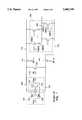
- FIG. 1is a schematic of a related memory sensing circuit
- FIGS. 2A-2Eare a timing diagram of the sensing circuit of FIG. 1;
- FIG. 3is a schematic of a sensing circuit of the present invention.
- FIGS. 4A-4Hare a timing diagram of the circuit in FIG. 3;
- FIGS. 5A-5Fare an alternate timing diagram of the circuit in FIG. 3;
- FIG. 6is a detailed diagram of a sensing and equilibration operation
- FIG. 7is a detailed diagram of an alternate equilibration operation
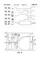
- FIG. 8is a simplified layout of a related memory circuit
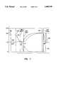
- FIG. 9is a simplified layout of a memory circuit incorporating the present invention.
- a memory array 100has a plurality of memory cells 102(0)-(n) which are fabricated as capacitors having one capacitive plate formed as a common cell plate 104 and the other node connected to an access transistor 106(0)-(n).
- Each access transistoris a n-type transistor having its gate connected to a word line 108(0)-(n).
- the cell plate 104is typically biased to one-half the power supply voltage (Vcc) by a biasing source (not shown).
- Digit lines 110 and 112are each connected to some of the access transistors and memory cells. When access transistors 106 are selectively activated, the charge stored on the corresponding memory cell 102 is coupled to one of the digit lines.
- N-type isolation transistors 114 and 116are used to isolate digit lines 110 and 112, respectively, from both the n-sense amp 118 and the p-sense amp 120.
- Equilibrate transistor 122is used to equalize the nodes of the sense amps to the same voltage, as described below.
- the first stepis to equilibrate nodes 129 and 131 of sense amps 118 and 120 to Vcc/2, as sourced by a biasing circuit (not shown), by holding the gate of transistor 122 (EQ) high.
- the differential voltage across the sense ampsis therefore zero with each node having a preferred voltage of one-half the supply voltage (Vcc).
- the next stepis to activate isolation transistors 114 and 116 by providing their gates (ISO A and ISO B, respectively) with a high voltage. This connects the digit lines 110 and 112 to the sense amps 118 and 120 and allows the digit lines to also stabilize to Vcc/2.
- One of the memory cell access transistors 106(0)-(n)is then selectively activated by raising the associated word line 108(0)-(n) gate voltage.
- the charge, or lack of charge, stored on the selected memory cell 102is then shared with one of the digit lines. If a logical "one" is stored on the capacitor the associated digit line will be slightly raised, for example by a voltage of approximately 100 mv. It will be understood that the charge shared with the digit line is directly dependant upon the charge stored on the memory cell. If the memory cell is un-charged the digit line voltage will drop, for example by 100 mv.
- n-sense amp 118 and the p-sense amp 120sense a differential between the digit lines and drive the digit lines to full rails in response.
- N-sense amp 118has two n-channel transistors having their gates cross-coupled to the source of the other transistor. The drains of each transistor are connected together and controlled by an NLat line.
- the NLat lineis typically pre-charged to the same level that nodes 129 and 131 have been equalized to, Vcc/2. The voltage on the NLat line is lowered to sense a high voltage on one of the nodes.
- transistor 119will begin to turn on when the NLat drops by a threshold voltage below node 129. Node 131 will then be pulled to NLat to insure that transistor 117 does not turn on.
- p-sense amp 120has two cross-coupled p-channel transistors 121 and 125. The drains of each transistor are connected together and controlled by a PLat line.
- the PLat lineis typically pre-charged to the same level that nodes 129 and 131 have been equalized to, Vcc/2. The voltage on the PLat line is raised to sense a low voltage on one of the nodes.
- transistor 121will begin to turn on when the PLat increases by a threshold voltage above node 131. Node 129 will then be pulled to PLat to insure that transistor 125 does not turn on.
- the NLat and PLatare strobed to full power rails, ground and Vcc, respectively. If one of the digit lines is higher, therefore, that digit line will be driven to Vcc while the complementary digit line is pulled to ground.
- the voltage on the digit linesare equal until shortly after the word line is activated.
- the n-sense ampis strobed first to drive one line low and then the p-sense amp is strobed to drive the other line high.
- the digit linesremain latched at these full power levels until the equilibrate transistor 122 is again activated.
- the memory cellis refreshed.
- FIG. 3illustrates a sensing circuit of the present invention.
- a memory array 123is comprised of memory cells 126(0)-(n) fabricated as capacitors with one node connected to a common cell plate 127. The cell plate is biased to one-half Vcc by a biasing circuit (not shown). The other plate of each memory cell 126 is connected to one of the n-type access transistors 128(0)-(n). The access transistors are connected to digit line 124 and have their gate connected one of the word lines 130(0)-(n).
- Isolation transistor 132is provided to selectively isolate digit line 124 from node 135 of both the n-sense amp 136 and the p-sense amp 138.
- n-type isolation/equilibrate transistor 134is connected between node 137 of the sense amps and the digit line 124.
- N-type equilibrate transistor 139is provided to equalize nodes 135 and 137 of the sense amps to a common voltage. As described below, this common voltage is preferably near Vcc/2.
- the digit line 124 and nodes 135 and 137 of the sense ampsare equalized by activating the gate of transistor 139 (EQ).
- Transistor 134is then turned off by lowering its gate voltage (ISO Equil).
- ISO Equilgate voltage
- the equilibrate transistor 139is turned off.
- the voltage at node 137is coupled down when transistor 139 is turned off.
- the voltage on node 137drops by approximately 20 mv when transistor 139 is turned off.
- Node 137is latched to the equilibrate voltage, less the coupling effect.
- One of the access transistors 128(0)-(n)is selectively activated by raising the corresponding word line 130(0)-(n).
- the charge, or lack of charge, stored in the memory cellis shared with the digit line and sense amp node 135.
- the change in the voltage on the digit lineis dependent upon the charge stored in the memory cell, typically this voltage differential, as stated above, is approximately ⁇ 100 mv.
- isolation transistor 132is turned off by lowering its gate voltage (ISO Digit) to isolate node 135 from the selected digit line.
- ISO Digitgate voltage
- the sense ampsare then strobed using NLat and PLat to drive node 135 to the appropriate supply level, as known to one skilled in the art. That is, if node 135 is above the equilibrate level, the node is driven to Vcc and if node 135 is below the equilibrate level it is driven to ground. Isolation transistor 132 is then re-activated by raising ISO Digit so that the entire digit line 124 can go to the appropriate power rail and the memory cell can be refreshed. After word line 130 returns to a low level, the equilibrate transistor can be re-activated to insure that both nodes of the sense amps and the digit line are equalized.
- transistor 134can be used to selectively connect node 137 to the digit line 124 to equilibrate the sense amps by forcing node 137 to an opposite state. That is, by first isolating node 135 from the digit line 124 and then activating transistor 134, the sense amps will force the voltage on the digit line to change its state. If, for example, the digit line is a "one" when transistor 134 is activated, the voltage on the digit line will be forced to transition low by the n-sense amp. It will be understood that by holding node 135 constant and using transistor 134, crossing currents are avoided.
- a trigger or tracking circuit(not shown) can be used to latch the voltage at a level near Vcc/2. One embodiment would be to use a timing circuit to turn on equilibrate transistor 139 and turn off sense amps 136 and 138.
- FIG. 5illustrates the timing of this alternate equilibrate circuit.
- Equilibrate transistor 139is turned off by lowering its gate voltage (EQ).
- Transistor 134is turned off by lowering its gate, ISO Equil.
- a word line 130is raised to access a memory cell 126 and transistor 132 is de-activated by lowering its gate voltage (ISO Digit).
- the sense ampsare strobed using NLat and PLat, and transistor 132 is re-activated to refresh the memory cell.
- transistor 132is turned off to isolate digit line 124 from node 135.
- Transistor 134is activated by raising its gate voltage (ISO Equil) and node 137 is connected to the digit line.
- the sense ampswill force the digit line to begin to change states by either charging or dis-charging the digit line.
- a timing or trigger circuitwill activate equilibrate transistor 139 and turn off the sense amps. Both nodes 135 and 137 are therefore equalized and transistors 132 is activated. Finally, transistor 134 is turned off.
- An optional bias circuit 141is shown in FIG. 3. This circuit can be used to bias the digit line 142 to a pre-determined voltage level. By activating transistors 132 and 139 the nodes of the sense amps could be equilibrated to the pre-determined voltage level. This equilibrate option requires additional die area and is therefore economically less desirable then the other equilibrate circuits.
- FIG. 6is a more detailed diagram of a sensing operation on a selected memory cell which contains data stored as a "one" in the circuit of FIG. 3. It can be seen that prior to the gate of transistor 139 (EQ) falling from Vcc (3.6 volts) the sense amp nodes 135 and 137 are equalized at 1.8 volts (Vcc/2). Node 137 is coupled low when EQ goes low, thereby, creating a small differential between nodes 135 and 137. One of the memory cells 126 is selected by raising its associated word line 130. The charge stored on the memory cell is shared with the digit line and node 135.
- the capacitance of the digit line 124is higher than the capacitance of the memory cell, thus the voltage of node 135 only increases by a fraction of the drop in voltage on the memory cell.
- Transistor 132is turned off by lowering the ISO Digit line. As a result, node 135 is coupled low and the differential voltage between the sense amp nodes reflects a true value of the memory cell charge.
- the n-sense amp 136is strobed (shown as point N) and then the p-sense amp 138 is strobed (shown as point P).
- node 135is coupled low after the n-sense amp is strobed, but is pulled high when the p-sense amp is strobed.
- Transistor 132is re-activated to connect node 135 to the digit line and memory cell 126. Both nodes of the sense amps are coupled high when the ISO Digit line goes high. Node 135 is pulled high by the p-sense amp and node 137 is pulled low by the n-sense amp.
- the memory cellis refreshed during the time that both transistor 132 and transistor 130 are activated. That is, the voltage on memory cell 126 is pulled to Vcc to re-charge the cell.
- transistors 132 and 130are connected to a pump voltage which has a high level above Vcc, as known to one skilled in the art.
- the EQ linereturns high to activate transistor 139 and nodes 135 and 137 are equilibrated to Vcc/2.
- FIG. 7is similar to FIG. 6, however, the sense amp nodes 135 and 137 are equilibrated using transistor 134. After the nodes have been driven to full rails by the sense amps, ISO Equil is raised to activate transistor 134. Node 137 is, therefore, initially coupled high and then begins to return low as the charge on the digit line is discharged. When the voltage level on node 137 is approximately Vcc/2 transistor 139 is activated and the sense amps are turned off to equilibrate nodes 135 and 137. The equilibrate voltage level can vary, provided the level remains approximately equal to the bias level of NLat and PLat.
- the related integrated circuituses two digit lines 140 to connect memory cells 142 to each sense amp 144.
- the memory cellsare arranged such that the intersection of every-other row line 146 and every-other digit line have a memory cell 142.
- Each sense amp 144can, therefore, selectively sense four different memory cells in this illustration. It can be seen that any reductions in memory cell size cannot be fully realized do to the layout spacing requirements.
- FIG. 9illustrates an integrated circuit incorporating the cell plate biasing of the present invention.
- Memory cells 150are located at each intersection of digit lines 148 and row lines 152.
- Sense amp circuits 154are biased using the single-ended circuit, as detailed above, and can selectively sense four different memory cells in this illustration.
- the present inventionallows the use 6F 2 size memory cells where the conventional circuit used 8F 2 memory cells, where F is the device feature size as known by one skilled in the art.
Landscapes
- Engineering & Computer Science (AREA)
- Microelectronics & Electronic Packaging (AREA)
- Computer Hardware Design (AREA)
- Dram (AREA)
- Semiconductor Memories (AREA)
Abstract
Description
Claims (15)
Priority Applications (1)
| Application Number | Priority Date | Filing Date | Title |
|---|---|---|---|
| US08/707,867US5684749A (en) | 1995-06-06 | 1996-09-09 | Single-ended sensing using global bit lines for dram |
Applications Claiming Priority (2)
| Application Number | Priority Date | Filing Date | Title |
|---|---|---|---|
| US08/471,860US5625588A (en) | 1995-06-06 | 1995-06-06 | Single-ended sensing using global bit lines for DRAM |
| US08/707,867US5684749A (en) | 1995-06-06 | 1996-09-09 | Single-ended sensing using global bit lines for dram |
Related Parent Applications (1)
| Application Number | Title | Priority Date | Filing Date |
|---|---|---|---|
| US08/471,860ContinuationUS5625588A (en) | 1995-06-06 | 1995-06-06 | Single-ended sensing using global bit lines for DRAM |
Publications (1)
| Publication Number | Publication Date |
|---|---|
| US5684749Atrue US5684749A (en) | 1997-11-04 |
Family
ID=23873265
Family Applications (2)
| Application Number | Title | Priority Date | Filing Date |
|---|---|---|---|
| US08/471,860Expired - LifetimeUS5625588A (en) | 1995-06-06 | 1995-06-06 | Single-ended sensing using global bit lines for DRAM |
| US08/707,867Expired - LifetimeUS5684749A (en) | 1995-06-06 | 1996-09-09 | Single-ended sensing using global bit lines for dram |
Family Applications Before (1)
| Application Number | Title | Priority Date | Filing Date |
|---|---|---|---|
| US08/471,860Expired - LifetimeUS5625588A (en) | 1995-06-06 | 1995-06-06 | Single-ended sensing using global bit lines for DRAM |
Country Status (9)
| Country | Link |
|---|---|
| US (2) | US5625588A (en) |
| EP (1) | EP0830685B1 (en) |
| JP (1) | JP3357899B2 (en) |
| KR (1) | KR100284468B1 (en) |
| AT (1) | ATE223614T1 (en) |
| AU (1) | AU6049196A (en) |
| DE (1) | DE69623466T2 (en) |
| TW (1) | TW300996B (en) |
| WO (1) | WO1996039699A1 (en) |
Cited By (8)
| Publication number | Priority date | Publication date | Assignee | Title |
|---|---|---|---|---|
| US5764562A (en)* | 1995-04-07 | 1998-06-09 | Mitsubishi Denki Kabushiki Kaisha | Semiconductor memory device |
| US5910920A (en)* | 1996-10-28 | 1999-06-08 | Micron Technology, Inc. | High speed input buffer |
| US5917758A (en)* | 1996-11-04 | 1999-06-29 | Micron Technology, Inc. | Adjustable output driver circuit |
| US6292417B1 (en) | 2000-07-26 | 2001-09-18 | Micron Technology, Inc. | Memory device with reduced bit line pre-charge voltage |
| US6301175B1 (en)* | 2000-07-26 | 2001-10-09 | Micron Technology, Inc. | Memory device with single-ended sensing and low voltage pre-charge |
| DE10110625A1 (en)* | 2001-03-06 | 2002-09-19 | Infineon Technologies Ag | Valuating read-out signal of read-out amplifier for dynamic semiconductor memory |
| US20070097768A1 (en)* | 2005-10-31 | 2007-05-03 | International Business Machines Corporation | System and method for capacitive mis-match bit-line sensing |
| WO2013075094A1 (en)* | 2011-11-17 | 2013-05-23 | Everspin Technologies Inc. | Write driver circuit and method for writing to a spin-torque mram |
Families Citing this family (10)
| Publication number | Priority date | Publication date | Assignee | Title |
|---|---|---|---|---|
| US5835433A (en)* | 1997-06-09 | 1998-11-10 | Micron Technology, Inc. | Floating isolation gate from DRAM sensing |
| US5862072A (en)* | 1997-08-22 | 1999-01-19 | Micron Technology, Inc. | Memory array architecture and method for dynamic cell plate sensing |
| US5949728A (en)* | 1997-12-12 | 1999-09-07 | Scenix Semiconductor, Inc. | High speed, noise immune, single ended sensing scheme for non-volatile memories |
| US6304809B1 (en) | 2000-03-21 | 2001-10-16 | Ford Global Technologies, Inc. | Engine control monitor for vehicle equipped with engine and transmission |
| ITRM20010001A1 (en)* | 2001-01-03 | 2002-07-03 | Micron Technology Inc | LOW VOLTAGE FLASH MEMORY DETECTION CIRCUIT. |
| US6822904B2 (en) | 2001-01-03 | 2004-11-23 | Micron Technology, Inc. | Fast sensing scheme for floating-gate memory cells |
| ITRM20010531A1 (en) | 2001-08-31 | 2003-02-28 | Micron Technology Inc | LOW POWER AND HIGH VOLTAGE DETECTOR DEVICE FOR DITIPO FLASH MEMORIES. |
| US7372092B2 (en)* | 2005-05-05 | 2008-05-13 | Micron Technology, Inc. | Memory cell, device, and system |
| US7196954B2 (en)* | 2005-06-06 | 2007-03-27 | Infineon Technologies Ag | Sensing current recycling method during self-refresh |
| US9847117B1 (en) | 2016-09-26 | 2017-12-19 | Micron Technology, Inc. | Dynamic reference voltage determination |
Citations (4)
| Publication number | Priority date | Publication date | Assignee | Title |
|---|---|---|---|---|
| US4715015A (en)* | 1984-06-01 | 1987-12-22 | Sharp Kabushiki Kaisha | Dynamic semiconductor memory with improved sense signal |
| US5241503A (en)* | 1991-02-25 | 1993-08-31 | Motorola, Inc. | Dynamic random access memory with improved page-mode performance and method therefor having isolator between memory cells and sense amplifiers |
| US5309392A (en)* | 1989-07-03 | 1994-05-03 | Hitachi, Ltd. | Semiconductor IC device using ferroelectric material in data storage cells with light assisted state transition |
| US5367481A (en)* | 1991-12-26 | 1994-11-22 | Kabushiki Kaisha Toshiba | Dynamic random access memory with complementary bit lines and capacitor common line |
Family Cites Families (11)
| Publication number | Priority date | Publication date | Assignee | Title |
|---|---|---|---|---|
| US4625300A (en)* | 1982-12-01 | 1986-11-25 | Texas Instruments Incorporated | Single-ended sense amplifier for dynamic memory array |
| US4598389A (en)* | 1984-10-01 | 1986-07-01 | Texas Instruments Incorporated | Single-ended CMOS sense amplifier |
| US4823031A (en)* | 1988-02-01 | 1989-04-18 | Texas Instruments Incorporated | Single-ended sense amplifier with positive feedback |
| US5042011A (en)* | 1989-05-22 | 1991-08-20 | Micron Technology, Inc. | Sense amplifier pulldown device with tailored edge input |
| US5013943A (en)* | 1989-08-11 | 1991-05-07 | Simtek Corporation | Single ended sense amplifier with improved data recall for variable bit line current |
| KR920000409B1 (en)* | 1989-11-30 | 1992-01-13 | 현대전자산업 주식회사 | Isoation circuit of dram |
| KR950009234B1 (en)* | 1992-02-19 | 1995-08-18 | 삼성전자주식회사 | Bit-line disconnection clock generating device of semiconductor memory device |
| US5220221A (en)* | 1992-03-06 | 1993-06-15 | Micron Technology, Inc. | Sense amplifier pulldown circuit for minimizing ground noise at high power supply voltages |
| US5369317A (en)* | 1992-06-26 | 1994-11-29 | Micron Technology, Inc. | Circuit and method for controlling the potential of a digit line and in limiting said potential to a maximum value |
| US5295100A (en)* | 1992-08-14 | 1994-03-15 | Micron Semiconductor, Inc. | Method for providing a faster ones voltage level restore operation in a DRAM |
| US5367213A (en)* | 1993-06-09 | 1994-11-22 | Micron Semiconductor, Inc. | P-channel sense amplifier pull-up circuit incorporating a voltage comparator for use in DRAM memories having non-bootstrapped word lines |
- 1995
- 1995-06-06USUS08/471,860patent/US5625588A/ennot_activeExpired - Lifetime
- 1996
- 1996-06-05WOPCT/US1996/009073patent/WO1996039699A1/enactiveIP Right Grant
- 1996-06-05JPJP50148197Apatent/JP3357899B2/ennot_activeExpired - Fee Related
- 1996-06-05AUAU60491/96Apatent/AU6049196A/ennot_activeAbandoned
- 1996-06-05DEDE69623466Tpatent/DE69623466T2/ennot_activeExpired - Lifetime
- 1996-06-05ATAT96918168Tpatent/ATE223614T1/ennot_activeIP Right Cessation
- 1996-06-05KRKR1019970709065Apatent/KR100284468B1/ennot_activeExpired - Fee Related
- 1996-06-05EPEP96918168Apatent/EP0830685B1/ennot_activeExpired - Lifetime
- 1996-06-13TWTW085107103Apatent/TW300996B/zhnot_activeIP Right Cessation
- 1996-09-09USUS08/707,867patent/US5684749A/ennot_activeExpired - Lifetime
Patent Citations (4)
| Publication number | Priority date | Publication date | Assignee | Title |
|---|---|---|---|---|
| US4715015A (en)* | 1984-06-01 | 1987-12-22 | Sharp Kabushiki Kaisha | Dynamic semiconductor memory with improved sense signal |
| US5309392A (en)* | 1989-07-03 | 1994-05-03 | Hitachi, Ltd. | Semiconductor IC device using ferroelectric material in data storage cells with light assisted state transition |
| US5241503A (en)* | 1991-02-25 | 1993-08-31 | Motorola, Inc. | Dynamic random access memory with improved page-mode performance and method therefor having isolator between memory cells and sense amplifiers |
| US5367481A (en)* | 1991-12-26 | 1994-11-22 | Kabushiki Kaisha Toshiba | Dynamic random access memory with complementary bit lines and capacitor common line |
Cited By (15)
| Publication number | Priority date | Publication date | Assignee | Title |
|---|---|---|---|---|
| US5764562A (en)* | 1995-04-07 | 1998-06-09 | Mitsubishi Denki Kabushiki Kaisha | Semiconductor memory device |
| US5910920A (en)* | 1996-10-28 | 1999-06-08 | Micron Technology, Inc. | High speed input buffer |
| US6326810B1 (en) | 1996-11-04 | 2001-12-04 | Micron Technology, Inc. | Adjustable output driver circuit |
| US5917758A (en)* | 1996-11-04 | 1999-06-29 | Micron Technology, Inc. | Adjustable output driver circuit |
| US6437600B1 (en) | 1996-11-04 | 2002-08-20 | Micron Technology, Inc. | Adjustable output driver circuit |
| US6292417B1 (en) | 2000-07-26 | 2001-09-18 | Micron Technology, Inc. | Memory device with reduced bit line pre-charge voltage |
| US6301175B1 (en)* | 2000-07-26 | 2001-10-09 | Micron Technology, Inc. | Memory device with single-ended sensing and low voltage pre-charge |
| DE10110625A1 (en)* | 2001-03-06 | 2002-09-19 | Infineon Technologies Ag | Valuating read-out signal of read-out amplifier for dynamic semiconductor memory |
| US20070097768A1 (en)* | 2005-10-31 | 2007-05-03 | International Business Machines Corporation | System and method for capacitive mis-match bit-line sensing |
| US7286425B2 (en)* | 2005-10-31 | 2007-10-23 | International Business Machines Corporation | System and method for capacitive mis-match bit-line sensing |
| WO2013075094A1 (en)* | 2011-11-17 | 2013-05-23 | Everspin Technologies Inc. | Write driver circuit and method for writing to a spin-torque mram |
| US8929132B2 (en) | 2011-11-17 | 2015-01-06 | Everspin Technologies, Inc. | Write driver circuit and method for writing to a spin-torque MRAM |
| US9378796B2 (en) | 2011-11-17 | 2016-06-28 | Everspin Technologies, Inc. | Method for writing to a magnetic tunnel junction device |
| US9734884B2 (en) | 2011-11-17 | 2017-08-15 | Everspin Technologies, Inc. | Method for writing to a magnetic tunnel junction device |
| CN104115228B (en)* | 2011-11-17 | 2017-08-25 | 艾沃思宾技术公司 | Writing driver circuit and method of writing spin-torque MRAM |
Also Published As
| Publication number | Publication date |
|---|---|
| DE69623466D1 (en) | 2002-10-10 |
| KR100284468B1 (en) | 2001-03-02 |
| ATE223614T1 (en) | 2002-09-15 |
| EP0830685B1 (en) | 2002-09-04 |
| EP0830685A1 (en) | 1998-03-25 |
| KR19990022584A (en) | 1999-03-25 |
| JP3357899B2 (en) | 2002-12-16 |
| WO1996039699A1 (en) | 1996-12-12 |
| JPH10507864A (en) | 1998-07-28 |
| TW300996B (en) | 1997-03-21 |
| AU6049196A (en) | 1996-12-24 |
| US5625588A (en) | 1997-04-29 |
| DE69623466T2 (en) | 2003-01-16 |
Similar Documents
| Publication | Publication Date | Title |
|---|---|---|
| US5636170A (en) | Low voltage dynamic memory | |
| US5608668A (en) | Dram wtih open digit lines and array edge reference sensing | |
| US4855628A (en) | Sense amplifier for high performance dram | |
| US5684749A (en) | Single-ended sensing using global bit lines for dram | |
| US5339274A (en) | Variable bitline precharge voltage sensing technique for DRAM structures | |
| JPH057796B2 (en) | ||
| US6728152B2 (en) | Sense amplifier for reduction of access device leakage | |
| US5255235A (en) | Dynamic random access memory with dummy word lines connected to bit line potential adjusting capacitors | |
| US4397003A (en) | Dynamic random access memory | |
| US6301175B1 (en) | Memory device with single-ended sensing and low voltage pre-charge | |
| KR20040008197A (en) | System and method for early write to memory by holding bitline at fixed potential | |
| US6295241B1 (en) | Dynamic random access memory device | |
| US6292417B1 (en) | Memory device with reduced bit line pre-charge voltage | |
| US5719813A (en) | Cell plate referencing for DRAM sensing | |
| US5831895A (en) | Dynamic cell plate sensing and equilibration in a memory device | |
| US5745423A (en) | Low power precharge circuit for a dynamic random access memory | |
| US6570799B1 (en) | Precharge and reference voltage technique for dynamic random access memories | |
| US6643214B2 (en) | Semiconductor memory device having write column select gate | |
| US20020015346A1 (en) | Dynamic random access memory device and process for controlling a read access of such a memory | |
| US20030123317A1 (en) | Semiconductor memory device having write column select gate |
Legal Events
| Date | Code | Title | Description |
|---|---|---|---|
| FEPP | Fee payment procedure | Free format text:PAYOR NUMBER ASSIGNED (ORIGINAL EVENT CODE: ASPN); ENTITY STATUS OF PATENT OWNER: LARGE ENTITY | |
| STCF | Information on status: patent grant | Free format text:PATENTED CASE | |
| FPAY | Fee payment | Year of fee payment:4 | |
| FPAY | Fee payment | Year of fee payment:8 | |
| FPAY | Fee payment | Year of fee payment:12 | |
| AS | Assignment | Owner name:U.S. BANK NATIONAL ASSOCIATION, AS COLLATERAL AGENT, CALIFORNIA Free format text:SECURITY INTEREST;ASSIGNOR:MICRON TECHNOLOGY, INC.;REEL/FRAME:038669/0001 Effective date:20160426 Owner name:U.S. BANK NATIONAL ASSOCIATION, AS COLLATERAL AGEN Free format text:SECURITY INTEREST;ASSIGNOR:MICRON TECHNOLOGY, INC.;REEL/FRAME:038669/0001 Effective date:20160426 | |
| AS | Assignment | Owner name:MORGAN STANLEY SENIOR FUNDING, INC., AS COLLATERAL AGENT, MARYLAND Free format text:PATENT SECURITY AGREEMENT;ASSIGNOR:MICRON TECHNOLOGY, INC.;REEL/FRAME:038954/0001 Effective date:20160426 Owner name:MORGAN STANLEY SENIOR FUNDING, INC., AS COLLATERAL Free format text:PATENT SECURITY AGREEMENT;ASSIGNOR:MICRON TECHNOLOGY, INC.;REEL/FRAME:038954/0001 Effective date:20160426 | |
| AS | Assignment | Owner name:U.S. BANK NATIONAL ASSOCIATION, AS COLLATERAL AGENT, CALIFORNIA Free format text:CORRECTIVE ASSIGNMENT TO CORRECT THE REPLACE ERRONEOUSLY FILED PATENT #7358718 WITH THE CORRECT PATENT #7358178 PREVIOUSLY RECORDED ON REEL 038669 FRAME 0001. ASSIGNOR(S) HEREBY CONFIRMS THE SECURITY INTEREST;ASSIGNOR:MICRON TECHNOLOGY, INC.;REEL/FRAME:043079/0001 Effective date:20160426 Owner name:U.S. BANK NATIONAL ASSOCIATION, AS COLLATERAL AGEN Free format text:CORRECTIVE ASSIGNMENT TO CORRECT THE REPLACE ERRONEOUSLY FILED PATENT #7358718 WITH THE CORRECT PATENT #7358178 PREVIOUSLY RECORDED ON REEL 038669 FRAME 0001. ASSIGNOR(S) HEREBY CONFIRMS THE SECURITY INTEREST;ASSIGNOR:MICRON TECHNOLOGY, INC.;REEL/FRAME:043079/0001 Effective date:20160426 | |
| AS | Assignment | Owner name:JPMORGAN CHASE BANK, N.A., AS COLLATERAL AGENT, ILLINOIS Free format text:SECURITY INTEREST;ASSIGNORS:MICRON TECHNOLOGY, INC.;MICRON SEMICONDUCTOR PRODUCTS, INC.;REEL/FRAME:047540/0001 Effective date:20180703 Owner name:JPMORGAN CHASE BANK, N.A., AS COLLATERAL AGENT, IL Free format text:SECURITY INTEREST;ASSIGNORS:MICRON TECHNOLOGY, INC.;MICRON SEMICONDUCTOR PRODUCTS, INC.;REEL/FRAME:047540/0001 Effective date:20180703 | |
| AS | Assignment | Owner name:MICRON TECHNOLOGY, INC., IDAHO Free format text:RELEASE BY SECURED PARTY;ASSIGNOR:U.S. BANK NATIONAL ASSOCIATION, AS COLLATERAL AGENT;REEL/FRAME:047243/0001 Effective date:20180629 | |
| AS | Assignment | Owner name:MICRON TECHNOLOGY, INC., IDAHO Free format text:RELEASE BY SECURED PARTY;ASSIGNOR:MORGAN STANLEY SENIOR FUNDING, INC., AS COLLATERAL AGENT;REEL/FRAME:050937/0001 Effective date:20190731 | |
| AS | Assignment | Owner name:MICRON SEMICONDUCTOR PRODUCTS, INC., IDAHO Free format text:RELEASE BY SECURED PARTY;ASSIGNOR:JPMORGAN CHASE BANK, N.A., AS COLLATERAL AGENT;REEL/FRAME:051028/0001 Effective date:20190731 Owner name:MICRON TECHNOLOGY, INC., IDAHO Free format text:RELEASE BY SECURED PARTY;ASSIGNOR:JPMORGAN CHASE BANK, N.A., AS COLLATERAL AGENT;REEL/FRAME:051028/0001 Effective date:20190731 |