US5683925A - Manufacturing method for ROM array with minimal band-to-band tunneling - Google Patents
Manufacturing method for ROM array with minimal band-to-band tunnelingDownload PDFInfo
- Publication number
- US5683925A US5683925AUS08/665,150US66515096AUS5683925AUS 5683925 AUS5683925 AUS 5683925AUS 66515096 AUS66515096 AUS 66515096AUS 5683925 AUS5683925 AUS 5683925A
- Authority
- US
- United States
- Prior art keywords
- rom
- core
- periphery
- area
- oxide layer
- Prior art date
- Legal status (The legal status is an assumption and is not a legal conclusion. Google has not performed a legal analysis and makes no representation as to the accuracy of the status listed.)
- Expired - Lifetime
Links
Images


Classifications
- H—ELECTRICITY
- H10—SEMICONDUCTOR DEVICES; ELECTRIC SOLID-STATE DEVICES NOT OTHERWISE PROVIDED FOR
- H10B—ELECTRONIC MEMORY DEVICES
- H10B20/00—Read-only memory [ROM] devices
- Y—GENERAL TAGGING OF NEW TECHNOLOGICAL DEVELOPMENTS; GENERAL TAGGING OF CROSS-SECTIONAL TECHNOLOGIES SPANNING OVER SEVERAL SECTIONS OF THE IPC; TECHNICAL SUBJECTS COVERED BY FORMER USPC CROSS-REFERENCE ART COLLECTIONS [XRACs] AND DIGESTS
- Y10—TECHNICAL SUBJECTS COVERED BY FORMER USPC
- Y10S—TECHNICAL SUBJECTS COVERED BY FORMER USPC CROSS-REFERENCE ART COLLECTIONS [XRACs] AND DIGESTS
- Y10S148/00—Metal treatment
- Y10S148/116—Oxidation, differential
- Y—GENERAL TAGGING OF NEW TECHNOLOGICAL DEVELOPMENTS; GENERAL TAGGING OF CROSS-SECTIONAL TECHNOLOGIES SPANNING OVER SEVERAL SECTIONS OF THE IPC; TECHNICAL SUBJECTS COVERED BY FORMER USPC CROSS-REFERENCE ART COLLECTIONS [XRACs] AND DIGESTS
- Y10—TECHNICAL SUBJECTS COVERED BY FORMER USPC
- Y10S—TECHNICAL SUBJECTS COVERED BY FORMER USPC CROSS-REFERENCE ART COLLECTIONS [XRACs] AND DIGESTS
- Y10S438/00—Semiconductor device manufacturing: process
- Y10S438/981—Utilizing varying dielectric thickness
Definitions
- the present inventionrelates to read only memory (ROM) arrays generally and to methods of manufacturing ROM arrays and to turning off selected ROM transistors without incurring significant, band-to-band leakage in particular.
- ROMread only memory
- ROM array chipsare very well known in the art.
- the chipsare formed of a ROM array core, comprising a multiplicity of ROM cells, and a periphery formed of control elements controlling the operation of the array core.
- the ROM arraystores programs and/or data in the form of bits, where a bit is either on (a logical value of 1) or off (a logical value of 0).
- a bitis either on (a logical value of 1) or off (a logical value of 0).
- Bach bitis stored in a single cell, which is a single gain, n-channel transistor or ROM cell.
- a logical 0is implemented with a transistor which has been shut off, such that it will not conduct when voltage is applied to it and a logical 1 is implemented with an active transistor which conducts when voltage is applied to it.
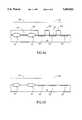
- FIG. 1illustrates a slice through a prior art ROM array chip showing one transistor 8 of the periphery, labeled 32, and two transistors 10 and 12 of the ROM array core, labeled 30, formed on a substrate 14.
- Transistor 8 and the other components of the peripheryare formed separately from the transistors 10 and 12 of the ROM array.
- Periphery transistor 8is formed of source and drain implants 4 and 5 and a polysilicon gate 20 and is surrounded by field oxide elements 6, which isolate transistor 8 from neighboring components.
- the gate 20is formed above a gate oxide layer 2.
- the size, shape and thickness of the elements of the periphery transistor 8may be determined, for example, by complementary metal oxide semiconductor (CMOS) periphery circuit requirements. For example, for a 0.8 ⁇ m CMOS technology, the gate oxide 2 is 150 ⁇ , the dose for the N + implant 5 is 4 ⁇ 10 15 atoms/cm 2 and the thickness of the field oxide 6 is 6000 ⁇ .
- CMOScomplementary
- the transistors 10 and 12are closer to each other than are neighboring components of the periphery. In fact, in the virtual ground ROM array of FIG. 1, the transistors 10 and 12 share diffusion bit lines 16 which act as the drain for one transistor and the source for the neighboring transistor. Between the bit lines 16, are channels 22. Other ROM architectures have the same problems as those described hereinbelow.
- bit line oxides 18Alocated on top of the bit lines 16, and gate oxides 18B, located on top of the channels 22 formed between the bit lines 16.
- the bit line oxides 18Aare typically thicker than the gate oxides 18B.
- the field oxide elements 6are much thicker than the bit line oxides 18A. For example, in 0.8 ⁇ m technology, the bit line oxides 18A are typically 1000 ⁇ and the field oxides 6 are typically 6000 ⁇ .
- Transistor 12additionally has a dopant 24 implanted into its channel 22.
- This dopantwhich is typically formed of Boron, raises the threshold voltage level Vth of the transistor 12 to above the standard activation voltage level such that, when the standard activation voltage is applied thereto, transistor 12 will not turn on.
- Transistor 12thus stores a logical 0. This is not true of transistor 10 which has no extra dopant in its channel 22 and therefore, has a low threshold voltage of about 0.8V. Thus, transistor 10, which stores a logical 1, will turn on when the standard activation voltage is applied thereto.
- the dopant 24is implanted into the channel 22 of transistor 12 during a ROM implant process. This process may occur, for example, after the polysilicon layer 20 has been laid down.
- the desired concentration of dopant 24is a function of the thickness of the gate oxide layer 18B, wherein the current trend is to reduce the thickness. The thinner the gate oxide layer 18B is, the higher the concentration of dopant 24 which is needed to bring the threshold voltage level Vth to close to the same voltage level. For example, if the desired voltage level is 5V, then a dose of 6 ⁇ 10 13 atoms/cm 2 of dopant is needed to produce a reasonable concentration (defined in atoms/cm 3 ) of dopant 24 for a gate oxide 18B of 150 ⁇ . Similarly, a dose of 3.5 ⁇ 10 13 atoms/cm 2 is needed for a gate oxide 18B of 250 ⁇ .
- the dopant 24when present in large quantities such that the concentration in the channel is a few times 10 18 atoms/cm 3 , it causes "band-to-band" tunneling of current I BB from the bit line 16 to the substrate 14 of the transistor 12. If this leakage current is large enough (for example, at a level of 30 ⁇ A per bit line or 30 nA per cell in a 1 Mbit array with 1000 transistors on a bit line or half of that for a 4 Mbit array), it will cause all "0"s on this bit line look as though they were conducting "1"s. Furthermore virtual ground arrays such as is shown in FIG. 1, this band-to-band tunneling current can cause a high standby current I SB . For example, for a 4 Mbit array, to maintain a standby current I SB of less than 1 ⁇ A , the maximum band-to-band tunneling current I BB per cell has to be less than 0.25 pA.
- FIG. 4illustrates the band-to-band tunneling current I BB versus the voltage V BL placed on the bit line.
- FIG. 4has four curves, 26, 27, 28 and 29, one for each of four channel implant doses, 5.5 ⁇ 10 13 , 9.0 ⁇ 10 13 , 12.5 ⁇ 10 13 and 16.0 ⁇ 10 13 , respectively.
- the curves 26-29indicate that, for any given dosage level, as the bit line voltage V BL increases, the band-to-band tunneling current I BB increases. Specifically, the current I BB increases by more than an order of magnitude in response to an increase of 1V in the bit line voltage. Furthermore, at a given voltage level, an increase in the implant level causes an increase of a few orders of magnitude, in the current I BB .
- the present inventiondescribes a method of manufacturing a ROM array to minimize band-to-band tunneling.
- the methodincludes the steps of: a) implanting bit lines into the core area of a substrate as per a later-removed bit line mask, b) providing a ROM oxide layer over the entirety of the substrate, c) etching the ROM oxide layer only from the periphery area as per a later-removed core protect mask, d) providing a gate oxide layer over the entirety of the ROM array, e) laying down polysilicon rows in the core area as per a polysilicon mask and f) implanting a ROM implant into selected areas of the core area, thereby to produce turned off core transistors.
- the methodalso includes the step of doping the periphery area to adjust the threshold level of only the periphery transistors therein.
- the step of dopingutilizes the core protect mask.
- the ROM arrayis a virtual ground array and the steps of providing oxide layers can be either deposition or oxidation steps.
- FIG. 1is a cross-sectional view of a slice of the ROM chip including two prior art ROM transistors, one which is on and one which is off and a periphery transistor;
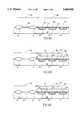
- FIGS. 5A and 5Bare cross-sectional views of a slice of a ROM array, constructed and operative in accordance with two alternative preferred embodiments of the present invention.
- FIGS. 6A, 6B, 6C, 6D, 6E, 6F and 6Gare cross-sectional views of the slice of FIG. 5 showing different stages of the manufacturing process.
- FIGS. 5A and 5Billustrate one slice of a ROM array, constructed and operative in accordance with two alternative preferred embodiments of the present invention, and to FIGS. 6A, 6B, 6C, 6D, 6E, 6F and 6G which illustrate the slice of FIGS. 5A and 5B at various stages during its manufacture.
- each ROM transistor 34 or 36is formed of the channel 22 between two neighboring bit lines 16, the gate oxide 18 above the channel 22 and the polysilicon layer 20 above the gate oxide 18. Furthermore, as in the prior art, the core bit line oxides, labeled 18D, are thicket than the core gate oxides, labeled 18C.
- the oxide layer 18 of the core area 30is thicker than the oxide layer 2 of the periphery 32.
- the periphery gate oxide 2might be 150 ⁇ thick
- the core gate oxide 18Cmight be 200 ⁇ thick
- the core bit line oxide 18Dmight be 1000 ⁇ thick or thicker.
- the amount of dopant 42 needed to shut off a core transistor 36is less than in the prior art. This is illustrated in FIGS. 5A and 5B where the dopant 42 is less dense than that of dopant 24 of FIG. 1.
- the percentage reduction in the amount of dopant 42 neededis directly proportional to the percentage increase in thickness of the core gate oxide 18C over the periphery gate oxide 2. For example, for a gate oxide 2 of 150 ⁇ , the dopant dose would be 6 ⁇ 10 13 atoms/cm 2 and for a gate oxide 18C of 250 ⁇ the dopant dose is reduced to 3.5 ⁇ 13 atoms/cm 2 .
- the present inventiondecouples the periphery gate oxide thickness from the core gate oxide thickness.
- the periphery gate oxide thicknessis determined by the requirements of the periphery circuitry and the core gate oxide thickness is determined by the desired low level of band-to-band tunneling current and the desired gate oxide breakdown level.
- the first process stepsare the standard initial CMOS/NMOS/PMOS/BICMOS process steps, including Nwell and field oxidation, thereby producing field oxide 6 of the periphery.
- the ROM array processbegins with a screen oxide 61 (FIG. 6A) over the entire chip, where the screen oxide 61 typically is grown to about 200 ⁇ . It is noted that, as a result of the screen oxidation operation, the field oxides 6 become thicker, as shown.
- bit line implant operationthe resist 63 and screen oxide 61 are removed, leaving a clear substrate surface in the core area 30 and slightly thinner field oxides 6 in the periphery area 32, as shown in FIG. 6B.
- a threshold adjustment operationis then performed on the entire array to ensure that every ROM transistor 34 and 36 has a desired threshold level, typically of 0.6-1.0V. This operation also provides an initial threshold level for the periphery transistors 38.
- a core protect mask 66(FIG. 6D) is now laid down on the core area 30 to protect the core while the ROM oxide layer 64 is removed from the periphery with a wet etch.
- the oxide layers and 67remain on the core 30 but the oxide layer 64 is removed from the periphery
- core protect mask 66is further utilized perform a further threshold adjustment operation, in which implant 40 is implanted, as illustrated in FIG. 6E.
- Implant 40adjusts the threshold level of the periphery transistor 38 to the desired level for the periphery transistors. This step can be performed either before or after the wet etch of the ROM oxide layer 64.
- FIG. 6Fshows the results of the gate oxidation for the array of FIG. 6D
- FIG. 6Gshows the results for the alternative array of FIG. 6E.
- the gate oxidation stepproduces the periphery gate oxide 2 between the field oxides 6 of the periphery area 32 and increases the thickness of the oxide layers 65 and 67 of the core area 30, therby to produce the bit line oxide 18D and the core gate oxide 18C, respectively.
- a suitable gate oxidation cycleis selected and a suitable thickness, such as 150 ⁇ is chosen to conform to the CMOS/NMOS/PMOS/BICMOS circuit requirements of the periphery area 32.
- the precursor bit lines 16'are also deepened during this process, there by becoming the bit lines 16.
- the processing of the arraycontinues as in the prior art and includes laying down word lines 20 of polysilicon. At this point, the n-channel transistors 34 and 36 have been formed, but they are all on. A ROM implant mask is then laid down to protect those ROM transistors 34 which are to remain on as well as the entirety of the periphery 32. A ROM implant, typically of Boron B 11 , is performed, implanting Boron into the ROM transistors 36, thereby shutting them off. The result is shown in FIG. 5A for the array without the implant 40 and in FIG. 5B for the array with the implant 40.
- the amount of ROM implant to be implantedis the amount necessary to raise the threshold voltage Vth of the off transistors 36 from the threshold level defined by the extra thick core gate oxides 18C to the shut off threshold volume level (e.g. 5V). This around of implant is less than in the prior art since the thicker gate oxide 18C provides a higher basic threshold voltage.
- the criticality of using less Boronis that it reduces the band-to-band associated leakage current and other undesirable phenomena.
- the remaining process stepsare the standard POM backend processing steps and include metallization and passivation.
- the present inventioncan be implemented for non-virtual ground arrays, for p-channel transistors and for deposition type oxidation operations.
Landscapes
- Semiconductor Memories (AREA)
Abstract
Description
Claims (9)
Priority Applications (1)
| Application Number | Priority Date | Filing Date | Title |
|---|---|---|---|
| US08/665,150US5683925A (en) | 1996-06-13 | 1996-06-13 | Manufacturing method for ROM array with minimal band-to-band tunneling |
Applications Claiming Priority (1)
| Application Number | Priority Date | Filing Date | Title |
|---|---|---|---|
| US08/665,150US5683925A (en) | 1996-06-13 | 1996-06-13 | Manufacturing method for ROM array with minimal band-to-band tunneling |
Publications (1)
| Publication Number | Publication Date |
|---|---|
| US5683925Atrue US5683925A (en) | 1997-11-04 |
Family
ID=24668933
Family Applications (1)
| Application Number | Title | Priority Date | Filing Date |
|---|---|---|---|
| US08/665,150Expired - LifetimeUS5683925A (en) | 1996-06-13 | 1996-06-13 | Manufacturing method for ROM array with minimal band-to-band tunneling |
Country Status (1)
| Country | Link |
|---|---|
| US (1) | US5683925A (en) |
Cited By (51)
| Publication number | Priority date | Publication date | Assignee | Title |
|---|---|---|---|---|
| US5970348A (en)* | 1996-10-31 | 1999-10-19 | Sgs-Thomson Microelectronics S.A. | Read-only memory and corresponding method of manufacturing by MOS technology |
| US6033943A (en)* | 1996-08-23 | 2000-03-07 | Advanced Micro Devices, Inc. | Dual gate oxide thickness integrated circuit and process for making same |
| US6037225A (en)* | 1998-04-14 | 2000-03-14 | Texas Instruments Acer Incorporated | Manufacturing method for mask ROM devices |
| US6037224A (en)* | 1997-05-02 | 2000-03-14 | Advanced Micro Devices, Inc. | Method for growing dual oxide thickness using nitrided oxides for oxidation suppression |
| US6051510A (en)* | 1997-05-02 | 2000-04-18 | Advanced Micro Devices, Inc. | Method of using a hard mask to grow dielectrics with varying characteristics |
| US6091119A (en)* | 1998-07-10 | 2000-07-18 | Acer Semiconductor Manufacturing Inc. | Double poly-gate high density multi-state flat mask ROM cells |
| US6118160A (en)* | 1998-06-01 | 2000-09-12 | Texas Instruments - Acer Incorporated | Structure of a mask ROM device on a semiconductor substrate having a cell area for coding |
| US6133102A (en)* | 1998-06-19 | 2000-10-17 | Wu; Shye-Lin | Method of fabricating double poly-gate high density multi-state flat mask ROM cells |
| US6200861B1 (en)* | 1999-03-26 | 2001-03-13 | Taiwan Semiconductor Manufacturing Co., Ltd. | Method of fabricating high density multiple states mask ROM cells |
| US6201282B1 (en) | 1998-05-05 | 2001-03-13 | Saifun Semiconductors Ltd. | Two bit ROM cell and process for producing same |
| US6297102B1 (en) | 1999-10-01 | 2001-10-02 | Taiwan Semiconductor Manufacturing Company | Method of forming a surface implant region on a ROM cell using a PLDD implant |
| US6430077B1 (en) | 1997-12-12 | 2002-08-06 | Saifun Semiconductors Ltd. | Method for regulating read voltage level at the drain of a cell in a symmetric array |
| US20030117861A1 (en)* | 2001-12-20 | 2003-06-26 | Eduardo Maayan | NROM NOR array |
| US20030142544A1 (en)* | 2002-01-31 | 2003-07-31 | Eduardo Maayan | Mass storage array and methods for operation thereof |
| US6614692B2 (en) | 2001-01-18 | 2003-09-02 | Saifun Semiconductors Ltd. | EEPROM array and method for operation thereof |
| US6633496B2 (en) | 1997-12-12 | 2003-10-14 | Saifun Semiconductors Ltd. | Symmetric architecture for memory cells having widely spread metal bit lines |
| US6633499B1 (en) | 1997-12-12 | 2003-10-14 | Saifun Semiconductors Ltd. | Method for reducing voltage drops in symmetric array architectures |
| US6636440B2 (en) | 2001-04-25 | 2003-10-21 | Saifun Semiconductors Ltd. | Method for operation of an EEPROM array, including refresh thereof |
| US6643181B2 (en) | 2001-10-24 | 2003-11-04 | Saifun Semiconductors Ltd. | Method for erasing a memory cell |
| US6677805B2 (en) | 2001-04-05 | 2004-01-13 | Saifun Semiconductors Ltd. | Charge pump stage with body effect minimization |
| US6803299B2 (en) | 1997-07-30 | 2004-10-12 | Saifun Semiconductors Ltd. | Non-volatile electrically erasable and programmable semiconductor memory cell utilizing asymmetrical charge trapping |
| US6826107B2 (en) | 2002-08-01 | 2004-11-30 | Saifun Semiconductors Ltd. | High voltage insertion in flash memory cards |
| US20040241926A1 (en)* | 2002-08-26 | 2004-12-02 | Jhyy-Cheng Liou | Contactless mask progammable rom |
| US6829172B2 (en) | 2000-05-04 | 2004-12-07 | Saifun Semiconductors Ltd. | Programming of nonvolatile memory cells |
| US6917544B2 (en) | 2002-07-10 | 2005-07-12 | Saifun Semiconductors Ltd. | Multiple use memory chip |
| US6928001B2 (en) | 2000-12-07 | 2005-08-09 | Saifun Semiconductors Ltd. | Programming and erasing methods for a non-volatile memory cell |
| WO2005029545A3 (en)* | 2003-09-15 | 2005-11-03 | Ibm | Self-aligned planar double-gate process by self-aligned oxidation |
| US7116577B2 (en) | 1997-08-01 | 2006-10-03 | Saifun Semiconductors Ltd | Two bit non-volatile electrically erasable and programmable semiconductor memory cell utilizing asymmetrical charge trapping |
| US7221138B2 (en) | 2005-09-27 | 2007-05-22 | Saifun Semiconductors Ltd | Method and apparatus for measuring charge pump output current |
| US7317633B2 (en) | 2004-07-06 | 2008-01-08 | Saifun Semiconductors Ltd | Protection of NROM devices from charge damage |
| US7352627B2 (en) | 2006-01-03 | 2008-04-01 | Saifon Semiconductors Ltd. | Method, system, and circuit for operating a non-volatile memory array |
| US7369440B2 (en) | 2005-01-19 | 2008-05-06 | Saifun Semiconductors Ltd. | Method, circuit and systems for erasing one or more non-volatile memory cells |
| US7420848B2 (en) | 2002-01-31 | 2008-09-02 | Saifun Semiconductors Ltd. | Method, system, and circuit for operating a non-volatile memory array |
| US7457183B2 (en) | 2003-09-16 | 2008-11-25 | Saifun Semiconductors Ltd. | Operating array cells with matched reference cells |
| US7466594B2 (en) | 2004-08-12 | 2008-12-16 | Saifun Semiconductors Ltd. | Dynamic matching of signal path and reference path for sensing |
| US7512009B2 (en) | 2001-04-05 | 2009-03-31 | Saifun Semiconductors Ltd. | Method for programming a reference cell |
| US7532529B2 (en) | 2004-03-29 | 2009-05-12 | Saifun Semiconductors Ltd. | Apparatus and methods for multi-level sensing in a memory array |
| US7535765B2 (en) | 2004-12-09 | 2009-05-19 | Saifun Semiconductors Ltd. | Non-volatile memory device and method for reading cells |
| US7605579B2 (en) | 2006-09-18 | 2009-10-20 | Saifun Semiconductors Ltd. | Measuring and controlling current consumption and output current of charge pumps |
| US7638835B2 (en) | 2006-02-28 | 2009-12-29 | Saifun Semiconductors Ltd. | Double density NROM with nitride strips (DDNS) |
| US7638850B2 (en) | 2004-10-14 | 2009-12-29 | Saifun Semiconductors Ltd. | Non-volatile memory structure and method of fabrication |
| US7668017B2 (en) | 2005-08-17 | 2010-02-23 | Saifun Semiconductors Ltd. | Method of erasing non-volatile memory cells |
| US7675782B2 (en) | 2002-10-29 | 2010-03-09 | Saifun Semiconductors Ltd. | Method, system and circuit for programming a non-volatile memory array |
| US7692961B2 (en) | 2006-02-21 | 2010-04-06 | Saifun Semiconductors Ltd. | Method, circuit and device for disturb-control of programming nonvolatile memory cells by hot-hole injection (HHI) and by channel hot-electron (CHE) injection |
| US7701779B2 (en) | 2006-04-27 | 2010-04-20 | Sajfun Semiconductors Ltd. | Method for programming a reference cell |
| US7743230B2 (en) | 2003-01-31 | 2010-06-22 | Saifun Semiconductors Ltd. | Memory array programming circuit and a method for using the circuit |
| US7760554B2 (en) | 2006-02-21 | 2010-07-20 | Saifun Semiconductors Ltd. | NROM non-volatile memory and mode of operation |
| US7786512B2 (en) | 2005-07-18 | 2010-08-31 | Saifun Semiconductors Ltd. | Dense non-volatile memory array and method of fabrication |
| US7808818B2 (en) | 2006-01-12 | 2010-10-05 | Saifun Semiconductors Ltd. | Secondary injection for NROM |
| US8053812B2 (en) | 2005-03-17 | 2011-11-08 | Spansion Israel Ltd | Contact in planar NROM technology |
| US8253452B2 (en) | 2006-02-21 | 2012-08-28 | Spansion Israel Ltd | Circuit and method for powering up an integrated circuit and an integrated circuit utilizing same |
Citations (4)
| Publication number | Priority date | Publication date | Assignee | Title |
|---|---|---|---|---|
| US5308781A (en)* | 1990-05-21 | 1994-05-03 | Ricoh Company, Ltd. | Semiconductor memory device |
| US5470774A (en)* | 1993-10-08 | 1995-11-28 | Nec Corporation | Fabrication method of a read-only semiconductor memory device |
| US5504030A (en)* | 1995-07-21 | 1996-04-02 | United Microelectronics Corporation | Process for fabricating high-density mask ROM devices |
| US5580809A (en)* | 1991-02-19 | 1996-12-03 | Mitsubishi Denki Kabushiki Kaisha | Method of making a mask ROM using tunnel current detection to store data |
- 1996
- 1996-06-13USUS08/665,150patent/US5683925A/ennot_activeExpired - Lifetime
Patent Citations (4)
| Publication number | Priority date | Publication date | Assignee | Title |
|---|---|---|---|---|
| US5308781A (en)* | 1990-05-21 | 1994-05-03 | Ricoh Company, Ltd. | Semiconductor memory device |
| US5580809A (en)* | 1991-02-19 | 1996-12-03 | Mitsubishi Denki Kabushiki Kaisha | Method of making a mask ROM using tunnel current detection to store data |
| US5470774A (en)* | 1993-10-08 | 1995-11-28 | Nec Corporation | Fabrication method of a read-only semiconductor memory device |
| US5504030A (en)* | 1995-07-21 | 1996-04-02 | United Microelectronics Corporation | Process for fabricating high-density mask ROM devices |
Cited By (62)
| Publication number | Priority date | Publication date | Assignee | Title |
|---|---|---|---|---|
| US6033943A (en)* | 1996-08-23 | 2000-03-07 | Advanced Micro Devices, Inc. | Dual gate oxide thickness integrated circuit and process for making same |
| US5970348A (en)* | 1996-10-31 | 1999-10-19 | Sgs-Thomson Microelectronics S.A. | Read-only memory and corresponding method of manufacturing by MOS technology |
| US6037224A (en)* | 1997-05-02 | 2000-03-14 | Advanced Micro Devices, Inc. | Method for growing dual oxide thickness using nitrided oxides for oxidation suppression |
| US6051510A (en)* | 1997-05-02 | 2000-04-18 | Advanced Micro Devices, Inc. | Method of using a hard mask to grow dielectrics with varying characteristics |
| US6803299B2 (en) | 1997-07-30 | 2004-10-12 | Saifun Semiconductors Ltd. | Non-volatile electrically erasable and programmable semiconductor memory cell utilizing asymmetrical charge trapping |
| US7405969B2 (en) | 1997-08-01 | 2008-07-29 | Saifun Semiconductors Ltd. | Non-volatile memory cell and non-volatile memory devices |
| US7116577B2 (en) | 1997-08-01 | 2006-10-03 | Saifun Semiconductors Ltd | Two bit non-volatile electrically erasable and programmable semiconductor memory cell utilizing asymmetrical charge trapping |
| US6430077B1 (en) | 1997-12-12 | 2002-08-06 | Saifun Semiconductors Ltd. | Method for regulating read voltage level at the drain of a cell in a symmetric array |
| US6633499B1 (en) | 1997-12-12 | 2003-10-14 | Saifun Semiconductors Ltd. | Method for reducing voltage drops in symmetric array architectures |
| US6633496B2 (en) | 1997-12-12 | 2003-10-14 | Saifun Semiconductors Ltd. | Symmetric architecture for memory cells having widely spread metal bit lines |
| US6037225A (en)* | 1998-04-14 | 2000-03-14 | Texas Instruments Acer Incorporated | Manufacturing method for mask ROM devices |
| US6201282B1 (en) | 1998-05-05 | 2001-03-13 | Saifun Semiconductors Ltd. | Two bit ROM cell and process for producing same |
| US6118160A (en)* | 1998-06-01 | 2000-09-12 | Texas Instruments - Acer Incorporated | Structure of a mask ROM device on a semiconductor substrate having a cell area for coding |
| US6133102A (en)* | 1998-06-19 | 2000-10-17 | Wu; Shye-Lin | Method of fabricating double poly-gate high density multi-state flat mask ROM cells |
| US6091119A (en)* | 1998-07-10 | 2000-07-18 | Acer Semiconductor Manufacturing Inc. | Double poly-gate high density multi-state flat mask ROM cells |
| US6200861B1 (en)* | 1999-03-26 | 2001-03-13 | Taiwan Semiconductor Manufacturing Co., Ltd. | Method of fabricating high density multiple states mask ROM cells |
| US6297102B1 (en) | 1999-10-01 | 2001-10-02 | Taiwan Semiconductor Manufacturing Company | Method of forming a surface implant region on a ROM cell using a PLDD implant |
| US6937521B2 (en) | 2000-05-04 | 2005-08-30 | Saifun Semiconductors Ltd. | Programming and erasing methods for a non-volatile memory cell |
| US6829172B2 (en) | 2000-05-04 | 2004-12-07 | Saifun Semiconductors Ltd. | Programming of nonvolatile memory cells |
| US6928001B2 (en) | 2000-12-07 | 2005-08-09 | Saifun Semiconductors Ltd. | Programming and erasing methods for a non-volatile memory cell |
| US6614692B2 (en) | 2001-01-18 | 2003-09-02 | Saifun Semiconductors Ltd. | EEPROM array and method for operation thereof |
| US7518908B2 (en) | 2001-01-18 | 2009-04-14 | Saifun Semiconductors Ltd. | EEPROM array and method for operation thereof |
| US6864739B2 (en) | 2001-04-05 | 2005-03-08 | Saifun Semiconductors Ltd. | Charge pump stage with body effect minimization |
| US6677805B2 (en) | 2001-04-05 | 2004-01-13 | Saifun Semiconductors Ltd. | Charge pump stage with body effect minimization |
| US7512009B2 (en) | 2001-04-05 | 2009-03-31 | Saifun Semiconductors Ltd. | Method for programming a reference cell |
| US20040130385A1 (en)* | 2001-04-05 | 2004-07-08 | Shor Joseph S. | Charge pump stage with body effect minimization |
| US6636440B2 (en) | 2001-04-25 | 2003-10-21 | Saifun Semiconductors Ltd. | Method for operation of an EEPROM array, including refresh thereof |
| US6643181B2 (en) | 2001-10-24 | 2003-11-04 | Saifun Semiconductors Ltd. | Method for erasing a memory cell |
| US6888757B2 (en) | 2001-10-24 | 2005-05-03 | Saifun Semiconductors Ltd. | Method for erasing a memory cell |
| US6885585B2 (en) | 2001-12-20 | 2005-04-26 | Saifun Semiconductors Ltd. | NROM NOR array |
| US20030117861A1 (en)* | 2001-12-20 | 2003-06-26 | Eduardo Maayan | NROM NOR array |
| US7420848B2 (en) | 2002-01-31 | 2008-09-02 | Saifun Semiconductors Ltd. | Method, system, and circuit for operating a non-volatile memory array |
| US6975536B2 (en) | 2002-01-31 | 2005-12-13 | Saifun Semiconductors Ltd. | Mass storage array and methods for operation thereof |
| US20030142544A1 (en)* | 2002-01-31 | 2003-07-31 | Eduardo Maayan | Mass storage array and methods for operation thereof |
| US7738304B2 (en) | 2002-07-10 | 2010-06-15 | Saifun Semiconductors Ltd. | Multiple use memory chip |
| US6917544B2 (en) | 2002-07-10 | 2005-07-12 | Saifun Semiconductors Ltd. | Multiple use memory chip |
| US6826107B2 (en) | 2002-08-01 | 2004-11-30 | Saifun Semiconductors Ltd. | High voltage insertion in flash memory cards |
| US20040241926A1 (en)* | 2002-08-26 | 2004-12-02 | Jhyy-Cheng Liou | Contactless mask progammable rom |
| US7675782B2 (en) | 2002-10-29 | 2010-03-09 | Saifun Semiconductors Ltd. | Method, system and circuit for programming a non-volatile memory array |
| US7743230B2 (en) | 2003-01-31 | 2010-06-22 | Saifun Semiconductors Ltd. | Memory array programming circuit and a method for using the circuit |
| WO2005029545A3 (en)* | 2003-09-15 | 2005-11-03 | Ibm | Self-aligned planar double-gate process by self-aligned oxidation |
| US7457183B2 (en) | 2003-09-16 | 2008-11-25 | Saifun Semiconductors Ltd. | Operating array cells with matched reference cells |
| US7532529B2 (en) | 2004-03-29 | 2009-05-12 | Saifun Semiconductors Ltd. | Apparatus and methods for multi-level sensing in a memory array |
| US7317633B2 (en) | 2004-07-06 | 2008-01-08 | Saifun Semiconductors Ltd | Protection of NROM devices from charge damage |
| US7466594B2 (en) | 2004-08-12 | 2008-12-16 | Saifun Semiconductors Ltd. | Dynamic matching of signal path and reference path for sensing |
| US7964459B2 (en) | 2004-10-14 | 2011-06-21 | Spansion Israel Ltd. | Non-volatile memory structure and method of fabrication |
| US7638850B2 (en) | 2004-10-14 | 2009-12-29 | Saifun Semiconductors Ltd. | Non-volatile memory structure and method of fabrication |
| US7535765B2 (en) | 2004-12-09 | 2009-05-19 | Saifun Semiconductors Ltd. | Non-volatile memory device and method for reading cells |
| US7468926B2 (en) | 2005-01-19 | 2008-12-23 | Saifun Semiconductors Ltd. | Partial erase verify |
| US7369440B2 (en) | 2005-01-19 | 2008-05-06 | Saifun Semiconductors Ltd. | Method, circuit and systems for erasing one or more non-volatile memory cells |
| US8053812B2 (en) | 2005-03-17 | 2011-11-08 | Spansion Israel Ltd | Contact in planar NROM technology |
| US7786512B2 (en) | 2005-07-18 | 2010-08-31 | Saifun Semiconductors Ltd. | Dense non-volatile memory array and method of fabrication |
| US7668017B2 (en) | 2005-08-17 | 2010-02-23 | Saifun Semiconductors Ltd. | Method of erasing non-volatile memory cells |
| US7221138B2 (en) | 2005-09-27 | 2007-05-22 | Saifun Semiconductors Ltd | Method and apparatus for measuring charge pump output current |
| US7352627B2 (en) | 2006-01-03 | 2008-04-01 | Saifon Semiconductors Ltd. | Method, system, and circuit for operating a non-volatile memory array |
| US7808818B2 (en) | 2006-01-12 | 2010-10-05 | Saifun Semiconductors Ltd. | Secondary injection for NROM |
| US7692961B2 (en) | 2006-02-21 | 2010-04-06 | Saifun Semiconductors Ltd. | Method, circuit and device for disturb-control of programming nonvolatile memory cells by hot-hole injection (HHI) and by channel hot-electron (CHE) injection |
| US7760554B2 (en) | 2006-02-21 | 2010-07-20 | Saifun Semiconductors Ltd. | NROM non-volatile memory and mode of operation |
| US8253452B2 (en) | 2006-02-21 | 2012-08-28 | Spansion Israel Ltd | Circuit and method for powering up an integrated circuit and an integrated circuit utilizing same |
| US7638835B2 (en) | 2006-02-28 | 2009-12-29 | Saifun Semiconductors Ltd. | Double density NROM with nitride strips (DDNS) |
| US7701779B2 (en) | 2006-04-27 | 2010-04-20 | Sajfun Semiconductors Ltd. | Method for programming a reference cell |
| US7605579B2 (en) | 2006-09-18 | 2009-10-20 | Saifun Semiconductors Ltd. | Measuring and controlling current consumption and output current of charge pumps |
Similar Documents
| Publication | Publication Date | Title |
|---|---|---|
| US5683925A (en) | Manufacturing method for ROM array with minimal band-to-band tunneling | |
| US5942780A (en) | Integrated circuit having, and process providing, different oxide layer thicknesses on a substrate | |
| US5156990A (en) | Floating-gate memory cell with tailored doping profile | |
| US5672521A (en) | Method of forming multiple gate oxide thicknesses on a wafer substrate | |
| US7638401B2 (en) | Memory device with surface-channel peripheral transistors | |
| US5644533A (en) | Flash memory system, and methods of constructing and utilizing same | |
| US5091324A (en) | Process for producing optimum intrinsic, long channel, and short channel mos devices in vlsi structures | |
| JPH0786530A (en) | Alternate metal/source virtually grounding type flash eprom cell array | |
| JP2001313374A (en) | Method for manufacturing integrated circuit integrating electrically programmable nonvolatile memory and high performance logic circuit net in identical semiconductor chip | |
| US6730555B2 (en) | Transistors having selectively doped channel regions | |
| US5604150A (en) | Channel-stop process for use with thick-field isolation regions in triple-well structures | |
| US20020014642A1 (en) | Independently programmable memory segments within a PMOS electrically erasable programmable read only memory array achieved by N-well separation and method therefor | |
| US6362049B1 (en) | High yield performance semiconductor process flow for NAND flash memory products | |
| JPH03245566A (en) | Non-volatile semiconductor memory device | |
| US6495896B1 (en) | Semiconductor integrated circuit device with high and low voltage wells | |
| US4342100A (en) | Implant programmable metal gate MOS read only memory | |
| US6177313B1 (en) | Method for forming a muti-level ROM memory in a dual gate CMOS process, and corresponding ROM memory cell | |
| US4535530A (en) | Process for manufacturing a semiconductor memory device | |
| US4979005A (en) | Floating-gate memory cell with tailored doping profile | |
| US7005342B2 (en) | Method to fabricate surface p-channel CMOS | |
| KR19990049409A (en) | How to Form Gate Oxides of Different Thickness | |
| US4336647A (en) | Method of making implant programmable N-channel read only memory | |
| US6156610A (en) | Process for manufacturing an EEPROM having a peripheral transistor with thick oxide | |
| US5036375A (en) | Floating-gate memory cell with tailored doping profile | |
| KR100513445B1 (en) | Method for manufacturing semiconductor device |
Legal Events
| Date | Code | Title | Description |
|---|---|---|---|
| AS | Assignment | Owner name:AMERICAN MICROSYSTEMS, INC., IDAHO Free format text:A CORRECTIVE ASSIGNMENT TO CORRECT AN INCORRECT SN 08/655150 ON REEL 8306 FRAME 0001;ASSIGNORS:IRANI, RUSTOM F.;KAZEROUNIAN, REZA;NELSON, MARK MICHAEL;REEL/FRAME:008444/0145;SIGNING DATES FROM 19960930 TO 19961022 Owner name:WAFERSCALE INTEGRATION INC., CALIFORNIA Free format text:A CORRECTIVE ASSIGNMENT TO CORRECT AN INCORRECT SN 08/655150 ON REEL 8306 FRAME 0001;ASSIGNORS:IRANI, RUSTOM F.;KAZEROUNIAN, REZA;NELSON, MARK MICHAEL;REEL/FRAME:008444/0145;SIGNING DATES FROM 19960930 TO 19961022 | |
| STCF | Information on status: patent grant | Free format text:PATENTED CASE | |
| AS | Assignment | Owner name:AMERICAN MICROSYSTEMS HOLDING CORPORATION, IDAHO Free format text:MERGER;ASSIGNOR:AMERICAN MICROSYSTEMS, INC.;REEL/FRAME:011277/0491 Effective date:19970725 Owner name:GA-TEK INC., OHIO Free format text:MERGER AND CHANGE OF NAME;ASSIGNOR:AMERICAN MICROSYSTEMS HOLDING CORPORATION;REEL/FRAME:011277/0509 Effective date:19980101 | |
| FEPP | Fee payment procedure | Free format text:PAYOR NUMBER ASSIGNED (ORIGINAL EVENT CODE: ASPN); ENTITY STATUS OF PATENT OWNER: LARGE ENTITY | |
| AS | Assignment | Owner name:AMI SPINCO, INC., IDAHO Free format text:ASSIGNMENT OF ASSIGNORS INTEREST;ASSIGNOR:GA-TEK, INC.;REEL/FRAME:011369/0264 Effective date:20000729 | |
| AS | Assignment | Owner name:CREDIT SUISSE FIRST BOSTON, AS COLLATERAL AGENT, N Free format text:SECURITY INTEREST;ASSIGNOR:AMI SPINCO, INC.;REEL/FRAME:011457/0562 Effective date:20001221 | |
| AS | Assignment | Owner name:AMI SEMICONDUCTOR, INC., IDAHO Free format text:MERGER/CHANGE OF NAME;ASSIGNOR:AMI SPINCO, INC.;REEL/FRAME:011601/0413 Effective date:20001221 | |
| FPAY | Fee payment | Year of fee payment:4 | |
| AS | Assignment | Owner name:STMICROELECTRONICS, INC., TEXAS Free format text:MERGER;ASSIGNOR:WAFERSCALE INTERGRATION, INC.;REEL/FRAME:011682/0297 Effective date:20001219 | |
| FEPP | Fee payment procedure | Free format text:PAYOR NUMBER ASSIGNED (ORIGINAL EVENT CODE: ASPN); ENTITY STATUS OF PATENT OWNER: LARGE ENTITY Free format text:PAYER NUMBER DE-ASSIGNED (ORIGINAL EVENT CODE: RMPN); ENTITY STATUS OF PATENT OWNER: LARGE ENTITY | |
| FPAY | Fee payment | Year of fee payment:8 | |
| AS | Assignment | Owner name:CREDIT SUISSE (F/K/A CREDIT SUISEE FIRST BOSTON), Free format text:SECURITY INTEREST;ASSIGNOR:AMI SEMICONDUCTOR, INC.;REEL/FRAME:016290/0206 Effective date:20050401 | |
| AS | Assignment | Owner name:AMI SEMICONDUCTOR, INC., IDAHO Free format text:PATENT RELEASE;ASSIGNOR:CREDIT SUISSE;REEL/FRAME:020679/0505 Effective date:20080317 Owner name:AMI SEMICONDUCTOR, INC.,IDAHO Free format text:PATENT RELEASE;ASSIGNOR:CREDIT SUISSE;REEL/FRAME:020679/0505 Effective date:20080317 | |
| AS | Assignment | Owner name:JPMORGAN CHASE BANK, N.A., NEW YORK Free format text:SECURITY AGREEMENT;ASSIGNORS:SEMICONDUCTOR COMPONENTS INDUSTRIES, LLC;AMIS HOLDINGS, INC.;AMI SEMICONDUCTOR, INC.;AND OTHERS;REEL/FRAME:021138/0070 Effective date:20080325 Owner name:JPMORGAN CHASE BANK, N.A.,NEW YORK Free format text:SECURITY AGREEMENT;ASSIGNORS:SEMICONDUCTOR COMPONENTS INDUSTRIES, LLC;AMIS HOLDINGS, INC.;AMI SEMICONDUCTOR, INC.;AND OTHERS;REEL/FRAME:021138/0070 Effective date:20080325 | |
| FPAY | Fee payment | Year of fee payment:12 | |
| AS | Assignment | Owner name:AMI SPINCO, INC., IDAHO Free format text:RELEASE BY SECURED PARTY;ASSIGNOR:CREDIT SUISSE AG, CAYMAN ISLANDS BRANCH (F/K/A CREDIT SUISSE FIRST BOSTON);REEL/FRAME:038355/0131 Effective date:20160401 Owner name:AMI SEMICONDUCTOR, INC., IDAHO Free format text:RELEASE BY SECURED PARTY;ASSIGNOR:CREDIT SUISSE AG, CAYMAN ISLANDS BRANCH (F/K/A CREDIT SUISSE FIRST BOSTON);REEL/FRAME:038355/0131 Effective date:20160401 | |
| AS | Assignment | Owner name:DEUTSCHE BANK AG NEW YORK BRANCH, NEW YORK Free format text:SECURITY INTEREST;ASSIGNOR:SEMICONDUCTOR COMPONENTS INDUSTRIES, LLC;REEL/FRAME:038620/0087 Effective date:20160415 | |
| AS | Assignment | Owner name:DEUTSCHE BANK AG NEW YORK BRANCH, AS COLLATERAL AG Free format text:CORRECTIVE ASSIGNMENT TO CORRECT THE INCORRECT PATENT NUMBER 5859768 AND TO RECITE COLLATERAL AGENT ROLE OF RECEIVING PARTY IN THE SECURITY INTEREST PREVIOUSLY RECORDED ON REEL 038620 FRAME 0087. ASSIGNOR(S) HEREBY CONFIRMS THE SECURITY INTEREST;ASSIGNOR:SEMICONDUCTOR COMPONENTS INDUSTRIES, LLC;REEL/FRAME:039853/0001 Effective date:20160415 Owner name:DEUTSCHE BANK AG NEW YORK BRANCH, AS COLLATERAL AGENT, NEW YORK Free format text:CORRECTIVE ASSIGNMENT TO CORRECT THE INCORRECT PATENT NUMBER 5859768 AND TO RECITE COLLATERAL AGENT ROLE OF RECEIVING PARTY IN THE SECURITY INTEREST PREVIOUSLY RECORDED ON REEL 038620 FRAME 0087. ASSIGNOR(S) HEREBY CONFIRMS THE SECURITY INTEREST;ASSIGNOR:SEMICONDUCTOR COMPONENTS INDUSTRIES, LLC;REEL/FRAME:039853/0001 Effective date:20160415 | |
| AS | Assignment | Owner name:FAIRCHILD SEMICONDUCTOR CORPORATION, ARIZONA Free format text:RELEASE OF SECURITY INTEREST IN PATENTS RECORDED AT REEL 038620, FRAME 0087;ASSIGNOR:DEUTSCHE BANK AG NEW YORK BRANCH, AS COLLATERAL AGENT;REEL/FRAME:064070/0001 Effective date:20230622 Owner name:SEMICONDUCTOR COMPONENTS INDUSTRIES, LLC, ARIZONA Free format text:RELEASE OF SECURITY INTEREST IN PATENTS RECORDED AT REEL 038620, FRAME 0087;ASSIGNOR:DEUTSCHE BANK AG NEW YORK BRANCH, AS COLLATERAL AGENT;REEL/FRAME:064070/0001 Effective date:20230622 |