US5682061A - Component for connecting a semiconductor chip to a substrate - Google Patents
Component for connecting a semiconductor chip to a substrateDownload PDFInfo
- Publication number
- US5682061A US5682061AUS08/461,102US46110295AUS5682061AUS 5682061 AUS5682061 AUS 5682061AUS 46110295 AUS46110295 AUS 46110295AUS 5682061 AUS5682061 AUS 5682061A
- Authority
- US
- United States
- Prior art keywords
- chip
- interposer
- terminals
- substrate
- leads
- Prior art date
- Legal status (The legal status is an assumption and is not a legal conclusion. Google has not performed a legal analysis and makes no representation as to the accuracy of the status listed.)
- Expired - Lifetime
Links
- 239000000758substrateSubstances0.000titleclaimsabstractdescription98
- 239000004065semiconductorSubstances0.000titleclaimsabstractdescription18
- 238000006073displacement reactionMethods0.000claimsdescription6
- 230000033001locomotionEffects0.000abstractdescription15
- 238000005382thermal cyclingMethods0.000abstractdescription6
- 238000000034methodMethods0.000description40
- 239000010410layerSubstances0.000description33
- 239000000463materialSubstances0.000description30
- 239000008393encapsulating agentSubstances0.000description22
- 239000000523sampleSubstances0.000description19
- 229910000679solderInorganic materials0.000description19
- 230000008569processEffects0.000description18
- 239000004020conductorSubstances0.000description14
- 238000012360testing methodMethods0.000description12
- 239000000203mixtureSubstances0.000description9
- 230000035882stressEffects0.000description9
- 230000000712assemblyEffects0.000description7
- 238000000429assemblyMethods0.000description7
- 238000005530etchingMethods0.000description5
- 238000004519manufacturing processMethods0.000description5
- 229910052751metalInorganic materials0.000description5
- 239000002184metalSubstances0.000description5
- 238000013459approachMethods0.000description4
- 230000015572biosynthetic processEffects0.000description4
- 230000001934delayEffects0.000description4
- 238000013461designMethods0.000description4
- 230000002093peripheral effectEffects0.000description4
- 238000012545processingMethods0.000description4
- RYGMFSIKBFXOCR-UHFFFAOYSA-NCopperChemical compound[Cu]RYGMFSIKBFXOCR-UHFFFAOYSA-N0.000description3
- 239000000853adhesiveSubstances0.000description3
- 230000001070adhesive effectEffects0.000description3
- 229910045601alloyInorganic materials0.000description3
- 239000000956alloySubstances0.000description3
- 238000003491arrayMethods0.000description3
- 239000002131composite materialSubstances0.000description3
- 229910052802copperInorganic materials0.000description3
- 239000010949copperSubstances0.000description3
- 238000001723curingMethods0.000description3
- 230000007547defectEffects0.000description3
- 239000006260foamSubstances0.000description3
- 239000007779soft materialSubstances0.000description3
- 230000008646thermal stressEffects0.000description3
- 239000000654additiveSubstances0.000description2
- 230000000996additive effectEffects0.000description2
- 239000012790adhesive layerSubstances0.000description2
- 230000005540biological transmissionEffects0.000description2
- 230000006835compressionEffects0.000description2
- 238000007906compressionMethods0.000description2
- 238000010586diagramMethods0.000description2
- 229920001971elastomerPolymers0.000description2
- 229920002313fluoropolymerPolymers0.000description2
- 239000004811fluoropolymerSubstances0.000description2
- 230000004907fluxEffects0.000description2
- 229910000510noble metalInorganic materials0.000description2
- 229920000642polymerPolymers0.000description2
- 238000012956testing procedureMethods0.000description2
- 229920001169thermoplasticPolymers0.000description2
- JBRZTFJDHDCESZ-UHFFFAOYSA-NAsGaChemical compound[As]#[Ga]JBRZTFJDHDCESZ-UHFFFAOYSA-N0.000description1
- 229910000881Cu alloyInorganic materials0.000description1
- 239000004593EpoxySubstances0.000description1
- 229910001218Gallium arsenideInorganic materials0.000description1
- 239000004642PolyimideSubstances0.000description1
- XUIMIQQOPSSXEZ-UHFFFAOYSA-NSiliconChemical compound[Si]XUIMIQQOPSSXEZ-UHFFFAOYSA-N0.000description1
- BQCADISMDOOEFD-UHFFFAOYSA-NSilverChemical compound[Ag]BQCADISMDOOEFD-UHFFFAOYSA-N0.000description1
- NEIHULKJZQTQKJ-UHFFFAOYSA-N[Cu].[Ag]Chemical compound[Cu].[Ag]NEIHULKJZQTQKJ-UHFFFAOYSA-N0.000description1
- HSFWRNGVRCDJHI-UHFFFAOYSA-Nalpha-acetyleneNatural productsC#CHSFWRNGVRCDJHI-UHFFFAOYSA-N0.000description1
- 238000004458analytical methodMethods0.000description1
- 238000005219brazingMethods0.000description1
- 239000000919ceramicSubstances0.000description1
- 230000008859changeEffects0.000description1
- 238000000576coating methodMethods0.000description1
- 229920001940conductive polymerPolymers0.000description1
- 238000007596consolidation processMethods0.000description1
- -1copperChemical class0.000description1
- 238000005520cutting processMethods0.000description1
- 238000000354decomposition reactionMethods0.000description1
- 238000011161developmentMethods0.000description1
- 239000000806elastomerSubstances0.000description1
- 238000004100electronic packagingMethods0.000description1
- 238000005538encapsulationMethods0.000description1
- 125000003700epoxy groupChemical group0.000description1
- 238000011049fillingMethods0.000description1
- 239000012530fluidSubstances0.000description1
- PCHJSUWPFVWCPO-UHFFFAOYSA-NgoldChemical compound[Au]PCHJSUWPFVWCPO-UHFFFAOYSA-N0.000description1
- 229910052737goldInorganic materials0.000description1
- 239000010931goldSubstances0.000description1
- JVPLOXQKFGYFMN-UHFFFAOYSA-Ngold tinChemical compound[Sn].[Au]JVPLOXQKFGYFMN-UHFFFAOYSA-N0.000description1
- 230000001939inductive effectEffects0.000description1
- LQBJWKCYZGMFEV-UHFFFAOYSA-Nlead tinChemical compound[Sn].[Pb]LQBJWKCYZGMFEV-UHFFFAOYSA-N0.000description1
- 238000011068loading methodMethods0.000description1
- 239000007769metal materialSubstances0.000description1
- 150000002739metalsChemical class0.000description1
- 238000007747platingMethods0.000description1
- 229920001197polyacetylenePolymers0.000description1
- 229920000647polyepoxidePolymers0.000description1
- 229920001721polyimidePolymers0.000description1
- 238000012216screeningMethods0.000description1
- 230000008054signal transmissionEffects0.000description1
- 229910052710siliconInorganic materials0.000description1
- 239000010703siliconSubstances0.000description1
- 229910052709silverInorganic materials0.000description1
- 239000004332silverSubstances0.000description1
- 238000005476solderingMethods0.000description1
- 239000007787solidSubstances0.000description1
- 239000002904solventSubstances0.000description1
- 229920001187thermosetting polymerPolymers0.000description1
- 239000004634thermosetting polymerSubstances0.000description1
- 238000009827uniform distributionMethods0.000description1
- 238000005406washingMethods0.000description1
Images


Classifications
- H—ELECTRICITY
- H01—ELECTRIC ELEMENTS
- H01L—SEMICONDUCTOR DEVICES NOT COVERED BY CLASS H10
- H01L21/00—Processes or apparatus adapted for the manufacture or treatment of semiconductor or solid state devices or of parts thereof
- H01L21/67—Apparatus specially adapted for handling semiconductor or electric solid state devices during manufacture or treatment thereof; Apparatus specially adapted for handling wafers during manufacture or treatment of semiconductor or electric solid state devices or components ; Apparatus not specifically provided for elsewhere
- H01L21/683—Apparatus specially adapted for handling semiconductor or electric solid state devices during manufacture or treatment thereof; Apparatus specially adapted for handling wafers during manufacture or treatment of semiconductor or electric solid state devices or components ; Apparatus not specifically provided for elsewhere for supporting or gripping
- H01L21/6835—Apparatus specially adapted for handling semiconductor or electric solid state devices during manufacture or treatment thereof; Apparatus specially adapted for handling wafers during manufacture or treatment of semiconductor or electric solid state devices or components ; Apparatus not specifically provided for elsewhere for supporting or gripping using temporarily an auxiliary support
- H01L21/6836—Wafer tapes, e.g. grinding or dicing support tapes
- H—ELECTRICITY
- H01—ELECTRIC ELEMENTS
- H01L—SEMICONDUCTOR DEVICES NOT COVERED BY CLASS H10
- H01L22/00—Testing or measuring during manufacture or treatment; Reliability measurements, i.e. testing of parts without further processing to modify the parts as such; Structural arrangements therefor
- H01L22/30—Structural arrangements specially adapted for testing or measuring during manufacture or treatment, or specially adapted for reliability measurements
- H01L22/32—Additional lead-in metallisation on a device or substrate, e.g. additional pads or pad portions, lines in the scribe line, sacrificed conductors
- H—ELECTRICITY
- H01—ELECTRIC ELEMENTS
- H01L—SEMICONDUCTOR DEVICES NOT COVERED BY CLASS H10
- H01L23/00—Details of semiconductor or other solid state devices
- H01L23/12—Mountings, e.g. non-detachable insulating substrates
- H01L23/13—Mountings, e.g. non-detachable insulating substrates characterised by the shape
- H—ELECTRICITY
- H01—ELECTRIC ELEMENTS
- H01L—SEMICONDUCTOR DEVICES NOT COVERED BY CLASS H10
- H01L23/00—Details of semiconductor or other solid state devices
- H01L23/28—Encapsulations, e.g. encapsulating layers, coatings, e.g. for protection
- H01L23/31—Encapsulations, e.g. encapsulating layers, coatings, e.g. for protection characterised by the arrangement or shape
- H01L23/3107—Encapsulations, e.g. encapsulating layers, coatings, e.g. for protection characterised by the arrangement or shape the device being completely enclosed
- H—ELECTRICITY
- H01—ELECTRIC ELEMENTS
- H01L—SEMICONDUCTOR DEVICES NOT COVERED BY CLASS H10
- H01L23/00—Details of semiconductor or other solid state devices
- H01L23/28—Encapsulations, e.g. encapsulating layers, coatings, e.g. for protection
- H01L23/31—Encapsulations, e.g. encapsulating layers, coatings, e.g. for protection characterised by the arrangement or shape
- H01L23/3157—Partial encapsulation or coating
- H01L23/3164—Partial encapsulation or coating the coating being a foil
- H—ELECTRICITY
- H01—ELECTRIC ELEMENTS
- H01L—SEMICONDUCTOR DEVICES NOT COVERED BY CLASS H10
- H01L23/00—Details of semiconductor or other solid state devices
- H01L23/48—Arrangements for conducting electric current to or from the solid state body in operation, e.g. leads, terminal arrangements ; Selection of materials therefor
- H01L23/488—Arrangements for conducting electric current to or from the solid state body in operation, e.g. leads, terminal arrangements ; Selection of materials therefor consisting of soldered or bonded constructions
- H01L23/498—Leads, i.e. metallisations or lead-frames on insulating substrates, e.g. chip carriers
- H01L23/49805—Leads, i.e. metallisations or lead-frames on insulating substrates, e.g. chip carriers the leads being also applied on the sidewalls or the bottom of the substrate, e.g. leadless packages for surface mounting
- H—ELECTRICITY
- H01—ELECTRIC ELEMENTS
- H01L—SEMICONDUCTOR DEVICES NOT COVERED BY CLASS H10
- H01L23/00—Details of semiconductor or other solid state devices
- H01L23/48—Arrangements for conducting electric current to or from the solid state body in operation, e.g. leads, terminal arrangements ; Selection of materials therefor
- H01L23/488—Arrangements for conducting electric current to or from the solid state body in operation, e.g. leads, terminal arrangements ; Selection of materials therefor consisting of soldered or bonded constructions
- H01L23/498—Leads, i.e. metallisations or lead-frames on insulating substrates, e.g. chip carriers
- H01L23/49827—Via connections through the substrates, e.g. pins going through the substrate, coaxial cables
- H—ELECTRICITY
- H01—ELECTRIC ELEMENTS
- H01L—SEMICONDUCTOR DEVICES NOT COVERED BY CLASS H10
- H01L23/00—Details of semiconductor or other solid state devices
- H01L23/48—Arrangements for conducting electric current to or from the solid state body in operation, e.g. leads, terminal arrangements ; Selection of materials therefor
- H01L23/488—Arrangements for conducting electric current to or from the solid state body in operation, e.g. leads, terminal arrangements ; Selection of materials therefor consisting of soldered or bonded constructions
- H01L23/498—Leads, i.e. metallisations or lead-frames on insulating substrates, e.g. chip carriers
- H01L23/4985—Flexible insulating substrates
- H—ELECTRICITY
- H01—ELECTRIC ELEMENTS
- H01L—SEMICONDUCTOR DEVICES NOT COVERED BY CLASS H10
- H01L23/00—Details of semiconductor or other solid state devices
- H01L23/48—Arrangements for conducting electric current to or from the solid state body in operation, e.g. leads, terminal arrangements ; Selection of materials therefor
- H01L23/488—Arrangements for conducting electric current to or from the solid state body in operation, e.g. leads, terminal arrangements ; Selection of materials therefor consisting of soldered or bonded constructions
- H01L23/498—Leads, i.e. metallisations or lead-frames on insulating substrates, e.g. chip carriers
- H01L23/49861—Lead-frames fixed on or encapsulated in insulating substrates
- H—ELECTRICITY
- H01—ELECTRIC ELEMENTS
- H01L—SEMICONDUCTOR DEVICES NOT COVERED BY CLASS H10
- H01L24/00—Arrangements for connecting or disconnecting semiconductor or solid-state bodies; Methods or apparatus related thereto
- H01L24/01—Means for bonding being attached to, or being formed on, the surface to be connected, e.g. chip-to-package, die-attach, "first-level" interconnects; Manufacturing methods related thereto
- H01L24/26—Layer connectors, e.g. plate connectors, solder or adhesive layers; Manufacturing methods related thereto
- H01L24/27—Manufacturing methods
- H—ELECTRICITY
- H01—ELECTRIC ELEMENTS
- H01L—SEMICONDUCTOR DEVICES NOT COVERED BY CLASS H10
- H01L24/00—Arrangements for connecting or disconnecting semiconductor or solid-state bodies; Methods or apparatus related thereto
- H01L24/80—Methods for connecting semiconductor or other solid state bodies using means for bonding being attached to, or being formed on, the surface to be connected
- H01L24/81—Methods for connecting semiconductor or other solid state bodies using means for bonding being attached to, or being formed on, the surface to be connected using a bump connector
- H—ELECTRICITY
- H01—ELECTRIC ELEMENTS
- H01L—SEMICONDUCTOR DEVICES NOT COVERED BY CLASS H10
- H01L25/00—Assemblies consisting of a plurality of semiconductor or other solid state devices
- H01L25/50—Multistep manufacturing processes of assemblies consisting of devices, the devices being individual devices of subclass H10D or integrated devices of class H10
- H—ELECTRICITY
- H10—SEMICONDUCTOR DEVICES; ELECTRIC SOLID-STATE DEVICES NOT OTHERWISE PROVIDED FOR
- H10D—INORGANIC ELECTRIC SEMICONDUCTOR DEVICES
- H10D84/00—Integrated devices formed in or on semiconductor substrates that comprise only semiconducting layers, e.g. on Si wafers or on GaAs-on-Si wafers
- H10D84/01—Manufacture or treatment
- H10D84/02—Manufacture or treatment characterised by using material-based technologies
- H10D84/03—Manufacture or treatment characterised by using material-based technologies using Group IV technology, e.g. silicon technology or silicon-carbide [SiC] technology
- H10D84/038—Manufacture or treatment characterised by using material-based technologies using Group IV technology, e.g. silicon technology or silicon-carbide [SiC] technology using silicon technology, e.g. SiGe
- H—ELECTRICITY
- H01—ELECTRIC ELEMENTS
- H01L—SEMICONDUCTOR DEVICES NOT COVERED BY CLASS H10
- H01L2221/00—Processes or apparatus adapted for the manufacture or treatment of semiconductor or solid state devices or of parts thereof covered by H01L21/00
- H01L2221/67—Apparatus for handling semiconductor or electric solid state devices during manufacture or treatment thereof; Apparatus for handling wafers during manufacture or treatment of semiconductor or electric solid state devices or components; Apparatus not specifically provided for elsewhere
- H01L2221/683—Apparatus for handling semiconductor or electric solid state devices during manufacture or treatment thereof; Apparatus for handling wafers during manufacture or treatment of semiconductor or electric solid state devices or components; Apparatus not specifically provided for elsewhere for supporting or gripping
- H01L2221/68304—Apparatus for handling semiconductor or electric solid state devices during manufacture or treatment thereof; Apparatus for handling wafers during manufacture or treatment of semiconductor or electric solid state devices or components; Apparatus not specifically provided for elsewhere for supporting or gripping using temporarily an auxiliary support
- H01L2221/68327—Apparatus for handling semiconductor or electric solid state devices during manufacture or treatment thereof; Apparatus for handling wafers during manufacture or treatment of semiconductor or electric solid state devices or components; Apparatus not specifically provided for elsewhere for supporting or gripping using temporarily an auxiliary support used during dicing or grinding
- H—ELECTRICITY
- H01—ELECTRIC ELEMENTS
- H01L—SEMICONDUCTOR DEVICES NOT COVERED BY CLASS H10
- H01L2224/00—Indexing scheme for arrangements for connecting or disconnecting semiconductor or solid-state bodies and methods related thereto as covered by H01L24/00
- H01L2224/01—Means for bonding being attached to, or being formed on, the surface to be connected, e.g. chip-to-package, die-attach, "first-level" interconnects; Manufacturing methods related thereto
- H01L2224/10—Bump connectors; Manufacturing methods related thereto
- H01L2224/12—Structure, shape, material or disposition of the bump connectors prior to the connecting process
- H01L2224/13—Structure, shape, material or disposition of the bump connectors prior to the connecting process of an individual bump connector
- H01L2224/13001—Core members of the bump connector
- H01L2224/13099—Material
- H01L2224/131—Material with a principal constituent of the material being a metal or a metalloid, e.g. boron [B], silicon [Si], germanium [Ge], arsenic [As], antimony [Sb], tellurium [Te] and polonium [Po], and alloys thereof
- H01L2224/13101—Material with a principal constituent of the material being a metal or a metalloid, e.g. boron [B], silicon [Si], germanium [Ge], arsenic [As], antimony [Sb], tellurium [Te] and polonium [Po], and alloys thereof the principal constituent melting at a temperature of less than 400°C
- H01L2224/13111—Tin [Sn] as principal constituent
- H—ELECTRICITY
- H01—ELECTRIC ELEMENTS
- H01L—SEMICONDUCTOR DEVICES NOT COVERED BY CLASS H10
- H01L2224/00—Indexing scheme for arrangements for connecting or disconnecting semiconductor or solid-state bodies and methods related thereto as covered by H01L24/00
- H01L2224/01—Means for bonding being attached to, or being formed on, the surface to be connected, e.g. chip-to-package, die-attach, "first-level" interconnects; Manufacturing methods related thereto
- H01L2224/10—Bump connectors; Manufacturing methods related thereto
- H01L2224/15—Structure, shape, material or disposition of the bump connectors after the connecting process
- H01L2224/16—Structure, shape, material or disposition of the bump connectors after the connecting process of an individual bump connector
- H01L2224/161—Disposition
- H01L2224/16135—Disposition the bump connector connecting between different semiconductor or solid-state bodies, i.e. chip-to-chip
- H01L2224/16145—Disposition the bump connector connecting between different semiconductor or solid-state bodies, i.e. chip-to-chip the bodies being stacked
- H—ELECTRICITY
- H01—ELECTRIC ELEMENTS
- H01L—SEMICONDUCTOR DEVICES NOT COVERED BY CLASS H10
- H01L2224/00—Indexing scheme for arrangements for connecting or disconnecting semiconductor or solid-state bodies and methods related thereto as covered by H01L24/00
- H01L2224/01—Means for bonding being attached to, or being formed on, the surface to be connected, e.g. chip-to-package, die-attach, "first-level" interconnects; Manufacturing methods related thereto
- H01L2224/26—Layer connectors, e.g. plate connectors, solder or adhesive layers; Manufacturing methods related thereto
- H01L2224/27—Manufacturing methods
- H01L2224/274—Manufacturing methods by blanket deposition of the material of the layer connector
- H—ELECTRICITY
- H01—ELECTRIC ELEMENTS
- H01L—SEMICONDUCTOR DEVICES NOT COVERED BY CLASS H10
- H01L2224/00—Indexing scheme for arrangements for connecting or disconnecting semiconductor or solid-state bodies and methods related thereto as covered by H01L24/00
- H01L2224/80—Methods for connecting semiconductor or other solid state bodies using means for bonding being attached to, or being formed on, the surface to be connected
- H01L2224/81—Methods for connecting semiconductor or other solid state bodies using means for bonding being attached to, or being formed on, the surface to be connected using a bump connector
- H01L2224/818—Bonding techniques
- H01L2224/81801—Soldering or alloying
- H—ELECTRICITY
- H01—ELECTRIC ELEMENTS
- H01L—SEMICONDUCTOR DEVICES NOT COVERED BY CLASS H10
- H01L2225/00—Details relating to assemblies covered by the group H01L25/00 but not provided for in its subgroups
- H01L2225/03—All the devices being of a type provided for in the same main group of the same subclass of class H10, e.g. assemblies of rectifier diodes
- H01L2225/04—All the devices being of a type provided for in the same main group of the same subclass of class H10, e.g. assemblies of rectifier diodes the devices not having separate containers
- H01L2225/065—All the devices being of a type provided for in the same main group of the same subclass of class H10
- H01L2225/06503—Stacked arrangements of devices
- H01L2225/0651—Wire or wire-like electrical connections from device to substrate
- H—ELECTRICITY
- H01—ELECTRIC ELEMENTS
- H01L—SEMICONDUCTOR DEVICES NOT COVERED BY CLASS H10
- H01L2225/00—Details relating to assemblies covered by the group H01L25/00 but not provided for in its subgroups
- H01L2225/03—All the devices being of a type provided for in the same main group of the same subclass of class H10, e.g. assemblies of rectifier diodes
- H01L2225/04—All the devices being of a type provided for in the same main group of the same subclass of class H10, e.g. assemblies of rectifier diodes the devices not having separate containers
- H01L2225/065—All the devices being of a type provided for in the same main group of the same subclass of class H10
- H01L2225/06503—Stacked arrangements of devices
- H01L2225/06517—Bump or bump-like direct electrical connections from device to substrate
- H—ELECTRICITY
- H01—ELECTRIC ELEMENTS
- H01L—SEMICONDUCTOR DEVICES NOT COVERED BY CLASS H10
- H01L2225/00—Details relating to assemblies covered by the group H01L25/00 but not provided for in its subgroups
- H01L2225/03—All the devices being of a type provided for in the same main group of the same subclass of class H10, e.g. assemblies of rectifier diodes
- H01L2225/04—All the devices being of a type provided for in the same main group of the same subclass of class H10, e.g. assemblies of rectifier diodes the devices not having separate containers
- H01L2225/065—All the devices being of a type provided for in the same main group of the same subclass of class H10
- H01L2225/06503—Stacked arrangements of devices
- H01L2225/0652—Bump or bump-like direct electrical connections from substrate to substrate
- H—ELECTRICITY
- H01—ELECTRIC ELEMENTS
- H01L—SEMICONDUCTOR DEVICES NOT COVERED BY CLASS H10
- H01L2225/00—Details relating to assemblies covered by the group H01L25/00 but not provided for in its subgroups
- H01L2225/03—All the devices being of a type provided for in the same main group of the same subclass of class H10, e.g. assemblies of rectifier diodes
- H01L2225/04—All the devices being of a type provided for in the same main group of the same subclass of class H10, e.g. assemblies of rectifier diodes the devices not having separate containers
- H01L2225/065—All the devices being of a type provided for in the same main group of the same subclass of class H10
- H01L2225/06503—Stacked arrangements of devices
- H01L2225/06579—TAB carriers; beam leads
- H—ELECTRICITY
- H01—ELECTRIC ELEMENTS
- H01L—SEMICONDUCTOR DEVICES NOT COVERED BY CLASS H10
- H01L2225/00—Details relating to assemblies covered by the group H01L25/00 but not provided for in its subgroups
- H01L2225/03—All the devices being of a type provided for in the same main group of the same subclass of class H10, e.g. assemblies of rectifier diodes
- H01L2225/04—All the devices being of a type provided for in the same main group of the same subclass of class H10, e.g. assemblies of rectifier diodes the devices not having separate containers
- H01L2225/065—All the devices being of a type provided for in the same main group of the same subclass of class H10
- H01L2225/06503—Stacked arrangements of devices
- H01L2225/06596—Structural arrangements for testing
- H—ELECTRICITY
- H01—ELECTRIC ELEMENTS
- H01L—SEMICONDUCTOR DEVICES NOT COVERED BY CLASS H10
- H01L2924/00—Indexing scheme for arrangements or methods for connecting or disconnecting semiconductor or solid-state bodies as covered by H01L24/00
- H01L2924/01—Chemical elements
- H01L2924/01005—Boron [B]
- H—ELECTRICITY
- H01—ELECTRIC ELEMENTS
- H01L—SEMICONDUCTOR DEVICES NOT COVERED BY CLASS H10
- H01L2924/00—Indexing scheme for arrangements or methods for connecting or disconnecting semiconductor or solid-state bodies as covered by H01L24/00
- H01L2924/01—Chemical elements
- H01L2924/01006—Carbon [C]
- H—ELECTRICITY
- H01—ELECTRIC ELEMENTS
- H01L—SEMICONDUCTOR DEVICES NOT COVERED BY CLASS H10
- H01L2924/00—Indexing scheme for arrangements or methods for connecting or disconnecting semiconductor or solid-state bodies as covered by H01L24/00
- H01L2924/01—Chemical elements
- H01L2924/01029—Copper [Cu]
- H—ELECTRICITY
- H01—ELECTRIC ELEMENTS
- H01L—SEMICONDUCTOR DEVICES NOT COVERED BY CLASS H10
- H01L2924/00—Indexing scheme for arrangements or methods for connecting or disconnecting semiconductor or solid-state bodies as covered by H01L24/00
- H01L2924/01—Chemical elements
- H01L2924/01033—Arsenic [As]
- H—ELECTRICITY
- H01—ELECTRIC ELEMENTS
- H01L—SEMICONDUCTOR DEVICES NOT COVERED BY CLASS H10
- H01L2924/00—Indexing scheme for arrangements or methods for connecting or disconnecting semiconductor or solid-state bodies as covered by H01L24/00
- H01L2924/01—Chemical elements
- H01L2924/01047—Silver [Ag]
- H—ELECTRICITY
- H01—ELECTRIC ELEMENTS
- H01L—SEMICONDUCTOR DEVICES NOT COVERED BY CLASS H10
- H01L2924/00—Indexing scheme for arrangements or methods for connecting or disconnecting semiconductor or solid-state bodies as covered by H01L24/00
- H01L2924/01—Chemical elements
- H01L2924/0105—Tin [Sn]
- H—ELECTRICITY
- H01—ELECTRIC ELEMENTS
- H01L—SEMICONDUCTOR DEVICES NOT COVERED BY CLASS H10
- H01L2924/00—Indexing scheme for arrangements or methods for connecting or disconnecting semiconductor or solid-state bodies as covered by H01L24/00
- H01L2924/01—Chemical elements
- H01L2924/01079—Gold [Au]
- H—ELECTRICITY
- H01—ELECTRIC ELEMENTS
- H01L—SEMICONDUCTOR DEVICES NOT COVERED BY CLASS H10
- H01L2924/00—Indexing scheme for arrangements or methods for connecting or disconnecting semiconductor or solid-state bodies as covered by H01L24/00
- H01L2924/01—Chemical elements
- H01L2924/01082—Lead [Pb]
- H—ELECTRICITY
- H01—ELECTRIC ELEMENTS
- H01L—SEMICONDUCTOR DEVICES NOT COVERED BY CLASS H10
- H01L2924/00—Indexing scheme for arrangements or methods for connecting or disconnecting semiconductor or solid-state bodies as covered by H01L24/00
- H01L2924/013—Alloys
- H01L2924/014—Solder alloys
- H—ELECTRICITY
- H01—ELECTRIC ELEMENTS
- H01L—SEMICONDUCTOR DEVICES NOT COVERED BY CLASS H10
- H01L2924/00—Indexing scheme for arrangements or methods for connecting or disconnecting semiconductor or solid-state bodies as covered by H01L24/00
- H01L2924/10—Details of semiconductor or other solid state devices to be connected
- H01L2924/11—Device type
- H01L2924/12—Passive devices, e.g. 2 terminal devices
- H01L2924/1204—Optical Diode
- H01L2924/12042—LASER
- H—ELECTRICITY
- H01—ELECTRIC ELEMENTS
- H01L—SEMICONDUCTOR DEVICES NOT COVERED BY CLASS H10
- H01L2924/00—Indexing scheme for arrangements or methods for connecting or disconnecting semiconductor or solid-state bodies as covered by H01L24/00
- H01L2924/10—Details of semiconductor or other solid state devices to be connected
- H01L2924/11—Device type
- H01L2924/14—Integrated circuits
- H—ELECTRICITY
- H01—ELECTRIC ELEMENTS
- H01L—SEMICONDUCTOR DEVICES NOT COVERED BY CLASS H10
- H01L2924/00—Indexing scheme for arrangements or methods for connecting or disconnecting semiconductor or solid-state bodies as covered by H01L24/00
- H01L2924/30—Technical effects
- H01L2924/35—Mechanical effects
- H01L2924/351—Thermal stress
- H—ELECTRICITY
- H05—ELECTRIC TECHNIQUES NOT OTHERWISE PROVIDED FOR
- H05K—PRINTED CIRCUITS; CASINGS OR CONSTRUCTIONAL DETAILS OF ELECTRIC APPARATUS; MANUFACTURE OF ASSEMBLAGES OF ELECTRICAL COMPONENTS
- H05K2201/00—Indexing scheme relating to printed circuits covered by H05K1/00
- H05K2201/10—Details of components or other objects attached to or integrated in a printed circuit board
- H05K2201/10227—Other objects, e.g. metallic pieces
- H05K2201/10378—Interposers
- Y—GENERAL TAGGING OF NEW TECHNOLOGICAL DEVELOPMENTS; GENERAL TAGGING OF CROSS-SECTIONAL TECHNOLOGIES SPANNING OVER SEVERAL SECTIONS OF THE IPC; TECHNICAL SUBJECTS COVERED BY FORMER USPC CROSS-REFERENCE ART COLLECTIONS [XRACs] AND DIGESTS
- Y10—TECHNICAL SUBJECTS COVERED BY FORMER USPC
- Y10T—TECHNICAL SUBJECTS COVERED BY FORMER US CLASSIFICATION
- Y10T29/00—Metal working
- Y10T29/49—Method of mechanical manufacture
- Y10T29/49002—Electrical device making
- Y10T29/49117—Conductor or circuit manufacturing
- Y10T29/49124—On flat or curved insulated base, e.g., printed circuit, etc.
- Y10T29/4913—Assembling to base an electrical component, e.g., capacitor, etc.
Definitions
- the present inventionrelates to the art of electronic packaging, and more specifically to assemblies incorporating semiconductor chips and to methods of making such assemblies.
- Modern electronic devicesutilize semiconductor chips, commonly referred to as "integrated circuits" which incorporate numerous electronic elements. These chips are mounted on substrates which physically support the chips and electrically interconnect each chip with other elements, of the circuit.
- the substratemay be a part of a discrete chip package used to hold a single chip and equipped with terminals for interconnection to external circuit elements. Such substrates may be secured to an external circuit board or chassis.
- hybrid circuitone or more chips are mounted directly to a substrate forming a circuit panel arranged to interconnect the chips and the other circuit elements mounted to the substrate. In either case, the chip must be securely held on the substrate and must be provided with reliable electrical interconnection to the substrate.
- the interconnection between the chip itself and its supporting substrateis commonly referred to as "first level” assembly or chip interconnection, as distinguished from the interconnection between the substrate and the larger elements of the circuit, commonly referred to as a "second level” interconnection.
- I/O connectionsThe structures utilized to provide the first level connection between the chip and the substrate must accommodate all of the required electrical interconnections to the chip.
- the size of the chip and substrate assemblyis a major concern.
- the size of each such assemblyinfluences the size of the overall electronic device.
- the size of each assemblycontrols the required distance between each chip and other chips, or between each chip or other elements of the circuit. Delays in transmission of electrical signals between chips are directly related to these distances. These delays limit the speed of operation of the device. For example, in a computer where a central processing unit operates cyclically, signals must be interchanged between the central processing unit chip and other chips during each cycle. The transmission delays inherent in such interchanges often limit the clock rate of the central processing chip. Thus, more compact interconnection assemblies, with smaller distances between chips and smaller signal transmission delays can permit faster operation of the central processing chip.
- the first level interconnection structures connecting a chip to a substrateordinarily are subject to substantial stress caused by thermal cycling as temperatures within the device change during operation.
- the electrical power dissipated within the chiptends to heat the chip and substrate, so that the temperature of the chip and substrate rises each time the device is turned on and falls each time the device is turned off.
- the chip and the substrateordinarily are formed from different materials having different coefficients of thermal expansion, the chip and substrate ordinarily expand and contract by different amounts. This causes the electrical contacts on the chip to move relative to the electrical contact pads on the substrate as the temperature of the chip and substrate changes. This relative movement deforms the electrical interconnections between the chip and substrate and places them under mechanical stress.
- Thermal cycling stressesmay occur even where the chip and substrate are formed from like materials having similar coefficients of thermal expansion, because the temperature of the chip may increase more rapidly than the temperature of the substrate when power is first applied to the chip.
- the substratehas a top surface with a plurality of electrically conductive contact pads or lands disposed in a ring-like pattern
- the chipis secured to the top surface of the substrate at the center of the ring-like pattern, so that the chip is surrounded by the contact pads on the substrate.
- the chipis mounted in a face-up disposition, with the back surface of the chip confronting the top surface of the substrate and with the front surface of the chip facing upwardly, away from the substrate, so that electrical contacts on the front surface are exposed.
- Fine wiresare connected between the contacts on the front face of the chip and the contact pads on the top surface of the substrate. These wires extend outwardly from the chip to the surrounding contact pads on the substrate.
- Wire bondingordinarily can only be employed with contacts at the periphery of the chip. It is difficult or impossible to make connections with contacts at the center of the front surface of the chip using the wire bonding approach. Also, the contacts on the chip must be spaced at least about 100 micrometers apart from one another. These considerations limit the wire bonding approach to chips having relatively few I/O connections, typically less than about 250 connections per chip. Moreover, the area of the substrate occupied by the chip, the wires and the contact pads of the substrate is substantially greater than the surface area of the chip itself.
- a polymer tapeis provided with thin layers of metallic material forming conductors on a first surface of the tape. These conductors are arranged generally in a ring-like pattern and extend generally radially, towards and away from the center of the ring-like pattern.
- the chipis placed on the tape in a face down arrangement, with contacts on the front surface of the chip confronting the conductors on the first surface of the tape. The contacts on the chip are bonded to the conductors on the tape.
- numerous patterns of conductorsare arranged along the length of the tape and one chip is bonded to each of these individual patterns, so that the chips, once bonded to the tape, can be advanced through successive work stations by advancing the tape.
- tape automated bondingcan provide the assembly with good resistance to thermal stresses, because the thin metallic leads on the tape surface are quite flexible, and will bend readily upon expansion of the chip without imposing significant stresses at the juncture between the lead and the contact on the chip.
- the leads utilized in tape automated bondingextend outwardly in a radial, "fan out" pattern from the chip, the assembly necessarily is much larger than the chip itself. Also, the leads ordinarily are connected only to contacts at the periphery of the chip. This limits tape automated bonding to chips having relatively low numbers of contacts.
- contacts on the front surface of the chipare provided with bumps of solder.
- the substratehas contact pads arranged in an array corresponding to the array of contacts on the chip.
- the chip, with the solder bumpsis inverted so that its front surface faces toward the top surface of the substrate, with each contact and solder bump on the chip being positioned on the appropriate contact pad of the substrate.
- the assemblyis then heated so as to liquify the solder and bond each contact on the chip to the confronting contact pad of the substrate. Because the flip-chip arrangement does not require leads arranged in a fan-out pattern, it provides a compact assembly.
- the area of the substrate occupied by the contact padsis approximately the same size as the chip itself.
- the flip-chip bonding approachis not limited to contacts on the periphery of the chip. Rather, the contacts on the chip may be arranged in a so-called "area array" covering substantially the entire front face of the chip. Flip-chip bonding therefore is well suited to use with chips having large numbers of I/O contacts.
- assemblies made by flip-chip bondingare quite susceptible to thermal stresses.
- the solder interconnectionsare relatively inflexible, and may be subjected to very high stress upon differential expansion of the chip and substrate. These difficulties are particularly pronounced with relatively large chips.
- the present inventionaddresses these needs.
- a chip assembly according to this aspect of the inventionincludes a semiconductor chip having a front surface with a plurality of contacts disposed in a pattern on the front surface.
- the pattern of contacts on the front surfaceencompasses an area, referred to herein as the "contact pattern area" on the front surface.
- the chip assembly according to this aspect of the inventionalso includes a sheetlike dielectric interposer overlying the front surface of the chip.
- the interposerhas a first surface facing toward the chip and a second surface facing away from the chip.
- An area of the interposeroverlies the contact pattern area of the chip.
- the interposerhas apertures extending through it, from the first surface to the second surface.
- the interposeralso has a plurality of electrically conductive terminals disposed in a pattern on the second surface of the interposer. At least some of these terminals, and preferably most or all of these terminals, are disposed within the area of the interposer overlying the contact pattern area on the chip. Each such terminal is associated with one contact on the chip.
- the assemblyalso includes flexible, electrically conductive leads.
- the leadspreferably extend through the apertures in the interposer.
- Each such leadhas a contact end connected to the associated contact of the chip and a terminal end connected to the associated terminal on the second surface of the interposer.
- the leads and the interposerare constructed and arranged so that the contact ends of the leads are moveable relative to the terminals at least to the extent required to compensate for differential thermal expansion of components.
- the leadsdesirably are flexible to permit such movement.
- the interposeritself is flexible so as to facilitate such movement.
- the assembly incorporating the chip, interposer, terminals and leadsmay be incorporated in a larger assembly including a substrate having a top surface facing toward the second surface of the interposer.
- a plurality of connection padspreferably are disposed on the top surface of the substrate in an array corresponding to the array of terminals on the second surface of the interposer, so that the pads confront the terminals.
- Means for bonding the pads on the substrate to the terminals on the interposermay be provided. These means may include masses of solder or other electrically conductive material.
- Preferred chip assemblies according to this aspect of the present inventionare compact and may be utilized with chips having large numbers of input-output connections.
- the terminals on the interposer, and the corresponding contact pads on the substratedesirably are disposed in areas substantially the same size as the contact pattern area on the chip itself.
- the contacts on the chipmay be arranged in any pattern, and need not be limited to the periphery of the chip.
- the contacts on the chipcan be distributed evenly over the chip face in a so called "area array". Because the contact end of each lead is moveable with respect to the terminal associated with that lead, stresses caused by thermal cycling are markedly reduced.
- the flexible leadsmay be formed integrally with the terminals on the interposer, or else may be separately formed fine wires.
- the leadsdesirably are curved to provide increased flexibility.
- the interposerdesirably is a thin, flexible sheet of a polymeric material such as polymide, a fluoropolymer, a thermoplastic polymer or an elastomer. In this arrangement, flexing of the interposer facilitates movement of the contact ends of the leads relative to the terminals and thus contributes to the ability of the assembly to withstand thermal cycling.
- the assemblymay also include a compliant dielectric encapsulant having a low elastic modulus, such as an elastomeric encapsulant, covering the flexible leads in whole or in part.
- the encapsulantmay be provided in the form of a layer, with holes in the encapsulant layer aligned with the terminals on the second surface of the interposer. The bonds between the terminals and the contact pads of the substrate extend through these holes.
- the encapsulantprotects the relatively delicate leads during handling and during service, but does not materially impair the flexibility of the leads or the ability of the leads to take up relative motion of the chip and substrate during thermal expansion.
- a further aspect of the present inventionprovides methods of assembling semiconductor chips to substrates.
- a method according to this aspect of the present inventionpreferably includes the steps of assembling a sheet-like dielectric interposer having first and second surfaces to a chip so that a first surface of the interposer confronts the front surface of the chip and a portion of the interposer overlies the contact pattern area encompassed by a pattern of contacts on the front surface of the chip.
- the methodalso includes the step of connecting the contacts on the chip to terminals disposed on the second surface of the interposer, facing away from the chip, at least some of the terminals overlying the contact pattern area of the chip.
- the connecting steppreferably is performed by connecting flexible leads so that leads extend between the contacts on the chip and the terminals on the interposer through apertures in the interposer, and so that each such terminal is moveable with respect to the contact connected therewith.
- the methodpreferably also includes the steps of assembling a substrate with the assembled interposer and chips so that contact pads on a top surface of the substrate confront the terminals on the interposer, and bonding the terminals to the pads.
- the interposerhas the terminals positioned thereon prior to assembly of the interposer to the chip before the interposer is assembled with the chip.
- the leadsmay be connected to the contacts on the chip by manipulating the leads through the apertures in the interposer.
- the terminals on the interposermay be bonded to the contact pads of the substrate by application of a fusible material, such as bumps of solder.
- the methodmost preferably includes the step of testing the assembled chip, interposer, leads and terminals prior to assembly of the substrate with these components.
- the testing proceduremay include operation of the chip for a period sufficient to detect latent defects, commonly referred to as "burn in".
- the interposer and terminalsgreatly facilitate the testing process.
- Temporary connectionsmay be made to the terminals, as by applying electrically conductive probes to the terminals, during the testing procedure.
- the terminalsprovide substantial areas for engagement by such probes.
- the substrateis compliant, so that the terminals can be displaced slightly by the probes. This greatly facilitates engagement of the terminals with multiple or "ganged", probes and particularly with non-compliant probes and thus facilitates the testing operation.
- the assembly method according to this aspect of the present inventionmay also include the step of applying an encapsulant to cover at least parts of the flexible leads.
- the encapsulantis applied before assembly of the substrate and before the testing step.
- the interposermay serve as a carrier for the chip during the test, encapsulation and substrate assembly operations.
- Still further aspects of the inventionprovide prefabricated components including an interposer, terminals and leads, and methods of making such components.
- FIG. 1is a diagrammatic perspective view of a chip assembly in accordance with one embodiment of the invention.
- FIG. 2is a fragmentary sectional view taken along line 2--2 in FIG. 1.
- FIG. 3is a fragmentary view, on an enlarged scale, of the area indicated in FIG. 2.
- FIG. 4is a layout diagram depicting the spatial relationship of certain components in the assembly of FIG. 1.
- FIGS. 5A and 5Bare fragmentary diagrammatic perspective views depicting certain operations, in manufacture of a component utilized in the assembly of FIG. 1.
- FIGS. 6, 7 and 8is a fragmentary diagrammatic perspective view depicting certain operations in the process of manufacture of the assembly of FIG. 1.
- FIG. 9is a fragmentary diagrammatic perspective view similar to FIG. 7 but depicting components and process steps in accordance with a further embodiment of the invention.
- FIG. 10is a fragmentary sectional view depicting the components of FIG. 9 during a further step in the process.
- FIG. 11is a layout diagram similar to FIG. 4 but depicting an assembly in accordance with a further embodiment of the invention.
- FIG. 12is a fragmentary diagrammatic perspective view depicting a portion of an assembly in accordance with a further embodiment of the invention.
- FIGS. 13A through 13Eis a fragmentary diagrammatic perspective view depicting a stage in a further component fabrication process according to the invention.
- FIGS. 14, 15 and 16is a diagrammatic perspective view depicting further processes according to the invention.
- Each chip assembly in accordance with one embodiment of the present inventionincludes a rigid substrate 20 having a top surface 22 and having contact pads 24 disposed on the top surface.
- Substrate 20is also provided with conductors 26 interconnecting certain ones of the contact pads 24.
- the contact pads 24are arranged in a pattern on the top surface of the substrate generally corresponding to the pattern of connections to devices, such as semiconductor chips 28 and 30 and discrete components 32 mounted on the substrate.
- Substrate 20also has external connections such as pins 34.
- the conductors 26are arranged to interconnect the various contact pads 24 in the desired patterns so as to interconnect chips 28 and 30 when the same are mounted to the substrate and also to connect these chips to the discrete components 32 and to the external connectors 34 in the appropriate manner for functioning of the particular circuit.
- the substrate 20may have an unlimited number of contact pads 24, conductors 26 and external connections 34. Hundreds or thousands of these elements typically are provided in each substrate.
- Chip 28has a generally planar rear face 36 and a generally planar front face 38 with electrical contacts 40 (FIG. 2) disposed thereon.
- the electrical contacts 40are electrically connected to the internal electronic components (not shown) of chip 28.
- Chip 28is mounted on substrate 20 in a front-face-down orientation, with the front face 38 of the chip facing toward the top of face 22 of the substrate.
- a flexible, sheetlike dielectric interposer 42is disposed between the chip and the substrate.
- Interposer 42has a first generally planar face 44 facing toward chip 28 and a second generally planar face 46 facing in the opposite direction, away from chip 28.
- Interposer 42has a plurality of terminals 48 on its second face 46.
- Each such terminalis associated with one of the contacts 40 on chip 28 and connected to such contact by a flexible lead 50.
- Each terminal 48is also associated with one contact pad 24 on substrate 20, and each terminal is bonded to the associated contact pad by a mass 52 of electrically conductive bonding material such as solder or a conductive polymer.
- the contacts on chip 40are interconnected, via leads 50, terminals 48 and masses 52 with the contact pads 24 on the substrate.
- Interposer 42has apertures 54 extending through it, from its first surface 44 to its second face of 46. Each aperture is aligned with one contact 40 on chip 28. Each terminal 48 is disposed adjacent one of the apertures 54.
- the lead 50 associated with each terminalhas a contact end 56 disposed within the associated aperture 54 and connected to the associated contact 40 on the chip. Each lead 50 also has a terminal end 58 connected to the associated terminal 48.
- the leads 50are formed integrally with the terminals 48 so that the terminal end 58 of each lead merges with the associated terminal 48.
- each lead 50is curved between its contact end 56 and its terminal end 58. The curvature is in the direction perpendicular to the faces 46 and 48 of the interposer.
- An elastomeric, dielectric encapsulant 60is disposed in apertures 54 so that the encapsulant covers the contact ends 56 of leads 50 and hence covers the junctures of the leads with the contacts 40.
- each lead 50is moveable relative to the associated terminal 48.
- the contact end 56a of lead 50acan be displaced from its normal, undeformed position (shown in solid lines) in the directions parallel to the faces 44 and 46 of interposer 42 and parallel to the front face 38 of chip 28. Displacement in one such direction is indicated by the arrows in FIGS. 2 and 3.
- the contact end 56amay be displaced to the position indicated in broken lines at 56a'. This displacement is permitted by the flexibility of the lead 50 and by buckling and wrinkling of interposer 42.
- Encapsulant 60is compliant, and does not substantially resist flexing of leads 50 and buckling and wrinkling of interposer 42. The displacement illustrated in FIG.
- each lead 50in compression. That is, the terminal end 56a moves generally toward the associated terminal 48 in moving from position 56a to position 56a'. Movement in this direction is particularly well accommodated by buckling of the lead 50.
- the contact end of each leadcan also move in other directions, such as in the opposite direction from position 56a away from the associated terminal 48, and in directions perpendicular to these directions, into and out of the plane of the drawing as seen in FIG. 3.
- the contacts 40 on chip 28are disposed in a pattern on the front surface of chip 28.
- Contacts 40cooperatively encompass a contact pattern area 62 on the front face of chip 28.
- the boundary of the contact pattern areais illustrated by a broken line B in FIG. 4.
- the boundary of the contact pattern areamay be taken as the shortest combination of imaginary line segments along the front face of the chip which cooperatively enclose all of the contacts 40. In the particular example illustrated in FIG. 4, this boundary is generally in the form of a rectangle.
- Contacts 40are disposed throughout contact pattern area 62, in locations determined by the interior structure of chip 28.
- Contact pattern area 62includes a peripheral region, adjacent the boundary B, and a central region, adjacent the geometric center 64 of the contact pattern area.
- Contacts 40are disposed both in the peripheral region and in the central region. Typically, although not necessarily, the contacts 40 are disposed at substantially equal spacings throughout the entirety of contact pattern area 62.
- the terminals 48are disposed in a similar pattern on the second surface 46 of interposer 42. At least some of terminals 48 are disposed in the area of interposer surface 46 overlying contact pattern area 62. Terminals 48 encompass a terminal pattern area 66 on the second face 46 of the interposer. The boundary of terminal pattern area 66 is illustrated in FIG. 4 by the broken line T.
- the boundary of the terminal pattern areamay be taken as the shortest combination of imaginary line segments which would cooperatively enclose all of the terminals on the second surface of the interposer.
- the geometric center of terminal array area 66desirably is coincident, or approximately coincident, with the geometric center 64 of the contact array area.
- terminal pattern area 66is not substantially larger than contact pattern area 62. That is, the perimeter of the terminal area preferably is less than about 1.2 times, and most preferably about 1.0 times the perimeter of contact pattern area 62. Stated another way, the outermost terminals 48 desirably lie within or close to the boundary B of contact array area 62.
- the total area encompassed within terminal pattern area 66desirably is less than about 1.4 times, and most desirably about 1.0 times the total area encompassed within contact pattern area 62.
- the leads 50 connecting contacts 40 to terminals 48do not "fan out", away from the geometric center 64 the contact pattern area.
- the mean distance of the terminals 48 from geometric center 64 of the contact pattern areameasured in the direction parallel to the surfaces of the chip and interposer, is less than about 1.1, and typically about 1.0, times the mean distance of the chip contacts 40 from center 64.
- the interposer and leads utilized in the structure of FIGS. 1-4may be fabricated by a process as schematically illustrated in FIGS. 5A-5B.
- the terminals 48 and leads 50may be deposited on the second surface 46 of the sheetlike interposer by conventional printed circuit manufacturing techniques before formation of apertures 54.
- the leads and terminalsmay be formed either by an additive process, wherein the metal is deposited in the desired pattern by plating, or else in a subtractive process which begins with a laminate including both the sheetlike interposer 42 and a full layer of metal and removes the metal except in the areas where the terminals and leads are desired, so as to yield a sheet having the terminals and leads in position (FIG. 5A).
- apertures 54are formed in registration with the contact ends 56 of the leads 50 (FIG. 5B) by etching through the interposer from the first surface 44, or by applying radiant energy such as laser beam focused at the appropriate spots on the first surface 44.
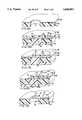
- FIGS. 13A-13EA further method of making a component incorporating the interposer, terminals and leads is shown in FIGS. 13A-13E.
- the apertures 54are formed in interposer 42, and the aperture interposer is provided with a layer 302 of adhesive on the second surface 46 of the interposer.
- a conductive sheet, such as a sheet of copper 304is applied on the first surface of the interposer, so that sheet 304 overlies adhesive 302 and so that sheet 304 overlies the apertures 54.
- a first surface 306 of sheet 304faces towards interposer 42 and confronts the second surface 46 of the interposer, with the adhesive layer 302 disposed there between.
- a second surface 308 of the conductive sheetfaces away from the interposer.
- a layer 310 of a photosensitive resist compositionis applied on the second surface 308 of conductive layer 304.
- a second resist composition 312is placed within apertures 54 so that resist 312 covers the first surface 306 of conductive layer 304 within apertures 54.
- resist 312is applied by applying a layer of the second resist composition to the first surface 44 of interposer 42 as illustrated in FIG. 13B.
- Both resist compositions 310 and 312may be provided as so-called "dry resist” i.e., as a film of resist composition which can be laminated to the other structures.
- Resist composition 312is laminated to the first surface 44 of the interposer 42 under pressure so that the resist composition flows into apertures 54 and substantially fills these apertures.
- the first resist layer 310is selectively cured and uncured portions are removed so as to leave the cured resist in a pattern corresponding to the desired pattern of conductive materials in the finished product.
- Such selective curing and removal of a resist layermay be accomplished by known photographic techniques.
- the remaining resist pattern on the second surface 308 of the conductive layer 304includes elongated lead areas 314 and terminal areas 316 contiguous with the lead areas. At least a part of each lead area 314 overlies one of the apertures 54 in the interposer, whereas the terminal areas 316 do not overly the apertures.
- each lead area 314 overlying an apertureis smaller than the aperture, so that each lead area overlies only a portion of the associated aperture 54.
- each lead area 54protrudes lengthwise across the aperture 54, as illustrated in FIG. 13C.
- the second resist material 312 within apertures 54desirably also is cured.
- the second resist materialmay be cured in its entirety, and need not be cured selectively in a predetermined pattern, the second resist material may be of a type which can be cured by exposure to heat or other nonselective curing method. Alternatively, the second resist material 312 may be photographically cured.
- the assemblyis immersed in an etchant capable of dissolving the conductive material in layer 304 so that the etchant contacts this layer.
- an etchantcapable of dissolving the conductive material in layer 304 so that the etchant contacts this layer.
- the first resist in lead area 314 and terminal areas 316protects the second surface 308 of conductive layer 304.
- the interposer 42protects the first surface 306 of layer 304 in the terminal areas 316 and in those portions of lead areas 314 which do not overly apertures 54.
- the second resist 312protects the first surface 306 in those portions of lead areas 314 which overlie apertures 54.
- the etchanttherefore does not attack those portions of conductive layer 304 covered by lead portions 314 and terminal portions 316 of the first resist layer 310.
- the first resist layer 310 and the second resist 312are then removed by conventional resist decomposition processes such as exposure to solvents which attack the resist. This leaves the unattacked portions of conductive layer 304 as leads 50 and terminals 48 on the second surface 46 of interposer 42, with a contact end 56 of each lead 50 protruding over the associated aperture 54 and with a terminal end 58 of each lead connected to the associated terminal 48.
- the adhesive layer 302may be omitted where the conductive layer forms a satisfactory bond to the material of the interposer.
- the pattern first resist 310need not be provided by a subtractive process as discussed above but instead may be provided by an additive process, wherein the resist is applied only in the areas to form the pattern, as by silkscreening. Formation of the leads 50 and terminal 48 by this type of etching process is particularly useful in forming fine leads in good registration with apertures 54. Also, as the apertures 54 are pre-formed, there is no possibility of damaging the leads during formation of the apertures.
- the interposersmay be provided in the form of a continuous tape 70, with plural interposers 42 spaced lengthwise along the tape, each such interposer having terminals 48 and leads 50 thereon.
- Tape 70may be in the form of a single sheet of the material employed for the interposers 42, or else may include separate pieces of such material, each constituting one or more interposers, secured to a backing or the like.
- Tape 70may have sprocket holes (not shown) or other features such as those commonly utilized on the tapes for tape automated bonding of semiconductor chips.
- tape 70is advanced in a downstream direction (to the right as seen in FIG. 6) and chips 28 are connected to the tape upon assembly of each chip with one interposer 42 and with the associated terminals and leads.
- the chipsare subsequently carried downstream with the tape, through further operations as discussed below.
- each interposerWith the terminals 48 and leads 50 thereon, is brought into juxtaposition with a chip 28, and the chip is aligned with the interposer so that each aperture 54 is aligned with one contact 40 of the chip.
- the interposer 42 and chip 28are brought together, so that the first face 44 of the interposer bears on the front face 38 of the chip, and the contacts are received in the apertures 54 of the interposer.
- the back end 56 of each lead 50initially lies substantially in the plane of the second surface 46 of the interposer.
- a tool 74is advanced into engagement with the contact end 56 of each lead so as to deform the contact end 56 downwardly, into the underlying aperture 54 and towards the associated contact 40.
- Tool 74may be a substantially conventional thermal bonding tool, thermosonic bonding tool, ultrasonic bonding tool, compression bonding tool, or the like of the types commonly used in tape automated bonding or wire bonding. By advancing the tool 74 into each aperture 54, the contact ends of leads are manipulated within the apertures and bonded to the contacts 40 on the chip. Although only a single tool 74 is depicted in FIG. 7, the bonding operation may be performed in a multiple operation, with many or all of the leads 50 being bonded to the associated contacts at once.
- the interposer and the chipare advanced to a further station, where the encapsulant 60 is applied within each aperture 54.
- the encapsulant 60may be applied dropwise, by conventional drop application equipment. As best seen in FIG. 8, each drop of encapsulant 60 covers the contact end 56 of the associated lead, but leaves the associated contact 48 uncovered. The encapsulant protects the relatively delicate contact ends 56 of the leads and the relatively delicate junctures with the terminals 40.
- the assembly of the interposer, leads, terminals and chipsis advanced to a testing station. As illustrated in FIG. 8, the assembly, including the chip 28, may be tested.
- the testmay involve connection of the chip, through the terminals 48, to an external electronic test device (not shown).
- the test devicemay be arranged to operate the chip under power for an appreciable period so as to "burn-in” the chip and detect any latent defects.
- numerous connectionsshould be established to the chip simultaneously. As illustrated in FIG. 8, this may be accomplished by applying probes 76 to terminals 48.
- Probes 76may be so called “noncompliant" probes. That is, probes may be arranged to move in unison, in the directions towards and away from the chip 28 (upwardly and downwardly as seen in FIG. 8).
- the probes 76are mounted to a common fixture (not shown) so that the vertical position of the probes relative to one another are fixed.
- noncompliant probe arrayis particularly convenient where the required spacings between probes (the spacings of the terminals 48) are relatively small.
- interposer 42is compliant, so that each terminal 48 can be displaced slightly by the associated probe 76 in the direction toward chip 28. The region of interposer 42 beneath each terminal 48 compresses slightly to accommodate such displacement. This allows all of the probes 76 to engage their associated contacts 48 without imposing excessive loading on any one probe.
- the terminals 48may be larger than the contacts on the chip, so as to provide a relatively large area for engagement by each contact 76 and thus accommodate a reasonable amount of misalignment of the contacts in the directions parallel to the faces of the interposer. Because each chip can be tested in this fashion, prior to assembly with the substrate, defects in the chips, in the terminals and leads associated with the interposer and in the bonds between the leads and the chip contacts can be detected before the chip is united with the substrate.
- the chip and interposerare united with the substrate.
- the chip and interposer assemblyis oriented so that the second face of the interposer, and the terminals 48, face the top surface of the substrate, and each terminal 48 confronts one contact pad 24 on substrate.
- Masses of solderare applied between the confronting terminals 48 and contact pads 24 and melted in a "solder reflow" operation so that the solder forms a solid joint between the contact pad and terminal, and so that the solder masses support the chip and interposer assembly above the substrate 20, in the orientation illustrated in FIG. 2.
- the solder application and reflow operationmay be performed in substantially the same way as the solder application and reflow operation of conventional flip-chip bonding.
- the masses of soldermay initially be applied to the contact pads 24 of the substrate, before the chip and interposer assembly is united with the substrate.
- the soldermay be applied to the terminals 48 and bonded to the contact pads 24 in the reflow operation.
- a fluxtypically is employed in the solder reflow operation. Because the solder masses support the chip and interposer surface assembly above the substrate, there is a gap 80 between the interposer and the substrate. Flux residues may be rinsed out of the assembly by passing a rinsing fluid through this gap.
- the interposer 42is not provided with leads before the interposer is united with the chip 28. Instead, leads 50' are applied by bonding separately formed pieces of fine wire to the terminals 48 and to the contacts 40 after the interposer is assembled with the chip. Leads 50' are flexible and curved, and arranged to deform as discussed above so that each contact 40, and the associated contact end of the lead 50' can move relative to the associated terminal 48 so as to accommodate thermal expansion.
- a layer of an adhesive 81is disposed between the first surface of the interposer and the front surface of the chip.
- the subassembly illustrated in FIG. 9is further provided with an encapsulant 60' (FIG. 10) in the form of a layer covering substantially the entire second face 46 of interposer 42 and hence filling the apertures 54 and covering the leads 50'.
- the layer 60'is provided with holes 82 in alignment with the terminals 48. Holes 82 may be formed by etching layer 60, by applying layer 60' in a selective coating process such as silk screening or the like or by applying layer 60' in a selective curing process.
- layer 60'may be formed by an encapsulant which is curable by ultraviolet or other radiant energy.
- the encapsulantmay be deposited over the entire interposer, and over terminals 48.
- radiant energymay be applied selectively, so that the areas of the layer overlying terminals 48 remain uncured. These layers are then removed by washing or by a relatively mild etching operation, leaving the holes 82 in alignment with terminals 48. Masses of electrically conductive bonding material 52' are deposited within holes 82 in the encapsulant layer. These masses are then engaged with the contact pads (not shown) of the substrate and heated so that bonding material 52' forms a bond between each terminal 48 and the associated contact pad on the substrate, in a manner similar to the solder bonds of the assembly depicted in FIG. 2.
- a chip 128may have contacts 140 disposed in a peripheral arrangement, i.e., where all of the contacts 140 are disposed adjacent the periphery of the chip.
- the central zone of the contact pattern area, adjacent the geometric center 164 of the contact array,is devoid of contacts.
- the terminals 148 on the interposermay be arranged in a "fan in" pattern, i.e., where the mean distance from the geometric center 164 to the terminals 148 is less than the mean distance from the geometric center to the contacts 140.
- Some of the terminals 148are disposed on the area of the interposer overlying the central zone of the contact pattern area, i.e., adjacent center 164.
- This arrangementcan provide a substantially uniform distribution of terminals over an area equal to the contact pattern area, i.e., over the area encompassed by contacts 140. This provides a spacing between adjacent terminals larger than the spacing between adjacent contacts 140. This allows connection of chips with peripheral contact arrays to area arrays of contact pads on the substrate. Thus chips originally intended for conventional bonding processes such as tape automated bonding can be adapted readily and economically to substrates having compact contact pad arrays similar to those used in flip-chip bonding.
- the structure illustrated in FIG. 12has an interposer 242 with terminals 248 and leads 250 substantially as discussed above with reference to FIGS. 1-4.
- leads 250are curved in directions parallel to the face 246 of the interposer 242 and parallel to the plane of the front face 238 of chip 228. This provides increased flexibility in lead 250.
- the curved portion of each leadoverlies the aperture 254.
- the curved portion of the leadis not bonded to the interposer 242. This portion of the lead therefore can flex to accommodate movement of contact 240 relative to terminal 248 without deformation of the interposer 242.
- Contacts 248however, which are formed integrally with the leads 250 are bonded to the surface of interposer 242.
- chips 428may be provided in the form of a wafer incorporating a plurality of chips, all of the same design or of differing designs.
- Individual interposers 442may be positioned on the individual chips 428 constituting wafer 430, and the interposers may be assembled to the chips as discussed above.
- the contacts on each chip 428are secured to the leads and terminals of each interposer.
- the individual chipsare separated from the wafer and from one another, as by cutting the wafer using conventional wafer severing or "dicing" equipment commonly utilized to sever individual chips without interposers. This procedure yields a plurality of chip and interposer subassemblies, each of which may be secured to an individual substrate.
- a wafer 530 incorporating a plurality of chipsmay be assembled to a sheet 535 incorporating a plurality of interposers 542. Again, the contacts on each chip are secured to the terminals and leads of one individual interposer overlying the particular chip.
- the wafer 530 and the sheet 535are severed after this operation, and desirably after encapsulating the leads, so as to provide individual subassemblies each including a chip and an interposer.
- Interposeralso may be provided in the form of a sheet 635 incorporating plural interposers such as interposer 642 and 643 at predetermined relative positions corresponding to the positions of chips on a completed assembly including a substrate. Chips such as chips 628 and 629 may be secured to the individual interposers and the entire assembly of plural chips and the sheet of plural interposers may be secured to a substrate 620. Each interposer in such an assembly desirably incorporates a pattern of terminals and leads as discussed above. This variant of the assembly procedures provides for consolidation of plural chips into a larger subassembly before bonding to the substrate.
- the semiconductor chipmay be formed from a material selected from the group consisting of silicon based and gallium arsenide based semiconductor materials, or from other suitable compositions.
- semiconductor chipis used herein in this disclosure in the conventional sense, as referring to a chip having portions which are semiconductive so as to accomplish the required electronic functions.
- substrate materialsmay be employed.
- the substratemay be formed from ceramic, polymeric and metallic structural materials, and from composites including these materials.
- the interposeritself may be formed from a wide variety of materials.
- Flexible interposerstypically are fabricated from polymeric materials such as polyimides and other thermosetting polymers, fluoro polymers and thermoplastic polymers.
- the interposermay be a composite incorporating plural materials.
- the interposermay consist of, or incorporate, a foam or mesh layer.
- the flexibility of the interposerdepends on the thickness and configuration of the interposer, as well as on the properties of the materials used therein.
- a flexible interposercapable of buckling or wrinkling to accommodate relative movement, can be fabricated from high elastic modulus materials, normally considered as "rigid" provided that these materials are present in thin layers.
- Relatively soft materials and foamscan be used in greater thicknesses and still provide a highly flexible interposer. Moreover, such soft materials and foams provide a highly compliant interposer, i.e., an interposer which is readily compressible in the directions perpendicular its surfaces and which therefore permits movement of the terminals in these directions. As discussed above with reference to FIG. 8, such compliance facilitates testing operations.
- the leads and terminalscan be fabricated from conventional materials of types commonly employed for semiconductor chip leads. Metals, including copper, noble metals such as gold and silver, or copper based alloy with noble metal overcoating can be employed.
- the terminalscan also be formed from composite materials including conductive epoxies, metal filled polymers or intrinsically conducting polymeric compositions such as polyacetylene.
- the terminalscan also be formed from alloys commonly regarded as soldering or brazing alloys such as lead-tin, gold-tin or silver-copper alloys.
- the encapsulantdesirably is a soft material having a very low elastic modulus.
- the encapsulantmay have properties similar to those of rubber, gum or gel.
- the leadsand desirably the interposer itself, are flexible so as to permit movement of the contact ends of the leads relative to the terminals without imposing substantial forces on the juncture between the contact ends of the leads and the contacts on the chip, or on the bonding material securing the terminals to the contact pads of the substrate.
- the minimum degree of flexibility required in a given applicationvary with the properties of the materials employed and with the temperatures expected in service. Desirably, however the forces required to bend or deform the leads will not cause early thermal cycling damage of the joints between the contact ends of the leads and the chip contacts, or the fatigue limits of the bonding materials.
- a conservative design approachis to assume the maximum temperature changes to be encountered in service and the maximum temperature differentials between components (such as between the chip and substrate) expected in service with a safety margins as commonly employed in the semi-conductor industry. Based upon these assumptions, the maximum possible relative movement between any chip contact and any contact pad on the substrate can be calculated according to commonly used finite element analysis methods. The stress for leads of various flexibilities can then be compared to known data for maximum thermal stress on metallurgical bonds of a particular type, and the appropriate design may be selected. Preferably, however, leads of various flexibilities are fabricated and tested.
Landscapes
- Engineering & Computer Science (AREA)
- Microelectronics & Electronic Packaging (AREA)
- Computer Hardware Design (AREA)
- Power Engineering (AREA)
- Physics & Mathematics (AREA)
- Condensed Matter Physics & Semiconductors (AREA)
- General Physics & Mathematics (AREA)
- Manufacturing & Machinery (AREA)
- Wire Bonding (AREA)
Abstract
Description
This is a continuation of application Ser. No. 08/278,394, filed on Jul. 21, 1994, now abandoned, which is a Divisional of Ser. No. 07/865,984, filed on Apr. 9, 1992, which issued as U.S. Pat. No. 5,346,861 on Sep. 13, 1994, which is a Divisional of Ser. No. 07/586,758 filed on Sep. 24, 1990, which issued as U.S. Pat. No. 5,148,266 on Sep. 15, 1992.
The present invention relates to the art of electronic packaging, and more specifically to assemblies incorporating semiconductor chips and to methods of making such assemblies.
Modern electronic devices utilize semiconductor chips, commonly referred to as "integrated circuits" which incorporate numerous electronic elements. These chips are mounted on substrates which physically support the chips and electrically interconnect each chip with other elements, of the circuit. The substrate may be a part of a discrete chip package used to hold a single chip and equipped with terminals for interconnection to external circuit elements. Such substrates may be secured to an external circuit board or chassis. Alternatively, in a so-called "hybrid circuit" one or more chips are mounted directly to a substrate forming a circuit panel arranged to interconnect the chips and the other circuit elements mounted to the substrate. In either case, the chip must be securely held on the substrate and must be provided with reliable electrical interconnection to the substrate. The interconnection between the chip itself and its supporting substrate is commonly referred to as "first level" assembly or chip interconnection, as distinguished from the interconnection between the substrate and the larger elements of the circuit, commonly referred to as a "second level" interconnection.
The structures utilized to provide the first level connection between the chip and the substrate must accommodate all of the required electrical interconnections to the chip. The number of connections to external circuit elements, commonly referred to as "input-output" or "I/O" connections, is determined by the structure and function of the chip. Advanced chips capable of performing numerous functions may require hundreds or even thousands of I/O connections to a single chip.
The size of the chip and substrate assembly is a major concern. The size of each such assembly influences the size of the overall electronic device. Moreover, the size of each assembly controls the required distance between each chip and other chips, or between each chip or other elements of the circuit. Delays in transmission of electrical signals between chips are directly related to these distances. These delays limit the speed of operation of the device. For example, in a computer where a central processing unit operates cyclically, signals must be interchanged between the central processing unit chip and other chips during each cycle. The transmission delays inherent in such interchanges often limit the clock rate of the central processing chip. Thus, more compact interconnection assemblies, with smaller distances between chips and smaller signal transmission delays can permit faster operation of the central processing chip.
The first level interconnection structures connecting a chip to a substrate ordinarily are subject to substantial stress caused by thermal cycling as temperatures within the device change during operation. The electrical power dissipated within the chip tends to heat the chip and substrate, so that the temperature of the chip and substrate rises each time the device is turned on and falls each time the device is turned off. As the chip and the substrate ordinarily are formed from different materials having different coefficients of thermal expansion, the chip and substrate ordinarily expand and contract by different amounts. This causes the electrical contacts on the chip to move relative to the electrical contact pads on the substrate as the temperature of the chip and substrate changes. This relative movement deforms the electrical interconnections between the chip and substrate and places them under mechanical stress. These stresses are applied repeatedly with repeated operation of the device, and can cause breakage of the electrical interconnections. Thermal cycling stresses may occur even where the chip and substrate are formed from like materials having similar coefficients of thermal expansion, because the temperature of the chip may increase more rapidly than the temperature of the substrate when power is first applied to the chip.
The cost of the chip and substrate assembly is also a major concern. All these concerns, taken together, present a formidable engineering challenge. Various attempts have been made heretofore to provide primary interconnection structures and methods to meet these concerns, but none of these is truly satisfactory in every respect. At present, the most widely utilized primary interconnection methods are wire bonding, tape automated bonding or "TAB" and flip-chip bonding.
In wire bonding, the substrate has a top surface with a plurality of electrically conductive contact pads or lands disposed in a ring-like pattern, The chip is secured to the top surface of the substrate at the center of the ring-like pattern, so that the chip is surrounded by the contact pads on the substrate. The chip is mounted in a face-up disposition, with the back surface of the chip confronting the top surface of the substrate and with the front surface of the chip facing upwardly, away from the substrate, so that electrical contacts on the front surface are exposed. Fine wires are connected between the contacts on the front face of the chip and the contact pads on the top surface of the substrate. These wires extend outwardly from the chip to the surrounding contact pads on the substrate.
Wire bonding ordinarily can only be employed with contacts at the periphery of the chip. It is difficult or impossible to make connections with contacts at the center of the front surface of the chip using the wire bonding approach. Also, the contacts on the chip must be spaced at least about 100 micrometers apart from one another. These considerations limit the wire bonding approach to chips having relatively few I/O connections, typically less than about 250 connections per chip. Moreover, the area of the substrate occupied by the chip, the wires and the contact pads of the substrate is substantially greater than the surface area of the chip itself.
In tape automated bonding, a polymer tape is provided with thin layers of metallic material forming conductors on a first surface of the tape. These conductors are arranged generally in a ring-like pattern and extend generally radially, towards and away from the center of the ring-like pattern. The chip is placed on the tape in a face down arrangement, with contacts on the front surface of the chip confronting the conductors on the first surface of the tape. The contacts on the chip are bonded to the conductors on the tape. Ordinarily, numerous patterns of conductors are arranged along the length of the tape and one chip is bonded to each of these individual patterns, so that the chips, once bonded to the tape, can be advanced through successive work stations by advancing the tape. After each chip is bonded to the metallic conductors constituting one pattern, the chip and the immediately adjacent portions of the pattern are encapsulated and the outermost portions of the metallic conductors are secured to additional leads and to the ultimate substrate. Tape automated bonding can provide the assembly with good resistance to thermal stresses, because the thin metallic leads on the tape surface are quite flexible, and will bend readily upon expansion of the chip without imposing significant stresses at the juncture between the lead and the contact on the chip. However, because the leads utilized in tape automated bonding extend outwardly in a radial, "fan out" pattern from the chip, the assembly necessarily is much larger than the chip itself. Also, the leads ordinarily are connected only to contacts at the periphery of the chip. This limits tape automated bonding to chips having relatively low numbers of contacts.
In flip-chip bonding, contacts on the front surface of the chip are provided with bumps of solder. The substrate has contact pads arranged in an array corresponding to the array of contacts on the chip. The chip, with the solder bumps, is inverted so that its front surface faces toward the top surface of the substrate, with each contact and solder bump on the chip being positioned on the appropriate contact pad of the substrate. The assembly is then heated so as to liquify the solder and bond each contact on the chip to the confronting contact pad of the substrate. Because the flip-chip arrangement does not require leads arranged in a fan-out pattern, it provides a compact assembly. The area of the substrate occupied by the contact pads is approximately the same size as the chip itself. Moreover, the flip-chip bonding approach is not limited to contacts on the periphery of the chip. Rather, the contacts on the chip may be arranged in a so-called "area array" covering substantially the entire front face of the chip. Flip-chip bonding therefore is well suited to use with chips having large numbers of I/O contacts. However, assemblies made by flip-chip bonding are quite susceptible to thermal stresses. The solder interconnections are relatively inflexible, and may be subjected to very high stress upon differential expansion of the chip and substrate. These difficulties are particularly pronounced with relatively large chips. Moreover, it is difficult to test and operate or "burn-in" chips having an area array of contacts before attaching the chip to the substrate.
Thus, despite all of the effort which has been devoted to development of semiconductor chip assemblies and assembly methods heretofore, there are considerable unmet needs for further improvements.
The present invention addresses these needs.
One aspect of the present invention provides a semiconductor chip assembly. A chip assembly according to this aspect of the invention includes a semiconductor chip having a front surface with a plurality of contacts disposed in a pattern on the front surface. The pattern of contacts on the front surface encompasses an area, referred to herein as the "contact pattern area" on the front surface. The chip assembly according to this aspect of the invention also includes a sheetlike dielectric interposer overlying the front surface of the chip. The interposer has a first surface facing toward the chip and a second surface facing away from the chip. An area of the interposer overlies the contact pattern area of the chip. The interposer has apertures extending through it, from the first surface to the second surface. The interposer also has a plurality of electrically conductive terminals disposed in a pattern on the second surface of the interposer. At least some of these terminals, and preferably most or all of these terminals, are disposed within the area of the interposer overlying the contact pattern area on the chip. Each such terminal is associated with one contact on the chip.
The assembly also includes flexible, electrically conductive leads. The leads preferably extend through the apertures in the interposer. Each such lead has a contact end connected to the associated contact of the chip and a terminal end connected to the associated terminal on the second surface of the interposer. The leads and the interposer are constructed and arranged so that the contact ends of the leads are moveable relative to the terminals at least to the extent required to compensate for differential thermal expansion of components. The leads desirably are flexible to permit such movement. Most preferably, the interposer itself is flexible so as to facilitate such movement.
The assembly incorporating the chip, interposer, terminals and leads may be incorporated in a larger assembly including a substrate having a top surface facing toward the second surface of the interposer. A plurality of connection pads preferably are disposed on the top surface of the substrate in an array corresponding to the array of terminals on the second surface of the interposer, so that the pads confront the terminals. Means for bonding the pads on the substrate to the terminals on the interposer may be provided. These means may include masses of solder or other electrically conductive material.
Preferred chip assemblies according to this aspect of the present invention are compact and may be utilized with chips having large numbers of input-output connections. The terminals on the interposer, and the corresponding contact pads on the substrate, desirably are disposed in areas substantially the same size as the contact pattern area on the chip itself. Moreover, the contacts on the chip may be arranged in any pattern, and need not be limited to the periphery of the chip. For example, the contacts on the chip can be distributed evenly over the chip face in a so called "area array". Because the contact end of each lead is moveable with respect to the terminal associated with that lead, stresses caused by thermal cycling are markedly reduced. Movement of the contacts on the chip relative to the contact pads on the substrate, such as that caused by expansion of the chip, is taken up by flexing of the leads and movement of the contact ends of the leads relative to the terminals. The ability to take up substantial relative movement of the chip contacts and substrate contact pads without inducing substantial stresses in the electrical connections allows for use of substrate and chip materials having widely differing coefficients of thermal expansion. Assemblies according to this aspect of the present invention thus provide a unique combination of advantages heretofore unattainable in a single structure.
The flexible leads may be formed integrally with the terminals on the interposer, or else may be separately formed fine wires. The leads desirably are curved to provide increased flexibility. The interposer desirably is a thin, flexible sheet of a polymeric material such as polymide, a fluoropolymer, a thermoplastic polymer or an elastomer. In this arrangement, flexing of the interposer facilitates movement of the contact ends of the leads relative to the terminals and thus contributes to the ability of the assembly to withstand thermal cycling. The assembly may also include a compliant dielectric encapsulant having a low elastic modulus, such as an elastomeric encapsulant, covering the flexible leads in whole or in part. The encapsulant may be provided in the form of a layer, with holes in the encapsulant layer aligned with the terminals on the second surface of the interposer. The bonds between the terminals and the contact pads of the substrate extend through these holes. The encapsulant protects the relatively delicate leads during handling and during service, but does not materially impair the flexibility of the leads or the ability of the leads to take up relative motion of the chip and substrate during thermal expansion.
A further aspect of the present invention provides methods of assembling semiconductor chips to substrates. A method according to this aspect of the present invention preferably includes the steps of assembling a sheet-like dielectric interposer having first and second surfaces to a chip so that a first surface of the interposer confronts the front surface of the chip and a portion of the interposer overlies the contact pattern area encompassed by a pattern of contacts on the front surface of the chip. The method also includes the step of connecting the contacts on the chip to terminals disposed on the second surface of the interposer, facing away from the chip, at least some of the terminals overlying the contact pattern area of the chip. The connecting step preferably is performed by connecting flexible leads so that leads extend between the contacts on the chip and the terminals on the interposer through apertures in the interposer, and so that each such terminal is moveable with respect to the contact connected therewith. The method preferably also includes the steps of assembling a substrate with the assembled interposer and chips so that contact pads on a top surface of the substrate confront the terminals on the interposer, and bonding the terminals to the pads. Preferably, the interposer has the terminals positioned thereon prior to assembly of the interposer to the chip before the interposer is assembled with the chip. The leads may be connected to the contacts on the chip by manipulating the leads through the apertures in the interposer. The terminals on the interposer may be bonded to the contact pads of the substrate by application of a fusible material, such as bumps of solder.
The method most preferably includes the step of testing the assembled chip, interposer, leads and terminals prior to assembly of the substrate with these components. The testing procedure may include operation of the chip for a period sufficient to detect latent defects, commonly referred to as "burn in". The interposer and terminals greatly facilitate the testing process. Temporary connections may be made to the terminals, as by applying electrically conductive probes to the terminals, during the testing procedure. The terminals provide substantial areas for engagement by such probes. Most desirably, the substrate is compliant, so that the terminals can be displaced slightly by the probes. This greatly facilitates engagement of the terminals with multiple or "ganged", probes and particularly with non-compliant probes and thus facilitates the testing operation. The assembly method according to this aspect of the present invention may also include the step of applying an encapsulant to cover at least parts of the flexible leads. Desirably, the encapsulant is applied before assembly of the substrate and before the testing step. The interposer may serve as a carrier for the chip during the test, encapsulation and substrate assembly operations. The preferred processes according to this aspect of the present invention thus provide economical assembly methods.
Still further aspects of the invention provide prefabricated components including an interposer, terminals and leads, and methods of making such components.
These and other objects, features and advantages of the present invention will be more readily apparent from the detailed description of the preferred embodiment set forth below taken in conjunction with the accompanying drawings.
FIG. 1 is a diagrammatic perspective view of a chip assembly in accordance with one embodiment of the invention.
FIG. 2 is a fragmentary sectional view taken alongline 2--2 in FIG. 1.
FIG. 3 is a fragmentary view, on an enlarged scale, of the area indicated in FIG. 2.
FIG. 4 is a layout diagram depicting the spatial relationship of certain components in the assembly of FIG. 1.
FIGS. 5A and 5B are fragmentary diagrammatic perspective views depicting certain operations, in manufacture of a component utilized in the assembly of FIG. 1.
Each of FIGS. 6, 7 and 8 is a fragmentary diagrammatic perspective view depicting certain operations in the process of manufacture of the assembly of FIG. 1.
FIG. 9 is a fragmentary diagrammatic perspective view similar to FIG. 7 but depicting components and process steps in accordance with a further embodiment of the invention.
FIG. 10 is a fragmentary sectional view depicting the components of FIG. 9 during a further step in the process.
FIG. 11 is a layout diagram similar to FIG. 4 but depicting an assembly in accordance with a further embodiment of the invention.
FIG. 12 is a fragmentary diagrammatic perspective view depicting a portion of an assembly in accordance with a further embodiment of the invention.
Each of FIGS. 13A through 13E is a fragmentary diagrammatic perspective view depicting a stage in a further component fabrication process according to the invention.
Each of FIGS. 14, 15 and 16 is a diagrammatic perspective view depicting further processes according to the invention.
Each chip assembly in accordance with one embodiment of the present invention includes arigid substrate 20 having atop surface 22 and havingcontact pads 24 disposed on the top surface.Substrate 20 is also provided withconductors 26 interconnecting certain ones of thecontact pads 24. Thecontact pads 24 are arranged in a pattern on the top surface of the substrate generally corresponding to the pattern of connections to devices, such assemiconductor chips discrete components 32 mounted on the substrate.Substrate 20 also has external connections such as pins 34. Theconductors 26 are arranged to interconnect thevarious contact pads 24 in the desired patterns so as to interconnectchips discrete components 32 and to theexternal connectors 34 in the appropriate manner for functioning of the particular circuit. Although only afew contact pads 24,conductors 26 andexternal connections 34 are illustrated in FIG. 1, thesubstrate 20 may have an unlimited number ofcontact pads 24,conductors 26 andexternal connections 34. Hundreds or thousands of these elements typically are provided in each substrate.
Thecontact end 56 of each lead 50 is moveable relative to the associatedterminal 48. As best seen in FIG. 3, the contact end 56a oflead 50a can be displaced from its normal, undeformed position (shown in solid lines) in the directions parallel to thefaces interposer 42 and parallel to thefront face 38 ofchip 28. Displacement in one such direction is indicated by the arrows in FIGS. 2 and 3. For example, the contact end 56a may be displaced to the position indicated in broken lines at 56a'. This displacement is permitted by the flexibility of thelead 50 and by buckling and wrinkling ofinterposer 42.Encapsulant 60 is compliant, and does not substantially resist flexing ofleads 50 and buckling and wrinkling ofinterposer 42. The displacement illustrated in FIG. 3, from the normal undisplaced position 56a to the displaced position 56a' places thelead 50 in compression. That is, the terminal end 56a moves generally toward the associated terminal 48 in moving from position 56a to position 56a'. Movement in this direction is particularly well accommodated by buckling of thelead 50. The contact end of each lead can also move in other directions, such as in the opposite direction from position 56a away from the associatedterminal 48, and in directions perpendicular to these directions, into and out of the plane of the drawing as seen in FIG. 3.
As best seen in FIG. 4, thecontacts 40 on chip 28 (each symbolized by a dot in FIG. 4) are disposed in a pattern on the front surface ofchip 28.Contacts 40 cooperatively encompass a contact pattern area 62 on the front face ofchip 28. The boundary of the contact pattern area is illustrated by a broken line B in FIG. 4. The boundary of the contact pattern area may be taken as the shortest combination of imaginary line segments along the front face of the chip which cooperatively enclose all of thecontacts 40. In the particular example illustrated in FIG. 4, this boundary is generally in the form of a rectangle.Contacts 40 are disposed throughout contact pattern area 62, in locations determined by the interior structure ofchip 28. Contact pattern area 62 includes a peripheral region, adjacent the boundary B, and a central region, adjacent thegeometric center 64 of the contact pattern area.Contacts 40 are disposed both in the peripheral region and in the central region. Typically, although not necessarily, thecontacts 40 are disposed at substantially equal spacings throughout the entirety of contact pattern area 62. Theterminals 48, each symbolized by a X in FIG. 4, are disposed in a similar pattern on thesecond surface 46 ofinterposer 42. At least some ofterminals 48 are disposed in the area ofinterposer surface 46 overlying contact pattern area 62.Terminals 48 encompass aterminal pattern area 66 on thesecond face 46 of the interposer. The boundary ofterminal pattern area 66 is illustrated in FIG. 4 by the broken line T. The boundary of the terminal pattern area may be taken as the shortest combination of imaginary line segments which would cooperatively enclose all of the terminals on the second surface of the interposer. The geometric center ofterminal array area 66 desirably is coincident, or approximately coincident, with thegeometric center 64 of the contact array area. Desirably,terminal pattern area 66 is not substantially larger than contact pattern area 62. That is, the perimeter of the terminal area preferably is less than about 1.2 times, and most preferably about 1.0 times the perimeter of contact pattern area 62. Stated another way, theoutermost terminals 48 desirably lie within or close to the boundary B of contact array area 62. The total area encompassed withinterminal pattern area 66 desirably is less than about 1.4 times, and most desirably about 1.0 times the total area encompassed within contact pattern area 62. Thus theleads 50 connectingcontacts 40 toterminals 48 do not "fan out", away from thegeometric center 64 the contact pattern area. Typically, the mean distance of theterminals 48 fromgeometric center 64 of the contact pattern area, measured in the direction parallel to the surfaces of the chip and interposer, is less than about 1.1, and typically about 1.0, times the mean distance of thechip contacts 40 fromcenter 64.
The interposer and leads utilized in the structure of FIGS. 1-4 may be fabricated by a process as schematically illustrated in FIGS. 5A-5B. In this procedure, theterminals 48 and leads 50 may be deposited on thesecond surface 46 of the sheetlike interposer by conventional printed circuit manufacturing techniques before formation ofapertures 54. Thus, the leads and terminals may be formed either by an additive process, wherein the metal is deposited in the desired pattern by plating, or else in a subtractive process which begins with a laminate including both thesheetlike interposer 42 and a full layer of metal and removes the metal except in the areas where the terminals and leads are desired, so as to yield a sheet having the terminals and leads in position (FIG. 5A). After formation of the terminals and leads,apertures 54 are formed in registration with the contact ends 56 of the leads 50 (FIG. 5B) by etching through the interposer from thefirst surface 44, or by applying radiant energy such as laser beam focused at the appropriate spots on thefirst surface 44.
A further method of making a component incorporating the interposer, terminals and leads is shown in FIGS. 13A-13E. In this method, theapertures 54 are formed ininterposer 42, and the aperture interposer is provided with alayer 302 of adhesive on thesecond surface 46 of the interposer. A conductive sheet, such as a sheet ofcopper 304 is applied on the first surface of the interposer, so thatsheet 304 overlies adhesive 302 and so thatsheet 304 overlies theapertures 54. Afirst surface 306 ofsheet 304 faces towardsinterposer 42 and confronts thesecond surface 46 of the interposer, with theadhesive layer 302 disposed there between. Asecond surface 308 of the conductive sheet faces away from the interposer. Alayer 310 of a photosensitive resist composition is applied on thesecond surface 308 ofconductive layer 304. A second resistcomposition 312 is placed withinapertures 54 so that resist 312 covers thefirst surface 306 ofconductive layer 304 withinapertures 54. Desirably, resist 312 is applied by applying a layer of the second resist composition to thefirst surface 44 ofinterposer 42 as illustrated in FIG. 13B. Both resistcompositions composition 312 is laminated to thefirst surface 44 of theinterposer 42 under pressure so that the resist composition flows intoapertures 54 and substantially fills these apertures.
In the next stage of the process, depicted in FIG. 13C, the first resistlayer 310 is selectively cured and uncured portions are removed so as to leave the cured resist in a pattern corresponding to the desired pattern of conductive materials in the finished product. Such selective curing and removal of a resist layer may be accomplished by known photographic techniques. The remaining resist pattern on thesecond surface 308 of theconductive layer 304 includeselongated lead areas 314 andterminal areas 316 contiguous with the lead areas. At least a part of eachlead area 314 overlies one of theapertures 54 in the interposer, whereas theterminal areas 316 do not overly the apertures. The portion of eachlead area 314 overlying an aperture is smaller than the aperture, so that each lead area overlies only a portion of the associatedaperture 54. Desirably, eachlead area 54 protrudes lengthwise across theaperture 54, as illustrated in FIG. 13C. The second resistmaterial 312 withinapertures 54 desirably also is cured. As the second resist material may be cured in its entirety, and need not be cured selectively in a predetermined pattern, the second resist material may be of a type which can be cured by exposure to heat or other nonselective curing method. Alternatively, the second resistmaterial 312 may be photographically cured.
In the next stage of the process, illustrated in FIG. 13D, the assembly is immersed in an etchant capable of dissolving the conductive material inlayer 304 so that the etchant contacts this layer. During the etching procedure, the first resist inlead area 314 andterminal areas 316 protects thesecond surface 308 ofconductive layer 304. Theinterposer 42 protects thefirst surface 306 oflayer 304 in theterminal areas 316 and in those portions oflead areas 314 which do not overly apertures 54. The second resist 312 protects thefirst surface 306 in those portions oflead areas 314 which overlieapertures 54. The etchant therefore does not attack those portions ofconductive layer 304 covered bylead portions 314 andterminal portions 316 of the first resistlayer 310. The first resistlayer 310 and the second resist 312 are then removed by conventional resist decomposition processes such as exposure to solvents which attack the resist. This leaves the unattacked portions ofconductive layer 304 as leads 50 andterminals 48 on thesecond surface 46 ofinterposer 42, with acontact end 56 of each lead 50 protruding over the associatedaperture 54 and with aterminal end 58 of each lead connected to the associatedterminal 48.
This process can be modified. For example, theadhesive layer 302 may be omitted where the conductive layer forms a satisfactory bond to the material of the interposer. Also, the pattern first resist 310 need not be provided by a subtractive process as discussed above but instead may be provided by an additive process, wherein the resist is applied only in the areas to form the pattern, as by silkscreening. Formation of theleads 50 and terminal 48 by this type of etching process is particularly useful in forming fine leads in good registration withapertures 54. Also, as theapertures 54 are pre-formed, there is no possibility of damaging the leads during formation of the apertures.
The assembly of the interposer and terminals and contacts is fabricated in a substantially continuous sheet or strip. As illustrated in FIG. 6, the interposers may be provided in the form of acontinuous tape 70, withplural interposers 42 spaced lengthwise along the tape, each suchinterposer having terminals 48 and leads 50 thereon.Tape 70 may be in the form of a single sheet of the material employed for theinterposers 42, or else may include separate pieces of such material, each constituting one or more interposers, secured to a backing or the like.Tape 70 may have sprocket holes (not shown) or other features such as those commonly utilized on the tapes for tape automated bonding of semiconductor chips.
In an assembly method according to the invention,tape 70 is advanced in a downstream direction (to the right as seen in FIG. 6) andchips 28 are connected to the tape upon assembly of each chip with oneinterposer 42 and with the associated terminals and leads. The chips are subsequently carried downstream with the tape, through further operations as discussed below.
As best seen in FIG. 7, each interposer, with theterminals 48 and leads 50 thereon, is brought into juxtaposition with achip 28, and the chip is aligned with the interposer so that eachaperture 54 is aligned with onecontact 40 of the chip. Theinterposer 42 andchip 28 are brought together, so that thefirst face 44 of the interposer bears on thefront face 38 of the chip, and the contacts are received in theapertures 54 of the interposer. Theback end 56 of each lead 50 initially lies substantially in the plane of thesecond surface 46 of the interposer. Atool 74 is advanced into engagement with thecontact end 56 of each lead so as to deform thecontact end 56 downwardly, into the underlyingaperture 54 and towards the associatedcontact 40.Tool 74 may be a substantially conventional thermal bonding tool, thermosonic bonding tool, ultrasonic bonding tool, compression bonding tool, or the like of the types commonly used in tape automated bonding or wire bonding. By advancing thetool 74 into eachaperture 54, the contact ends of leads are manipulated within the apertures and bonded to thecontacts 40 on the chip. Although only asingle tool 74 is depicted in FIG. 7, the bonding operation may be performed in a multiple operation, with many or all of theleads 50 being bonded to the associated contacts at once.
After the contacts and leads have been bonded to one another, the interposer and the chip are advanced to a further station, where theencapsulant 60 is applied within eachaperture 54. Theencapsulant 60 may be applied dropwise, by conventional drop application equipment. As best seen in FIG. 8, each drop ofencapsulant 60 covers thecontact end 56 of the associated lead, but leaves the associatedcontact 48 uncovered. The encapsulant protects the relatively delicate contact ends 56 of the leads and the relatively delicate junctures with theterminals 40. Once the encapsulant has been applied, the assembly of the interposer, leads, terminals and chips is advanced to a testing station. As illustrated in FIG. 8, the assembly, including thechip 28, may be tested. The test may involve connection of the chip, through theterminals 48, to an external electronic test device (not shown). The test device may be arranged to operate the chip under power for an appreciable period so as to "burn-in" the chip and detect any latent defects. Typically, numerous connections should be established to the chip simultaneously. As illustrated in FIG. 8, this may be accomplished by applyingprobes 76 toterminals 48.Probes 76 may be so called "noncompliant" probes. That is, probes may be arranged to move in unison, in the directions towards and away from the chip 28 (upwardly and downwardly as seen in FIG. 8). Theprobes 76 are mounted to a common fixture (not shown) so that the vertical position of the probes relative to one another are fixed. This type of "noncompliant" probe array is particularly convenient where the required spacings between probes (the spacings of the terminals 48) are relatively small. However, non-uniformities in the dimensions of theprobes 76 and/or in the dimensions of theterminals 48 orchip 28 may cause one or more of theprobes 76 to engage the associatedterminal 48 before the other probes have engaged their terminals. Desirably,interposer 42 is compliant, so that each terminal 48 can be displaced slightly by the associatedprobe 76 in the direction towardchip 28. The region ofinterposer 42 beneath each terminal 48 compresses slightly to accommodate such displacement. This allows all of theprobes 76 to engage their associatedcontacts 48 without imposing excessive loading on any one probe. Theterminals 48 may be larger than the contacts on the chip, so as to provide a relatively large area for engagement by eachcontact 76 and thus accommodate a reasonable amount of misalignment of the contacts in the directions parallel to the faces of the interposer. Because each chip can be tested in this fashion, prior to assembly with the substrate, defects in the chips, in the terminals and leads associated with the interposer and in the bonds between the leads and the chip contacts can be detected before the chip is united with the substrate.
After the testing operation, the chip and interposer are united with the substrate. The chip and interposer assembly is oriented so that the second face of the interposer, and theterminals 48, face the top surface of the substrate, and each terminal 48 confronts onecontact pad 24 on substrate. Masses of solder are applied between the confrontingterminals 48 andcontact pads 24 and melted in a "solder reflow" operation so that the solder forms a solid joint between the contact pad and terminal, and so that the solder masses support the chip and interposer assembly above thesubstrate 20, in the orientation illustrated in FIG. 2. The solder application and reflow operation may be performed in substantially the same way as the solder application and reflow operation of conventional flip-chip bonding. Thus, the masses of solder may initially be applied to thecontact pads 24 of the substrate, before the chip and interposer assembly is united with the substrate. Alternatively, the solder may be applied to theterminals 48 and bonded to thecontact pads 24 in the reflow operation. A flux typically is employed in the solder reflow operation. Because the solder masses support the chip and interposer surface assembly above the substrate, there is a gap 80 between the interposer and the substrate. Flux residues may be rinsed out of the assembly by passing a rinsing fluid through this gap.
In an assembly method according to a further embodiment of the invention, theinterposer 42 is not provided with leads before the interposer is united with thechip 28. Instead, leads 50' are applied by bonding separately formed pieces of fine wire to theterminals 48 and to thecontacts 40 after the interposer is assembled with the chip. Leads 50' are flexible and curved, and arranged to deform as discussed above so that eachcontact 40, and the associated contact end of the lead 50' can move relative to the associated terminal 48 so as to accommodate thermal expansion. In the embodiment illustrated in FIG. 9, a layer of an adhesive 81 is disposed between the first surface of the interposer and the front surface of the chip.
The subassembly illustrated in FIG. 9 is further provided with an encapsulant 60' (FIG. 10) in the form of a layer covering substantially the entiresecond face 46 ofinterposer 42 and hence filling theapertures 54 and covering the leads 50'. The layer 60' is provided withholes 82 in alignment with theterminals 48.Holes 82 may be formed by etchinglayer 60, by applying layer 60' in a selective coating process such as silk screening or the like or by applying layer 60' in a selective curing process. Thus, layer 60' may be formed by an encapsulant which is curable by ultraviolet or other radiant energy. The encapsulant may be deposited over the entire interposer, and overterminals 48. After application of the encapsulant, radiant energy may be applied selectively, so that the areas of the layeroverlying terminals 48 remain uncured. These layers are then removed by washing or by a relatively mild etching operation, leaving theholes 82 in alignment withterminals 48. Masses of electrically conductive bonding material 52' are deposited withinholes 82 in the encapsulant layer. These masses are then engaged with the contact pads (not shown) of the substrate and heated so that bonding material 52' forms a bond between each terminal 48 and the associated contact pad on the substrate, in a manner similar to the solder bonds of the assembly depicted in FIG. 2.
As illustrated in FIG. 11, achip 128 may havecontacts 140 disposed in a peripheral arrangement, i.e., where all of thecontacts 140 are disposed adjacent the periphery of the chip. The central zone of the contact pattern area, adjacent thegeometric center 164 of the contact array, is devoid of contacts. With such a chip, theterminals 148 on the interposer may be arranged in a "fan in" pattern, i.e., where the mean distance from thegeometric center 164 to theterminals 148 is less than the mean distance from the geometric center to thecontacts 140. Some of theterminals 148 are disposed on the area of the interposer overlying the central zone of the contact pattern area, i.e.,adjacent center 164. This arrangement can provide a substantially uniform distribution of terminals over an area equal to the contact pattern area, i.e., over the area encompassed bycontacts 140. This provides a spacing between adjacent terminals larger than the spacing betweenadjacent contacts 140. This allows connection of chips with peripheral contact arrays to area arrays of contact pads on the substrate. Thus chips originally intended for conventional bonding processes such as tape automated bonding can be adapted readily and economically to substrates having compact contact pad arrays similar to those used in flip-chip bonding.
The structure illustrated in FIG. 12 has aninterposer 242 withterminals 248 and leads 250 substantially as discussed above with reference to FIGS. 1-4. However, leads 250 are curved in directions parallel to theface 246 of theinterposer 242 and parallel to the plane of thefront face 238 ofchip 228. This provides increased flexibility inlead 250. Desirably, the curved portion of each lead overlies theaperture 254. Thus, the curved portion of the lead is not bonded to theinterposer 242. This portion of the lead therefore can flex to accommodate movement ofcontact 240 relative toterminal 248 without deformation of theinterposer 242.Contacts 248 however, which are formed integrally with theleads 250 are bonded to the surface ofinterposer 242.
As illustrated in FIG. 14,chips 428 may be provided in the form of a wafer incorporating a plurality of chips, all of the same design or of differing designs.Individual interposers 442 may be positioned on theindividual chips 428constituting wafer 430, and the interposers may be assembled to the chips as discussed above. In this operation, the contacts on eachchip 428 are secured to the leads and terminals of each interposer. After the interposers are secured to the chips, and desirably after the junctures between the leads of each interposer and the contacts of each chip are encapsulated, the individual chips are separated from the wafer and from one another, as by cutting the wafer using conventional wafer severing or "dicing" equipment commonly utilized to sever individual chips without interposers. This procedure yields a plurality of chip and interposer subassemblies, each of which may be secured to an individual substrate.
As illustrated in FIG. 15, awafer 530 incorporating a plurality of chips may be assembled to asheet 535 incorporating a plurality ofinterposers 542. Again, the contacts on each chip are secured to the terminals and leads of one individual interposer overlying the particular chip. Thewafer 530 and thesheet 535 are severed after this operation, and desirably after encapsulating the leads, so as to provide individual subassemblies each including a chip and an interposer.
Interposer also may be provided in the form of asheet 635 incorporating plural interposers such asinterposer 642 and 643 at predetermined relative positions corresponding to the positions of chips on a completed assembly including a substrate. Chips such aschips 628 and 629 may be secured to the individual interposers and the entire assembly of plural chips and the sheet of plural interposers may be secured to asubstrate 620. Each interposer in such an assembly desirably incorporates a pattern of terminals and leads as discussed above. This variant of the assembly procedures provides for consolidation of plural chips into a larger subassembly before bonding to the substrate.
The structures discussed above can be utilized with essentially any semiconductor chip. For example, the semiconductor chip may be formed from a material selected from the group consisting of silicon based and gallium arsenide based semiconductor materials, or from other suitable compositions. The expression "semiconductor chip" is used herein in this disclosure in the conventional sense, as referring to a chip having portions which are semiconductive so as to accomplish the required electronic functions. A wide variety of substrate materials may be employed. For example, the substrate may be formed from ceramic, polymeric and metallic structural materials, and from composites including these materials.
The interposer itself may be formed from a wide variety of materials. Flexible interposers typically are fabricated from polymeric materials such as polyimides and other thermosetting polymers, fluoro polymers and thermoplastic polymers. Also, the interposer may be a composite incorporating plural materials. The interposer may consist of, or incorporate, a foam or mesh layer. The flexibility of the interposer depends on the thickness and configuration of the interposer, as well as on the properties of the materials used therein. Thus, a flexible interposer, capable of buckling or wrinkling to accommodate relative movement, can be fabricated from high elastic modulus materials, normally considered as "rigid" provided that these materials are present in thin layers. Relatively soft materials and foams can be used in greater thicknesses and still provide a highly flexible interposer. Moreover, such soft materials and foams provide a highly compliant interposer, i.e., an interposer which is readily compressible in the directions perpendicular its surfaces and which therefore permits movement of the terminals in these directions. As discussed above with reference to FIG. 8, such compliance facilitates testing operations.
The leads and terminals can be fabricated from conventional materials of types commonly employed for semiconductor chip leads. Metals, including copper, noble metals such as gold and silver, or copper based alloy with noble metal overcoating can be employed. The terminals can also be formed from composite materials including conductive epoxies, metal filled polymers or intrinsically conducting polymeric compositions such as polyacetylene. The terminals can also be formed from alloys commonly regarded as soldering or brazing alloys such as lead-tin, gold-tin or silver-copper alloys.
The encapsulant desirably is a soft material having a very low elastic modulus. The encapsulant may have properties similar to those of rubber, gum or gel.
As discussed above, the leads, and desirably the interposer itself, are flexible so as to permit movement of the contact ends of the leads relative to the terminals without imposing substantial forces on the juncture between the contact ends of the leads and the contacts on the chip, or on the bonding material securing the terminals to the contact pads of the substrate. The minimum degree of flexibility required in a given application vary with the properties of the materials employed and with the temperatures expected in service. Desirably, however the forces required to bend or deform the leads will not cause early thermal cycling damage of the joints between the contact ends of the leads and the chip contacts, or the fatigue limits of the bonding materials. A conservative design approach is to assume the maximum temperature changes to be encountered in service and the maximum temperature differentials between components (such as between the chip and substrate) expected in service with a safety margins as commonly employed in the semi-conductor industry. Based upon these assumptions, the maximum possible relative movement between any chip contact and any contact pad on the substrate can be calculated according to commonly used finite element analysis methods. The stress for leads of various flexibilities can then be compared to known data for maximum thermal stress on metallurgical bonds of a particular type, and the appropriate design may be selected. Preferably, however, leads of various flexibilities are fabricated and tested.
As will be appreciated, numerous variations and combinations of the features discussed above can be utilized without departing from the present invention as defined by the claims. Accordingly, the forgoing description of the preferred embodiment should be taken by way of illustration rather than by way of limitation of the invention.
Claims (5)
1. A component for connecting a semiconductor chip to a substrate, said component being formed separately from the chip, said component comprising:
(a) a flexible sheetlike dielectric interposer having first and second surfaces and a plurality of apertures extending through the interposer from said first surface to said second surface;
(b) a plurality of terminals disposed on said second surface; and
(c) a flexible, electrically conductive lead extending from each said terminal to one of said apertures, each said lead having a contact end aligned with the associated aperture, said apertures and the contact ends of said leads being positioned in a pattern corresponding to a pattern of contacts on the chip, said interposer being compliant so that each terminal can be displaced in a direction perpendicular to the sheetlike interposer and a region of the interposer beneath each terminal can be compressed to accommodate such displacement.
2. A component for connecting a semiconductor chip to a substrate, said component being formed separately from the chip, said component comprising:
(a) a flexible sheetlike dielectric interposer having first and second surfaces and a plurality of apertures extending through the interposer from said first surface to said second surface;
(b) a plurality of terminals disposed on said second surface; and
(c) a flexible, electrically conductive lead extending from each said terminal to one of said apertures, each said lead having a contact end aligned with one of said apertures, the contact ends of said leads being positioned in a pattern corresponding to a pattern of contacts on the chip, said pattern of contact ends encompassing an area, at least some of said terminals being disposed within said area, said interposer being compliant so that each terminal can be displaced in a direction perpendicular to the sheetlike interposer and a region of the interposer beneath each terminal can be compressed to accommodate such displacement.
3. A component as claimed in claim 2 wherein said contact ends of said leads are disposed at the periphery of said area.
4. A component as claimed in claim 3 wherein all of said terminals are disposed within said area.
5. A component as claimed in claim 2 wherein said contact ends of said leads are substantially evenly spaced throughout said area and wherein said terminals are substantially evenly spaced throughout said area.
Priority Applications (1)
| Application Number | Priority Date | Filing Date | Title |
|---|---|---|---|
| US08/461,102US5682061A (en) | 1990-09-24 | 1995-06-05 | Component for connecting a semiconductor chip to a substrate |
Applications Claiming Priority (4)
| Application Number | Priority Date | Filing Date | Title |
|---|---|---|---|
| US07/586,758US5148266A (en) | 1990-09-24 | 1990-09-24 | Semiconductor chip assemblies having interposer and flexible lead |
| US07/865,984US5346861A (en) | 1990-09-24 | 1992-04-09 | Semiconductor chip assemblies and methods of making same |
| US27839494A | 1994-07-21 | 1994-07-21 | |
| US08/461,102US5682061A (en) | 1990-09-24 | 1995-06-05 | Component for connecting a semiconductor chip to a substrate |
Related Parent Applications (1)
| Application Number | Title | Priority Date | Filing Date |
|---|---|---|---|
| US27839494AContinuation | 1990-09-24 | 1994-07-21 |
Publications (1)
| Publication Number | Publication Date |
|---|---|
| US5682061Atrue US5682061A (en) | 1997-10-28 |
Family
ID=24347008
Family Applications (3)
| Application Number | Title | Priority Date | Filing Date |
|---|---|---|---|
| US07/586,758Expired - LifetimeUS5148266A (en) | 1990-09-24 | 1990-09-24 | Semiconductor chip assemblies having interposer and flexible lead |
| US07/865,984Expired - LifetimeUS5346861A (en) | 1990-09-24 | 1992-04-09 | Semiconductor chip assemblies and methods of making same |
| US08/461,102Expired - LifetimeUS5682061A (en) | 1990-09-24 | 1995-06-05 | Component for connecting a semiconductor chip to a substrate |
Family Applications Before (2)
| Application Number | Title | Priority Date | Filing Date |
|---|---|---|---|
| US07/586,758Expired - LifetimeUS5148266A (en) | 1990-09-24 | 1990-09-24 | Semiconductor chip assemblies having interposer and flexible lead |
| US07/865,984Expired - LifetimeUS5346861A (en) | 1990-09-24 | 1992-04-09 | Semiconductor chip assemblies and methods of making same |
Country Status (1)
| Country | Link |
|---|---|
| US (3) | US5148266A (en) |
Cited By (107)
| Publication number | Priority date | Publication date | Assignee | Title |
|---|---|---|---|---|
| US5859472A (en)* | 1996-09-12 | 1999-01-12 | Tessera, Inc. | Curved lead configurations |
| US5977641A (en)* | 1997-05-14 | 1999-11-02 | Kabushiki Kaisha Toshiba | Semiconductor device and method for manufacturing the same |
| US6028365A (en)* | 1998-03-30 | 2000-02-22 | Micron Technology, Inc. | Integrated circuit package and method of fabrication |
| US6049466A (en)* | 1998-03-20 | 2000-04-11 | Ford Motor Company | Substrate with embedded member for improving solder joint strength |
| US6117694A (en)* | 1994-07-07 | 2000-09-12 | Tessera, Inc. | Flexible lead structures and methods of making same |
| US6136137A (en)* | 1998-07-06 | 2000-10-24 | Micron Technology, Inc. | System and method for dicing semiconductor components |
| US6215191B1 (en)* | 1995-11-21 | 2001-04-10 | Tessera, Inc. | Compliant lead structures for microelectronic devices |
| US6242935B1 (en) | 1999-01-21 | 2001-06-05 | Micron Technology, Inc. | Interconnect for testing semiconductor components and method of fabrication |
| US6316830B1 (en) | 1998-12-17 | 2001-11-13 | Charles Wen Chyang Lin | Bumpless flip chip assembly with strips and via-fill |
| US6342726B2 (en) | 1996-03-22 | 2002-01-29 | Hitachi, Ltd. | Semiconductor device and manufacturing method thereof |
| US6350632B1 (en) | 2000-09-20 | 2002-02-26 | Charles W. C. Lin | Semiconductor chip assembly with ball bond connection joint |
| US6350633B1 (en) | 2000-08-22 | 2002-02-26 | Charles W. C. Lin | Semiconductor chip assembly with simultaneously electroplated contact terminal and connection joint |
| US6350386B1 (en) | 2000-09-20 | 2002-02-26 | Charles W. C. Lin | Method of making a support circuit with a tapered through-hole for a semiconductor chip assembly |
| US6362972B1 (en) | 2000-04-13 | 2002-03-26 | Molex Incorporated | Contactless interconnection system |
| US6361959B1 (en) | 1994-07-07 | 2002-03-26 | Tessera, Inc. | Microelectronic unit forming methods and materials |
| US6365975B1 (en) | 1997-04-02 | 2002-04-02 | Tessera, Inc. | Chip with internal signal routing in external element |
| US6376769B1 (en) | 1999-05-18 | 2002-04-23 | Amerasia International Technology, Inc. | High-density electronic package, and method for making same |
| US6396710B1 (en)* | 2000-05-12 | 2002-05-28 | Raytheon Company | High density interconnect module |
| US6399892B1 (en) | 2000-09-19 | 2002-06-04 | International Business Machines Corporation | CTE compensated chip interposer |
| US6403460B1 (en) | 2000-08-22 | 2002-06-11 | Charles W. C. Lin | Method of making a semiconductor chip assembly |
| US6402970B1 (en) | 2000-08-22 | 2002-06-11 | Charles W. C. Lin | Method of making a support circuit for a semiconductor chip assembly |
| US6403400B2 (en) | 1998-12-17 | 2002-06-11 | Charles Wen Chyang Lin | Bumpless flip chip assembly with strips-in-via and plating |
| US6406939B1 (en) | 1998-05-02 | 2002-06-18 | Charles W. C. Lin | Flip chip assembly with via interconnection |
| US6436734B1 (en) | 2000-08-22 | 2002-08-20 | Charles W. C. Lin | Method of making a support circuit for a semiconductor chip assembly |
| US20020115236A1 (en)* | 1995-10-31 | 2002-08-22 | Joseph Fjelstad | Methods of making compliant semiconductor chip packages |
| US6440835B1 (en) | 2000-10-13 | 2002-08-27 | Charles W. C. Lin | Method of connecting a conductive trace to a semiconductor chip |
| US6441473B1 (en)* | 1997-09-12 | 2002-08-27 | Agere Systems Guardian Corp. | Flip chip semiconductor device |
| US6444489B1 (en) | 2000-12-15 | 2002-09-03 | Charles W. C. Lin | Semiconductor chip assembly with bumped molded substrate |
| US6444921B1 (en) | 2000-02-03 | 2002-09-03 | Fujitsu Limited | Reduced stress and zero stress interposers for integrated-circuit chips, multichip substrates, and the like |
| US6448108B1 (en) | 2000-10-02 | 2002-09-10 | Charles W. C. Lin | Method of making a semiconductor chip assembly with a conductive trace subtractively formed before and after chip attachment |
| US6448644B1 (en) | 1998-05-02 | 2002-09-10 | Charles W. C. Lin | Flip chip assembly with via interconnection |
| US20020137252A1 (en)* | 2001-03-21 | 2002-09-26 | Larson Charles E. | Folded interposer |
| US6462575B1 (en) | 2000-08-28 | 2002-10-08 | Micron Technology, Inc. | Method and system for wafer level testing and burning-in semiconductor components |
| GB2362031B (en)* | 1999-11-04 | 2002-11-27 | Nippon Electric Co | Flip-chip type semiconductor device with stress-absorbing layer made of thermosetting resin, and its manufacturing method |
| US6492252B1 (en) | 2000-10-13 | 2002-12-10 | Bridge Semiconductor Corporation | Method of connecting a bumped conductive trace to a semiconductor chip |
| US6511865B1 (en) | 2000-09-20 | 2003-01-28 | Charles W. C. Lin | Method for forming a ball bond connection joint on a conductive trace and conductive pad in a semiconductor chip assembly |
| US6528891B2 (en) | 1998-12-17 | 2003-03-04 | Charles Wen Chyang Lin | Bumpless flip chip assembly with solder via |
| US6537851B1 (en) | 2000-10-13 | 2003-03-25 | Bridge Semiconductor Corporation | Method of connecting a bumped compliant conductive trace to a semiconductor chip |
| US6544813B1 (en) | 2000-10-02 | 2003-04-08 | Charles W. C. Lin | Method of making a semiconductor chip assembly with a conductive trace subtractively formed before and after chip attachment |
| US6548393B1 (en) | 2000-10-13 | 2003-04-15 | Charles W. C. Lin | Semiconductor chip assembly with hardened connection joint |
| US6548909B2 (en)* | 1999-05-18 | 2003-04-15 | International Business Machines Corporation | Method of interconnecting electronic components using a plurality of conductive studs |
| US20030071346A1 (en)* | 1994-07-07 | 2003-04-17 | Tessera, Inc. | Flexible lead structures and methods of making same |
| US6551861B1 (en) | 2000-08-22 | 2003-04-22 | Charles W. C. Lin | Method of making a semiconductor chip assembly by joining the chip to a support circuit with an adhesive |
| US6559388B1 (en) | 1999-06-08 | 2003-05-06 | International Business Machines Corporation | Strain relief for substrates having a low coefficient of thermal expansion |
| US6562657B1 (en) | 2000-08-22 | 2003-05-13 | Charles W. C. Lin | Semiconductor chip assembly with simultaneously electrolessly plated contact terminal and connection joint |
| US6562709B1 (en) | 2000-08-22 | 2003-05-13 | Charles W. C. Lin | Semiconductor chip assembly with simultaneously electroplated contact terminal and connection joint |
| US6576493B1 (en) | 2000-10-13 | 2003-06-10 | Bridge Semiconductor Corporation | Method of connecting a conductive trace and an insulative base to a semiconductor chip using multiple etch steps |
| US6576539B1 (en) | 2000-10-13 | 2003-06-10 | Charles W.C. Lin | Semiconductor chip assembly with interlocked conductive trace |
| US6580031B2 (en) | 2000-03-14 | 2003-06-17 | Amerasia International Technology, Inc. | Method for making a flexible circuit interposer having high-aspect ratio conductors |
| US6583040B1 (en) | 2000-10-13 | 2003-06-24 | Bridge Semiconductor Corporation | Method of making a pillar in a laminated structure for a semiconductor chip assembly |
| US6600171B1 (en) | 2001-04-02 | 2003-07-29 | Micron Technology, Inc. | Semiconductor component and system for fabricating contacts on semiconductor components |
| GB2385465A (en)* | 1999-11-04 | 2003-08-20 | Nec Corp | Flip-chip stress aborbing layers and connections |
| US6612852B1 (en) | 2000-04-13 | 2003-09-02 | Molex Incorporated | Contactless interconnection system |
| US6653170B1 (en) | 2001-02-06 | 2003-11-25 | Charles W. C. Lin | Semiconductor chip assembly with elongated wire ball bonded to chip and electrolessly plated to support circuit |
| US6660626B1 (en) | 2000-08-22 | 2003-12-09 | Charles W. C. Lin | Semiconductor chip assembly with simultaneously electrolessly plated contact terminal and connection joint |
| US6667229B1 (en) | 2000-10-13 | 2003-12-23 | Bridge Semiconductor Corporation | Method of connecting a bumped compliant conductive trace and an insulative base to a semiconductor chip |
| US6687842B1 (en) | 1997-04-02 | 2004-02-03 | Tessera, Inc. | Off-chip signal routing between multiply-connected on-chip electronic elements via external multiconductor transmission line on a dielectric element |
| US6699780B1 (en) | 2000-10-13 | 2004-03-02 | Bridge Semiconductor Corporation | Method of connecting a conductive trace to a semiconductor chip using plasma undercut etching |
| US20040061220A1 (en)* | 1996-03-22 | 2004-04-01 | Chuichi Miyazaki | Semiconductor device and manufacturing method thereof |
| US6740576B1 (en) | 2000-10-13 | 2004-05-25 | Bridge Semiconductor Corporation | Method of making a contact terminal with a plated metal peripheral sidewall portion for a semiconductor chip assembly |
| US6768646B1 (en) | 1998-01-23 | 2004-07-27 | Texas Instruments Incorporated | High density internal ball grid array integrated circuit package |
| US20040159462A1 (en)* | 1999-06-01 | 2004-08-19 | Chung Kevin Kwong-Tai | Flexible dielectric electronic substrate and method for making same |
| US20040161865A1 (en)* | 2003-02-19 | 2004-08-19 | Yu-Lung Yu | Wafer level testing and bumping process |
| US20040227225A1 (en)* | 1995-10-31 | 2004-11-18 | Tessera, Inc. | Microelectronic assemblies having compliant layers |
| US20050003171A1 (en)* | 2003-02-06 | 2005-01-06 | R-Tec Corporation | Plated via interposer |
| US6872591B1 (en) | 2000-10-13 | 2005-03-29 | Bridge Semiconductor Corporation | Method of making a semiconductor chip assembly with a conductive trace and a substrate |
| US6876072B1 (en) | 2000-10-13 | 2005-04-05 | Bridge Semiconductor Corporation | Semiconductor chip assembly with chip in substrate cavity |
| US20050075683A1 (en)* | 2003-10-03 | 2005-04-07 | Miesel Keith Alan | System, apparatus and method for interacting with a targeted tissue of a patient |
| US6908788B1 (en) | 2000-10-13 | 2005-06-21 | Bridge Semiconductor Corporation | Method of connecting a conductive trace to a semiconductor chip using a metal base |
| US20050139986A1 (en)* | 1994-09-20 | 2005-06-30 | Tessera, Inc. | Methods of making microelectronic assemblies including compliant interfaces |
| US6949408B1 (en) | 2000-10-13 | 2005-09-27 | Bridge Semiconductor Corporation | Method of connecting a conductive trace and an insulative base to a semiconductor chip using multiple etch steps |
| US6984576B1 (en) | 2000-10-13 | 2006-01-10 | Bridge Semiconductor Corporation | Method of connecting an additively and subtractively formed conductive trace and an insulative base to a semiconductor chip |
| US7009297B1 (en) | 2000-10-13 | 2006-03-07 | Bridge Semiconductor Corporation | Semiconductor chip assembly with embedded metal particle |
| US7071089B1 (en) | 2000-10-13 | 2006-07-04 | Bridge Semiconductor Corporation | Method of making a semiconductor chip assembly with a carved bumped terminal |
| US7075186B1 (en) | 2000-10-13 | 2006-07-11 | Bridge Semiconductor Corporation | Semiconductor chip assembly with interlocked contact terminal |
| US7094676B1 (en) | 2000-10-13 | 2006-08-22 | Bridge Semiconductor Corporation | Semiconductor chip assembly with embedded metal pillar |
| US20060194365A1 (en)* | 2005-02-25 | 2006-08-31 | Tessera, Inc. | Microelectronic assemblies having compliancy |
| US7112521B1 (en) | 2000-10-13 | 2006-09-26 | Bridge Semiconductor Corporation | Method of making a semiconductor chip assembly with a bumped metal pillar |
| US7129113B1 (en) | 2000-10-13 | 2006-10-31 | Bridge Semiconductor Corporation | Method of making a three-dimensional stacked semiconductor package with a metal pillar in an encapsulant aperture |
| US7132741B1 (en) | 2000-10-13 | 2006-11-07 | Bridge Semiconductor Corporation | Semiconductor chip assembly with carved bumped terminal |
| US7190080B1 (en) | 2000-10-13 | 2007-03-13 | Bridge Semiconductor Corporation | Semiconductor chip assembly with embedded metal pillar |
| US20070076395A1 (en)* | 2005-09-30 | 2007-04-05 | Tokihiko Mori | Component-fixing device, and printed circuit board and electronic apparatus with component-fixing device |
| US7262082B1 (en) | 2000-10-13 | 2007-08-28 | Bridge Semiconductor Corporation | Method of making a three-dimensional stacked semiconductor package with a metal pillar and a conductive interconnect in an encapsulant aperture |
| US7264991B1 (en) | 2000-10-13 | 2007-09-04 | Bridge Semiconductor Corporation | Method of connecting a conductive trace to a semiconductor chip using conductive adhesive |
| US7268421B1 (en) | 2004-11-10 | 2007-09-11 | Bridge Semiconductor Corporation | Semiconductor chip assembly with welded metal pillar that includes enlarged ball bond |
| US7319265B1 (en) | 2000-10-13 | 2008-01-15 | Bridge Semiconductor Corporation | Semiconductor chip assembly with precision-formed metal pillar |
| US7329945B2 (en) | 1995-12-19 | 2008-02-12 | Micron Technology, Inc. | Flip-chip adaptor package for bare die |
| US20080150121A1 (en)* | 2006-12-20 | 2008-06-26 | Tessera Technologies Hungary Kft. | Microelectronic assemblies having compliancy and methods therefor |
| US7396703B1 (en) | 2003-11-20 | 2008-07-08 | Bridge Semiconductor Corporation | Method of making a semiconductor chip assembly with a bumped terminal and a filler |
| DE10002426B4 (en)* | 1999-01-21 | 2008-07-10 | Hitachi Cable, Ltd. | Belt carrier for ball grid assembly and semiconductor device using this |
| US7414319B2 (en) | 2000-10-13 | 2008-08-19 | Bridge Semiconductor Corporation | Semiconductor chip assembly with metal containment wall and solder terminal |
| US7446419B1 (en) | 2004-11-10 | 2008-11-04 | Bridge Semiconductor Corporation | Semiconductor chip assembly with welded metal pillar of stacked metal balls |
| US20080315424A1 (en)* | 2001-03-30 | 2008-12-25 | Megica Corporation | Structure and manufactruing method of chip scale package |
| US7494843B1 (en) | 2006-12-26 | 2009-02-24 | Bridge Semiconductor Corporation | Method of making a semiconductor chip assembly with thermal conductor and encapsulant grinding |
| US20090079071A1 (en)* | 2007-09-25 | 2009-03-26 | Bucknell Chapman Webb | Stress relief structures for silicon interposers |
| US20090121302A1 (en)* | 2005-06-06 | 2009-05-14 | Megica Corporation | Chip Package |
| US7538415B1 (en) | 2003-11-20 | 2009-05-26 | Bridge Semiconductor Corporation | Semiconductor chip assembly with bumped terminal, filler and insulative base |
| US7750483B1 (en) | 2004-11-10 | 2010-07-06 | Bridge Semiconductor Corporation | Semiconductor chip assembly with welded metal pillar and enlarged plated contact terminal |
| USRE41722E1 (en) | 1994-12-20 | 2010-09-21 | Renesas Electronics Corp. | Semiconductor device having an improved connection arrangement between a semiconductor pellet and base substrate electrodes and a method of manufacture thereof |
| US7811863B1 (en) | 2006-10-26 | 2010-10-12 | Bridge Semiconductor Corporation | Method of making a semiconductor chip assembly with metal pillar and encapsulant grinding and heat sink attachment |
| US7960272B2 (en) | 2002-10-24 | 2011-06-14 | Megica Corporation | Method for fabricating thermal compliant semiconductor chip wiring structure for chip scale packaging |
| US7993983B1 (en) | 2003-11-17 | 2011-08-09 | Bridge Semiconductor Corporation | Method of making a semiconductor chip assembly with chip and encapsulant grinding |
| US8021976B2 (en) | 2002-10-15 | 2011-09-20 | Megica Corporation | Method of wire bonding over active area of a semiconductor circuit |
| USRE43112E1 (en) | 1998-05-04 | 2012-01-17 | Round Rock Research, Llc | Stackable ball grid array package |
| US8148806B2 (en) | 2000-05-19 | 2012-04-03 | Megica Corporation | Multiple chips bonded to packaging structure with low noise and multiple selectable functions |
| US8168527B2 (en) | 2006-09-06 | 2012-05-01 | Megica Corporation | Semiconductor chip and method for fabricating the same |
| TWI397161B (en)* | 2005-12-09 | 2013-05-21 | Agere Systems Inc | Integrated circuit having bond pad with improved thermal and mechanical properties |
Families Citing this family (448)
| Publication number | Priority date | Publication date | Assignee | Title |
|---|---|---|---|---|
| US5829128A (en) | 1993-11-16 | 1998-11-03 | Formfactor, Inc. | Method of mounting resilient contact structures to semiconductor devices |
| US5917707A (en) | 1993-11-16 | 1999-06-29 | Formfactor, Inc. | Flexible contact structure with an electrically conductive shell |
| US7198969B1 (en) | 1990-09-24 | 2007-04-03 | Tessera, Inc. | Semiconductor chip assemblies, methods of making same and components for same |
| US20010030370A1 (en)* | 1990-09-24 | 2001-10-18 | Khandros Igor Y. | Microelectronic assembly having encapsulated wire bonding leads |
| US5148265A (en) | 1990-09-24 | 1992-09-15 | Ist Associates, Inc. | Semiconductor chip assemblies with fan-in leads |
| US5679977A (en) | 1990-09-24 | 1997-10-21 | Tessera, Inc. | Semiconductor chip assemblies, methods of making same and components for same |
| US5977618A (en)* | 1992-07-24 | 1999-11-02 | Tessera, Inc. | Semiconductor connection components and methods with releasable lead support |
| US6054756A (en) | 1992-07-24 | 2000-04-25 | Tessera, Inc. | Connection components with frangible leads and bus |
| WO1994003036A1 (en)* | 1992-07-24 | 1994-02-03 | Tessera, Inc. | Semiconductor connection components and methods with releasable lead support |
| US5854534A (en) | 1992-08-05 | 1998-12-29 | Fujitsu Limited | Controlled impedence interposer substrate |
| US5404265A (en)* | 1992-08-28 | 1995-04-04 | Fujitsu Limited | Interconnect capacitors |
| US5468994A (en)* | 1992-12-10 | 1995-11-21 | Hewlett-Packard Company | High pin count package for semiconductor device |
| US6262477B1 (en) | 1993-03-19 | 2001-07-17 | Advanced Interconnect Technologies | Ball grid array electronic package |
| US5414298A (en)* | 1993-03-26 | 1995-05-09 | Tessera, Inc. | Semiconductor chip assemblies and components with pressure contact |
| US5398863A (en)* | 1993-07-23 | 1995-03-21 | Tessera, Inc. | Shaped lead structure and method |
| US5477611A (en)* | 1993-09-20 | 1995-12-26 | Tessera, Inc. | Method of forming interface between die and chip carrier |
| US5367763A (en)* | 1993-09-30 | 1994-11-29 | Atmel Corporation | TAB testing of area array interconnected chips |
| US5548091A (en)* | 1993-10-26 | 1996-08-20 | Tessera, Inc. | Semiconductor chip connection components with adhesives and methods for bonding to the chip |
| US20020053734A1 (en) | 1993-11-16 | 2002-05-09 | Formfactor, Inc. | Probe card assembly and kit, and methods of making same |
| US5820014A (en) | 1993-11-16 | 1998-10-13 | Form Factor, Inc. | Solder preforms |
| US6023103A (en)* | 1994-11-15 | 2000-02-08 | Formfactor, Inc. | Chip-scale carrier for semiconductor devices including mounted spring contacts |
| US7073254B2 (en) | 1993-11-16 | 2006-07-11 | Formfactor, Inc. | Method for mounting a plurality of spring contact elements |
| JPH07221105A (en)* | 1994-01-31 | 1995-08-18 | Fujitsu Ltd | Method of manufacturing semiconductor device and semiconductor device |
| US5455390A (en)* | 1994-02-01 | 1995-10-03 | Tessera, Inc. | Microelectronics unit mounting with multiple lead bonding |
| DE69527473T2 (en)* | 1994-05-09 | 2003-03-20 | Nec Corp., Tokio/Tokyo | Semiconductor arrangement consisting of a semiconductor chip, which is connected by means of contact bumps on the printed circuit board, and assembly method |
| US6232152B1 (en) | 1994-05-19 | 2001-05-15 | Tessera, Inc. | Method of manufacturing a plurality of semiconductor packages and the resulting semiconductor package structures |
| US5776796A (en)* | 1994-05-19 | 1998-07-07 | Tessera, Inc. | Method of encapsulating a semiconductor package |
| US5834339A (en)* | 1996-03-07 | 1998-11-10 | Tessera, Inc. | Methods for providing void-free layers for semiconductor assemblies |
| US6359335B1 (en) | 1994-05-19 | 2002-03-19 | Tessera, Inc. | Method of manufacturing a plurality of semiconductor packages and the resulting semiconductor package structures |
| US5663106A (en)* | 1994-05-19 | 1997-09-02 | Tessera, Inc. | Method of encapsulating die and chip carrier |
| FR2721732B1 (en)* | 1994-06-22 | 1996-08-30 | Solaic Sa | Contactless memory card whose electronic circuit includes a module. |
| US5840402A (en)* | 1994-06-24 | 1998-11-24 | Sheldahl, Inc. | Metallized laminate material having ordered distribution of conductive through holes |
| US5830782A (en)* | 1994-07-07 | 1998-11-03 | Tessera, Inc. | Microelectronic element bonding with deformation of leads in rows |
| US5688716A (en) | 1994-07-07 | 1997-11-18 | Tessera, Inc. | Fan-out semiconductor chip assembly |
| US6690186B2 (en) | 1994-07-07 | 2004-02-10 | Tessera, Inc. | Methods and structures for electronic probing arrays |
| US6486003B1 (en) | 1996-12-13 | 2002-11-26 | Tessera, Inc. | Expandable interposer for a microelectronic package and method therefor |
| US6177636B1 (en) | 1994-12-29 | 2001-01-23 | Tessera, Inc. | Connection components with posts |
| US6429112B1 (en) | 1994-07-07 | 2002-08-06 | Tessera, Inc. | Multi-layer substrates and fabrication processes |
| US5989936A (en) | 1994-07-07 | 1999-11-23 | Tessera, Inc. | Microelectronic assembly fabrication with terminal formation from a conductive layer |
| US5706174A (en)* | 1994-07-07 | 1998-01-06 | Tessera, Inc. | Compliant microelectrionic mounting device |
| US6228686B1 (en) | 1995-09-18 | 2001-05-08 | Tessera, Inc. | Method of fabricating a microelectronic assembly using sheets with gaps to define lead regions |
| US5518964A (en)* | 1994-07-07 | 1996-05-21 | Tessera, Inc. | Microelectronic mounting with multiple lead deformation and bonding |
| US6228685B1 (en) | 1994-07-07 | 2001-05-08 | Tessera, Inc. | Framed sheet processing |
| US6848173B2 (en) | 1994-07-07 | 2005-02-01 | Tessera, Inc. | Microelectric packages having deformed bonded leads and methods therefor |
| US5798286A (en)* | 1995-09-22 | 1998-08-25 | Tessera, Inc. | Connecting multiple microelectronic elements with lead deformation |
| US6191368B1 (en) | 1995-09-12 | 2001-02-20 | Tessera, Inc. | Flexible, releasable strip leads |
| US6541852B2 (en) | 1994-07-07 | 2003-04-01 | Tessera, Inc. | Framed sheets |
| US6499216B1 (en) | 1994-07-07 | 2002-12-31 | Tessera, Inc. | Methods and structures for electronic probing arrays |
| US5590460A (en) | 1994-07-19 | 1997-01-07 | Tessera, Inc. | Method of making multilayer circuit |
| US5949029A (en)* | 1994-08-23 | 1999-09-07 | Thomas & Betts International, Inc. | Conductive elastomers and methods for fabricating the same |
| US5599193A (en)* | 1994-08-23 | 1997-02-04 | Augat Inc. | Resilient electrical interconnect |
| US5491302A (en)* | 1994-09-19 | 1996-02-13 | Tessera, Inc. | Microelectronic bonding with lead motion |
| US5915170A (en)* | 1994-09-20 | 1999-06-22 | Tessera, Inc. | Multiple part compliant interface for packaging of a semiconductor chip and method therefor |
| US5659952A (en)* | 1994-09-20 | 1997-08-26 | Tessera, Inc. | Method of fabricating compliant interface for semiconductor chip |
| US6169328B1 (en) | 1994-09-20 | 2001-01-02 | Tessera, Inc | Semiconductor chip assembly |
| JP2570628B2 (en)* | 1994-09-21 | 1997-01-08 | 日本電気株式会社 | Semiconductor package and manufacturing method thereof |
| EP1441232A3 (en) | 1994-11-15 | 2009-11-04 | FormFactor, Inc. | Method for connecting electronic components |
| US6465743B1 (en)* | 1994-12-05 | 2002-10-15 | Motorola, Inc. | Multi-strand substrate for ball-grid array assemblies and method |
| US6046076A (en)* | 1994-12-29 | 2000-04-04 | Tessera, Inc. | Vacuum dispense method for dispensing an encapsulant and machine therefor |
| US5929517A (en)* | 1994-12-29 | 1999-07-27 | Tessera, Inc. | Compliant integrated circuit package and method of fabricating the same |
| US6826827B1 (en)* | 1994-12-29 | 2004-12-07 | Tessera, Inc. | Forming conductive posts by selective removal of conductive material |
| US5633785A (en)* | 1994-12-30 | 1997-05-27 | University Of Southern California | Integrated circuit component package with integral passive component |
| JPH08236654A (en)* | 1995-02-23 | 1996-09-13 | Matsushita Electric Ind Co Ltd | Chip carrier and manufacturing method thereof |
| US5801446A (en)* | 1995-03-28 | 1998-09-01 | Tessera, Inc. | Microelectronic connections with solid core joining units |
| US20020151111A1 (en)* | 1995-05-08 | 2002-10-17 | Tessera, Inc. | P-connection components with frangible leads and bus |
| KR100299465B1 (en) | 1995-05-26 | 2001-10-27 | 이고르 와이. 칸드로스 | How to mount the chip interconnect carrier and the spring contactor to the semiconductor device |
| DE19522338B4 (en)* | 1995-06-20 | 2006-12-07 | Pac Tech-Packaging Technologies Gmbh | Chip carrier assembly with a via |
| US5971253A (en)* | 1995-07-31 | 1999-10-26 | Tessera, Inc. | Microelectronic component mounting with deformable shell terminals |
| US5777379A (en)* | 1995-08-18 | 1998-07-07 | Tessera, Inc. | Semiconductor assemblies with reinforced peripheral regions |
| US5861666A (en)* | 1995-08-30 | 1999-01-19 | Tessera, Inc. | Stacked chip assembly |
| US5821608A (en)* | 1995-09-08 | 1998-10-13 | Tessera, Inc. | Laterally situated stress/strain relieving lead for a semiconductor chip package |
| KR100407055B1 (en) | 1995-09-18 | 2004-03-31 | 테세라, 인코포레이티드 | Microelectronic lead structures with dielectric layers |
| US5766987A (en)* | 1995-09-22 | 1998-06-16 | Tessera, Inc. | Microelectronic encapsulation methods and equipment |
| US5674785A (en)* | 1995-11-27 | 1997-10-07 | Micron Technology, Inc. | Method of producing a single piece package for semiconductor die |
| KR0179802B1 (en)* | 1995-12-29 | 1999-03-20 | 문정환 | Semiconductor package |
| US5635718A (en)* | 1996-01-16 | 1997-06-03 | Minnesota Mining And Manufacturing Company | Multi-module radiation detecting device and fabrication method |
| US8033838B2 (en) | 1996-02-21 | 2011-10-11 | Formfactor, Inc. | Microelectronic contact structure |
| US5994152A (en) | 1996-02-21 | 1999-11-30 | Formfactor, Inc. | Fabricating interconnects and tips using sacrificial substrates |
| US6460245B1 (en)* | 1996-03-07 | 2002-10-08 | Tessera, Inc. | Method of fabricating semiconductor chip assemblies |
| JPH09260533A (en) | 1996-03-19 | 1997-10-03 | Hitachi Ltd | Semiconductor device and its mounting structure |
| US5714800A (en)* | 1996-03-21 | 1998-02-03 | Motorola, Inc. | Integrated circuit assembly having a stepped interposer and method |
| US6000126A (en)* | 1996-03-29 | 1999-12-14 | General Dynamics Information Systems, Inc. | Method and apparatus for connecting area grid arrays to printed wire board |
| US6001671A (en)* | 1996-04-18 | 1999-12-14 | Tessera, Inc. | Methods for manufacturing a semiconductor package having a sacrificial layer |
| US6821821B2 (en)* | 1996-04-18 | 2004-11-23 | Tessera, Inc. | Methods for manufacturing resistors using a sacrificial layer |
| FR2748156B1 (en)* | 1996-04-26 | 1998-08-07 | Suisse Electronique Microtech | DEVICE COMPRISING TWO SUBSTRATES FOR FORMING A MICROSYSTEM OR A PART OF A MICROSYSTEM AND METHOD FOR ASSEMBLING TWO MICRO-FACTORY SUBSTRATES |
| US5808874A (en)* | 1996-05-02 | 1998-09-15 | Tessera, Inc. | Microelectronic connections with liquid conductive elements |
| KR0179920B1 (en)* | 1996-05-17 | 1999-03-20 | 문정환 | Method of manufacturing chip-size package |
| US5965933A (en)* | 1996-05-28 | 1999-10-12 | Young; William R. | Semiconductor packaging apparatus |
| US6030856A (en) | 1996-06-10 | 2000-02-29 | Tessera, Inc. | Bondable compliant pads for packaging of a semiconductor chip and method therefor |
| KR100231276B1 (en)* | 1996-06-21 | 1999-11-15 | 황인길 | Semiconductor package structure and its manufacturing method |
| US6020220A (en)* | 1996-07-09 | 2000-02-01 | Tessera, Inc. | Compliant semiconductor chip assemblies and methods of making same |
| US5776798A (en)* | 1996-09-04 | 1998-07-07 | Motorola, Inc. | Semiconductor package and method thereof |
| US6093971A (en)* | 1996-10-14 | 2000-07-25 | Fraunhofer-Gesellschaft Zur Forderung Der Angewandten Forschung E.V. | Chip module with conductor paths on the chip bonding side of a chip carrier |
| US6075289A (en)* | 1996-10-24 | 2000-06-13 | Tessera, Inc. | Thermally enhanced packaged semiconductor assemblies |
| US6081035A (en)* | 1996-10-24 | 2000-06-27 | Tessera, Inc. | Microelectronic bond ribbon design |
| US6407333B1 (en)* | 1997-11-04 | 2002-06-18 | Texas Instruments Incorporated | Wafer level packaging |
| US5990545A (en)* | 1996-12-02 | 1999-11-23 | 3M Innovative Properties Company | Chip scale ball grid array for integrated circuit package |
| TW459323B (en)* | 1996-12-04 | 2001-10-11 | Seiko Epson Corp | Manufacturing method for semiconductor device |
| EP0886313A4 (en)* | 1996-12-04 | 2001-02-28 | Shinko Electric Ind Co | Semiconductor device sealed with resin, and its manufacture |
| US5977624A (en)* | 1996-12-11 | 1999-11-02 | Anam Semiconductor, Inc. | Semiconductor package and assembly for fabricating the same |
| US6417029B1 (en) | 1996-12-12 | 2002-07-09 | Tessera, Inc. | Compliant package with conductive elastomeric posts |
| US6635514B1 (en)* | 1996-12-12 | 2003-10-21 | Tessera, Inc. | Compliant package with conductive elastomeric posts |
| US6266872B1 (en) | 1996-12-12 | 2001-07-31 | Tessera, Inc. | Method for making a connection component for a semiconductor chip package |
| US6054337A (en)* | 1996-12-13 | 2000-04-25 | Tessera, Inc. | Method of making a compliant multichip package |
| WO1998028955A2 (en)* | 1996-12-13 | 1998-07-02 | Tessera, Inc. | Microelectric assembly fabrication with terminal formation |
| US5989939A (en)* | 1996-12-13 | 1999-11-23 | Tessera, Inc. | Process of manufacturing compliant wirebond packages |
| US6130116A (en) | 1996-12-13 | 2000-10-10 | Tessera, Inc. | Method of encapsulating a microelectronic assembly utilizing a barrier |
| US6121676A (en)* | 1996-12-13 | 2000-09-19 | Tessera, Inc. | Stacked microelectronic assembly and method therefor |
| US7149095B2 (en)* | 1996-12-13 | 2006-12-12 | Tessera, Inc. | Stacked microelectronic assemblies |
| US6083837A (en)* | 1996-12-13 | 2000-07-04 | Tessera, Inc. | Fabrication of components by coining |
| US5937276A (en) | 1996-12-13 | 1999-08-10 | Tessera, Inc. | Bonding lead structure with enhanced encapsulation |
| US6225688B1 (en) | 1997-12-11 | 2001-05-01 | Tessera, Inc. | Stacked microelectronic assembly and method therefor |
| US6686015B2 (en) | 1996-12-13 | 2004-02-03 | Tessera, Inc. | Transferable resilient element for packaging of a semiconductor chip and method therefor |
| US6133072A (en)* | 1996-12-13 | 2000-10-17 | Tessera, Inc. | Microelectronic connector with planar elastomer sockets |
| TW448524B (en)* | 1997-01-17 | 2001-08-01 | Seiko Epson Corp | Electronic component, semiconductor device, manufacturing method therefor, circuit board and electronic equipment |
| EP1443555A3 (en)* | 1997-01-23 | 2005-02-23 | Seiko Epson Corporation | Semiconductor device and method of manufacturing the same |
| US6133637A (en) | 1997-01-24 | 2000-10-17 | Rohm Co., Ltd. | Semiconductor device having a plurality of semiconductor chips |
| US6583444B2 (en)* | 1997-02-18 | 2003-06-24 | Tessera, Inc. | Semiconductor packages having light-sensitive chips |
| US6049972A (en)* | 1997-03-04 | 2000-04-18 | Tessera, Inc. | Universal unit strip/carrier frame assembly and methods |
| US6182546B1 (en) | 1997-03-04 | 2001-02-06 | Tessera, Inc. | Apparatus and methods for separating microelectronic packages from a common substrate |
| US6687980B1 (en) | 1997-03-04 | 2004-02-10 | Tessera, Inc. | Apparatus for processing flexible tape for microelectronic assemblies |
| US6077382A (en)* | 1997-05-09 | 2000-06-20 | Citizen Watch Co., Ltd | Mounting method of semiconductor chip |
| US5950070A (en)* | 1997-05-15 | 1999-09-07 | Kulicke & Soffa Investments | Method of forming a chip scale package, and a tool used in forming the chip scale package |
| US6175161B1 (en)* | 1998-05-22 | 2001-01-16 | Alpine Microsystems, Inc. | System and method for packaging integrated circuits |
| US5994781A (en)* | 1997-05-30 | 1999-11-30 | Tessera, Inc. | Semiconductor chip package with dual layer terminal and lead structure |
| US6114763A (en)* | 1997-05-30 | 2000-09-05 | Tessera, Inc. | Semiconductor package with translator for connection to an external substrate |
| US6335222B1 (en) | 1997-09-18 | 2002-01-01 | Tessera, Inc. | Microelectronic packages with solder interconnections |
| JP3152180B2 (en)* | 1997-10-03 | 2001-04-03 | 日本電気株式会社 | Semiconductor device and manufacturing method thereof |
| US6028354A (en) | 1997-10-14 | 2000-02-22 | Amkor Technology, Inc. | Microelectronic device package having a heat sink structure for increasing the thermal conductivity of the package |
| US6217972B1 (en)* | 1997-10-17 | 2001-04-17 | Tessera, Inc. | Enhancements in framed sheet processing |
| US6441487B2 (en) | 1997-10-20 | 2002-08-27 | Flip Chip Technologies, L.L.C. | Chip scale package using large ductile solder balls |
| WO1999023696A1 (en)* | 1997-10-30 | 1999-05-14 | Hitachi, Ltd. | Semiconductor device and method for manufacturing the same______ |
| US6730541B2 (en)* | 1997-11-20 | 2004-05-04 | Texas Instruments Incorporated | Wafer-scale assembly of chip-size packages |
| US6002168A (en)* | 1997-11-25 | 1999-12-14 | Tessera, Inc. | Microelectronic component with rigid interposer |
| US6573609B2 (en) | 1997-11-25 | 2003-06-03 | Tessera, Inc. | Microelectronic component with rigid interposer |
| US6064114A (en) | 1997-12-01 | 2000-05-16 | Motorola, Inc. | Semiconductor device having a sub-chip-scale package structure and method for forming same |
| US5973391A (en)* | 1997-12-11 | 1999-10-26 | Read-Rite Corporation | Interposer with embedded circuitry and method for using the same to package microelectronic units |
| US6468830B1 (en) | 1998-01-26 | 2002-10-22 | Tessera, Inc. | Compliant semiconductor package with anisotropic conductive material interconnects and methods therefor |
| US6303408B1 (en)* | 1998-02-03 | 2001-10-16 | Tessera, Inc. | Microelectronic assemblies with composite conductive elements |
| US6309915B1 (en) | 1998-02-05 | 2001-10-30 | Tessera, Inc. | Semiconductor chip package with expander ring and method of making same |
| EP1059019A4 (en)* | 1998-02-09 | 2007-10-17 | Tessera Inc | Components with releasable leads |
| US6557253B1 (en) | 1998-02-09 | 2003-05-06 | Tessera, Inc. | Method of making components with releasable leads |
| US6324754B1 (en) | 1998-03-25 | 2001-12-04 | Tessera, Inc. | Method for fabricating microelectronic assemblies |
| US6329605B1 (en) | 1998-03-26 | 2001-12-11 | Tessera, Inc. | Components with conductive solder mask layers |
| US6196042B1 (en) | 1998-04-03 | 2001-03-06 | Tessera, Inc. | Coining tool and process of manufacturing same for making connection components |
| US6372526B1 (en) | 1998-04-06 | 2002-04-16 | Semiconductor Components Industries Llc | Method of manufacturing semiconductor components |
| US6080932A (en)* | 1998-04-14 | 2000-06-27 | Tessera, Inc. | Semiconductor package assemblies with moisture vents |
| US6197665B1 (en) | 1998-04-15 | 2001-03-06 | Tessera, Inc. | Lamination machine and method to laminate a coverlay to a microelectronic package |
| US6300254B1 (en) | 1998-04-17 | 2001-10-09 | Tessera, Inc. | Methods of making compliant interfaces and microelectronic packages using same |
| US6294407B1 (en) | 1998-05-06 | 2001-09-25 | Virtual Integration, Inc. | Microelectronic packages including thin film decal and dielectric adhesive layer having conductive vias therein, and methods of fabricating the same |
| US6218213B1 (en) | 1998-06-03 | 2001-04-17 | Tessera, Inc. | Microelectronic components with frangible lead sections |
| US5981311A (en)* | 1998-06-25 | 1999-11-09 | Lsi Logic Corporation | Process for using a removeable plating bus layer for high density substrates |
| US5951305A (en)* | 1998-07-09 | 1999-09-14 | Tessera, Inc. | Lidless socket and method of making same |
| US6492201B1 (en)* | 1998-07-10 | 2002-12-10 | Tessera, Inc. | Forming microelectronic connection components by electrophoretic deposition |
| US6489183B1 (en)* | 1998-07-17 | 2002-12-03 | Micron Technology, Inc. | Method of manufacturing a taped semiconductor device |
| US6050832A (en)* | 1998-08-07 | 2000-04-18 | Fujitsu Limited | Chip and board stress relief interposer |
| US6248656B1 (en) | 1998-08-13 | 2001-06-19 | Tessera, Inc. | Metal-jacketed lead manufacturing process using resist layers |
| JP2000091273A (en)* | 1998-09-11 | 2000-03-31 | Sony Corp | Manufacture of semiconductor package and structure thereof |
| US6306752B1 (en) | 1998-09-15 | 2001-10-23 | Tessera, Inc. | Connection component and method of making same |
| KR100302594B1 (en)* | 1998-10-14 | 2001-09-22 | 김영환 | Member for semiconductor package, and semiconductor package and fabrication thereof |
| US6221750B1 (en) | 1998-10-28 | 2001-04-24 | Tessera, Inc. | Fabrication of deformable leads of microelectronic elements |
| US6394819B1 (en) | 1998-10-29 | 2002-05-28 | The Whitaker Corporation | Dielectric member for absorbing thermal expansion and contraction at electrical interfaces |
| US6455354B1 (en)* | 1998-12-30 | 2002-09-24 | Micron Technology, Inc. | Method of fabricating tape attachment chip-on-board assemblies |
| US6197664B1 (en) | 1999-01-12 | 2001-03-06 | Fujitsu Limited | Method for electroplating vias or through holes in substrates having conductors on both sides |
| US6334942B1 (en) | 1999-02-09 | 2002-01-01 | Tessera, Inc. | Selective removal of dielectric materials and plating process using same |
| US6214640B1 (en) | 1999-02-10 | 2001-04-10 | Tessera, Inc. | Method of manufacturing a plurality of semiconductor packages |
| US6492251B1 (en) | 1999-03-10 | 2002-12-10 | Tessera, Inc. | Microelectronic joining processes with bonding material application |
| US7179740B1 (en) | 1999-05-03 | 2007-02-20 | United Microelectronics Corporation | Integrated circuit with improved interconnect structure and process for making same |
| US6263566B1 (en)* | 1999-05-03 | 2001-07-24 | Micron Technology, Inc. | Flexible semiconductor interconnect fabricated by backslide thinning |
| US6429509B1 (en) | 1999-05-03 | 2002-08-06 | United Microelectronics Corporation | Integrated circuit with improved interconnect structure and process for making same |
| US7030466B1 (en) | 1999-05-03 | 2006-04-18 | United Microelectronics Corporation | Intermediate structure for making integrated circuit device and wafer |
| US6812718B1 (en) | 1999-05-27 | 2004-11-02 | Nanonexus, Inc. | Massively parallel interface for electronic circuits |
| US7382142B2 (en) | 2000-05-23 | 2008-06-03 | Nanonexus, Inc. | High density interconnect system having rapid fabrication cycle |
| US7247035B2 (en) | 2000-06-20 | 2007-07-24 | Nanonexus, Inc. | Enhanced stress metal spring contactor |
| US7349223B2 (en) | 2000-05-23 | 2008-03-25 | Nanonexus, Inc. | Enhanced compliant probe card systems having improved planarity |
| KR20020011440A (en)* | 1999-06-17 | 2002-02-08 | 마이클 골위저, 호레스트 쉐퍼 | Electronic component with flexible contact structures and method for the production of said component |
| US6239489B1 (en)* | 1999-07-30 | 2001-05-29 | Micron Technology, Inc. | Reinforcement of lead bonding in microelectronics packages |
| US6675469B1 (en) | 1999-08-11 | 2004-01-13 | Tessera, Inc. | Vapor phase connection techniques |
| US6544816B1 (en) | 1999-08-20 | 2003-04-08 | Texas Instruments Incorporated | Method of encapsulating thin semiconductor chip-scale packages |
| US6291884B1 (en) | 1999-11-09 | 2001-09-18 | Amkor Technology, Inc. | Chip-size semiconductor packages |
| US6392428B1 (en) | 1999-11-16 | 2002-05-21 | Eaglestone Partners I, Llc | Wafer level interposer |
| US7019410B1 (en)* | 1999-12-21 | 2006-03-28 | Micron Technology, Inc. | Die attach material for TBGA or flexible circuitry |
| US6464513B1 (en) | 2000-01-05 | 2002-10-15 | Micron Technology, Inc. | Adapter for non-permanently connecting integrated circuit devices to multi-chip modules and method of using same |
| JP3551114B2 (en)* | 2000-02-25 | 2004-08-04 | 日本電気株式会社 | Semiconductor device mounting structure and method |
| US6537400B1 (en) | 2000-03-06 | 2003-03-25 | Micron Technology, Inc. | Automated method of attaching flip chip devices to a substrate |
| US6380060B1 (en)* | 2000-03-08 | 2002-04-30 | Tessera, Inc. | Off-center solder ball attach and methods therefor |
| US6586955B2 (en) | 2000-03-13 | 2003-07-01 | Tessera, Inc. | Methods and structures for electronic probing arrays |
| US6794202B2 (en)* | 2000-03-15 | 2004-09-21 | Tessera, Inc. | Assemblies for temporarily connecting microelectronic elements for testing and methods therefor |
| DE10016132A1 (en)* | 2000-03-31 | 2001-10-18 | Infineon Technologies Ag | Electronic component with flexible contact points and method for its production |
| US6664621B2 (en) | 2000-05-08 | 2003-12-16 | Tessera, Inc. | Semiconductor chip package with interconnect structure |
| US7952373B2 (en) | 2000-05-23 | 2011-05-31 | Verigy (Singapore) Pte. Ltd. | Construction structures and manufacturing processes for integrated circuit wafer probe card assemblies |
| US7579848B2 (en) | 2000-05-23 | 2009-08-25 | Nanonexus, Inc. | High density interconnect system for IC packages and interconnect assemblies |
| US6774315B1 (en)* | 2000-05-24 | 2004-08-10 | International Business Machines Corporation | Floating interposer |
| US6323735B1 (en) | 2000-05-25 | 2001-11-27 | Silicon Laboratories, Inc. | Method and apparatus for synthesizing high-frequency signals utilizing on-package oscillator circuit inductors |
| US6903617B2 (en) | 2000-05-25 | 2005-06-07 | Silicon Laboratories Inc. | Method and apparatus for synthesizing high-frequency signals for wireless communications |
| US6507118B1 (en) | 2000-07-14 | 2003-01-14 | 3M Innovative Properties Company | Multi-metal layer circuit |
| US6822469B1 (en) | 2000-07-31 | 2004-11-23 | Eaglestone Partners I, Llc | Method for testing multiple semiconductor wafers |
| US6812048B1 (en)* | 2000-07-31 | 2004-11-02 | Eaglestone Partners I, Llc | Method for manufacturing a wafer-interposer assembly |
| US6537831B1 (en)* | 2000-07-31 | 2003-03-25 | Eaglestone Partners I, Llc | Method for selecting components for a matched set using a multi wafer interposer |
| US6710456B1 (en) | 2000-08-31 | 2004-03-23 | Micron Technology, Inc. | Composite interposer for BGA packages |
| US6657286B2 (en) | 2000-09-21 | 2003-12-02 | Tessera, Inc. | Microelectronic assembly formation with lead displacement |
| US6589819B2 (en) | 2000-09-29 | 2003-07-08 | Tessera, Inc. | Microelectronic packages having an array of resilient leads and methods therefor |
| US6959489B2 (en)* | 2000-09-29 | 2005-11-01 | Tessera, Inc. | Methods of making microelectronic packages |
| US6707149B2 (en)* | 2000-09-29 | 2004-03-16 | Tessera, Inc. | Low cost and compliant microelectronic packages for high i/o and fine pitch |
| US6815712B1 (en) | 2000-10-02 | 2004-11-09 | Eaglestone Partners I, Llc | Method for selecting components for a matched set from a wafer-interposer assembly |
| US6686657B1 (en) | 2000-11-07 | 2004-02-03 | Eaglestone Partners I, Llc | Interposer for improved handling of semiconductor wafers and method of use of same |
| US20020076854A1 (en)* | 2000-12-15 | 2002-06-20 | Pierce John L. | System, method and apparatus for constructing a semiconductor wafer-interposer using B-Stage laminates |
| US6524885B2 (en)* | 2000-12-15 | 2003-02-25 | Eaglestone Partners I, Llc | Method, apparatus and system for building an interposer onto a semiconductor wafer using laser techniques |
| US6529022B2 (en) | 2000-12-15 | 2003-03-04 | Eaglestone Pareners I, Llc | Wafer testing interposer for a conventional package |
| US20020078401A1 (en)* | 2000-12-15 | 2002-06-20 | Fry Michael Andrew | Test coverage analysis system |
| US6441503B1 (en) | 2001-01-03 | 2002-08-27 | Amkor Technology, Inc. | Bond wire pressure sensor die package |
| US6432737B1 (en) | 2001-01-03 | 2002-08-13 | Amkor Technology, Inc. | Method for forming a flip chip pressure sensor die package |
| US6469909B2 (en)* | 2001-01-09 | 2002-10-22 | 3M Innovative Properties Company | MEMS package with flexible circuit interconnect |
| US6735387B1 (en) | 2001-01-10 | 2004-05-11 | Tim Schnell | Motion detector camera |
| US6885106B1 (en) | 2001-01-11 | 2005-04-26 | Tessera, Inc. | Stacked microelectronic assemblies and methods of making same |
| JP2002305218A (en)* | 2001-01-30 | 2002-10-18 | Murata Mfg Co Ltd | Electronic component |
| US7122908B2 (en)* | 2001-02-01 | 2006-10-17 | Micron Technology, Inc. | Electronic device package |
| US6673653B2 (en)* | 2001-02-23 | 2004-01-06 | Eaglestone Partners I, Llc | Wafer-interposer using a ceramic substrate |
| US6377475B1 (en) | 2001-02-26 | 2002-04-23 | Gore Enterprise Holdings, Inc. | Removable electromagnetic interference shield |
| US6808958B2 (en) | 2001-03-07 | 2004-10-26 | Tessera, Inc. | Methods of bonding microelectronic elements |
| US6632733B2 (en) | 2001-03-14 | 2003-10-14 | Tessera, Inc. | Components and methods with nested leads |
| DE10116069C2 (en)* | 2001-04-02 | 2003-02-20 | Infineon Technologies Ag | Electronic component with a semiconductor chip and method for its production |
| US7115986B2 (en)* | 2001-05-02 | 2006-10-03 | Micron Technology, Inc. | Flexible ball grid array chip scale packages |
| US6825552B2 (en)* | 2001-05-09 | 2004-11-30 | Tessera, Inc. | Connection components with anisotropic conductive material interconnection |
| US20020170897A1 (en)* | 2001-05-21 | 2002-11-21 | Hall Frank L. | Methods for preparing ball grid array substrates via use of a laser |
| US6661080B1 (en) | 2001-06-28 | 2003-12-09 | Amkor Technology, Inc. | Structure for backside saw cavity protection |
| US6586824B1 (en) | 2001-07-26 | 2003-07-01 | Amkor Technology, Inc. | Reduced thickness packaged electronic device |
| SG122743A1 (en)* | 2001-08-21 | 2006-06-29 | Micron Technology Inc | Microelectronic devices and methods of manufacture |
| US7605479B2 (en)* | 2001-08-22 | 2009-10-20 | Tessera, Inc. | Stacked chip assembly with encapsulant layer |
| US20030048624A1 (en)* | 2001-08-22 | 2003-03-13 | Tessera, Inc. | Low-height multi-component assemblies |
| US6856007B2 (en)* | 2001-08-28 | 2005-02-15 | Tessera, Inc. | High-frequency chip packages |
| US7176506B2 (en)* | 2001-08-28 | 2007-02-13 | Tessera, Inc. | High frequency chip packages with connecting elements |
| US7049693B2 (en)* | 2001-08-29 | 2006-05-23 | Micron Technology, Inc. | Electrical contact array for substrate assemblies |
| US6534392B1 (en) | 2001-09-14 | 2003-03-18 | Tessera, Inc. | Methods of making microelectronic assemblies using bonding stage and bonding stage therefor |
| DE10145468C1 (en) | 2001-09-14 | 2003-01-16 | Infineon Technologies Ag | Process for fixing a semiconductor device on a switching device, used in flip-chip technology, comprises preparing a semiconductor device with bond pads on one surface |
| US6784555B2 (en) | 2001-09-17 | 2004-08-31 | Dow Corning Corporation | Die attach adhesives for semiconductor applications utilizing a polymeric base material with inorganic insulator particles of various sizes |
| US7074481B2 (en) | 2001-09-17 | 2006-07-11 | Dow Corning Corporation | Adhesives for semiconductor applications efficient processes for producing such devices and the devices per se produced by the efficient processes |
| WO2003032370A2 (en)* | 2001-10-09 | 2003-04-17 | Tessera, Inc. | Stacked packages |
| US6977440B2 (en)* | 2001-10-09 | 2005-12-20 | Tessera, Inc. | Stacked packages |
| US6793759B2 (en) | 2001-10-09 | 2004-09-21 | Dow Corning Corporation | Method for creating adhesion during fabrication of electronic devices |
| US7335995B2 (en) | 2001-10-09 | 2008-02-26 | Tessera, Inc. | Microelectronic assembly having array including passive elements and interconnects |
| JP3897596B2 (en)* | 2002-01-07 | 2007-03-28 | 日本テキサス・インスツルメンツ株式会社 | Mounted body of semiconductor device and wiring board |
| SG104293A1 (en)* | 2002-01-09 | 2004-06-21 | Micron Technology Inc | Elimination of rdl using tape base flip chip on flex for die stacking |
| US6538207B1 (en)* | 2002-01-18 | 2003-03-25 | Agilent Technologies, Inc. | Strain relief structures for lead connections |
| DE10203397B4 (en)* | 2002-01-29 | 2007-04-19 | Siemens Ag | Chip-size package with integrated passive component |
| US6975035B2 (en) | 2002-03-04 | 2005-12-13 | Micron Technology, Inc. | Method and apparatus for dielectric filling of flip chip on interposer assembly |
| SG115456A1 (en) | 2002-03-04 | 2005-10-28 | Micron Technology Inc | Semiconductor die packages with recessed interconnecting structures and methods for assembling the same |
| SG121707A1 (en) | 2002-03-04 | 2006-05-26 | Micron Technology Inc | Method and apparatus for flip-chip packaging providing testing capability |
| SG115459A1 (en) | 2002-03-04 | 2005-10-28 | Micron Technology Inc | Flip chip packaging using recessed interposer terminals |
| SG111935A1 (en)* | 2002-03-04 | 2005-06-29 | Micron Technology Inc | Interposer configured to reduce the profiles of semiconductor device assemblies and packages including the same and methods |
| SG115455A1 (en) | 2002-03-04 | 2005-10-28 | Micron Technology Inc | Methods for assembly and packaging of flip chip configured dice with interposer |
| DE10214847A1 (en)* | 2002-04-04 | 2003-10-23 | Diehl Munitionssysteme Gmbh | Flexible thin circuit construction |
| US6744640B2 (en) | 2002-04-10 | 2004-06-01 | Gore Enterprise Holdings, Inc. | Board-level EMI shield with enhanced thermal dissipation |
| US20040089930A1 (en)* | 2002-06-25 | 2004-05-13 | Tessera, Inc. | Simplified stacked chip assemblies |
| US6952047B2 (en)* | 2002-07-01 | 2005-10-04 | Tessera, Inc. | Assemblies having stacked semiconductor chips and methods of making same |
| US6867065B2 (en)* | 2002-07-03 | 2005-03-15 | Tessera, Inc. | Method of making a microelectronic assembly |
| US20040036170A1 (en) | 2002-08-20 | 2004-02-26 | Lee Teck Kheng | Double bumping of flexible substrate for first and second level interconnects |
| US7071547B2 (en)* | 2002-09-11 | 2006-07-04 | Tessera, Inc. | Assemblies having stacked semiconductor chips and methods of making same |
| WO2004034434A2 (en)* | 2002-10-11 | 2004-04-22 | Tessera, Inc. | Components, methods and assemblies for multi-chip packages |
| US7098074B2 (en)* | 2002-11-13 | 2006-08-29 | Tessera, Inc. | Microelectronic assemblies having low profile connections |
| US6991969B2 (en)* | 2003-02-19 | 2006-01-31 | Octavian Scientific, Inc. | Methods and apparatus for addition of electrical conductors to previously fabricated device |
| US7754537B2 (en)* | 2003-02-25 | 2010-07-13 | Tessera, Inc. | Manufacture of mountable capped chips |
| US20040222518A1 (en)* | 2003-02-25 | 2004-11-11 | Tessera, Inc. | Ball grid array with bumps |
| US7628617B2 (en) | 2003-06-11 | 2009-12-08 | Neoconix, Inc. | Structure and process for a contact grid array formed in a circuitized substrate |
| US20070020960A1 (en) | 2003-04-11 | 2007-01-25 | Williams John D | Contact grid array system |
| US8584353B2 (en) | 2003-04-11 | 2013-11-19 | Neoconix, Inc. | Method for fabricating a contact grid array |
| US7597561B2 (en) | 2003-04-11 | 2009-10-06 | Neoconix, Inc. | Method and system for batch forming spring elements in three dimensions |
| US7244125B2 (en)* | 2003-12-08 | 2007-07-17 | Neoconix, Inc. | Connector for making electrical contact at semiconductor scales |
| US7114961B2 (en) | 2003-04-11 | 2006-10-03 | Neoconix, Inc. | Electrical connector on a flexible carrier |
| US7113408B2 (en)* | 2003-06-11 | 2006-09-26 | Neoconix, Inc. | Contact grid array formed on a printed circuit board |
| US7758351B2 (en) | 2003-04-11 | 2010-07-20 | Neoconix, Inc. | Method and system for batch manufacturing of spring elements |
| US6836015B2 (en)* | 2003-05-02 | 2004-12-28 | International Business Machines Corporation | Optical assemblies for transmitting and manipulating optical beams |
| US6922294B2 (en)* | 2003-05-02 | 2005-07-26 | International Business Machines Corporation | Optical communication assembly |
| US6940158B2 (en)* | 2003-05-30 | 2005-09-06 | Tessera, Inc. | Assemblies having stacked semiconductor chips and methods of making same |
| US6972480B2 (en) | 2003-06-16 | 2005-12-06 | Shellcase Ltd. | Methods and apparatus for packaging integrated circuit devices |
| CN100587962C (en) | 2003-07-03 | 2010-02-03 | 泰塞拉技术匈牙利公司 | Method and apparatus for packaging integrated circuit devices |
| KR100574947B1 (en)* | 2003-08-20 | 2006-05-02 | 삼성전자주식회사 | BA package, manufacturing method thereof and BA package laminated structure |
| DE10339609A1 (en)* | 2003-08-28 | 2005-03-24 | Forschungszentrum Karlsruhe Gmbh | Oligonucleotide, method and system for the detection of antibiotic resistance-mediating genes in microorganisms by means of real-time PCR |
| WO2005031861A1 (en) | 2003-09-26 | 2005-04-07 | Tessera, Inc. | Structure and method of making capped chips including a flowable conductive medium |
| US8641913B2 (en)* | 2003-10-06 | 2014-02-04 | Tessera, Inc. | Fine pitch microcontacts and method for forming thereof |
| US7462936B2 (en) | 2003-10-06 | 2008-12-09 | Tessera, Inc. | Formation of circuitry with modification of feature height |
| US7495179B2 (en) | 2003-10-06 | 2009-02-24 | Tessera, Inc. | Components with posts and pads |
| US7521785B2 (en)* | 2003-12-23 | 2009-04-21 | Tessera, Inc. | Packaged systems with MRAM |
| US8207604B2 (en)* | 2003-12-30 | 2012-06-26 | Tessera, Inc. | Microelectronic package comprising offset conductive posts on compliant layer |
| US7176043B2 (en)* | 2003-12-30 | 2007-02-13 | Tessera, Inc. | Microelectronic packages and methods therefor |
| US7709968B2 (en)* | 2003-12-30 | 2010-05-04 | Tessera, Inc. | Micro pin grid array with pin motion isolation |
| US7294929B2 (en) | 2003-12-30 | 2007-11-13 | Texas Instruments Incorporated | Solder ball pad structure |
| US7090503B2 (en) | 2004-03-19 | 2006-08-15 | Neoconix, Inc. | Interposer with compliant pins |
| US7347698B2 (en) | 2004-03-19 | 2008-03-25 | Neoconix, Inc. | Deep drawn electrical contacts and method for making |
| WO2005091998A2 (en) | 2004-03-19 | 2005-10-06 | Neoconix, Inc. | Electrical connector in a flexible host |
| US7453157B2 (en)* | 2004-06-25 | 2008-11-18 | Tessera, Inc. | Microelectronic packages and methods therefor |
| US20060027899A1 (en)* | 2004-06-25 | 2006-02-09 | Tessera, Inc. | Structure with spherical contact pins |
| US7354276B2 (en) | 2004-07-20 | 2008-04-08 | Neoconix, Inc. | Interposer with compliant pins |
| US7138300B2 (en)* | 2004-09-22 | 2006-11-21 | Taiwan Semiconductor Manufacturing Co., Ltd. | Structural design for flip-chip assembly |
| KR101313391B1 (en) | 2004-11-03 | 2013-10-01 | 테세라, 인코포레이티드 | Stacked packaging improvements |
| US7939934B2 (en)* | 2005-03-16 | 2011-05-10 | Tessera, Inc. | Microelectronic packages and methods therefor |
| US8143095B2 (en) | 2005-03-22 | 2012-03-27 | Tessera, Inc. | Sequential fabrication of vertical conductive interconnects in capped chips |
| US7196427B2 (en)* | 2005-04-18 | 2007-03-27 | Freescale Semiconductor, Inc. | Structure having an integrated circuit on another integrated circuit with an intervening bent adhesive element |
| US7098073B1 (en) | 2005-04-18 | 2006-08-29 | Freescale Semiconductor, Inc. | Method for stacking an integrated circuit on another integrated circuit |
| JP4178417B2 (en)* | 2005-07-25 | 2008-11-12 | セイコーエプソン株式会社 | Manufacturing method of semiconductor device |
| US7767543B2 (en)* | 2005-09-06 | 2010-08-03 | Semiconductor Energy Laboratory Co., Ltd. | Method for manufacturing a micro-electro-mechanical device with a folded substrate |
| US7357644B2 (en) | 2005-12-12 | 2008-04-15 | Neoconix, Inc. | Connector having staggered contact architecture for enhanced working range |
| US8067267B2 (en)* | 2005-12-23 | 2011-11-29 | Tessera, Inc. | Microelectronic assemblies having very fine pitch stacking |
| US8058101B2 (en)* | 2005-12-23 | 2011-11-15 | Tessera, Inc. | Microelectronic packages and methods therefor |
| US7936062B2 (en) | 2006-01-23 | 2011-05-03 | Tessera Technologies Ireland Limited | Wafer level chip packaging |
| US7932615B2 (en) | 2006-02-08 | 2011-04-26 | Amkor Technology, Inc. | Electronic devices including solder bumps on compliant dielectric layers |
| US7674701B2 (en) | 2006-02-08 | 2010-03-09 | Amkor Technology, Inc. | Methods of forming metal layers using multi-layer lift-off patterns |
| US7545029B2 (en) | 2006-08-18 | 2009-06-09 | Tessera, Inc. | Stack microelectronic assemblies |
| US8569876B2 (en) | 2006-11-22 | 2013-10-29 | Tessera, Inc. | Packaged semiconductor chips with array |
| US20080142956A1 (en)* | 2006-12-19 | 2008-06-19 | Cambou Bertrand F | Stress management in BGA packaging |
| US20080150101A1 (en)* | 2006-12-20 | 2008-06-26 | Tessera, Inc. | Microelectronic packages having improved input/output connections and methods therefor |
| US8604605B2 (en) | 2007-01-05 | 2013-12-10 | Invensas Corp. | Microelectronic assembly with multi-layer support structure |
| US8735183B2 (en)* | 2007-04-12 | 2014-05-27 | Micron Technology, Inc. | System in package (SIP) with dual laminate interposers |
| US7982137B2 (en)* | 2007-06-27 | 2011-07-19 | Hamilton Sundstrand Corporation | Circuit board with an attached die and intermediate interposer |
| JP5629580B2 (en) | 2007-09-28 | 2014-11-19 | テッセラ,インコーポレイテッド | Flip chip interconnect with double posts |
| US20100066395A1 (en) | 2008-03-13 | 2010-03-18 | Johnson Morgan T | Wafer Prober Integrated With Full-Wafer Contacter |
| JP5346078B2 (en)* | 2008-05-20 | 2013-11-20 | イー・アイ・デュポン・ドウ・ヌムール・アンド・カンパニー | Thermal and dimensionally stable polyimide films and methods related thereto |
| US7514276B1 (en)* | 2008-08-12 | 2009-04-07 | International Business Machines Corporation | Aligning stacked chips using resistance assistance |
| US20100044860A1 (en)* | 2008-08-21 | 2010-02-25 | Tessera Interconnect Materials, Inc. | Microelectronic substrate or element having conductive pads and metal posts joined thereto using bond layer |
| US8183677B2 (en)* | 2008-11-26 | 2012-05-22 | Infineon Technologies Ag | Device including a semiconductor chip |
| US20110123796A1 (en) | 2009-11-20 | 2011-05-26 | E.I. Dupont De Nemours And Company | Interposer films useful in semiconductor packaging applications, and methods relating thereto |
| JP2013511600A (en) | 2009-11-20 | 2013-04-04 | イー・アイ・デュポン・ドウ・ヌムール・アンド・カンパニー | Thin film transistor composition and method related thereto |
| KR101695846B1 (en)* | 2010-03-02 | 2017-01-16 | 삼성전자 주식회사 | Stacked semiconductor packages |
| US8637778B2 (en)* | 2010-04-08 | 2014-01-28 | Intel Corporation | Debond interconnect structures |
| US8330272B2 (en) | 2010-07-08 | 2012-12-11 | Tessera, Inc. | Microelectronic packages with dual or multiple-etched flip-chip connectors |
| US9159708B2 (en) | 2010-07-19 | 2015-10-13 | Tessera, Inc. | Stackable molded microelectronic packages with area array unit connectors |
| US8482111B2 (en) | 2010-07-19 | 2013-07-09 | Tessera, Inc. | Stackable molded microelectronic packages |
| US9640437B2 (en) | 2010-07-23 | 2017-05-02 | Tessera, Inc. | Methods of forming semiconductor elements using micro-abrasive particle stream |
| US8580607B2 (en) | 2010-07-27 | 2013-11-12 | Tessera, Inc. | Microelectronic packages with nanoparticle joining |
| US8198739B2 (en) | 2010-08-13 | 2012-06-12 | Endicott Interconnect Technologies, Inc. | Semi-conductor chip with compressible contact structure and electronic package utilizing same |
| US8830689B2 (en) | 2010-09-16 | 2014-09-09 | Samsung Electro-Mechanics Co., Ltd. | Interposer-embedded printed circuit board |
| US8610259B2 (en) | 2010-09-17 | 2013-12-17 | Tessera, Inc. | Multi-function and shielded 3D interconnects |
| US8847380B2 (en) | 2010-09-17 | 2014-09-30 | Tessera, Inc. | Staged via formation from both sides of chip |
| US8553420B2 (en) | 2010-10-19 | 2013-10-08 | Tessera, Inc. | Enhanced stacked microelectronic assemblies with central contacts and improved thermal characteristics |
| KR101075241B1 (en) | 2010-11-15 | 2011-11-01 | 테세라, 인코포레이티드 | Microelectronic package with terminals in dielectric member |
| US8378478B2 (en) | 2010-11-24 | 2013-02-19 | Tessera, Inc. | Enhanced stacked microelectronic assemblies with central contacts and vias connected to the central contacts |
| US8587126B2 (en) | 2010-12-02 | 2013-11-19 | Tessera, Inc. | Stacked microelectronic assembly with TSVs formed in stages with plural active chips |
| US8736066B2 (en) | 2010-12-02 | 2014-05-27 | Tessera, Inc. | Stacked microelectronic assemby with TSVS formed in stages and carrier above chip |
| US8610264B2 (en) | 2010-12-08 | 2013-12-17 | Tessera, Inc. | Compliant interconnects in wafers |
| US8853558B2 (en) | 2010-12-10 | 2014-10-07 | Tessera, Inc. | Interconnect structure |
| US20120146206A1 (en) | 2010-12-13 | 2012-06-14 | Tessera Research Llc | Pin attachment |
| KR101118711B1 (en) | 2010-12-17 | 2012-03-12 | 테세라, 인코포레이티드 | Enhanced stacked microelectric assemblies with central contacts |
| KR101061531B1 (en) | 2010-12-17 | 2011-09-01 | 테세라 리써치 엘엘씨 | Enhanced stacked microelectronic assemblies with central contacts and improved ground or power distribution |
| US9137903B2 (en) | 2010-12-21 | 2015-09-15 | Tessera, Inc. | Semiconductor chip assembly and method for making same |
| FR2972595B1 (en)* | 2011-03-10 | 2014-03-14 | Commissariat Energie Atomique | METHOD FOR INTERCONNECTING BY REVERSING AN ELECTRONIC COMPONENT |
| US9013033B2 (en) | 2011-04-21 | 2015-04-21 | Tessera, Inc. | Multiple die face-down stacking for two or more die |
| US8304881B1 (en) | 2011-04-21 | 2012-11-06 | Tessera, Inc. | Flip-chip, face-up and face-down wirebond combination package |
| US8633576B2 (en) | 2011-04-21 | 2014-01-21 | Tessera, Inc. | Stacked chip-on-board module with edge connector |
| US20120268899A1 (en) | 2011-04-21 | 2012-10-25 | Tessera Research Llc | Reinforced fan-out wafer-level package |
| US8928153B2 (en) | 2011-04-21 | 2015-01-06 | Tessera, Inc. | Flip-chip, face-up and face-down centerbond memory wirebond assemblies |
| US8952516B2 (en) | 2011-04-21 | 2015-02-10 | Tessera, Inc. | Multiple die stacking for two or more die |
| US8970028B2 (en) | 2011-12-29 | 2015-03-03 | Invensas Corporation | Embedded heat spreader for package with multiple microelectronic elements and face-down connection |
| US8841765B2 (en) | 2011-04-22 | 2014-09-23 | Tessera, Inc. | Multi-chip module with stacked face-down connected dies |
| KR101128063B1 (en) | 2011-05-03 | 2012-04-23 | 테세라, 인코포레이티드 | Package-on-package assembly with wire bonds to encapsulation surface |
| US8618659B2 (en) | 2011-05-03 | 2013-12-31 | Tessera, Inc. | Package-on-package assembly with wire bonds to encapsulation surface |
| US8432034B2 (en) | 2011-05-25 | 2013-04-30 | International Business Machines Corporation | Use of a local constraint to enhance attachment of an IC device to a mounting platform |
| US8525338B2 (en) | 2011-06-07 | 2013-09-03 | Tessera, Inc. | Chip with sintered connections to package |
| US8890304B2 (en) | 2011-06-08 | 2014-11-18 | Tessera, Inc. | Fan-out microelectronic unit WLP having interconnects comprising a matrix of a high melting point, a low melting point and a polymer material |
| US8823165B2 (en) | 2011-07-12 | 2014-09-02 | Invensas Corporation | Memory module in a package |
| US8513817B2 (en) | 2011-07-12 | 2013-08-20 | Invensas Corporation | Memory module in a package |
| US8502390B2 (en) | 2011-07-12 | 2013-08-06 | Tessera, Inc. | De-skewed multi-die packages |
| US8872318B2 (en) | 2011-08-24 | 2014-10-28 | Tessera, Inc. | Through interposer wire bond using low CTE interposer with coarse slot apertures |
| TWI515864B (en) | 2011-10-03 | 2016-01-01 | 英帆薩斯公司 | Stub minimization with terminal grids offset from center of package |
| KR101894823B1 (en) | 2011-10-03 | 2018-09-04 | 인벤사스 코포레이션 | Stub minimization for multi-die wirebond assemblies with parallel windows |
| US8441111B2 (en) | 2011-10-03 | 2013-05-14 | Invensas Corporation | Stub minimization for multi-die wirebond assemblies with parallel windows |
| EP2764513B1 (en) | 2011-10-03 | 2017-04-19 | Invensas Corporation | Stub minimization using duplicate sets of signal terminals in assemblies without wirebonds to package substrate |
| US8405207B1 (en) | 2011-10-03 | 2013-03-26 | Invensas Corporation | Stub minimization for wirebond assemblies without windows |
| US8525327B2 (en) | 2011-10-03 | 2013-09-03 | Invensas Corporation | Stub minimization for assemblies without wirebonds to package substrate |
| WO2013052345A1 (en) | 2011-10-03 | 2013-04-11 | Invensas Corporation | Stub minimization for assemblies without wirebonds to package substrate |
| US8436477B2 (en) | 2011-10-03 | 2013-05-07 | Invensas Corporation | Stub minimization using duplicate sets of signal terminals in assemblies without wirebonds to package substrate |
| US8345441B1 (en) | 2011-10-03 | 2013-01-01 | Invensas Corporation | Stub minimization for multi-die wirebond assemblies with parallel windows |
| US8436457B2 (en) | 2011-10-03 | 2013-05-07 | Invensas Corporation | Stub minimization for multi-die wirebond assemblies with parallel windows |
| US8653646B2 (en) | 2011-10-03 | 2014-02-18 | Invensas Corporation | Stub minimization using duplicate sets of terminals for wirebond assemblies without windows |
| JP5947904B2 (en) | 2011-10-03 | 2016-07-06 | インヴェンサス・コーポレイション | Stub minimization for multi-die wirebond assemblies with orthogonal windows |
| US8836136B2 (en) | 2011-10-17 | 2014-09-16 | Invensas Corporation | Package-on-package assembly with wire bond vias |
| US8637992B2 (en) | 2011-11-30 | 2014-01-28 | Invensas Corporation | Flip chip package for DRAM with two underfill materials |
| US8641428B2 (en) | 2011-12-02 | 2014-02-04 | Neoconix, Inc. | Electrical connector and method of making it |
| US8946757B2 (en) | 2012-02-17 | 2015-02-03 | Invensas Corporation | Heat spreading substrate with embedded interconnects |
| US8372741B1 (en) | 2012-02-24 | 2013-02-12 | Invensas Corporation | Method for package-on-package assembly with wire bonds to encapsulation surface |
| US9349706B2 (en) | 2012-02-24 | 2016-05-24 | Invensas Corporation | Method for package-on-package assembly with wire bonds to encapsulation surface |
| US9842798B2 (en) | 2012-03-23 | 2017-12-12 | STATS ChipPAC Pte. Ltd. | Semiconductor device and method of forming a PoP device with embedded vertical interconnect units |
| US10049964B2 (en) | 2012-03-23 | 2018-08-14 | STATS ChipPAC Pte. Ltd. | Semiconductor device and method of forming a fan-out PoP device with PWB vertical interconnect units |
| US8810024B2 (en) | 2012-03-23 | 2014-08-19 | Stats Chippac Ltd. | Semiconductor method and device of forming a fan-out PoP device with PWB vertical interconnect units |
| US8835228B2 (en) | 2012-05-22 | 2014-09-16 | Invensas Corporation | Substrate-less stackable package with wire-bond interconnect |
| US9391008B2 (en) | 2012-07-31 | 2016-07-12 | Invensas Corporation | Reconstituted wafer-level package DRAM |
| US9502390B2 (en) | 2012-08-03 | 2016-11-22 | Invensas Corporation | BVA interposer |
| US8846447B2 (en) | 2012-08-23 | 2014-09-30 | Invensas Corporation | Thin wafer handling and known good die test method |
| US8787034B2 (en) | 2012-08-27 | 2014-07-22 | Invensas Corporation | Co-support system and microelectronic assembly |
| US9368477B2 (en) | 2012-08-27 | 2016-06-14 | Invensas Corporation | Co-support circuit panel and microelectronic packages |
| US8848391B2 (en) | 2012-08-27 | 2014-09-30 | Invensas Corporation | Co-support component and microelectronic assembly |
| US8848392B2 (en) | 2012-08-27 | 2014-09-30 | Invensas Corporation | Co-support module and microelectronic assembly |
| US9620413B2 (en) | 2012-10-02 | 2017-04-11 | STATS ChipPAC Pte. Ltd. | Semiconductor device and method of using a standardized carrier in semiconductor packaging |
| US9496195B2 (en) | 2012-10-02 | 2016-11-15 | STATS ChipPAC Pte. Ltd. | Semiconductor device and method of depositing encapsulant along sides and surface edge of semiconductor die in embedded WLCSP |
| US8975738B2 (en) | 2012-11-12 | 2015-03-10 | Invensas Corporation | Structure for microelectronic packaging with terminals on dielectric mass |
| US9165906B2 (en) | 2012-12-10 | 2015-10-20 | Invensas Corporation | High performance package on package |
| US8878353B2 (en) | 2012-12-20 | 2014-11-04 | Invensas Corporation | Structure for microelectronic packaging with bond elements to encapsulation surface |
| US9704824B2 (en) | 2013-01-03 | 2017-07-11 | STATS ChipPAC Pte. Ltd. | Semiconductor device and method of forming embedded wafer level chip scale packages |
| US9721862B2 (en)* | 2013-01-03 | 2017-08-01 | STATS ChipPAC Pte. Ltd. | Semiconductor device and method of using a standardized carrier to form embedded wafer level chip scale packages |
| US9136254B2 (en) | 2013-02-01 | 2015-09-15 | Invensas Corporation | Microelectronic package having wire bond vias and stiffening layer |
| US8907500B2 (en) | 2013-02-04 | 2014-12-09 | Invensas Corporation | Multi-die wirebond packages with elongated windows |
| US8786069B1 (en) | 2013-03-15 | 2014-07-22 | Invensas Corporation | Reconfigurable pop |
| US9680273B2 (en) | 2013-03-15 | 2017-06-13 | Neoconix, Inc | Electrical connector with electrical contacts protected by a layer of compressible material and method of making it |
| US9070423B2 (en) | 2013-06-11 | 2015-06-30 | Invensas Corporation | Single package dual channel memory with co-support |
| US9023691B2 (en) | 2013-07-15 | 2015-05-05 | Invensas Corporation | Microelectronic assemblies with stack terminals coupled by connectors extending through encapsulation |
| US9034696B2 (en) | 2013-07-15 | 2015-05-19 | Invensas Corporation | Microelectronic assemblies having reinforcing collars on connectors extending through encapsulation |
| US8883563B1 (en) | 2013-07-15 | 2014-11-11 | Invensas Corporation | Fabrication of microelectronic assemblies having stack terminals coupled by connectors extending through encapsulation |
| US9167710B2 (en) | 2013-08-07 | 2015-10-20 | Invensas Corporation | Embedded packaging with preformed vias |
| US9685365B2 (en) | 2013-08-08 | 2017-06-20 | Invensas Corporation | Method of forming a wire bond having a free end |
| US20150076714A1 (en) | 2013-09-16 | 2015-03-19 | Invensas Corporation | Microelectronic element with bond elements to encapsulation surface |
| US9123555B2 (en) | 2013-10-25 | 2015-09-01 | Invensas Corporation | Co-support for XFD packaging |
| US9082753B2 (en) | 2013-11-12 | 2015-07-14 | Invensas Corporation | Severing bond wire by kinking and twisting |
| US9087815B2 (en) | 2013-11-12 | 2015-07-21 | Invensas Corporation | Off substrate kinking of bond wire |
| US9583456B2 (en) | 2013-11-22 | 2017-02-28 | Invensas Corporation | Multiple bond via arrays of different wire heights on a same substrate |
| US9263394B2 (en) | 2013-11-22 | 2016-02-16 | Invensas Corporation | Multiple bond via arrays of different wire heights on a same substrate |
| US9379074B2 (en) | 2013-11-22 | 2016-06-28 | Invensas Corporation | Die stacks with one or more bond via arrays of wire bond wires and with one or more arrays of bump interconnects |
| US9583411B2 (en) | 2014-01-17 | 2017-02-28 | Invensas Corporation | Fine pitch BVA using reconstituted wafer with area array accessible for testing |
| US9214454B2 (en) | 2014-03-31 | 2015-12-15 | Invensas Corporation | Batch process fabrication of package-on-package microelectronic assemblies |
| US10381326B2 (en) | 2014-05-28 | 2019-08-13 | Invensas Corporation | Structure and method for integrated circuits packaging with increased density |
| US9646917B2 (en) | 2014-05-29 | 2017-05-09 | Invensas Corporation | Low CTE component with wire bond interconnects |
| US9412714B2 (en) | 2014-05-30 | 2016-08-09 | Invensas Corporation | Wire bond support structure and microelectronic package including wire bonds therefrom |
| US9281296B2 (en) | 2014-07-31 | 2016-03-08 | Invensas Corporation | Die stacking techniques in BGA memory package for small footprint CPU and memory motherboard design |
| US9691437B2 (en) | 2014-09-25 | 2017-06-27 | Invensas Corporation | Compact microelectronic assembly having reduced spacing between controller and memory packages |
| US9735084B2 (en) | 2014-12-11 | 2017-08-15 | Invensas Corporation | Bond via array for thermal conductivity |
| US9888579B2 (en) | 2015-03-05 | 2018-02-06 | Invensas Corporation | Pressing of wire bond wire tips to provide bent-over tips |
| US9502372B1 (en) | 2015-04-30 | 2016-11-22 | Invensas Corporation | Wafer-level packaging using wire bond wires in place of a redistribution layer |
| US9761554B2 (en) | 2015-05-07 | 2017-09-12 | Invensas Corporation | Ball bonding metal wire bond wires to metal pads |
| US10886250B2 (en) | 2015-07-10 | 2021-01-05 | Invensas Corporation | Structures and methods for low temperature bonding using nanoparticles |
| US9633971B2 (en) | 2015-07-10 | 2017-04-25 | Invensas Corporation | Structures and methods for low temperature bonding using nanoparticles |
| US10490528B2 (en) | 2015-10-12 | 2019-11-26 | Invensas Corporation | Embedded wire bond wires |
| US9490222B1 (en) | 2015-10-12 | 2016-11-08 | Invensas Corporation | Wire bond wires for interference shielding |
| US10332854B2 (en) | 2015-10-23 | 2019-06-25 | Invensas Corporation | Anchoring structure of fine pitch bva |
| US10181457B2 (en) | 2015-10-26 | 2019-01-15 | Invensas Corporation | Microelectronic package for wafer-level chip scale packaging with fan-out |
| US9484080B1 (en) | 2015-11-09 | 2016-11-01 | Invensas Corporation | High-bandwidth memory application with controlled impedance loading |
| US10043779B2 (en) | 2015-11-17 | 2018-08-07 | Invensas Corporation | Packaged microelectronic device for a package-on-package device |
| US9659848B1 (en) | 2015-11-18 | 2017-05-23 | Invensas Corporation | Stiffened wires for offset BVA |
| US9984992B2 (en) | 2015-12-30 | 2018-05-29 | Invensas Corporation | Embedded wire bond wires for vertical integration with separate surface mount and wire bond mounting surfaces |
| US9679613B1 (en) | 2016-05-06 | 2017-06-13 | Invensas Corporation | TFD I/O partition for high-speed, high-density applications |
| US9892970B2 (en) | 2016-06-02 | 2018-02-13 | Globalfoundries Inc. | Integrated circuit structure having deep trench capacitor and through-silicon via and method of forming same |
| US9929085B2 (en) | 2016-06-02 | 2018-03-27 | Globalfoundries Inc. | Integrated circuit structure having deep trench capacitor and through-silicon via and method of forming same |
| US9935075B2 (en) | 2016-07-29 | 2018-04-03 | Invensas Corporation | Wire bonding method and apparatus for electromagnetic interference shielding |
| TWI822659B (en) | 2016-10-27 | 2023-11-21 | 美商艾德亞半導體科技有限責任公司 | Structures and methods for low temperature bonding |
| US10299368B2 (en) | 2016-12-21 | 2019-05-21 | Invensas Corporation | Surface integrated waveguides and circuit structures therefor |
| USD887998S1 (en)* | 2017-02-17 | 2020-06-23 | Stat Peel Ag | Chip |
| KR102006144B1 (en)* | 2017-09-13 | 2019-08-01 | (주)스마트로직 | Flexible printed circuit board |
| US10512167B2 (en)* | 2017-09-19 | 2019-12-17 | Schlage Lock Company Llc | Removing unwanted flux from an integrated circuit package |
| US11516926B2 (en)* | 2018-11-30 | 2022-11-29 | Innolux Corporation | Method for manufacturing flexible circuit board |
| JP2024501559A (en) | 2020-12-30 | 2024-01-12 | アデイア セミコンダクター ボンディング テクノロジーズ インコーポレイテッド | Structures with conductive features and methods of forming the same |
| US20240395674A1 (en)* | 2023-05-24 | 2024-11-28 | Nxp B.V. | Semiconductor device having wired under bump structure and method therefor |
Citations (101)
| Publication number | Priority date | Publication date | Assignee | Title |
|---|---|---|---|---|
| US3302067A (en)* | 1967-01-31 | Modular circuit package utilizing solder coated | ||
| US3390308A (en)* | 1966-03-31 | 1968-06-25 | Itt | Multiple chip integrated circuit assembly |
| US3426252A (en)* | 1966-05-03 | 1969-02-04 | Bell Telephone Labor Inc | Semiconductive device including beam leads |
| US3474297A (en)* | 1967-06-30 | 1969-10-21 | Texas Instruments Inc | Interconnection system for complex semiconductor arrays |
| US3487541A (en)* | 1966-06-23 | 1970-01-06 | Int Standard Electric Corp | Printed circuits |
| US3611061A (en)* | 1971-07-07 | 1971-10-05 | Motorola Inc | Multiple lead integrated circuit device and frame member for the fabrication thereof |
| US3614832A (en)* | 1966-03-09 | 1971-10-26 | Ibm | Decal connectors and methods of forming decal connections to solid state devices |
| US3680037A (en)* | 1970-11-05 | 1972-07-25 | Tech Wire Prod Inc | Electrical interconnector |
| US3680206A (en)* | 1969-06-23 | 1972-08-01 | Ferranti Ltd | Assemblies of semiconductor devices having mounting pillars as circuit connections |
| US3683105A (en)* | 1970-10-13 | 1972-08-08 | Westinghouse Electric Corp | Microcircuit modular package |
| US3689991A (en)* | 1968-03-01 | 1972-09-12 | Gen Electric | A method of manufacturing a semiconductor device utilizing a flexible carrier |
| US3724068A (en)* | 1971-02-25 | 1973-04-03 | Du Pont | Semiconductor chip packaging apparatus and method |
| US3772575A (en)* | 1971-04-28 | 1973-11-13 | Rca Corp | High heat dissipation solder-reflow flip chip transistor |
| US3795037A (en)* | 1970-05-05 | 1974-03-05 | Int Computers Ltd | Electrical connector devices |
| US3823467A (en)* | 1972-07-07 | 1974-07-16 | Westinghouse Electric Corp | Solid-state circuit module |
| US3832769A (en)* | 1971-05-26 | 1974-09-03 | Minnesota Mining & Mfg | Circuitry and method |
| US3862790A (en)* | 1971-07-22 | 1975-01-28 | Plessey Handel Investment Ag | Electrical interconnectors and connector assemblies |
| US3864728A (en)* | 1970-11-20 | 1975-02-04 | Siemens Ag | Semiconductor components having bimetallic lead connected thereto |
| US3868724A (en)* | 1973-11-21 | 1975-02-25 | Fairchild Camera Instr Co | Multi-layer connecting structures for packaging semiconductor devices mounted on a flexible carrier |
| US3925404A (en)* | 1970-03-05 | 1975-12-09 | Serono Ist Farm | Carboxylic acid amide and hydrazide derivatives of 4,5-diphenyloxazole and process for preparing them |
| UST955008I4 (en)* | 1974-08-19 | 1977-02-01 | International Business Machines Corporation | Flip chip structure including a silicon semiconductor element bonded to an Si3 N4 base substrate |
| US4179802A (en)* | 1978-03-27 | 1979-12-25 | International Business Machines Corporation | Studded chip attachment process |
| US4189825A (en)* | 1975-06-04 | 1980-02-26 | Raytheon Company | Integrated test and assembly device |
| US4237607A (en)* | 1977-06-01 | 1980-12-09 | Citizen Watch Co., Ltd. | Method of assembling semiconductor integrated circuit |
| FR2495839A1 (en)* | 1980-12-08 | 1982-06-11 | Gao Ges Automation Org | SUPPORTING ELEMENT FOR AN INTEGRATED CIRCUIT MODULE |
| US4349862A (en)* | 1980-08-11 | 1982-09-14 | International Business Machines Corporation | Capacitive chip carrier and multilayer ceramic capacitors |
| US4356374A (en)* | 1977-03-08 | 1982-10-26 | Matsushita Electric Industrial Co., Ltd. | Electronics circuit device and method of making the same |
| EP0072673A2 (en)* | 1981-08-13 | 1983-02-23 | Minnesota Mining And Manufacturing Company | Area tape for the electrical interconnection between electronic components and external circuitry |
| SU1003396A1 (en) | 1980-02-08 | 1983-03-07 | Институт коллоидной химии и химии воды АН УССР | Electric connector |
| EP0080041A2 (en)* | 1981-10-30 | 1983-06-01 | International Business Machines Corporation | Inter-connecting devices for electric circuits |
| US4410905A (en)* | 1981-08-14 | 1983-10-18 | Amp Incorporated | Power, ground and decoupling structure for chip carriers |
| US4437141A (en)* | 1981-09-14 | 1984-03-13 | Texas Instruments Incorporated | High terminal count integrated circuit device package |
| US4545610A (en)* | 1983-11-25 | 1985-10-08 | International Business Machines Corporation | Method for forming elongated solder connections between a semiconductor device and a supporting substrate |
| JPS60217641A (en)* | 1984-04-12 | 1985-10-31 | Nec Corp | Integrated circuit device |
| US4574470A (en)* | 1984-03-19 | 1986-03-11 | Trilogy Computer Development Partners, Ltd. | Semiconductor chip mounting system |
| US4597617A (en)* | 1984-03-19 | 1986-07-01 | Tektronix, Inc. | Pressure interconnect package for integrated circuits |
| US4604644A (en)* | 1985-01-28 | 1986-08-05 | International Business Machines Corporation | Solder interconnection structure for joining semiconductor devices to substrates that have improved fatigue life, and process for making |
| US4628406A (en)* | 1985-05-20 | 1986-12-09 | Tektronix, Inc. | Method of packaging integrated circuit chips, and integrated circuit package |
| US4627151A (en)* | 1984-03-22 | 1986-12-09 | Thomson Components-Mostek Corporation | Automatic assembly of integrated circuits |
| FR2586885A1 (en)* | 1985-08-31 | 1987-03-06 | Nec Corp | Multi-layer wiring substrate |
| US4649415A (en)* | 1985-01-15 | 1987-03-10 | National Semiconductor Corporation | Semiconductor package with tape mounted die |
| US4655524A (en)* | 1985-01-07 | 1987-04-07 | Rogers Corporation | Solderless connection apparatus |
| US4658332A (en)* | 1983-04-04 | 1987-04-14 | Raytheon Company | Compliant layer printed circuit board |
| US4670770A (en)* | 1984-02-21 | 1987-06-02 | American Telephone And Telegraph Company | Integrated circuit chip-and-substrate assembly |
| US4681654A (en)* | 1986-05-21 | 1987-07-21 | International Business Machines Corporation | Flexible film semiconductor chip carrier |
| US4685998A (en)* | 1984-03-22 | 1987-08-11 | Thomson Components - Mostek Corp. | Process of forming integrated circuits with contact pads in a standard array |
| US4695870A (en)* | 1986-03-27 | 1987-09-22 | Hughes Aircraft Company | Inverted chip carrier |
| US4700473A (en)* | 1986-01-03 | 1987-10-20 | Motorola Inc. | Method of making an ultra high density pad array chip carrier |
| EP0245179A2 (en)* | 1986-05-07 | 1987-11-11 | Digital Equipment Corporation | System for detachably mounting semiconductors on conductor substrate. |
| US4710798A (en)* | 1985-09-10 | 1987-12-01 | Northern Telecom Limited | Integrated circuit chip package |
| US4709468A (en)* | 1986-01-31 | 1987-12-01 | Texas Instruments Incorporated | Method for producing an integrated circuit product having a polyimide film interconnection structure |
| US4721993A (en)* | 1986-01-31 | 1988-01-26 | Olin Corporation | Interconnect tape for use in tape automated bonding |
| US4751482A (en)* | 1983-12-23 | 1988-06-14 | Fujitsu Limited | Semiconductor integrated circuit device having a multi-layered wiring board for ultra high speed connection |
| US4751199A (en)* | 1983-12-06 | 1988-06-14 | Fairchild Semiconductor Corporation | Process of forming a compliant lead frame for array-type semiconductor packages |
| US4764804A (en)* | 1986-02-21 | 1988-08-16 | Hitachi, Ltd. | Semiconductor device and process for producing the same |
| US4772936A (en)* | 1984-09-24 | 1988-09-20 | United Technologies Corporation | Pretestable double-sided tab design |
| US4783719A (en)* | 1987-01-20 | 1988-11-08 | Hughes Aircraft Company | Test connector for electrical devices |
| US4793814A (en)* | 1986-07-21 | 1988-12-27 | Rogers Corporation | Electrical circuit board interconnect |
| US4796078A (en)* | 1987-06-15 | 1989-01-03 | International Business Machines Corporation | Peripheral/area wire bonding technique |
| JPS6455633A (en)* | 1987-08-26 | 1989-03-02 | Nippon Denki Home Electronics | Picture input signal generator |
| US4811082A (en)* | 1986-11-12 | 1989-03-07 | International Business Machines Corporation | High performance integrated circuit packaging structure |
| US4814295A (en)* | 1986-11-26 | 1989-03-21 | Northern Telecom Limited | Mounting of semiconductor chips on a plastic substrate |
| US4818728A (en)* | 1986-12-03 | 1989-04-04 | Sharp Kabushiki Kaisha | Method of making a hybrid semiconductor device |
| US4842662A (en)* | 1988-06-01 | 1989-06-27 | Hewlett-Packard Company | Process for bonding integrated circuit components |
| US4847146A (en)* | 1988-03-21 | 1989-07-11 | Hughes Aircraft Company | Process for fabricating compliant layer board with selectively isolated solder pads |
| US4855867A (en)* | 1987-02-02 | 1989-08-08 | International Business Machines Corporation | Full panel electronic packaging structure |
| US4855872A (en)* | 1987-08-13 | 1989-08-08 | General Electric Company | Leadless ceramic chip carrier printed wiring board adapter |
| US4860088A (en)* | 1986-10-11 | 1989-08-22 | Microelectronics And Computer Technology Corporation | Electrical interconnect tape |
| US4866841A (en)* | 1987-09-16 | 1989-09-19 | Advanced Semiconductor Packages Ltd. | Integrated circuit chip carrier |
| US4874721A (en)* | 1985-11-11 | 1989-10-17 | Nec Corporation | Method of manufacturing a multichip package with increased adhesive strength |
| US4878098A (en)* | 1986-09-16 | 1989-10-31 | Kabushiki Kaisha Toshiba | Semiconductor integrated circuit device |
| US4884122A (en)* | 1988-08-05 | 1989-11-28 | General Electric Company | Method and configuration for testing electronic circuits and integrated circuit chips using a removable overlay layer |
| US4887148A (en)* | 1988-07-15 | 1989-12-12 | Advanced Micro Devices, Inc. | Pin grid array package structure |
| US4893172A (en)* | 1987-01-19 | 1990-01-09 | Hitachi, Ltd. | Connecting structure for electronic part and method of manufacturing the same |
| US4918811A (en)* | 1986-09-26 | 1990-04-24 | General Electric Company | Multichip integrated circuit packaging method |
| US4924353A (en)* | 1985-12-20 | 1990-05-08 | Hughes Aircraft Company | Connector system for coupling to an integrated circuit chip |
| US4926241A (en)* | 1988-02-19 | 1990-05-15 | Microelectronics And Computer Technology Corporation | Flip substrate for chip mount |
| US4937707A (en)* | 1988-05-26 | 1990-06-26 | International Business Machines Corporation | Flexible carrier for an electronic device |
| US4937203A (en)* | 1986-09-26 | 1990-06-26 | General Electric Company | Method and configuration for testing electronic circuits and integrated circuit chips using a removable overlay layer |
| US4941033A (en)* | 1988-12-27 | 1990-07-10 | Mitsubishi Denki Kabushiki Kaisha | Semiconductor integrated circuit device |
| US4942140A (en)* | 1987-03-25 | 1990-07-17 | Mitsubishi Denki Kabushiki Kaisha | Method of packaging semiconductor device |
| US4954878A (en)* | 1989-06-29 | 1990-09-04 | Digital Equipment Corp. | Method of packaging and powering integrated circuit chips and the chip assembly formed thereby |
| US4967261A (en)* | 1987-07-30 | 1990-10-30 | Mitsubishi Denki Kabushiki Kaisha | Tape carrier for assembling an IC chip on a substrate |
| US4975765A (en)* | 1988-07-22 | 1990-12-04 | Contraves Ag | Highly integrated circuit and method for the production thereof |
| US4989069A (en)* | 1990-01-29 | 1991-01-29 | Motorola, Inc. | Semiconductor package having leads that break-away from supports |
| US4993954A (en)* | 1988-07-13 | 1991-02-19 | Thomson-Csf | Device for interconnection between and integrated circuit and an electrical circuit |
| EP0413451A2 (en)* | 1989-08-14 | 1991-02-20 | STMicroelectronics Limited | Packaging semiconductor chips |
| US5006673A (en)* | 1989-12-07 | 1991-04-09 | Motorola, Inc. | Fabrication of pad array carriers from a universal interconnect structure |
| US5027191A (en)* | 1989-05-11 | 1991-06-25 | Westinghouse Electric Corp. | Cavity-down chip carrier with pad grid array |
| US5029325A (en)* | 1990-08-31 | 1991-07-02 | Motorola, Inc. | TAB tape translator for use with semiconductor devices |
| US5045921A (en)* | 1989-12-26 | 1991-09-03 | Motorola, Inc. | Pad array carrier IC device using flexible tape |
| US5045922A (en)* | 1989-09-20 | 1991-09-03 | Hitachi, Ltd. | Installation structure of integrated circuit devices |
| US5053922A (en)* | 1989-08-31 | 1991-10-01 | Hewlett-Packard Company | Demountable tape-automated bonding system |
| US5086337A (en)* | 1987-01-19 | 1992-02-04 | Hitachi, Ltd. | Connecting structure of electronic part and electronic device using the structure |
| US5117275A (en)* | 1990-10-24 | 1992-05-26 | International Business Machines Corporation | Electronic substrate multiple location conductor attachment technology |
| US5123850A (en)* | 1990-04-06 | 1992-06-23 | Texas Instruments Incorporated | Non-destructive burn-in test socket for integrated circuit die |
| US5136366A (en)* | 1990-11-05 | 1992-08-04 | Motorola, Inc. | Overmolded semiconductor package with anchoring means |
| US5222014A (en)* | 1992-03-02 | 1993-06-22 | Motorola, Inc. | Three-dimensional multi-chip pad array carrier |
| US5289346A (en)* | 1991-02-26 | 1994-02-22 | Microelectronics And Computer Technology Corporation | Peripheral to area adapter with protective bumper for an integrated circuit chip |
| US5350947A (en)* | 1991-11-12 | 1994-09-27 | Nec Corporation | Film carrier semiconductor device |
| US5379191A (en)* | 1991-02-26 | 1995-01-03 | Microelectronics And Computer Technology Corporation | Compact adapter package providing peripheral to area translation for an integrated circuit chip |
Family Cites Families (3)
| Publication number | Priority date | Publication date | Assignee | Title |
|---|---|---|---|---|
| US5072283A (en)* | 1988-04-12 | 1991-12-10 | Bolger Justin C | Pre-formed chip carrier cavity package |
| US5103557A (en)* | 1988-05-16 | 1992-04-14 | Leedy Glenn J | Making and testing an integrated circuit using high density probe points |
| IL90601A0 (en)* | 1988-06-24 | 1990-01-18 | Unistructure Inc | Protected lead frames for inter-connecting semiconductor devices and their fabrication |
- 1990
- 1990-09-24USUS07/586,758patent/US5148266A/ennot_activeExpired - Lifetime
- 1992
- 1992-04-09USUS07/865,984patent/US5346861A/ennot_activeExpired - Lifetime
- 1995
- 1995-06-05USUS08/461,102patent/US5682061A/ennot_activeExpired - Lifetime
Patent Citations (101)
| Publication number | Priority date | Publication date | Assignee | Title |
|---|---|---|---|---|
| US3302067A (en)* | 1967-01-31 | Modular circuit package utilizing solder coated | ||
| US3614832A (en)* | 1966-03-09 | 1971-10-26 | Ibm | Decal connectors and methods of forming decal connections to solid state devices |
| US3390308A (en)* | 1966-03-31 | 1968-06-25 | Itt | Multiple chip integrated circuit assembly |
| US3426252A (en)* | 1966-05-03 | 1969-02-04 | Bell Telephone Labor Inc | Semiconductive device including beam leads |
| US3487541A (en)* | 1966-06-23 | 1970-01-06 | Int Standard Electric Corp | Printed circuits |
| US3474297A (en)* | 1967-06-30 | 1969-10-21 | Texas Instruments Inc | Interconnection system for complex semiconductor arrays |
| US3689991A (en)* | 1968-03-01 | 1972-09-12 | Gen Electric | A method of manufacturing a semiconductor device utilizing a flexible carrier |
| US3680206A (en)* | 1969-06-23 | 1972-08-01 | Ferranti Ltd | Assemblies of semiconductor devices having mounting pillars as circuit connections |
| US3925404A (en)* | 1970-03-05 | 1975-12-09 | Serono Ist Farm | Carboxylic acid amide and hydrazide derivatives of 4,5-diphenyloxazole and process for preparing them |
| US3795037A (en)* | 1970-05-05 | 1974-03-05 | Int Computers Ltd | Electrical connector devices |
| US3683105A (en)* | 1970-10-13 | 1972-08-08 | Westinghouse Electric Corp | Microcircuit modular package |
| US3680037A (en)* | 1970-11-05 | 1972-07-25 | Tech Wire Prod Inc | Electrical interconnector |
| US3864728A (en)* | 1970-11-20 | 1975-02-04 | Siemens Ag | Semiconductor components having bimetallic lead connected thereto |
| US3724068A (en)* | 1971-02-25 | 1973-04-03 | Du Pont | Semiconductor chip packaging apparatus and method |
| US3772575A (en)* | 1971-04-28 | 1973-11-13 | Rca Corp | High heat dissipation solder-reflow flip chip transistor |
| US3832769A (en)* | 1971-05-26 | 1974-09-03 | Minnesota Mining & Mfg | Circuitry and method |
| US3611061A (en)* | 1971-07-07 | 1971-10-05 | Motorola Inc | Multiple lead integrated circuit device and frame member for the fabrication thereof |
| US3862790A (en)* | 1971-07-22 | 1975-01-28 | Plessey Handel Investment Ag | Electrical interconnectors and connector assemblies |
| US3823467A (en)* | 1972-07-07 | 1974-07-16 | Westinghouse Electric Corp | Solid-state circuit module |
| US3868724A (en)* | 1973-11-21 | 1975-02-25 | Fairchild Camera Instr Co | Multi-layer connecting structures for packaging semiconductor devices mounted on a flexible carrier |
| UST955008I4 (en)* | 1974-08-19 | 1977-02-01 | International Business Machines Corporation | Flip chip structure including a silicon semiconductor element bonded to an Si3 N4 base substrate |
| US4189825A (en)* | 1975-06-04 | 1980-02-26 | Raytheon Company | Integrated test and assembly device |
| US4356374A (en)* | 1977-03-08 | 1982-10-26 | Matsushita Electric Industrial Co., Ltd. | Electronics circuit device and method of making the same |
| US4237607A (en)* | 1977-06-01 | 1980-12-09 | Citizen Watch Co., Ltd. | Method of assembling semiconductor integrated circuit |
| US4179802A (en)* | 1978-03-27 | 1979-12-25 | International Business Machines Corporation | Studded chip attachment process |
| SU1003396A1 (en) | 1980-02-08 | 1983-03-07 | Институт коллоидной химии и химии воды АН УССР | Electric connector |
| US4349862A (en)* | 1980-08-11 | 1982-09-14 | International Business Machines Corporation | Capacitive chip carrier and multilayer ceramic capacitors |
| FR2495839A1 (en)* | 1980-12-08 | 1982-06-11 | Gao Ges Automation Org | SUPPORTING ELEMENT FOR AN INTEGRATED CIRCUIT MODULE |
| EP0072673A2 (en)* | 1981-08-13 | 1983-02-23 | Minnesota Mining And Manufacturing Company | Area tape for the electrical interconnection between electronic components and external circuitry |
| US4410905A (en)* | 1981-08-14 | 1983-10-18 | Amp Incorporated | Power, ground and decoupling structure for chip carriers |
| US4437141A (en)* | 1981-09-14 | 1984-03-13 | Texas Instruments Incorporated | High terminal count integrated circuit device package |
| EP0080041A2 (en)* | 1981-10-30 | 1983-06-01 | International Business Machines Corporation | Inter-connecting devices for electric circuits |
| US4658332A (en)* | 1983-04-04 | 1987-04-14 | Raytheon Company | Compliant layer printed circuit board |
| US4545610A (en)* | 1983-11-25 | 1985-10-08 | International Business Machines Corporation | Method for forming elongated solder connections between a semiconductor device and a supporting substrate |
| US4751199A (en)* | 1983-12-06 | 1988-06-14 | Fairchild Semiconductor Corporation | Process of forming a compliant lead frame for array-type semiconductor packages |
| US4751482A (en)* | 1983-12-23 | 1988-06-14 | Fujitsu Limited | Semiconductor integrated circuit device having a multi-layered wiring board for ultra high speed connection |
| US4670770A (en)* | 1984-02-21 | 1987-06-02 | American Telephone And Telegraph Company | Integrated circuit chip-and-substrate assembly |
| US4574470A (en)* | 1984-03-19 | 1986-03-11 | Trilogy Computer Development Partners, Ltd. | Semiconductor chip mounting system |
| US4597617A (en)* | 1984-03-19 | 1986-07-01 | Tektronix, Inc. | Pressure interconnect package for integrated circuits |
| US4627151A (en)* | 1984-03-22 | 1986-12-09 | Thomson Components-Mostek Corporation | Automatic assembly of integrated circuits |
| US4685998A (en)* | 1984-03-22 | 1987-08-11 | Thomson Components - Mostek Corp. | Process of forming integrated circuits with contact pads in a standard array |
| JPS60217641A (en)* | 1984-04-12 | 1985-10-31 | Nec Corp | Integrated circuit device |
| US4772936A (en)* | 1984-09-24 | 1988-09-20 | United Technologies Corporation | Pretestable double-sided tab design |
| US4655524A (en)* | 1985-01-07 | 1987-04-07 | Rogers Corporation | Solderless connection apparatus |
| US4649415A (en)* | 1985-01-15 | 1987-03-10 | National Semiconductor Corporation | Semiconductor package with tape mounted die |
| US4604644A (en)* | 1985-01-28 | 1986-08-05 | International Business Machines Corporation | Solder interconnection structure for joining semiconductor devices to substrates that have improved fatigue life, and process for making |
| US4628406A (en)* | 1985-05-20 | 1986-12-09 | Tektronix, Inc. | Method of packaging integrated circuit chips, and integrated circuit package |
| FR2586885A1 (en)* | 1985-08-31 | 1987-03-06 | Nec Corp | Multi-layer wiring substrate |
| US4710798A (en)* | 1985-09-10 | 1987-12-01 | Northern Telecom Limited | Integrated circuit chip package |
| US4874721A (en)* | 1985-11-11 | 1989-10-17 | Nec Corporation | Method of manufacturing a multichip package with increased adhesive strength |
| US4924353A (en)* | 1985-12-20 | 1990-05-08 | Hughes Aircraft Company | Connector system for coupling to an integrated circuit chip |
| US4700473A (en)* | 1986-01-03 | 1987-10-20 | Motorola Inc. | Method of making an ultra high density pad array chip carrier |
| US4709468A (en)* | 1986-01-31 | 1987-12-01 | Texas Instruments Incorporated | Method for producing an integrated circuit product having a polyimide film interconnection structure |
| US4721993A (en)* | 1986-01-31 | 1988-01-26 | Olin Corporation | Interconnect tape for use in tape automated bonding |
| US4764804A (en)* | 1986-02-21 | 1988-08-16 | Hitachi, Ltd. | Semiconductor device and process for producing the same |
| US4695870A (en)* | 1986-03-27 | 1987-09-22 | Hughes Aircraft Company | Inverted chip carrier |
| EP0245179A2 (en)* | 1986-05-07 | 1987-11-11 | Digital Equipment Corporation | System for detachably mounting semiconductors on conductor substrate. |
| US4681654A (en)* | 1986-05-21 | 1987-07-21 | International Business Machines Corporation | Flexible film semiconductor chip carrier |
| US4793814A (en)* | 1986-07-21 | 1988-12-27 | Rogers Corporation | Electrical circuit board interconnect |
| US4878098A (en)* | 1986-09-16 | 1989-10-31 | Kabushiki Kaisha Toshiba | Semiconductor integrated circuit device |
| US4937203A (en)* | 1986-09-26 | 1990-06-26 | General Electric Company | Method and configuration for testing electronic circuits and integrated circuit chips using a removable overlay layer |
| US4918811A (en)* | 1986-09-26 | 1990-04-24 | General Electric Company | Multichip integrated circuit packaging method |
| US4860088A (en)* | 1986-10-11 | 1989-08-22 | Microelectronics And Computer Technology Corporation | Electrical interconnect tape |
| US4811082A (en)* | 1986-11-12 | 1989-03-07 | International Business Machines Corporation | High performance integrated circuit packaging structure |
| US4814295A (en)* | 1986-11-26 | 1989-03-21 | Northern Telecom Limited | Mounting of semiconductor chips on a plastic substrate |
| US4818728A (en)* | 1986-12-03 | 1989-04-04 | Sharp Kabushiki Kaisha | Method of making a hybrid semiconductor device |
| US5086337A (en)* | 1987-01-19 | 1992-02-04 | Hitachi, Ltd. | Connecting structure of electronic part and electronic device using the structure |
| US4893172A (en)* | 1987-01-19 | 1990-01-09 | Hitachi, Ltd. | Connecting structure for electronic part and method of manufacturing the same |
| US4783719A (en)* | 1987-01-20 | 1988-11-08 | Hughes Aircraft Company | Test connector for electrical devices |
| US4855867A (en)* | 1987-02-02 | 1989-08-08 | International Business Machines Corporation | Full panel electronic packaging structure |
| US4942140A (en)* | 1987-03-25 | 1990-07-17 | Mitsubishi Denki Kabushiki Kaisha | Method of packaging semiconductor device |
| US4796078A (en)* | 1987-06-15 | 1989-01-03 | International Business Machines Corporation | Peripheral/area wire bonding technique |
| US4967261A (en)* | 1987-07-30 | 1990-10-30 | Mitsubishi Denki Kabushiki Kaisha | Tape carrier for assembling an IC chip on a substrate |
| US4855872A (en)* | 1987-08-13 | 1989-08-08 | General Electric Company | Leadless ceramic chip carrier printed wiring board adapter |
| JPS6455633A (en)* | 1987-08-26 | 1989-03-02 | Nippon Denki Home Electronics | Picture input signal generator |
| US4866841A (en)* | 1987-09-16 | 1989-09-19 | Advanced Semiconductor Packages Ltd. | Integrated circuit chip carrier |
| US4926241A (en)* | 1988-02-19 | 1990-05-15 | Microelectronics And Computer Technology Corporation | Flip substrate for chip mount |
| US4847146A (en)* | 1988-03-21 | 1989-07-11 | Hughes Aircraft Company | Process for fabricating compliant layer board with selectively isolated solder pads |
| US4937707A (en)* | 1988-05-26 | 1990-06-26 | International Business Machines Corporation | Flexible carrier for an electronic device |
| US4842662A (en)* | 1988-06-01 | 1989-06-27 | Hewlett-Packard Company | Process for bonding integrated circuit components |
| US4993954A (en)* | 1988-07-13 | 1991-02-19 | Thomson-Csf | Device for interconnection between and integrated circuit and an electrical circuit |
| US4887148A (en)* | 1988-07-15 | 1989-12-12 | Advanced Micro Devices, Inc. | Pin grid array package structure |
| US4975765A (en)* | 1988-07-22 | 1990-12-04 | Contraves Ag | Highly integrated circuit and method for the production thereof |
| US4884122A (en)* | 1988-08-05 | 1989-11-28 | General Electric Company | Method and configuration for testing electronic circuits and integrated circuit chips using a removable overlay layer |
| US4941033A (en)* | 1988-12-27 | 1990-07-10 | Mitsubishi Denki Kabushiki Kaisha | Semiconductor integrated circuit device |
| US5027191A (en)* | 1989-05-11 | 1991-06-25 | Westinghouse Electric Corp. | Cavity-down chip carrier with pad grid array |
| US4954878A (en)* | 1989-06-29 | 1990-09-04 | Digital Equipment Corp. | Method of packaging and powering integrated circuit chips and the chip assembly formed thereby |
| EP0413451A2 (en)* | 1989-08-14 | 1991-02-20 | STMicroelectronics Limited | Packaging semiconductor chips |
| US5053922A (en)* | 1989-08-31 | 1991-10-01 | Hewlett-Packard Company | Demountable tape-automated bonding system |
| US5045922A (en)* | 1989-09-20 | 1991-09-03 | Hitachi, Ltd. | Installation structure of integrated circuit devices |
| US5006673A (en)* | 1989-12-07 | 1991-04-09 | Motorola, Inc. | Fabrication of pad array carriers from a universal interconnect structure |
| US5045921A (en)* | 1989-12-26 | 1991-09-03 | Motorola, Inc. | Pad array carrier IC device using flexible tape |
| US4989069A (en)* | 1990-01-29 | 1991-01-29 | Motorola, Inc. | Semiconductor package having leads that break-away from supports |
| US5123850A (en)* | 1990-04-06 | 1992-06-23 | Texas Instruments Incorporated | Non-destructive burn-in test socket for integrated circuit die |
| US5029325A (en)* | 1990-08-31 | 1991-07-02 | Motorola, Inc. | TAB tape translator for use with semiconductor devices |
| US5117275A (en)* | 1990-10-24 | 1992-05-26 | International Business Machines Corporation | Electronic substrate multiple location conductor attachment technology |
| US5136366A (en)* | 1990-11-05 | 1992-08-04 | Motorola, Inc. | Overmolded semiconductor package with anchoring means |
| US5289346A (en)* | 1991-02-26 | 1994-02-22 | Microelectronics And Computer Technology Corporation | Peripheral to area adapter with protective bumper for an integrated circuit chip |
| US5379191A (en)* | 1991-02-26 | 1995-01-03 | Microelectronics And Computer Technology Corporation | Compact adapter package providing peripheral to area translation for an integrated circuit chip |
| US5350947A (en)* | 1991-11-12 | 1994-09-27 | Nec Corporation | Film carrier semiconductor device |
| US5222014A (en)* | 1992-03-02 | 1993-06-22 | Motorola, Inc. | Three-dimensional multi-chip pad array carrier |
Non-Patent Citations (14)
| Title |
|---|
| "Design For Minimum Chip Joint Stress", IBM Technical Disclosure Bulletin, vol. 32, No. 7, Dec. 1989, pp. 12-13. |
| "Improved C4 Reliability Using Low Modulus Dielectric Layer", IBM Technical Disclosure Bulletin, vol. 32, No. 6A, Nov. 1989, pp. 315-316. |
| Design For Minimum Chip Joint Stress , IBM Technical Disclosure Bulletin, vol. 32, No. 7, Dec. 1989, pp. 12 13.* |
| IBM Technical Disclosure Bulletin, "Extended Pad for Testing Package Parts", Dec. 1984, vol. 27, No. 7B, pp., 4210-4211. |
| IBM Technical Disclosure Bulletin, "Non-Permanent Mounting Technique for Test and Burn-In of C4 Devices", Nov. 1990, vol. 33, No. 7, pp. 473-474. |
| IBM Technical Disclosure Bulletin, "Test and Repair of Direct Chip Attach Modules", Aug. 1988, vol. 31, No. 3, pp. 39-40. |
| IBM Technical Disclosure Bulletin, Extended Pad for Testing Package Parts , Dec. 1984, vol. 27, No. 7B, pp., 4210 4211.* |
| IBM Technical Disclosure Bulletin, Jan. 1985, vol. 27, No. 8, p. 4855.* |
| IBM Technical Disclosure Bulletin, Non Permanent Mounting Technique for Test and Burn In of C4 Devices , Nov. 1990, vol. 33, No. 7, pp. 473 474.* |
| IBM Technical Disclosure Bulletin, Test and Repair of Direct Chip Attach Modules , Aug. 1988, vol. 31, No. 3, pp. 39 40.* |
| Improved C4 Reliability Using Low Modulus Dielectric Layer , IBM Technical Disclosure Bulletin, vol. 32, No. 6A, Nov. 1989, pp. 315 316.* |
| Microelectronics Packaging Handbook, 1989, pp. 420 423, 1132, Rao R. Tummala and Eugen J. Rymaszewski no month.* |
| Microelectronics Packaging Handbook, 1989, pp. 420-423, 1132, Rao R. Tummala and Eugen J. Rymaszewski no month. |
| Nitto Product Information, New Tab Mounting Method, 2 pages, undated.* |
Cited By (203)
| Publication number | Priority date | Publication date | Assignee | Title |
|---|---|---|---|---|
| US6361959B1 (en) | 1994-07-07 | 2002-03-26 | Tessera, Inc. | Microelectronic unit forming methods and materials |
| US6828668B2 (en) | 1994-07-07 | 2004-12-07 | Tessera, Inc. | Flexible lead structures and methods of making same |
| US6117694A (en)* | 1994-07-07 | 2000-09-12 | Tessera, Inc. | Flexible lead structures and methods of making same |
| US20030071346A1 (en)* | 1994-07-07 | 2003-04-17 | Tessera, Inc. | Flexible lead structures and methods of making same |
| US20050139986A1 (en)* | 1994-09-20 | 2005-06-30 | Tessera, Inc. | Methods of making microelectronic assemblies including compliant interfaces |
| US20060049498A1 (en)* | 1994-09-20 | 2006-03-09 | Tessera, Inc. | Methods of making microelectronic assemblies including compliant interfaces |
| USRE41721E1 (en) | 1994-12-20 | 2010-09-21 | Renesas Electronics Corporation | Semiconductor device having an improved connected arrangement between a semiconductor pellet and base substrate electrodes |
| USRE41722E1 (en) | 1994-12-20 | 2010-09-21 | Renesas Electronics Corp. | Semiconductor device having an improved connection arrangement between a semiconductor pellet and base substrate electrodes and a method of manufacture thereof |
| US20040227225A1 (en)* | 1995-10-31 | 2004-11-18 | Tessera, Inc. | Microelectronic assemblies having compliant layers |
| US7408260B2 (en)* | 1995-10-31 | 2008-08-05 | Tessera, Inc. | Microelectronic assemblies having compliant layers |
| US20020115236A1 (en)* | 1995-10-31 | 2002-08-22 | Joseph Fjelstad | Methods of making compliant semiconductor chip packages |
| US7872344B2 (en)* | 1995-10-31 | 2011-01-18 | Tessera, Inc. | Microelectronic assemblies having compliant layers |
| US20060261476A1 (en)* | 1995-10-31 | 2006-11-23 | Tessera, Inc. | Microelectronic assemblies having compliant layers |
| US20060237836A1 (en)* | 1995-10-31 | 2006-10-26 | Tessera, Inc. | Microelectronic assemblies having compliant layers |
| US8558386B2 (en) | 1995-10-31 | 2013-10-15 | Tessera, Inc. | Methods of making compliant semiconductor chip packages |
| US7112879B2 (en)* | 1995-10-31 | 2006-09-26 | Tessera, Inc. | Microelectronic assemblies having compliant layers |
| US8338925B2 (en) | 1995-10-31 | 2012-12-25 | Tessera, Inc. | Microelectronic assemblies having compliant layers |
| US20110095441A1 (en)* | 1995-10-31 | 2011-04-28 | Tessera, Inc. | Microelectronic assemblies having compliant layers |
| US6215191B1 (en)* | 1995-11-21 | 2001-04-10 | Tessera, Inc. | Compliant lead structures for microelectronic devices |
| US7381591B2 (en) | 1995-12-19 | 2008-06-03 | Micron Technology, Inc. | Flip-chip adaptor package for bare die |
| US8299598B2 (en) | 1995-12-19 | 2012-10-30 | Round Rock Research, Llc | Grid array packages and assemblies including the same |
| US8049317B2 (en) | 1995-12-19 | 2011-11-01 | Round Rock Research, Llc | Grid array packages |
| US8164175B2 (en) | 1995-12-19 | 2012-04-24 | Round Rock Research, Llc | Stackable semiconductor device assemblies |
| US8198138B2 (en) | 1995-12-19 | 2012-06-12 | Round Rock Research, Llc | Methods for providing and using grid array packages |
| US7329945B2 (en) | 1995-12-19 | 2008-02-12 | Micron Technology, Inc. | Flip-chip adaptor package for bare die |
| US20050212142A1 (en)* | 1996-03-22 | 2005-09-29 | Chuichi Miyazaki | Semiconductor device and manufacturing metthod thereof |
| US6670215B2 (en) | 1996-03-22 | 2003-12-30 | Renesas Technology Corporation | Semiconductor device and manufacturing method thereof |
| US7091620B2 (en) | 1996-03-22 | 2006-08-15 | Renesas Technology Corp. | Semiconductor device and manufacturing method thereof |
| US6642083B2 (en) | 1996-03-22 | 2003-11-04 | Hitachi, Ltd. | Semiconductor device and manufacturing method thereof |
| US6342728B2 (en) | 1996-03-22 | 2002-01-29 | Hitachi, Ltd. | Semiconductor device and manufacturing method thereof |
| US6342726B2 (en) | 1996-03-22 | 2002-01-29 | Hitachi, Ltd. | Semiconductor device and manufacturing method thereof |
| US20060261494A1 (en)* | 1996-03-22 | 2006-11-23 | Chuichi Miyazaki | Semiconductor device and manufacturing method thereof |
| US6355975B2 (en) | 1996-03-22 | 2002-03-12 | Hitachi, Ltd. | Semiconductor device and manufacturing method thereof |
| US6664135B2 (en) | 1996-03-22 | 2003-12-16 | Renesas Technology Corporation | Method of manufacturing a ball grid array type semiconductor package |
| US20050200019A1 (en)* | 1996-03-22 | 2005-09-15 | Chuichi Miyazaki | Semiconductor device and manufacturing method thereof |
| US6365439B2 (en) | 1996-03-22 | 2002-04-02 | Hitachi, Ltd. | Method of manufacturing a ball grid array type semiconductor package |
| US6355500B2 (en) | 1996-03-22 | 2002-03-12 | Hitachi. Ltd. | Semiconductor device and manufacturing method thereof |
| US6353255B2 (en) | 1996-03-22 | 2002-03-05 | Hitachi, Ltd. | Semiconductor device and manufacturing method thereof |
| US20040061220A1 (en)* | 1996-03-22 | 2004-04-01 | Chuichi Miyazaki | Semiconductor device and manufacturing method thereof |
| US7420284B2 (en) | 1996-03-22 | 2008-09-02 | Renesas Technology Corp. | Semiconductor device and manufacturing method thereof |
| US6472727B2 (en) | 1996-03-22 | 2002-10-29 | Hitachi, Ltd. | Semiconductor device and manufacturing method thereof |
| US6521981B2 (en) | 1996-03-22 | 2003-02-18 | Hitachi, Ltd. | Semiconductor device and manufacturing method thereof |
| US5859472A (en)* | 1996-09-12 | 1999-01-12 | Tessera, Inc. | Curved lead configurations |
| US6687842B1 (en) | 1997-04-02 | 2004-02-03 | Tessera, Inc. | Off-chip signal routing between multiply-connected on-chip electronic elements via external multiconductor transmission line on a dielectric element |
| US6365975B1 (en) | 1997-04-02 | 2002-04-02 | Tessera, Inc. | Chip with internal signal routing in external element |
| US6153448A (en)* | 1997-05-14 | 2000-11-28 | Kabushiki Kaisha Toshiba | Semiconductor device manufacturing method |
| US5977641A (en)* | 1997-05-14 | 1999-11-02 | Kabushiki Kaisha Toshiba | Semiconductor device and method for manufacturing the same |
| US20020197768A1 (en)* | 1997-09-12 | 2002-12-26 | Deshmukh Rajan D. | Flip chip semicondustor device and method of making the same |
| US6441473B1 (en)* | 1997-09-12 | 2002-08-27 | Agere Systems Guardian Corp. | Flip chip semiconductor device |
| US6830999B2 (en)* | 1997-09-12 | 2004-12-14 | Agere Systems Inc. | Method of fabricating flip chip semiconductor device utilizing polymer layer for reducing thermal expansion coefficient differential |
| US6768646B1 (en) | 1998-01-23 | 2004-07-27 | Texas Instruments Incorporated | High density internal ball grid array integrated circuit package |
| US6049466A (en)* | 1998-03-20 | 2000-04-11 | Ford Motor Company | Substrate with embedded member for improving solder joint strength |
| US6028365A (en)* | 1998-03-30 | 2000-02-22 | Micron Technology, Inc. | Integrated circuit package and method of fabrication |
| US6165817A (en)* | 1998-03-30 | 2000-12-26 | Micron Technology, Inc. | Method of bonding a flexible polymer tape to a substrate to reduce stresses on the electrical connections |
| US6406939B1 (en) | 1998-05-02 | 2002-06-18 | Charles W. C. Lin | Flip chip assembly with via interconnection |
| US6448644B1 (en) | 1998-05-02 | 2002-09-10 | Charles W. C. Lin | Flip chip assembly with via interconnection |
| USRE43112E1 (en) | 1998-05-04 | 2012-01-17 | Round Rock Research, Llc | Stackable ball grid array package |
| US6319354B1 (en) | 1998-07-06 | 2001-11-20 | Micron Technology, Inc. | System and method for dicing semiconductor components |
| US6136137A (en)* | 1998-07-06 | 2000-10-24 | Micron Technology, Inc. | System and method for dicing semiconductor components |
| US6316830B1 (en) | 1998-12-17 | 2001-11-13 | Charles Wen Chyang Lin | Bumpless flip chip assembly with strips and via-fill |
| US6475833B2 (en) | 1998-12-17 | 2002-11-05 | Charles Wen Chyang Lin | Bumpless flip chip assembly with strips and via-fill |
| US6528891B2 (en) | 1998-12-17 | 2003-03-04 | Charles Wen Chyang Lin | Bumpless flip chip assembly with solder via |
| US6437452B2 (en) | 1998-12-17 | 2002-08-20 | Charles Wen Chyang Lin | Bumpless flip chip assembly with strips-in-via and plating |
| US6403400B2 (en) | 1998-12-17 | 2002-06-11 | Charles Wen Chyang Lin | Bumpless flip chip assembly with strips-in-via and plating |
| US8138079B2 (en) | 1998-12-21 | 2012-03-20 | Megica Corporation | Method of wire bonding over active area of a semiconductor circuit |
| DE10002426B4 (en)* | 1999-01-21 | 2008-07-10 | Hitachi Cable, Ltd. | Belt carrier for ball grid assembly and semiconductor device using this |
| US6242935B1 (en) | 1999-01-21 | 2001-06-05 | Micron Technology, Inc. | Interconnect for testing semiconductor components and method of fabrication |
| US6314641B1 (en) | 1999-01-21 | 2001-11-13 | Micron Technology, Inc. | Interconnect for testing semiconductor components and method of fabrication |
| US6548909B2 (en)* | 1999-05-18 | 2003-04-15 | International Business Machines Corporation | Method of interconnecting electronic components using a plurality of conductive studs |
| US6376769B1 (en) | 1999-05-18 | 2002-04-23 | Amerasia International Technology, Inc. | High-density electronic package, and method for making same |
| US7154046B2 (en) | 1999-06-01 | 2006-12-26 | Amerasia International Technology, Inc. | Flexible dielectric electronic substrate and method for making same |
| US20040159462A1 (en)* | 1999-06-01 | 2004-08-19 | Chung Kevin Kwong-Tai | Flexible dielectric electronic substrate and method for making same |
| US6559388B1 (en) | 1999-06-08 | 2003-05-06 | International Business Machines Corporation | Strain relief for substrates having a low coefficient of thermal expansion |
| US6868604B2 (en) | 1999-06-08 | 2005-03-22 | International Business Machines Corporation | Method for forming an electrical structure |
| US20030101581A1 (en)* | 1999-06-08 | 2003-06-05 | Kresge John S. | Strain relief for substrates having a low coefficient of thermal expansion |
| US20040082101A1 (en)* | 1999-11-04 | 2004-04-29 | Nec Electronics Corporation | Method of manufacturing a flip-chip semiconductor device with a stress-absorbing layer made of thermosetting resin |
| US6767761B2 (en) | 1999-11-04 | 2004-07-27 | Nec Electronics Corporation | Method of manufacturing a flip-chip semiconductor device with a stress-absorbing layer made of thermosetting resin |
| GB2385465A (en)* | 1999-11-04 | 2003-08-20 | Nec Corp | Flip-chip stress aborbing layers and connections |
| GB2362031B (en)* | 1999-11-04 | 2002-11-27 | Nippon Electric Co | Flip-chip type semiconductor device with stress-absorbing layer made of thermosetting resin, and its manufacturing method |
| US6696317B1 (en) | 1999-11-04 | 2004-02-24 | Nec Electronics Corporation | Method of manufacturing a flip-chip semiconductor device with a stress-absorbing layer made of thermosetting resin |
| US6444921B1 (en) | 2000-02-03 | 2002-09-03 | Fujitsu Limited | Reduced stress and zero stress interposers for integrated-circuit chips, multichip substrates, and the like |
| US6580031B2 (en) | 2000-03-14 | 2003-06-17 | Amerasia International Technology, Inc. | Method for making a flexible circuit interposer having high-aspect ratio conductors |
| US6362972B1 (en) | 2000-04-13 | 2002-03-26 | Molex Incorporated | Contactless interconnection system |
| US6612852B1 (en) | 2000-04-13 | 2003-09-02 | Molex Incorporated | Contactless interconnection system |
| US6396710B1 (en)* | 2000-05-12 | 2002-05-28 | Raytheon Company | High density interconnect module |
| US8148806B2 (en) | 2000-05-19 | 2012-04-03 | Megica Corporation | Multiple chips bonded to packaging structure with low noise and multiple selectable functions |
| US6402970B1 (en) | 2000-08-22 | 2002-06-11 | Charles W. C. Lin | Method of making a support circuit for a semiconductor chip assembly |
| US6562709B1 (en) | 2000-08-22 | 2003-05-13 | Charles W. C. Lin | Semiconductor chip assembly with simultaneously electroplated contact terminal and connection joint |
| US6562657B1 (en) | 2000-08-22 | 2003-05-13 | Charles W. C. Lin | Semiconductor chip assembly with simultaneously electrolessly plated contact terminal and connection joint |
| US6403460B1 (en) | 2000-08-22 | 2002-06-11 | Charles W. C. Lin | Method of making a semiconductor chip assembly |
| US6436734B1 (en) | 2000-08-22 | 2002-08-20 | Charles W. C. Lin | Method of making a support circuit for a semiconductor chip assembly |
| US6551861B1 (en) | 2000-08-22 | 2003-04-22 | Charles W. C. Lin | Method of making a semiconductor chip assembly by joining the chip to a support circuit with an adhesive |
| US6660626B1 (en) | 2000-08-22 | 2003-12-09 | Charles W. C. Lin | Semiconductor chip assembly with simultaneously electrolessly plated contact terminal and connection joint |
| US6350633B1 (en) | 2000-08-22 | 2002-02-26 | Charles W. C. Lin | Semiconductor chip assembly with simultaneously electroplated contact terminal and connection joint |
| US20040266036A1 (en)* | 2000-08-28 | 2004-12-30 | Cram Daniel P. | Apparatus for deforming resilient contact structures on semiconductor components |
| US7093622B2 (en) | 2000-08-28 | 2006-08-22 | Micron Technology, Inc. | Apparatus for deforming resilient contact structures on semiconductor components |
| US6825685B2 (en) | 2000-08-28 | 2004-11-30 | Micron Technology, Inc. | Method and system for wafer level testing and burning-in semiconductor components |
| US20030222671A1 (en)* | 2000-08-28 | 2003-12-04 | Cram Daniel P. | Method and system for wafer level testing and burning-in semiconductor components |
| US6624653B1 (en) | 2000-08-28 | 2003-09-23 | Micron Technology, Inc. | Method and system for wafer level testing and burning-in semiconductor components |
| US6462575B1 (en) | 2000-08-28 | 2002-10-08 | Micron Technology, Inc. | Method and system for wafer level testing and burning-in semiconductor components |
| US6516513B2 (en) | 2000-09-19 | 2003-02-11 | International Business Machines Corporation | Method of making a CTE compensated chip interposer |
| US6399892B1 (en) | 2000-09-19 | 2002-06-04 | International Business Machines Corporation | CTE compensated chip interposer |
| US6350386B1 (en) | 2000-09-20 | 2002-02-26 | Charles W. C. Lin | Method of making a support circuit with a tapered through-hole for a semiconductor chip assembly |
| US6511865B1 (en) | 2000-09-20 | 2003-01-28 | Charles W. C. Lin | Method for forming a ball bond connection joint on a conductive trace and conductive pad in a semiconductor chip assembly |
| US6627824B1 (en) | 2000-09-20 | 2003-09-30 | Charles W. C. Lin | Support circuit with a tapered through-hole for a semiconductor chip assembly |
| US6350632B1 (en) | 2000-09-20 | 2002-02-26 | Charles W. C. Lin | Semiconductor chip assembly with ball bond connection joint |
| US6544813B1 (en) | 2000-10-02 | 2003-04-08 | Charles W. C. Lin | Method of making a semiconductor chip assembly with a conductive trace subtractively formed before and after chip attachment |
| US6448108B1 (en) | 2000-10-02 | 2002-09-10 | Charles W. C. Lin | Method of making a semiconductor chip assembly with a conductive trace subtractively formed before and after chip attachment |
| US6548393B1 (en) | 2000-10-13 | 2003-04-15 | Charles W. C. Lin | Semiconductor chip assembly with hardened connection joint |
| US7190080B1 (en) | 2000-10-13 | 2007-03-13 | Bridge Semiconductor Corporation | Semiconductor chip assembly with embedded metal pillar |
| US6667229B1 (en) | 2000-10-13 | 2003-12-23 | Bridge Semiconductor Corporation | Method of connecting a bumped compliant conductive trace and an insulative base to a semiconductor chip |
| US6949408B1 (en) | 2000-10-13 | 2005-09-27 | Bridge Semiconductor Corporation | Method of connecting a conductive trace and an insulative base to a semiconductor chip using multiple etch steps |
| US6908788B1 (en) | 2000-10-13 | 2005-06-21 | Bridge Semiconductor Corporation | Method of connecting a conductive trace to a semiconductor chip using a metal base |
| US6537851B1 (en) | 2000-10-13 | 2003-03-25 | Bridge Semiconductor Corporation | Method of connecting a bumped compliant conductive trace to a semiconductor chip |
| US6984576B1 (en) | 2000-10-13 | 2006-01-10 | Bridge Semiconductor Corporation | Method of connecting an additively and subtractively formed conductive trace and an insulative base to a semiconductor chip |
| US7009297B1 (en) | 2000-10-13 | 2006-03-07 | Bridge Semiconductor Corporation | Semiconductor chip assembly with embedded metal particle |
| US6673710B1 (en) | 2000-10-13 | 2004-01-06 | Bridge Semiconductor Corporation | Method of connecting a conductive trace and an insulative base to a semiconductor chip |
| US7015128B1 (en) | 2000-10-13 | 2006-03-21 | Bridge Semiconductor Corporation | Method of making a semiconductor chip assembly with an embedded metal particle |
| US7067911B1 (en) | 2000-10-13 | 2006-06-27 | Bridge Semiconductor Corporation | Three-dimensional stacked semiconductor package with metal pillar in encapsulant aperture |
| US7071089B1 (en) | 2000-10-13 | 2006-07-04 | Bridge Semiconductor Corporation | Method of making a semiconductor chip assembly with a carved bumped terminal |
| US7071573B1 (en) | 2000-10-13 | 2006-07-04 | Bridge Semiconductor Corporation | Semiconductor chip assembly with welded metal pillar |
| US7075186B1 (en) | 2000-10-13 | 2006-07-11 | Bridge Semiconductor Corporation | Semiconductor chip assembly with interlocked contact terminal |
| US6653217B1 (en) | 2000-10-13 | 2003-11-25 | Charles W. C. Lin | Method of connecting a conductive trace to a semiconductor chip |
| US6492252B1 (en) | 2000-10-13 | 2002-12-10 | Bridge Semiconductor Corporation | Method of connecting a bumped conductive trace to a semiconductor chip |
| US7094676B1 (en) | 2000-10-13 | 2006-08-22 | Bridge Semiconductor Corporation | Semiconductor chip assembly with embedded metal pillar |
| US6699780B1 (en) | 2000-10-13 | 2004-03-02 | Bridge Semiconductor Corporation | Method of connecting a conductive trace to a semiconductor chip using plasma undercut etching |
| US7112521B1 (en) | 2000-10-13 | 2006-09-26 | Bridge Semiconductor Corporation | Method of making a semiconductor chip assembly with a bumped metal pillar |
| US6653742B1 (en) | 2000-10-13 | 2003-11-25 | Charles W. C. Lin | Semiconductor chip assembly with interlocked conductive trace |
| US6872591B1 (en) | 2000-10-13 | 2005-03-29 | Bridge Semiconductor Corporation | Method of making a semiconductor chip assembly with a conductive trace and a substrate |
| US7419851B2 (en) | 2000-10-13 | 2008-09-02 | Bridge Semiconductor Corporation | Method of making a semiconductor chip assembly with a metal containment wall and a solder terminal |
| US7129575B1 (en) | 2000-10-13 | 2006-10-31 | Bridge Semiconductor Corporation | Semiconductor chip assembly with bumped metal pillar |
| US7129113B1 (en) | 2000-10-13 | 2006-10-31 | Bridge Semiconductor Corporation | Method of making a three-dimensional stacked semiconductor package with a metal pillar in an encapsulant aperture |
| US7132741B1 (en) | 2000-10-13 | 2006-11-07 | Bridge Semiconductor Corporation | Semiconductor chip assembly with carved bumped terminal |
| US6876072B1 (en) | 2000-10-13 | 2005-04-05 | Bridge Semiconductor Corporation | Semiconductor chip assembly with chip in substrate cavity |
| US6608374B1 (en) | 2000-10-13 | 2003-08-19 | Bridge Semiconductor Corporation | Semiconductor chip assembly with bumped conductive trace |
| US6440835B1 (en) | 2000-10-13 | 2002-08-27 | Charles W. C. Lin | Method of connecting a conductive trace to a semiconductor chip |
| US7414319B2 (en) | 2000-10-13 | 2008-08-19 | Bridge Semiconductor Corporation | Semiconductor chip assembly with metal containment wall and solder terminal |
| US6809414B1 (en) | 2000-10-13 | 2004-10-26 | Bridge Semiconductor Corporation | Semiconductor chip assembly with bumped conductive trace |
| US7232707B1 (en) | 2000-10-13 | 2007-06-19 | Bridge Semiconductor Corporation | Method of making a semiconductor chip assembly with an interlocked contact terminal |
| US7232706B1 (en) | 2000-10-13 | 2007-06-19 | Bridge Semiconductor Corporation | Method of making a semiconductor chip assembly with a precision-formed metal pillar |
| US7262082B1 (en) | 2000-10-13 | 2007-08-28 | Bridge Semiconductor Corporation | Method of making a three-dimensional stacked semiconductor package with a metal pillar and a conductive interconnect in an encapsulant aperture |
| US7264991B1 (en) | 2000-10-13 | 2007-09-04 | Bridge Semiconductor Corporation | Method of connecting a conductive trace to a semiconductor chip using conductive adhesive |
| US6800506B1 (en) | 2000-10-13 | 2004-10-05 | Bridge Semiconductor Corporation | Method of making a bumped terminal in a laminated structure for a semiconductor chip assembly |
| US7319265B1 (en) | 2000-10-13 | 2008-01-15 | Bridge Semiconductor Corporation | Semiconductor chip assembly with precision-formed metal pillar |
| US6583040B1 (en) | 2000-10-13 | 2003-06-24 | Bridge Semiconductor Corporation | Method of making a pillar in a laminated structure for a semiconductor chip assembly |
| US6576539B1 (en) | 2000-10-13 | 2003-06-10 | Charles W.C. Lin | Semiconductor chip assembly with interlocked conductive trace |
| US6576493B1 (en) | 2000-10-13 | 2003-06-10 | Bridge Semiconductor Corporation | Method of connecting a conductive trace and an insulative base to a semiconductor chip using multiple etch steps |
| US6740576B1 (en) | 2000-10-13 | 2004-05-25 | Bridge Semiconductor Corporation | Method of making a contact terminal with a plated metal peripheral sidewall portion for a semiconductor chip assembly |
| US6444489B1 (en) | 2000-12-15 | 2002-09-03 | Charles W. C. Lin | Semiconductor chip assembly with bumped molded substrate |
| US6653170B1 (en) | 2001-02-06 | 2003-11-25 | Charles W. C. Lin | Semiconductor chip assembly with elongated wire ball bonded to chip and electrolessly plated to support circuit |
| US6884653B2 (en) | 2001-03-21 | 2005-04-26 | Micron Technology, Inc. | Folded interposer |
| US20060242477A1 (en)* | 2001-03-21 | 2006-10-26 | Larson Charles E | Folded interposer |
| US20030062614A1 (en)* | 2001-03-21 | 2003-04-03 | Larson Charles E. | Folded interposer |
| US20020137252A1 (en)* | 2001-03-21 | 2002-09-26 | Larson Charles E. | Folded interposer |
| US6982869B2 (en) | 2001-03-21 | 2006-01-03 | Micron Technology, Inc. | Folded interposer |
| US8912666B2 (en) | 2001-03-30 | 2014-12-16 | Qualcomm Incorporated | Structure and manufacturing method of chip scale package |
| US9018774B2 (en) | 2001-03-30 | 2015-04-28 | Qualcomm Incorporated | Chip package |
| US8426982B2 (en) | 2001-03-30 | 2013-04-23 | Megica Corporation | Structure and manufacturing method of chip scale package |
| US20080315424A1 (en)* | 2001-03-30 | 2008-12-25 | Megica Corporation | Structure and manufactruing method of chip scale package |
| US8748227B2 (en) | 2001-03-30 | 2014-06-10 | Megit Acquisition Corp. | Method of fabricating chip package |
| US6600171B1 (en) | 2001-04-02 | 2003-07-29 | Micron Technology, Inc. | Semiconductor component and system for fabricating contacts on semiconductor components |
| US6680213B2 (en)* | 2001-04-02 | 2004-01-20 | Micron Technology, Inc. | Method and system for fabricating contacts on semiconductor components |
| US8026588B2 (en) | 2002-10-15 | 2011-09-27 | Megica Corporation | Method of wire bonding over active area of a semiconductor circuit |
| US9153555B2 (en) | 2002-10-15 | 2015-10-06 | Qualcomm Incorporated | Method of wire bonding over active area of a semiconductor circuit |
| US9142527B2 (en) | 2002-10-15 | 2015-09-22 | Qualcomm Incorporated | Method of wire bonding over active area of a semiconductor circuit |
| US8742580B2 (en) | 2002-10-15 | 2014-06-03 | Megit Acquisition Corp. | Method of wire bonding over active area of a semiconductor circuit |
| US8021976B2 (en) | 2002-10-15 | 2011-09-20 | Megica Corporation | Method of wire bonding over active area of a semiconductor circuit |
| US8334588B2 (en) | 2002-10-24 | 2012-12-18 | Megica Corporation | Circuit component with conductive layer structure |
| US7960272B2 (en) | 2002-10-24 | 2011-06-14 | Megica Corporation | Method for fabricating thermal compliant semiconductor chip wiring structure for chip scale packaging |
| US20050003171A1 (en)* | 2003-02-06 | 2005-01-06 | R-Tec Corporation | Plated via interposer |
| US20040161865A1 (en)* | 2003-02-19 | 2004-08-19 | Yu-Lung Yu | Wafer level testing and bumping process |
| US6869809B2 (en)* | 2003-02-19 | 2005-03-22 | Via Technologies, Inc. | Wafer level testing and bumping process |
| US20050075683A1 (en)* | 2003-10-03 | 2005-04-07 | Miesel Keith Alan | System, apparatus and method for interacting with a targeted tissue of a patient |
| US8489196B2 (en) | 2003-10-03 | 2013-07-16 | Medtronic, Inc. | System, apparatus and method for interacting with a targeted tissue of a patient |
| US7993983B1 (en) | 2003-11-17 | 2011-08-09 | Bridge Semiconductor Corporation | Method of making a semiconductor chip assembly with chip and encapsulant grinding |
| US7453140B1 (en) | 2003-11-20 | 2008-11-18 | Bridge Semiconductor Corporation | Semiconductor chip assembly with laterally aligned filler and insulative base |
| US7396703B1 (en) | 2003-11-20 | 2008-07-08 | Bridge Semiconductor Corporation | Method of making a semiconductor chip assembly with a bumped terminal and a filler |
| US7932165B1 (en) | 2003-11-20 | 2011-04-26 | Bridge Semiconductor Corporation | Method of making a semiconductor chip assembly with a laterally aligned filler and insulative base |
| US7538415B1 (en) | 2003-11-20 | 2009-05-26 | Bridge Semiconductor Corporation | Semiconductor chip assembly with bumped terminal, filler and insulative base |
| US7459385B1 (en) | 2003-11-20 | 2008-12-02 | Bridge Semiconductor Corporation | Method of making a semiconductor chip assembly with a laterally aligned bumped terminal and filler |
| US7425759B1 (en) | 2003-11-20 | 2008-09-16 | Bridge Semiconductor Corporation | Semiconductor chip assembly with bumped terminal and filler |
| US7833827B1 (en) | 2003-11-20 | 2010-11-16 | Bridge Semiconductor Corporation | Method of making a semiconductor chip assembly with a bumped terminal, a filler and an insulative base |
| US7417314B1 (en) | 2003-11-20 | 2008-08-26 | Bridge Semiconductor Corporation | Semiconductor chip assembly with laterally aligned bumped terminal and filler |
| US7268421B1 (en) | 2004-11-10 | 2007-09-11 | Bridge Semiconductor Corporation | Semiconductor chip assembly with welded metal pillar that includes enlarged ball bond |
| US7750483B1 (en) | 2004-11-10 | 2010-07-06 | Bridge Semiconductor Corporation | Semiconductor chip assembly with welded metal pillar and enlarged plated contact terminal |
| US7446419B1 (en) | 2004-11-10 | 2008-11-04 | Bridge Semiconductor Corporation | Semiconductor chip assembly with welded metal pillar of stacked metal balls |
| US20060194365A1 (en)* | 2005-02-25 | 2006-08-31 | Tessera, Inc. | Microelectronic assemblies having compliancy |
| US7999379B2 (en) | 2005-02-25 | 2011-08-16 | Tessera, Inc. | Microelectronic assemblies having compliancy |
| US20090121302A1 (en)* | 2005-06-06 | 2009-05-14 | Megica Corporation | Chip Package |
| US8044475B2 (en) | 2005-06-06 | 2011-10-25 | Megica Corporation | Chip package |
| US8368193B2 (en) | 2005-06-06 | 2013-02-05 | Megica Corporation | Chip package |
| US20070076395A1 (en)* | 2005-09-30 | 2007-04-05 | Tokihiko Mori | Component-fixing device, and printed circuit board and electronic apparatus with component-fixing device |
| TWI397161B (en)* | 2005-12-09 | 2013-05-21 | Agere Systems Inc | Integrated circuit having bond pad with improved thermal and mechanical properties |
| US8168527B2 (en) | 2006-09-06 | 2012-05-01 | Megica Corporation | Semiconductor chip and method for fabricating the same |
| US7811863B1 (en) | 2006-10-26 | 2010-10-12 | Bridge Semiconductor Corporation | Method of making a semiconductor chip assembly with metal pillar and encapsulant grinding and heat sink attachment |
| US8759973B2 (en) | 2006-12-20 | 2014-06-24 | Tessera, Inc. | Microelectronic assemblies having compliancy and methods therefor |
| US8115308B2 (en) | 2006-12-20 | 2012-02-14 | Tessera, Inc. | Microelectronic assemblies having compliancy and methods therefor |
| US20080150121A1 (en)* | 2006-12-20 | 2008-06-26 | Tessera Technologies Hungary Kft. | Microelectronic assemblies having compliancy and methods therefor |
| US20100230812A1 (en)* | 2006-12-20 | 2010-09-16 | Tessera, Inc. | Microelectronic Assemblies Having Compliancy and Methods Therefor |
| US7749886B2 (en) | 2006-12-20 | 2010-07-06 | Tessera, Inc. | Microelectronic assemblies having compliancy and methods therefor |
| US7494843B1 (en) | 2006-12-26 | 2009-02-24 | Bridge Semiconductor Corporation | Method of making a semiconductor chip assembly with thermal conductor and encapsulant grinding |
| US20090079071A1 (en)* | 2007-09-25 | 2009-03-26 | Bucknell Chapman Webb | Stress relief structures for silicon interposers |
| US7763965B2 (en) | 2007-09-25 | 2010-07-27 | International Business Machines Corporation | Stress relief structures for silicon interposers |
Also Published As
| Publication number | Publication date |
|---|---|
| US5148266A (en) | 1992-09-15 |
| US5346861A (en) | 1994-09-13 |
Similar Documents
| Publication | Publication Date | Title |
|---|---|---|
| US5682061A (en) | Component for connecting a semiconductor chip to a substrate | |
| EP1353374B1 (en) | Semiconductor chip assembly and method of making the same | |
| US7271481B2 (en) | Microelectronic component and assembly having leads with offset portions | |
| US5679977A (en) | Semiconductor chip assemblies, methods of making same and components for same | |
| US5852326A (en) | Face-up semiconductor chip assembly | |
| US5258330A (en) | Semiconductor chip assemblies with fan-in leads | |
| US6208025B1 (en) | Microelectronic component with rigid interposer | |
| US5414298A (en) | Semiconductor chip assemblies and components with pressure contact | |
| US5989939A (en) | Process of manufacturing compliant wirebond packages | |
| US20020006718A1 (en) | Compliant semiconductor chip package with fan-out leads and method of making same | |
| WO1995009459A1 (en) | Tab testing of area array interconnected chips | |
| US20010030370A1 (en) | Microelectronic assembly having encapsulated wire bonding leads | |
| KR20020030087A (en) | Method and structure for manufacturing improved yield semiconductor packaged devices | |
| Matsuda et al. | Simple-structure, generally applicable chip-scale package |
Legal Events
| Date | Code | Title | Description |
|---|---|---|---|
| STCF | Information on status: patent grant | Free format text:PATENTED CASE | |
| FPAY | Fee payment | Year of fee payment:4 | |
| FPAY | Fee payment | Year of fee payment:8 | |
| FPAY | Fee payment | Year of fee payment:12 |