US5681997A - Excitation of polysilicon based piezoresistive pressure sensors - Google Patents
Excitation of polysilicon based piezoresistive pressure sensorsDownload PDFInfo
- Publication number
- US5681997A US5681997AUS08/734,088US73408896AUS5681997AUS 5681997 AUS5681997 AUS 5681997AUS 73408896 AUS73408896 AUS 73408896AUS 5681997 AUS5681997 AUS 5681997A
- Authority
- US
- United States
- Prior art keywords
- voltage
- sensor
- input terminal
- input
- pressure
- Prior art date
- Legal status (The legal status is an assumption and is not a legal conclusion. Google has not performed a legal analysis and makes no representation as to the accuracy of the status listed.)
- Expired - Fee Related
Links
Images


Classifications
- G—PHYSICS
- G01—MEASURING; TESTING
- G01L—MEASURING FORCE, STRESS, TORQUE, WORK, MECHANICAL POWER, MECHANICAL EFFICIENCY, OR FLUID PRESSURE
- G01L9/00—Measuring steady of quasi-steady pressure of fluid or fluent solid material by electric or magnetic pressure-sensitive elements; Transmitting or indicating the displacement of mechanical pressure-sensitive elements, used to measure the steady or quasi-steady pressure of a fluid or fluent solid material, by electric or magnetic means
- G01L9/02—Measuring steady of quasi-steady pressure of fluid or fluent solid material by electric or magnetic pressure-sensitive elements; Transmitting or indicating the displacement of mechanical pressure-sensitive elements, used to measure the steady or quasi-steady pressure of a fluid or fluent solid material, by electric or magnetic means by making use of variations in ohmic resistance, e.g. of potentiometers, electric circuits therefor, e.g. bridges, amplifiers or signal conditioning
- G01L9/06—Measuring steady of quasi-steady pressure of fluid or fluent solid material by electric or magnetic pressure-sensitive elements; Transmitting or indicating the displacement of mechanical pressure-sensitive elements, used to measure the steady or quasi-steady pressure of a fluid or fluent solid material, by electric or magnetic means by making use of variations in ohmic resistance, e.g. of potentiometers, electric circuits therefor, e.g. bridges, amplifiers or signal conditioning of piezo-resistive devices
- G—PHYSICS
- G01—MEASURING; TESTING
- G01L—MEASURING FORCE, STRESS, TORQUE, WORK, MECHANICAL POWER, MECHANICAL EFFICIENCY, OR FLUID PRESSURE
- G01L9/00—Measuring steady of quasi-steady pressure of fluid or fluent solid material by electric or magnetic pressure-sensitive elements; Transmitting or indicating the displacement of mechanical pressure-sensitive elements, used to measure the steady or quasi-steady pressure of a fluid or fluent solid material, by electric or magnetic means
- G01L9/0041—Transmitting or indicating the displacement of flexible diaphragms
- G01L9/0051—Transmitting or indicating the displacement of flexible diaphragms using variations in ohmic resistance
- G01L9/0052—Transmitting or indicating the displacement of flexible diaphragms using variations in ohmic resistance of piezoresistive elements
- G01L9/0055—Transmitting or indicating the displacement of flexible diaphragms using variations in ohmic resistance of piezoresistive elements bonded on a diaphragm
Definitions
- This inventionrelates to industrial process control instrumentation, more particularly, to circuitry relating to semiconductor pressure sensors.
- Piezoresistive pressure sensorsare well-known in industrial instrumentation and have a large range of applications where accurate pressure monitoring is required. Examples of such industrial applications include process monitoring, rotating machinery monitoring and testing, oil exploration, jet engine and gas turbine controls, and the like. Piezoresistive pressure sensors have such a wide spread application since they offer many potential advantages due to their small size, absence of moving parts, and potential for sensitivity and accuracy.
- these sensorsconsist of a diaphragm having one or more piezoresistive elements mounted thereon. Deflection of the diaphragm is generally detected by sensing elements such as piezoresistive elements placed on the edges of the diaphragm A voltage is placed across the piezoresistive elements and as the diaphragm bends in response to pressure changes, a resistance change in the resistive elements results in a change in the current flowing through the resistive elements and/or the distribution of voltages across the elements. This resistance change is directly proportional to the process pressure and is used as a measurement for it.
- the prior artteaches of a single crystalline silicon strain gauges which are p-type doped regions located on an n-type silicon diaphragm.
- the strain gaugesare typically p-n junction isolated piezoresistive elements.
- This type of sensor constructionprovides the benefits of solid state construction and high sensitivity.
- the piezoresistorsare electrically powered by an application of a constant DC current or voltage source. DC techniques are used in the silicon-on-silicon sensors due to its ease of implementation and due to the incompatibility of the p-n junction isolated piezoresistors to bipolar AC excitation.
- polycrystalline silicon sensorscan be subject to an extended period of transient behavior when electrically activated using the DC techniques employed with the silicon-on-silicon sensors. Experimental results have shown that this transient behavior can occur for several hours before the sensor reaches a steady state. Such a large transient behavior or stabilization period is detrimental to the overall performance of the sensor and to the accuracy of the sensor during the initialization period.
- This inventionresults from the realization that polycrystalline silicon sensing piezoresistors utilizing polycrystalline silicon diaphragms experience long-term transient behavior upon electrical excitation. It is the object of this invention to eliminate this long-term behavior and produce an apparatus and method for providing electrical excitation with a minimal stabilization period and utilizing micro-power consumption.
- This inventionfeatures a polycrystalline silicon sensor for detecting the pressure of a process flow.
- the sensorconsists of polycrystalline silicon piezoresistors deposited onto a polycrystalline silicon sensing diaphragm having a dielectric layer interposed in between.
- the piezoresistorscan be arranged in a Wheatstone bridge configuration. Electrical excitation of the piezoresistors is accomplished by an alternating electrical waveform having a constant amplitude of less than 10 volts and at a frequency of less than 100 k Hz.
- the waveformis applied to a first input terminal of the Wheatstone bridge and the same waveform with an opposite polarity is applied to a second input terminal of the bridge.
- the resultant voltage difference between the output terminalsis used to detect an imbalance in the electrical resistors induced by the pressure applied.
- the voltage level and frequency range chosenis such that the circuit utilizes approximately 1 mW of power. Additionally, the circuit produces a minimal transient behavior upon circuit activation.
- FIG. 1is a circuit diagram of the excitation voltage and sensing circuitry for the pressure sensor in accordance with the preferred embodiment of the invention.
- FIG. 2is a cross-sectional view of the pressure sensor in accordance with the present invention.
- FIG. 3is a top view of the pressure sensor and electrical contacts devised in accordance with the preferred embodiment of the invention.
- FIG. 4illustrates the phasing of the voltage signals applied to the sensing elements in accordance with the invention.
- FIG. 5is a schematic diagram of the coupling of the sensing resistors in a Wheatstone bridge configuration according to the present invention.
- polysilicon and polycrystalline siliconwill be used interchangeably; the terms silicon and single crystalline silicon will be used interchangeably; and the terms piezoresistor strain gauges, piezoresistor elements, and piezoresistors are used interchangeably.
- the present inventionresults from the realization that short-term initialization of polysilicon piezoresistors can be achieved through the use of bipolar AC excitation of the piezoresistors.
- An application of the present inventionis particularly well-suited for polysilicon piezoresistors used in sensing the pressure of a process flow.
- the pressure sensedcan be differential pressure, static or absolute pressure, and the term relative pressure or pressure will be used to denote these three types.
- polysilicon piezoresistorscan be used for sensing pressure. They can be deposited onto a polysilicon diaphragm which deflects due to applied pressure. Additionally, a dielectric layer can be interposed between the piezoresistors and the diaphragm. This electrically isolates the resistors minimizing both unwanted leakage currents and resistance degradation at high process fluid temperatures. The deflection of the diaphragm by the process pressure causes a change in stress which is detected by the piezoresistors. The resulting imbalance in the piezoresistors is proportional to the process pressure and a corresponding electric output signal is generated.
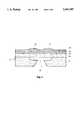
- FIG. 2is a cross-sectional view of the pressure sensor utilized in accordance with the preferred embodiment of the invention. It illustrates the semiconductor materials which can be used in the fabrication of the sensor.
- the base of sensor 10can consist of a single crystalline silicon substrate 12 having a cavity 24.
- Layer 14serves as the sensing diaphragm.
- Layers 16 and 18are deposited onto layer 14 forming a composite dielectric isolation layer. Layer 16 is deposited onto layer 14 and can be a 500 angstroms thick layer of silicon dioxide.
- Layer 18a layer of LPCVD silicon nitride, approximately 900 angstroms thick, can be deposited onto layer 16.
- Layers 16 and 18form a composite dielectric isolation upon which the resistors will be placed. These layers serve to isolate the resistors minimizing both unwanted leakage currents and resistance degradation at high process fluid temperatures.
- Layer 22is the sensing resistor material which can be deposited through LPCVD polysilicon deposition onto the dielectric isolation layer 18.
- Layer 20can be a layer of LPCVD silicon nitrate deposited over the sensing resistors 22 and layer 18, and serves as a passivation layer.
- Cavity 24is positioned on the reverse side of sensing diaphragm 14. It is vacuum filled when used to measure absolute pressure and vented to the atmosphere for a gauge pressure measurement. When a differential pressure measurement is warranted, different pressures are applied across sensing diaphragm 14.
- Sensing diaphragm 14senses the relative pressure of the process flow and produces a corresponding electrical signal.
- Sensing circuitrycan be disposed on the diaphragm with a dielectric layer interposed between.
- the sensing circuitrycan consist of four piezoresistors formed from layer 22 positioned symmetrically about the diaphragm center and connected in series to provide the highest pressure sensitivity and the best matching of resistors from diaphragm to diaphragm.
- Metalized pads 26are connected to the ends of the piezoresistors 22 for providing external electrical connection, and to transmit the electrical signal produced by the piezoresistors to further signal processing circuitry (not shown).
- micro-controller 30produces a AC waveform 32 which is applied to electrically powered pressure sensing bridge 38.
- pressure sensing bridge 38responds to the pressure applied to it thereby generating signal 46a & 46b representing a measurement of it.
- the bridge output signal 46a & 46bcan then be transmitted to a normalization and sequence circuit 52.
- Circuit 52normalizes the bridge output signal as well as sequences all the various electrical signals 56a, 56b & 56c generated within the sensor.
- Bridge output signal 46a & 46bcan be normalized by comparing signals 46a, 46b to an output of a similarly excited reference voltage divider thereby essentially eliminating the effect of errors and drift in the conditioning and digitization circuitry.
- the resulting normalized signal and all other electronic signals 56a, 56b & 56c generated within the sensorare sequenced. Examples of such signals can be calibration signals used for calibrating the A/D converter, and temperature signals indicating the process fluid temperature as well as the circuitry temperature. This sequencing minimizes the effects of amplifier and sensor noise while maintaining adequate speed of response to changes in the input pressure as well as environmental influences such as ambient temperature.
- the resulting normalized signal 54can then be amplified at amplification stage 42 producing signal 48.
- Amplified signal 48can be transmitted to an analog-to-digital converter 44 to produce an equivalent digital signal 50 of the pressure measurement signal, 46a & 46b.
- Digital signal 50can then be transmitted to other signal processing circuitry for further signal conditioning and processing. Normalization and sequencing circuit 52, amplication circuit 42, and A/D converter 44 are all under the control of micro-controller 30.
- Voltage excitationcan be utilized with a clock-pulse voltage signal 32 providing bipolar AC excitation.
- the clock-pulse voltage signal 32can be generated from a micro-controller 30.
- this inventionis not limited to voltage excitation.
- Bipolar current excitation methodscan be used as well.
- Voltage signal 32can be a 50% duty-cycle square-wave pulse having an amplitude, Vex, of less than 10 volts, preferably 3 volts, and a frequency less than 100K Hz, preferably between 5-10 Hz.
- Inverter 34aapplies excitation voltage, Vex, 36a, to the first input terminal, 40a, of sensing element, 38.
- Inverter 34bapplies a similar voltage of opposite polarity, -Vex, 36b, to the second input terminal, 40b of sensing element, 38.
- the amplitude and frequency valuesare chosen to achieve micro-power consumption in the order of less than 10 mW.
- Low power consumptionis crucial for industrial instruments since they need to adhere to industrial instrumentation intrinsic safety requirements such as the CENELEC Intrinsic Safety Standard for Electrical Apparatus for Potentially Explosive Atmospheres, EN50020.
- the circuitconsumes approximately 1 mW of power which is advantageous since pressure devices of this type are generally powered by a two-wire circuit that supplies both the energy to operate the device and carries the data transmission.
- FIG. 5illustrates the sensing circuitry that can be employed by pressure sensing bridge 38.
- the sensing circuitrycan consist of four piezoresistive elements positioned in a Wheatstone bridge configuration.
- the Wheatstone bridgehas two arms, one containing piezoresistors 28a and 28b connected in series and a second arm containing piezoresistors 28c and 28d connected in series. Both arms of the bridge are electrically connected with input terminals 40a and 40b.
- the four piezoresistors 28a, 28b, 28c, and 28dare positioned on the sensing diaphragm such that when they are subject to movement of the sensing diaphragms due to pressure, piezoresistors 28b and 28c both experience either a compressive or a tensile strain while piezoresistors 28a and 28d simultaneously experience the opposite strain.
- piezoresistors 28a and 28dare increasing in resistance
- piezoresistors 28c and 28dare decreasing in resistance.
- Voltage V2can be expressed mathematically in accord with the following mathematical relation:
- Vexis the excitation voltage
- Vintis an interference signal attributable to low-frequency or dc component noises
- ⁇ ris the change in resistance ratio (i.e., unit or normalized resistance) across both arms of the Wheatstone bridge.
- the change in resistance ratiois the change in resistance of the wheatstone bridge divided by the initial resistance of the wheatstone bridge.
- Micro-controller 30generates a clock-pulse voltage signal 32.
- Voltage signal 32can be a 50% duty-cycle square-wave pulse having an amplitude, Vex, of less than 10 volts, preferably 3 volts, and a frequency less than 100K Hz, preferably between 5-10 Hz.
- a first voltage, Vex, 36ais applied to input terminal 40a of sensing element 38 having an identical amplitude and frequency as clock-pulse signal 32.
- pressureis applied to the sensing diaphragm, it deflects causing one of the piezoresistors on each arm of the bridge to increase in resistance while the other piezoresistors decreases in resistance. This imbalance across the bridge causes the voltage V2' to be related to the pressure sensed in accord with the following mathematical relation:
- V2'The measurement of V2' is made during the first half of the application of voltage 36a. For example, in the case where Vex is applied to input terminal 36a at a frequency of 10 Hz, the width of the clock-pulse voltage 40a is approximately 100 ms. For the first 50 ms, V2', 46, is measured. During the remaining 50 ms, the signal 46 is amplified by amplification stage 42. At the completion of the application of voltage 36a, the amplified signal 48 is transmitted to A/D converter 44 which generates an equivalent digital signal 50 which is then transmitted for further signal processing.
- a second voltage, -Vex, 36bis applied to input terminal 40b which is substantially similar to the first voltage but opposite in polarity.
- V2the voltage V2" to be related to the pressure sensed in accord with the following mathematical relation:
- V2The measurement of V2" is made in the same fashion as V2'. During the first half of the application of voltage 36b, the measurement of V2" is made generating signal 46. During the second half of the application of voltage 36b, signal 46 is amplified for transmission to A/D converter 44. An equivalent digital signal 50 is generated from A/D converter 44 and transmitted to further electronic circuitry for additional signal processing.
- the signal processing circuitrymay take the difference between these two measurements and eliminate the interference noise signal and produce a resultant resistance as follows:
- This resulting resistance ratio ( ⁇ r)is directly proportional to the pressure sensed and is used as a measurement for it.
- the above described inventiondiscloses an apparatus and method for providing micro-power excitation of polysilicon piezoresistor sensing elements that utilize a polysilicon diaphragm.
- the inventionis beneficial since experimental results show that it prevents the long term transient behavior of polysilicon piezoresistors upon electrical activation.
- the voltage levels and the frequency rangesare chosen so that the circuit employs micro-power consumption of approximately 1 mW and minimal transient behavior upon activation.
- each input of the wheatstone bridgealternates between a positive voltage (V ex ) and zero volts (when viewed from a single reference point).
- each input (40a, 40b)is 180 degrees out of phase from the other input. Therefore, when input 40a is at V ex , input 40b is at zero volts, while when input 40b is at V ex , input 40a is at zero volts.
- Each leg of the wheatstone bridgeis therfore alternatively energized by a differential excitation source. Since each leg is energized with a positive voltage, while the other let is kept at a zero volt potential, a common zero volt reference point is maintained with reaspect to the normalization and sequencing circuitry (e.g., FIG. 1--element 52).
Landscapes
- Physics & Mathematics (AREA)
- General Physics & Mathematics (AREA)
- Measuring Fluid Pressure (AREA)
- Pressure Sensors (AREA)
Abstract
Description
V2=Δ.sub.r Vex+Vint (1)
V2'=(Δr)Vex+Vint (2)
V2"=(Δr)(-Vex)+Vint (3)
Δ.sub.r =(V2'-V2")/(2V.sub.ex)
Claims (24)
Priority Applications (1)
| Application Number | Priority Date | Filing Date | Title |
|---|---|---|---|
| US08/734,088US5681997A (en) | 1994-12-20 | 1996-06-19 | Excitation of polysilicon based piezoresistive pressure sensors |
Applications Claiming Priority (2)
| Application Number | Priority Date | Filing Date | Title |
|---|---|---|---|
| US35996294A | 1994-12-20 | 1994-12-20 | |
| US08/734,088US5681997A (en) | 1994-12-20 | 1996-06-19 | Excitation of polysilicon based piezoresistive pressure sensors |
Related Parent Applications (1)
| Application Number | Title | Priority Date | Filing Date |
|---|---|---|---|
| US35996294AContinuation | 1994-12-20 | 1994-12-20 |
Publications (1)
| Publication Number | Publication Date |
|---|---|
| US5681997Atrue US5681997A (en) | 1997-10-28 |
Family
ID=23415996
Family Applications (1)
| Application Number | Title | Priority Date | Filing Date |
|---|---|---|---|
| US08/734,088Expired - Fee RelatedUS5681997A (en) | 1994-12-20 | 1996-06-19 | Excitation of polysilicon based piezoresistive pressure sensors |
Country Status (6)
| Country | Link |
|---|---|
| US (1) | US5681997A (en) |
| EP (1) | EP0799412B1 (en) |
| JP (1) | JPH10511459A (en) |
| CA (1) | CA2207020C (en) |
| DE (1) | DE69528775T2 (en) |
| WO (1) | WO1996019719A1 (en) |
Cited By (24)
| Publication number | Priority date | Publication date | Assignee | Title |
|---|---|---|---|---|
| US6247369B1 (en) | 1995-04-04 | 2001-06-19 | The United States Of America As Represented By The Administrator Of The National Aeronautics Of Space Administration | Multi-channel electronically scanned cryogenic pressure sensor and method for making same |
| WO2001061298A1 (en)* | 2000-02-15 | 2001-08-23 | Breed Automotive Technology, Inc. | Alternating voltage with resistance pressure sensor |
| US6433524B1 (en) | 2001-03-15 | 2002-08-13 | Rosemount Aerospace Inc. | Resistive bridge interface circuit |
| US6453748B1 (en)* | 1999-12-15 | 2002-09-24 | Wayne State University | Boron nitride piezoresistive device |
| US6472244B1 (en) | 1996-07-31 | 2002-10-29 | Sgs-Thomson Microelectronics S.R.L. | Manufacturing method and integrated microstructures of semiconductor material and integrated piezoresistive pressure sensor having a diaphragm of polycrystalline semiconductor material |
| US6504226B1 (en) | 2001-12-20 | 2003-01-07 | Stmicroelectronics, Inc. | Thin-film transistor used as heating element for microreaction chamber |
| US20030006948A1 (en)* | 2001-07-09 | 2003-01-09 | Hyeon-Ho Son | Liquid crystal display device and driving method for the same |
| US6529847B2 (en)* | 2000-01-13 | 2003-03-04 | The Foxboro Company | Multivariable transmitter |
| WO2002052253A3 (en)* | 2000-12-27 | 2003-03-06 | Rosemount Analytical Inc | PROCESS FOR MINIMIZING CROSS-TALK IN DIAGNOSTIC SIGNALS OF A pH SENSOR |
| WO2003052369A1 (en)* | 2001-12-18 | 2003-06-26 | Honeywell International Inc. | Sensor formed on silicon on insulator structure and having reduced power up drift |
| US20030116552A1 (en)* | 2001-12-20 | 2003-06-26 | Stmicroelectronics Inc. | Heating element for microfluidic and micromechanical applications |
| EP1324013A1 (en)* | 2001-12-26 | 2003-07-02 | Seiko Instruments Inc. | Pressure measuring apparatus |
| US20040255682A1 (en)* | 2003-06-18 | 2004-12-23 | Petrova Roumiana S. | Flexible thin film pressure sensor |
| EP1319935A3 (en)* | 2001-12-11 | 2005-08-03 | Parker Hannifin GmbH | Signal processing arrangement for a pressure switch or the like |
| US20050274168A1 (en)* | 2004-06-11 | 2005-12-15 | Robert Bosch Corporation Gmbh | Hybrid impact sensor |
| US20050275047A1 (en)* | 2004-06-11 | 2005-12-15 | Robert Bosch Gmbh | Stress wave sensor |
| US20070202012A1 (en)* | 2003-11-12 | 2007-08-30 | Steichen John C | System and method for sensing and analyzing gases |
| WO2007095410A3 (en)* | 2006-02-14 | 2007-12-13 | Electrojet Inc | Engine timing control with intake air pressure sensor |
| EP1785709A3 (en)* | 2005-11-10 | 2008-07-02 | Honeywell International Inc. | Method and system of providing power to a pressure and temperature sensing element |
| US20130145854A1 (en)* | 2011-12-08 | 2013-06-13 | Kulite Semiconductor Products, Inc. | Linked bridge pressure transducer assemblies |
| US20130215056A1 (en)* | 2012-02-20 | 2013-08-22 | Sony Mobile Communications Ab | Method for determining a sensor value and sensor system |
| US20130222306A1 (en)* | 2012-02-28 | 2013-08-29 | Sony Mobile Communications Ab | Electronic device and method for determining a temperature of an electronic device |
| US9909944B2 (en) | 2013-06-11 | 2018-03-06 | Danfoss A/S | Thin film sensor |
| EP3961175A4 (en)* | 2019-04-26 | 2022-06-22 | Nagano Keiki Co., Ltd. | PRESSURE SENSOR |
Families Citing this family (5)
| Publication number | Priority date | Publication date | Assignee | Title |
|---|---|---|---|---|
| DE19741428A1 (en)* | 1997-09-19 | 1999-04-01 | Siemens Ag | Semiconductor sensor with a base body and at least one deformation body |
| JP5299254B2 (en)* | 2009-12-14 | 2013-09-25 | 三菱電機株式会社 | Semiconductor pressure sensor and manufacturing method thereof |
| CN102023066B (en)* | 2010-05-31 | 2012-07-18 | 昆山双桥传感器测控技术有限公司 | Universal pressure sensor of automobile |
| DE102023205187A1 (en) | 2023-06-02 | 2024-12-05 | Infineon Technologies Ag | SENSOR DEVICE FOR MEASURING A GAS CONCENTRATION AND METHOD FOR DETERMINING A GAS CONCENTRATION |
| DE102023208932A1 (en) | 2023-09-14 | 2025-03-20 | Infineon Technologies Ag | IMPROVED OFFSET COMPENSATION TECHNIQUE FOR THERMAL CONDUCTIVITY MEASUREMENT OF A GAS CONCENTRATION SENSOR |
Citations (12)
| Publication number | Priority date | Publication date | Assignee | Title |
|---|---|---|---|---|
| US4233848A (en)* | 1978-01-06 | 1980-11-18 | Hitachi, Ltd. | Strain gauge pressure transducer apparatus having an improved impedance bridge |
| EP0139370A1 (en)* | 1983-08-12 | 1985-05-02 | Prutec Limited | Piezoresistive transducer |
| US4659235A (en)* | 1985-04-16 | 1987-04-21 | Borg-Warner Automotive, Inc. | Fluid pressure sensor with temperature indication |
| US4672354A (en)* | 1985-12-05 | 1987-06-09 | Kulite Semiconductor Products, Inc. | Fabrication of dielectrically isolated fine line semiconductor transducers and apparatus |
| US4765188A (en)* | 1986-11-24 | 1988-08-23 | Bourns Instruments, Inc. | Pressure transducer with integral digital temperature compensation |
| US4853669A (en)* | 1985-04-26 | 1989-08-01 | Wisconsin Alumni Research Foundation | Sealed cavity semiconductor pressure transducers and method of producing the same |
| US4966034A (en)* | 1988-04-28 | 1990-10-30 | Schrader Automotive, Inc. | On-board tire pressure indicating system performing temperature-compensated pressure measurement, and pressure measurement circuitry thereof |
| EP0482487A2 (en)* | 1990-10-25 | 1992-04-29 | Becton, Dickinson and Company | Apparatus and method for a temperature compensation of a pressure transducer |
| US5209118A (en)* | 1989-04-07 | 1993-05-11 | Ic Sensors | Semiconductor transducer or actuator utilizing corrugated supports |
| US5220838A (en)* | 1991-03-28 | 1993-06-22 | The Foxboro Company | Overpressure-protected, differential pressure sensor and method of making the same |
| EP0590292A2 (en)* | 1992-10-01 | 1994-04-06 | Motorola, Inc. | Pulsed pressure sensor circuit and method therefor |
| WO1994009376A1 (en)* | 1992-10-16 | 1994-04-28 | Rosemount Analytical Inc. | Circuit for measuring source resistance of a sensor |
- 1995
- 1995-12-15JPJP8519873Apatent/JPH10511459A/enactivePending
- 1995-12-15EPEP95943086Apatent/EP0799412B1/ennot_activeExpired - Lifetime
- 1995-12-15CACA002207020Apatent/CA2207020C/ennot_activeExpired - Fee Related
- 1995-12-15WOPCT/US1995/016200patent/WO1996019719A1/enactiveIP Right Grant
- 1995-12-15DEDE69528775Tpatent/DE69528775T2/ennot_activeExpired - Fee Related
- 1996
- 1996-06-19USUS08/734,088patent/US5681997A/ennot_activeExpired - Fee Related
Patent Citations (13)
| Publication number | Priority date | Publication date | Assignee | Title |
|---|---|---|---|---|
| US4233848A (en)* | 1978-01-06 | 1980-11-18 | Hitachi, Ltd. | Strain gauge pressure transducer apparatus having an improved impedance bridge |
| EP0139370A1 (en)* | 1983-08-12 | 1985-05-02 | Prutec Limited | Piezoresistive transducer |
| US4659235A (en)* | 1985-04-16 | 1987-04-21 | Borg-Warner Automotive, Inc. | Fluid pressure sensor with temperature indication |
| US4853669A (en)* | 1985-04-26 | 1989-08-01 | Wisconsin Alumni Research Foundation | Sealed cavity semiconductor pressure transducers and method of producing the same |
| US4672354A (en)* | 1985-12-05 | 1987-06-09 | Kulite Semiconductor Products, Inc. | Fabrication of dielectrically isolated fine line semiconductor transducers and apparatus |
| US4765188A (en)* | 1986-11-24 | 1988-08-23 | Bourns Instruments, Inc. | Pressure transducer with integral digital temperature compensation |
| US4966034A (en)* | 1988-04-28 | 1990-10-30 | Schrader Automotive, Inc. | On-board tire pressure indicating system performing temperature-compensated pressure measurement, and pressure measurement circuitry thereof |
| US5209118A (en)* | 1989-04-07 | 1993-05-11 | Ic Sensors | Semiconductor transducer or actuator utilizing corrugated supports |
| EP0482487A2 (en)* | 1990-10-25 | 1992-04-29 | Becton, Dickinson and Company | Apparatus and method for a temperature compensation of a pressure transducer |
| US5220838A (en)* | 1991-03-28 | 1993-06-22 | The Foxboro Company | Overpressure-protected, differential pressure sensor and method of making the same |
| EP0590292A2 (en)* | 1992-10-01 | 1994-04-06 | Motorola, Inc. | Pulsed pressure sensor circuit and method therefor |
| US5351549A (en)* | 1992-10-01 | 1994-10-04 | Motorola, Inc. | Pulsed pressure sensor circuit and method therefor |
| WO1994009376A1 (en)* | 1992-10-16 | 1994-04-28 | Rosemount Analytical Inc. | Circuit for measuring source resistance of a sensor |
Cited By (40)
| Publication number | Priority date | Publication date | Assignee | Title |
|---|---|---|---|---|
| US6247369B1 (en) | 1995-04-04 | 2001-06-19 | The United States Of America As Represented By The Administrator Of The National Aeronautics Of Space Administration | Multi-channel electronically scanned cryogenic pressure sensor and method for making same |
| US6472244B1 (en) | 1996-07-31 | 2002-10-29 | Sgs-Thomson Microelectronics S.R.L. | Manufacturing method and integrated microstructures of semiconductor material and integrated piezoresistive pressure sensor having a diaphragm of polycrystalline semiconductor material |
| US6453748B1 (en)* | 1999-12-15 | 2002-09-24 | Wayne State University | Boron nitride piezoresistive device |
| US6529847B2 (en)* | 2000-01-13 | 2003-03-04 | The Foxboro Company | Multivariable transmitter |
| WO2001061298A1 (en)* | 2000-02-15 | 2001-08-23 | Breed Automotive Technology, Inc. | Alternating voltage with resistance pressure sensor |
| US6427540B1 (en) | 2000-02-15 | 2002-08-06 | Breed Automotive Technology, Inc. | Pressure sensor system and method of excitation for a pressure sensor |
| WO2002052253A3 (en)* | 2000-12-27 | 2003-03-06 | Rosemount Analytical Inc | PROCESS FOR MINIMIZING CROSS-TALK IN DIAGNOSTIC SIGNALS OF A pH SENSOR |
| US6433524B1 (en) | 2001-03-15 | 2002-08-13 | Rosemount Aerospace Inc. | Resistive bridge interface circuit |
| US20030006948A1 (en)* | 2001-07-09 | 2003-01-09 | Hyeon-Ho Son | Liquid crystal display device and driving method for the same |
| US7085657B2 (en) | 2001-12-11 | 2006-08-01 | Parker Hannifin Gmbh | Signal processing unit for a pressure switch or the like |
| EP1319935A3 (en)* | 2001-12-11 | 2005-08-03 | Parker Hannifin GmbH | Signal processing arrangement for a pressure switch or the like |
| CN1307412C (en)* | 2001-12-18 | 2007-03-28 | 霍尼韦尔国际公司 | Sensors formed on silicon-on-insulator structures with reduced power-on drift |
| WO2003052369A1 (en)* | 2001-12-18 | 2003-06-26 | Honeywell International Inc. | Sensor formed on silicon on insulator structure and having reduced power up drift |
| US6504226B1 (en) | 2001-12-20 | 2003-01-07 | Stmicroelectronics, Inc. | Thin-film transistor used as heating element for microreaction chamber |
| US7056795B2 (en) | 2001-12-20 | 2006-06-06 | Stmicroelectronics, Inc. | Thin-film transistor used as heating element for microreaction chamber |
| US6864140B2 (en) | 2001-12-20 | 2005-03-08 | Stmicroelectronics, Inc. | Thin-film transistor used as heating element for microreaction chamber |
| US20070284360A1 (en)* | 2001-12-20 | 2007-12-13 | Stmicroelectronics Inc. | Heating element for microfluidic and micromechanical applications |
| US20050136598A1 (en)* | 2001-12-20 | 2005-06-23 | Stmicroelectronics Inc. | Thin-film transistor used as heating element for microreaction chamber |
| US20030116552A1 (en)* | 2001-12-20 | 2003-06-26 | Stmicroelectronics Inc. | Heating element for microfluidic and micromechanical applications |
| US9012810B2 (en) | 2001-12-20 | 2015-04-21 | Stmicroelectronics, Inc. | Heating element for microfluidic and micromechanical applications |
| EP1324013A1 (en)* | 2001-12-26 | 2003-07-02 | Seiko Instruments Inc. | Pressure measuring apparatus |
| US6820492B2 (en) | 2001-12-26 | 2004-11-23 | Seiko Instruments Inc. | Pressure measuring apparatus |
| US20040255682A1 (en)* | 2003-06-18 | 2004-12-23 | Petrova Roumiana S. | Flexible thin film pressure sensor |
| US7082834B2 (en)* | 2003-06-18 | 2006-08-01 | New Jersey Institute Of Technology | Flexible thin film pressure sensor |
| WO2004113858A3 (en)* | 2003-06-18 | 2005-06-02 | New Jersey Tech Inst | Flexible thin film pressure sensor |
| US7763208B2 (en)* | 2003-11-12 | 2010-07-27 | E.I. Du Pont De Nemours And Company | System and method for sensing and analyzing gases |
| US20070202012A1 (en)* | 2003-11-12 | 2007-08-30 | Steichen John C | System and method for sensing and analyzing gases |
| US20050275047A1 (en)* | 2004-06-11 | 2005-12-15 | Robert Bosch Gmbh | Stress wave sensor |
| US7231803B2 (en) | 2004-06-11 | 2007-06-19 | Robert Bosch Gmbh | Hybrid impact sensor |
| US7188511B2 (en) | 2004-06-11 | 2007-03-13 | Robert Bosch Gmbh | Stress wave sensor |
| US20050274168A1 (en)* | 2004-06-11 | 2005-12-15 | Robert Bosch Corporation Gmbh | Hybrid impact sensor |
| EP1785709A3 (en)* | 2005-11-10 | 2008-07-02 | Honeywell International Inc. | Method and system of providing power to a pressure and temperature sensing element |
| WO2007095410A3 (en)* | 2006-02-14 | 2007-12-13 | Electrojet Inc | Engine timing control with intake air pressure sensor |
| EP1984621A4 (en)* | 2006-02-14 | 2018-12-05 | Electrojet, Inc. | Engine timing control with intake air pressure sensor |
| US20130145854A1 (en)* | 2011-12-08 | 2013-06-13 | Kulite Semiconductor Products, Inc. | Linked bridge pressure transducer assemblies |
| US8910524B2 (en)* | 2011-12-08 | 2014-12-16 | Kulite Semiconductor Products, Inc. | Linked bridge pressure transducer assemblies |
| US20130215056A1 (en)* | 2012-02-20 | 2013-08-22 | Sony Mobile Communications Ab | Method for determining a sensor value and sensor system |
| US20130222306A1 (en)* | 2012-02-28 | 2013-08-29 | Sony Mobile Communications Ab | Electronic device and method for determining a temperature of an electronic device |
| US9909944B2 (en) | 2013-06-11 | 2018-03-06 | Danfoss A/S | Thin film sensor |
| EP3961175A4 (en)* | 2019-04-26 | 2022-06-22 | Nagano Keiki Co., Ltd. | PRESSURE SENSOR |
Also Published As
| Publication number | Publication date |
|---|---|
| JPH10511459A (en) | 1998-11-04 |
| EP0799412A1 (en) | 1997-10-08 |
| CA2207020A1 (en) | 1996-06-27 |
| WO1996019719A1 (en) | 1996-06-27 |
| CA2207020C (en) | 2003-12-30 |
| DE69528775D1 (en) | 2002-12-12 |
| EP0799412B1 (en) | 2002-11-06 |
| DE69528775T2 (en) | 2003-07-03 |
Similar Documents
| Publication | Publication Date | Title |
|---|---|---|
| US5681997A (en) | Excitation of polysilicon based piezoresistive pressure sensors | |
| US4986127A (en) | Multi-functional sensor | |
| US4233848A (en) | Strain gauge pressure transducer apparatus having an improved impedance bridge | |
| US7503221B2 (en) | Dual span absolute pressure sense die | |
| EP0579226B1 (en) | Force transducer and pressure detecting circuit using the same | |
| US20070018650A1 (en) | MEMS Based Conductivity-Temperature-Depth Sensor for Harsh Oceanic Environment | |
| EP0198855A1 (en) | Circuit for capacitive sensor made of brittle material | |
| USRE34694E (en) | Automatic transducer selection system for pressure measurement | |
| CA1309878C (en) | Dual sided pressure sensor | |
| US7705583B2 (en) | Micro-electromechanical system (MEMS) based current and magnetic field sensor | |
| CN110441551B (en) | Atomic force probe type sensor based on quartz ring resonator | |
| WO1996022515A1 (en) | Apparatus for detection of a diaphragm rupture in a pressure sensor | |
| EP0139370A1 (en) | Piezoresistive transducer | |
| JPH02242121A (en) | Pressure/temperature compound detector | |
| JPH08226862A (en) | Sensor and method for performing temperature compensation for measuring-range fluctuation in sensor thereof | |
| RU2096785C1 (en) | Compensation accelerator | |
| JPS58117433A (en) | Pressure measuring device | |
| US4120195A (en) | Method of using embedded normal stress sensors in propellant grains | |
| JP2694594B2 (en) | Pressure sensor | |
| WO1998015809A1 (en) | Semiconductor sensor having diagnostic function and diagnostic method for semiconductor sensor | |
| JPH04307331A (en) | Complex sensor | |
| Kapels et al. | Monolithic surface-micromachined sensor system for high pressure applications | |
| JPH06102128A (en) | Semiconductor multi-function sensor | |
| Marioli et al. | Strain gauge transducers: an evaluation of accuracy limits | |
| Nie et al. | A micro and low-cost packaging technology of high accuracy piezoresistive pressure sensors with Parylene coating |
Legal Events
| Date | Code | Title | Description |
|---|---|---|---|
| FPAY | Fee payment | Year of fee payment:4 | |
| AS | Assignment | Owner name:INVENSYS SYSTEMS INC. (FORMERLY KNOWN AS THE FOXBO Free format text:CHANGE OF NAME;ASSIGNOR:FOXBORO COMPANY, THE;REEL/FRAME:015328/0762 Effective date:20010330 | |
| AS | Assignment | Owner name:DEUTSCHE BANK AG, LONDON, UNITED KINGDOM Free format text:SECURITY INTEREST;ASSIGNOR:INVENSYS SYSTEMS, INC.;REEL/FRAME:015279/0874 Effective date:20040401 Owner name:DEUTSCHE BANK AG, LONDON,UNITED KINGDOM Free format text:SECURITY INTEREST;ASSIGNOR:INVENSYS SYSTEMS, INC.;REEL/FRAME:015279/0874 Effective date:20040401 | |
| LAPS | Lapse for failure to pay maintenance fees | ||
| STCH | Information on status: patent discontinuation | Free format text:PATENT EXPIRED DUE TO NONPAYMENT OF MAINTENANCE FEES UNDER 37 CFR 1.362 | |
| FP | Lapsed due to failure to pay maintenance fee | Effective date:20051028 | |
| AS | Assignment | Owner name:INVENSYS SYSTEMS, INC., MASSACHUSETTS Free format text:RELEASE AND TERMINATION OF SECURITY INTEREST IN PA;ASSIGNOR:DEUTSCHE BANK AG LONDON;REEL/FRAME:018367/0749 Effective date:20060727 |