US5677648A - Noise compensated phase locked loop circuit - Google Patents
Noise compensated phase locked loop circuitDownload PDFInfo
- Publication number
- US5677648A US5677648AUS08/396,834US39683495AUS5677648AUS 5677648 AUS5677648 AUS 5677648AUS 39683495 AUS39683495 AUS 39683495AUS 5677648 AUS5677648 AUS 5677648A
- Authority
- US
- United States
- Prior art keywords
- locked loop
- phase
- phase locked
- input lines
- state
- Prior art date
- Legal status (The legal status is an assumption and is not a legal conclusion. Google has not performed a legal analysis and makes no representation as to the accuracy of the status listed.)
- Expired - Lifetime
Links
Images


Classifications
- H—ELECTRICITY
- H03—ELECTRONIC CIRCUITRY
- H03L—AUTOMATIC CONTROL, STARTING, SYNCHRONISATION OR STABILISATION OF GENERATORS OF ELECTRONIC OSCILLATIONS OR PULSES
- H03L7/00—Automatic control of frequency or phase; Synchronisation
- H—ELECTRICITY
- H03—ELECTRONIC CIRCUITRY
- H03L—AUTOMATIC CONTROL, STARTING, SYNCHRONISATION OR STABILISATION OF GENERATORS OF ELECTRONIC OSCILLATIONS OR PULSES
- H03L7/00—Automatic control of frequency or phase; Synchronisation
- H03L7/06—Automatic control of frequency or phase; Synchronisation using a reference signal applied to a frequency- or phase-locked loop
- H03L7/08—Details of the phase-locked loop
- H03L7/085—Details of the phase-locked loop concerning mainly the frequency- or phase-detection arrangement including the filtering or amplification of its output signal
- H03L7/089—Details of the phase-locked loop concerning mainly the frequency- or phase-detection arrangement including the filtering or amplification of its output signal the phase or frequency detector generating up-down pulses
- H03L7/0891—Details of the phase-locked loop concerning mainly the frequency- or phase-detection arrangement including the filtering or amplification of its output signal the phase or frequency detector generating up-down pulses the up-down pulses controlling source and sink current generators, e.g. a charge pump
- Y—GENERAL TAGGING OF NEW TECHNOLOGICAL DEVELOPMENTS; GENERAL TAGGING OF CROSS-SECTIONAL TECHNOLOGIES SPANNING OVER SEVERAL SECTIONS OF THE IPC; TECHNICAL SUBJECTS COVERED BY FORMER USPC CROSS-REFERENCE ART COLLECTIONS [XRACs] AND DIGESTS
- Y10—TECHNICAL SUBJECTS COVERED BY FORMER USPC
- Y10S—TECHNICAL SUBJECTS COVERED BY FORMER USPC CROSS-REFERENCE ART COLLECTIONS [XRACs] AND DIGESTS
- Y10S331/00—Oscillators
- Y10S331/02—Phase locked loop having lock indicating or detecting means
Definitions
- a Phase Locked Loopis commonly used to synthesize an output frequency by synchronizing an input signal, known as the reference signal, with an internal oscillator.
- a PLLcommonly consists of a phase detector, a filter and a reference oscillator.
- the oscillator outputwill be at the reference frequency scaled by M/N.
- M/Nis equal to one, there are no digital dividers in either path.
- the PLLWhen the difference between the input and reference oscillator frequencies is zero, or very small, the PLL is said to be in a locked state. When there is a difference in the frequencies, either when the locked state is perturbed or when the reference input changes frequency, the PLL moves to a dynamic state in which the oscillator frequency is adjusted until the locked state is achieved once more.
- the Phase Detectorproduces a signal indicative of the phase difference between the inputs of the PD; that is the input signal and the oscillator signal.
- the PD detectorcan be implemented in many ways, with each incarnation having unique characteristics.
- a very common PD circuitis a digital, phase-frequency comparator, with a three-state output. This particular type of PD is referred to as a type-II phase detector.
- Type-II phase detectorsare used in applications where frequency lock as well as phase lock is desirable.
- Type-II phase detectorsare usually associated with a charge pump device, which translates the three-state output of the PD into a signal which is filtered before controlling the internal oscillator.
- the three output states of the PDare denoted by UP, DOWN and NEITHER.
- UPthe charge pump allows current to flow into the input of the filter.
- DOWNthe charge pump removes current from the input of the filter.
- NEITHERno current flows.
- the filter in a PLLprovides a voltage to the internal oscillator which affects the frequency of the oscillator.
- the most simple form of filteris a capacitor.
- the capacitoracts as an integrator, accumulating the net charge output by the charge pump circuit, resulting in a stable voltage which can be used to control an internal oscillator.
- Such an oscillatoris known as a Voltage Controlled Oscillator (VCO).
- VCOVoltage Controlled Oscillator
- the PDWhen the PLL is in a dynamic state, the PD generates many UP, DOWN and NEITHER output states as the loop attempts to acquire lock. When the loop is in lock, the PD generates only NEITHER output, since no correction is necessary by definition. This means that in the quiescent, locked state the loop has no gain, and in particular the charge pump is not driving any current. A signal that is not driven is known as a high impedance signal, and is very susceptible to picking up all types of extraneous noise.
- a companion technique often used to lessen the effect of the inherent variation of shieldingis the use of a differential filter.
- Differential filtersonly filter the difference between two signals. This means that if some noise couples onto both inputs in an identical manner, the difference is not changed and hence the noise has no effect.
- a signal that adds onto both signals which are subsequently subtractedis known as a common-mode signal, since it is common to both signals.
- the present inventionrelates to a PLL using a type-II phase detector, a charge pump device, a logic circuit, a differential filter and a VCO.
- the PLLmay also use digital dividers.
- the phase detectorcontrols a logic circuit which ensures that any occurrence of uncorrelated noise, from any source, is common-mode to the inputs of the differential filter when the PLL is in a locked state.
- the inputs to the differential filterare connected via a transistor and a join line, resulting in the two inputs becoming a single node. This ensures that any noise is guaranteed to be common-mode to the filter, and as such will not affect the VCO input. If the NEITHER output is due to the PLL being in a locked state, the absence of a perturbation to the VCO input will cause the PLL to continue to operate in the locked state.
- the PLLis no longer sensitive to erroneous signals that could cause it to go into an unlocked, dynamic state from a previously locked state.
- This "shielding"is inexpensive because both the logic device and the transistor are already available on the integrated circuit, and no additional space or materials must be used.
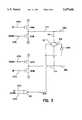
- FIG. 1shows a digital PLL including a charge pump device, embodying the present invention.
- FIG. 2shows an expanded view of the logic device controlling the charge pump device, embodying the present invention.
- FIG. 3shows an expanded view of an alternate embodiment of the invention.
- a PLLcontains a minimum of three elements; a phase detector (PD), a filter and a voltage controlled oscillator (VCO).
- the VCO outputis the internal oscillator signal being generated by the PLL, and is the signal that is compared with the input reference signal.
- the input signal u 1 and the VCO signal u 2are fed into the phase-frequency detector 105 via lines 101 and 103 respectively.
- the PD 105produces a signal based on the differences between the phase and frequency of the input signal and the VCO signal.
- a type-II PDwill produce an UP output state when the internal oscillator, the VCO, has to increase in frequency.
- the UP output stateconsists of the logic element 1 on the UP line 107a and the logic element 0 on the DOWN line 107b.
- a type-II PDwill produce a DOWN output state when the internal oscillator has to decrease the frequency of the VCO.
- a DOWN output stateconsists of the logic element 0 on the UP line 107a and the logic element 1 on the DOWN line 107b.
- the type-II PDwill produce a NEITHER output state, consisting of the logic element 0 on both the UP line 107a and the DOWN line 107b.
- the UP and DOWN lines 107a and 107bare then fed into a charge pump device 109.
- the charge pump devicetransforms the UP or DOWN output states into a net charge movement to or from the differential filter 117. The details of this procedure are described below.
- An UP or DOWN output statewill result in the voltage difference between lines 111a and 111b to pass on to lines 113a and 113b respectively. If the PD output is NEITHER, then the NOR gate 116 will close transistor 115, and a join line 116 will join lines 113aand 113b, causing there to be no voltage difference between lines 113a and 113b.
- a NEITHER outputis the output state produced by the PD when the PLL is in a locked state, that is a state where there is no phase difference between the input and the VCO.
- the locked statethere should be no voltage difference between lines 113a and 113b. If there were a voltage difference, the output of differential filter 117, on lines 119a and 119b, would cause the VCO to change frequency, and undesirable perturbation when the PLL has acquired a locked state. In particular any uncorrelated noise coupling onto either line 113a or 113b will be common-mode to the filter 117 as a result of the join line 116 and transistor 115.
- Transistor 115effectively shields the circuit from uncorrelated noise coupling on to the sensitive nodes, lines 113a and 113b, by assuring that the noise is common-mode to the filter 117.
- the particular implementation of the filter 117determines to what extent the common-mode noise is rejected, but in practice this rejection is high.
- the source of noisecan be external, for instance electromagnetic interference by radio waves, or internal, for example the coupling of other frequencies on the IC through the substrate. If no shielding were used, lines 113a and 113b would be particularly sensitive when the PLL is in the locked state, since no circuit is driving them.
- Transistor 115also causes the voltage of 113a and 113b to be half-way between a logic 1 element and a logic 0 element. On most ICs this would be at a mid-rail voltage. For all implementations of the filter 117 which include an active device (a passive differential filter would be very unusual), a common-mode signal centered at mid-rail is maximally rejected.
- a NEITHER output statecan also occur during the dynamic period in which the PLL is attempting to lock. This NEITHER state may exist for only a short period of time, but it is also important that the differential filter not be subject to noise during that time. The transistor and the join line assure that noise does no effect the output of the differential filter when the phase detector produces a NEITHER signal.
- FIG. 2shows the charge pump logic in more detail.
- the UP and DOWN lines 107a and 107bare variously applied to transistors 201a, 201b, 201c and 201d in such a way as to produce a positive voltage difference between lines 111a and 111b when the UP output state is applied, and a negative voltage difference when a DOWN output state is applied.
- an UP output stateconsisting of the logic element 1 on the UP line 107a and the logic element 0 on the DOWN line 107b, will result in a positive voltage being applied to line 111a by closing transistor 201a, and a zero voltage being applied to 111b by closing transistor 201d. Both transistors 201b and 201c will be open. The voltage difference is given by
- a DOWN output stateconsisting of the logic element 0 on the UP line 107a and the logic element 1 on the DOWN line 107b, will result in a positive voltage being applied to line 111b by closing transistor 201c, and a zero voltage being applied to 111a by closing transistor 201b. Both transistors 201a and 201d will be open. The voltage difference is given by
- the output of the NOR logic element 116is the logic element 0.
- the transistor 115is therefore open and allows a voltage difference to develop between lines 113a and 113b in these output states.
- transistor 115When the PD has a NEITHER output state, transistor 115 is closed as a result of the logic element 0 on both the UP line 107a and the DOWN line 107b being applied to NOR gate 116. In this output state, all transistors 201a, 201b, 201c and 201d are open, so if transistor 115 were absent, there would be no drive onto either of lines 111a and 111b. Such floating lines are very susceptible to noise pick-up.
- FIG. 3shows an alternate embodiment of the invention utilizing two transistors.
- the behavior of this embodimentis exactly as described above.
- a second transistor 301it is possible to improve the noise rejection of the PLL.
- the improved rejectionis a result of transistor 301 compensating for any switching noise that may be introduced by transistor 115 in the embodiment described in FIG. 2.
- Each transistorwill have a capacitance as a result of the manufacturing process.
- this capacitorsmay inject current into the differential filter 117 when transistor 115 is switched into the closed state. This current is purely the result of the transition from logic element 0 to logic element 1 on line 303. The current is not necessarily common-mode, and may cause a small perturbation of the VCO inputs 119a and 119b.
- the transition from logic element 0 to logic element 1 on signal 303is matched by a inverse transition from logic element 1 to logic element 0 on signal 305.
- the net injection currentwill be zero.
- This inventive PLLhas been found to be useful in synthesizing various clock signals used to control other elements within the IC. In many control systems it is important for the clocks to be especially accurate. In particular the inventive PLL has been found to be useful in an IC used to display video signals. Further application has been found in systems requiring the synthesis of a pure frequency for later demodulation of carrier frequencies.
Landscapes
- Stabilization Of Oscillater, Synchronisation, Frequency Synthesizers (AREA)
- Logic Circuits (AREA)
- Electronic Switches (AREA)
- Noise Elimination (AREA)
- Synchronizing For Television (AREA)
Abstract
Description
V(111a)-V(111b)=V(V+)-0=V(V+)
V(111a)-V(111b)=0-V(V+)=-V(V+)
Claims (9)
Applications Claiming Priority (2)
| Application Number | Priority Date | Filing Date | Title |
|---|---|---|---|
| GB9405805AGB9405805D0 (en) | 1994-03-24 | 1994-03-24 | Improved phase locked loop |
| GB9405805 | 1994-03-24 |
Publications (1)
| Publication Number | Publication Date |
|---|---|
| US5677648Atrue US5677648A (en) | 1997-10-14 |
Family
ID=10752402
Family Applications (1)
| Application Number | Title | Priority Date | Filing Date |
|---|---|---|---|
| US08/396,834Expired - LifetimeUS5677648A (en) | 1994-03-24 | 1995-03-01 | Noise compensated phase locked loop circuit |
Country Status (9)
| Country | Link |
|---|---|
| US (1) | US5677648A (en) |
| EP (1) | EP0674392B1 (en) |
| JP (1) | JP2990647B2 (en) |
| KR (1) | KR100234923B1 (en) |
| CN (1) | CN1126394A (en) |
| AT (1) | ATE183862T1 (en) |
| CA (1) | CA2143017C (en) |
| DE (1) | DE69511605T2 (en) |
| GB (1) | GB9405805D0 (en) |
Cited By (14)
| Publication number | Priority date | Publication date | Assignee | Title |
|---|---|---|---|---|
| US5959478A (en)* | 1997-10-31 | 1999-09-28 | Vlsi Technology, Inc. | Phase-locked loop having improved locking times and a method of operation therefore |
| US6011822A (en)* | 1994-06-03 | 2000-01-04 | Lsi Logic Corporation | Differential charge pump based phase locked loop or delay locked loop |
| US6054882A (en)* | 1997-09-03 | 2000-04-25 | Nec Corporation | Charge pump circuit |
| US6265946B1 (en)* | 1998-12-31 | 2001-07-24 | Lsi Logic Corporation | Differential mode charge pump and loop filter with common mode feedback |
| US6385265B1 (en)* | 1998-08-04 | 2002-05-07 | Cypress Semiconductor Corp. | Differential charge pump |
| US6433596B1 (en)* | 1999-07-02 | 2002-08-13 | Peter R. Bossard | Programmable on-chip damping coefficient for CMOS filter circuits that gives faster lockup times and lower jitter in phase lock loop circuits |
| US6529082B1 (en)* | 2001-10-11 | 2003-03-04 | International Business Machines Corporation | Dual mode charge pump |
| US6538517B2 (en)* | 2000-12-19 | 2003-03-25 | Intel Corporation | Frequency phase detector for differentiating frequencies having small phase differences |
| US6727736B1 (en) | 2002-08-23 | 2004-04-27 | Marvell International, Ltd. | Voltage control oscillator noise reduction technique and method thereof |
| US20050090218A1 (en)* | 2003-10-24 | 2005-04-28 | Matsushita Electric Industrial Co., Ltd. | Oscillation device and mobile communication apparatus |
| US6888902B1 (en)* | 1999-06-04 | 2005-05-03 | Nec Electronics Corporation | Digital variable frequency oscillator |
| US20070254613A1 (en)* | 2006-04-26 | 2007-11-01 | Cranford Hayden C Jr | Overshoot reduction in VCO calibration for serial link phase lock loop (PLL) |
| US20080278219A1 (en)* | 2007-05-09 | 2008-11-13 | Samsung Electronics Co., Ltd. | Bias switching circuit |
| US20110199136A1 (en)* | 2010-02-12 | 2011-08-18 | Industrial Technology Research Institute | Charge pump and phase-detecting apparatus, phase-locked loop and delay-locked loop using the same |
Families Citing this family (9)
| Publication number | Priority date | Publication date | Assignee | Title |
|---|---|---|---|---|
| DE19634084A1 (en)* | 1996-08-23 | 1998-02-26 | Philips Patentverwaltung | Phase locked loop |
| GB2336482B (en)* | 1998-04-14 | 2000-06-07 | Motorola Israel Ltd | Phase lock loop and differential charge pump |
| KR20000007762A (en)* | 1998-07-07 | 2000-02-07 | 이형도 | Open loop type phase synchronizing loop synthesizer |
| IT1308744B1 (en)* | 1999-06-22 | 2002-01-10 | Cselt Centro Studi Lab Telecom | CURRENT PUMP FOR INTEGRATED PHASE LOCK CIRCUITS. |
| US7010076B1 (en)* | 1999-10-29 | 2006-03-07 | Adc Telecommunications, Inc. | Systems and methods for holdover circuits in phase locked loops |
| EP1117182A1 (en)* | 2000-01-10 | 2001-07-18 | Siemens Aktiengesellschaft | Phase locked loop |
| DE10050294B4 (en) | 2000-10-10 | 2006-08-24 | Atmel Germany Gmbh | PLL |
| JP6337479B2 (en)* | 2014-01-24 | 2018-06-06 | 富士通株式会社 | Phase interpolation clock generator |
| US10911053B2 (en)* | 2018-04-30 | 2021-02-02 | Stmicroelectronics International N.V. | Phase locked loop design with reduced VCO gain |
Citations (18)
| Publication number | Priority date | Publication date | Assignee | Title |
|---|---|---|---|---|
| US3893042A (en)* | 1973-12-12 | 1975-07-01 | Us Navy | Lock indicator for phase-locked loops |
| JPS54148411A (en)* | 1978-05-15 | 1979-11-20 | Oki Electric Ind Co Ltd | Timing extracting pll circuit |
| US4339731A (en)* | 1980-06-05 | 1982-07-13 | Rockwell International Corporation | Stable, fast slew, phase locked loop |
| DE3218363A1 (en)* | 1982-05-15 | 1983-11-17 | Howaldtswerke-Deutsche Werft Ag Hamburg Und Kiel, 2300 Kiel | Circuit arrangement for controlling a voltage-dependent oscillator |
| US4433308A (en)* | 1980-12-08 | 1984-02-21 | Pioneer Electronic Corporation | PLL Detection circuit |
| US4437072A (en)* | 1979-08-23 | 1984-03-13 | Fujitsu Limited | Lock detecting circuit for phase-locked loop frequency synthesizer |
| EP0206816A2 (en)* | 1985-06-26 | 1986-12-30 | Data General Corporation | Apparatus for increasing the switching speed of diodes |
| US4712077A (en)* | 1986-12-22 | 1987-12-08 | American Telephone And Telegraph Company, At&T Bell Labs | Tristate phase-lock loop prevents false lock |
| US4940951A (en)* | 1988-02-01 | 1990-07-10 | Kabushiki Kaisha Toshiba | Phase lock recovery apparatus for phase locked loop circuit |
| US5057793A (en)* | 1989-11-13 | 1991-10-15 | Cowley Nicholas P | Frequency synthesizer PLL having digital and analog phase detectors |
| US5250913A (en)* | 1992-02-21 | 1993-10-05 | Advanced Micro Devices, Inc. | Variable pulse width phase detector |
| US5258725A (en)* | 1990-10-04 | 1993-11-02 | Kabushiki Kaisha Toshiba | Phase lock loop with compensation for voltage or temperature changes in a phase comparator |
| US5278520A (en)* | 1992-10-26 | 1994-01-11 | Codex, Corp. | Phase lock detection in a phase lock loop |
| US5294894A (en)* | 1992-10-02 | 1994-03-15 | Compaq Computer Corporation | Method of and apparatus for startup of a digital computer system clock |
| US5304953A (en)* | 1993-06-01 | 1994-04-19 | Motorola, Inc. | Lock recovery circuit for a phase locked loop |
| US5341405A (en)* | 1991-06-11 | 1994-08-23 | Digital Equipment Corporation | Data recovery apparatus and methods |
| US5343167A (en)* | 1993-02-03 | 1994-08-30 | Silicon Systems, Inc. | One-shot control circuit for tracking a voltage-controlled oscillator |
| US5422603A (en)* | 1994-06-02 | 1995-06-06 | International Business Machines Corporation | CMOS frequency synthesizer |
Family Cites Families (1)
| Publication number | Priority date | Publication date | Assignee | Title |
|---|---|---|---|---|
| JP2639213B2 (en)* | 1990-11-16 | 1997-08-06 | 日本電気株式会社 | Phase comparator |
- 1994
- 1994-03-24GBGB9405805Apatent/GB9405805D0/enactivePending
- 1995
- 1995-02-21CACA002143017Apatent/CA2143017C/ennot_activeExpired - Fee Related
- 1995-02-27EPEP95301251Apatent/EP0674392B1/ennot_activeExpired - Lifetime
- 1995-02-27DEDE69511605Tpatent/DE69511605T2/ennot_activeExpired - Lifetime
- 1995-02-27ATAT95301251Tpatent/ATE183862T1/ennot_activeIP Right Cessation
- 1995-03-01USUS08/396,834patent/US5677648A/ennot_activeExpired - Lifetime
- 1995-03-07JPJP7072450Apatent/JP2990647B2/ennot_activeExpired - Lifetime
- 1995-03-23KRKR1019950006174Apatent/KR100234923B1/ennot_activeExpired - Lifetime
- 1995-03-24CNCN95103550Apatent/CN1126394A/enactivePending
Patent Citations (18)
| Publication number | Priority date | Publication date | Assignee | Title |
|---|---|---|---|---|
| US3893042A (en)* | 1973-12-12 | 1975-07-01 | Us Navy | Lock indicator for phase-locked loops |
| JPS54148411A (en)* | 1978-05-15 | 1979-11-20 | Oki Electric Ind Co Ltd | Timing extracting pll circuit |
| US4437072A (en)* | 1979-08-23 | 1984-03-13 | Fujitsu Limited | Lock detecting circuit for phase-locked loop frequency synthesizer |
| US4339731A (en)* | 1980-06-05 | 1982-07-13 | Rockwell International Corporation | Stable, fast slew, phase locked loop |
| US4433308A (en)* | 1980-12-08 | 1984-02-21 | Pioneer Electronic Corporation | PLL Detection circuit |
| DE3218363A1 (en)* | 1982-05-15 | 1983-11-17 | Howaldtswerke-Deutsche Werft Ag Hamburg Und Kiel, 2300 Kiel | Circuit arrangement for controlling a voltage-dependent oscillator |
| EP0206816A2 (en)* | 1985-06-26 | 1986-12-30 | Data General Corporation | Apparatus for increasing the switching speed of diodes |
| US4712077A (en)* | 1986-12-22 | 1987-12-08 | American Telephone And Telegraph Company, At&T Bell Labs | Tristate phase-lock loop prevents false lock |
| US4940951A (en)* | 1988-02-01 | 1990-07-10 | Kabushiki Kaisha Toshiba | Phase lock recovery apparatus for phase locked loop circuit |
| US5057793A (en)* | 1989-11-13 | 1991-10-15 | Cowley Nicholas P | Frequency synthesizer PLL having digital and analog phase detectors |
| US5258725A (en)* | 1990-10-04 | 1993-11-02 | Kabushiki Kaisha Toshiba | Phase lock loop with compensation for voltage or temperature changes in a phase comparator |
| US5341405A (en)* | 1991-06-11 | 1994-08-23 | Digital Equipment Corporation | Data recovery apparatus and methods |
| US5250913A (en)* | 1992-02-21 | 1993-10-05 | Advanced Micro Devices, Inc. | Variable pulse width phase detector |
| US5294894A (en)* | 1992-10-02 | 1994-03-15 | Compaq Computer Corporation | Method of and apparatus for startup of a digital computer system clock |
| US5278520A (en)* | 1992-10-26 | 1994-01-11 | Codex, Corp. | Phase lock detection in a phase lock loop |
| US5343167A (en)* | 1993-02-03 | 1994-08-30 | Silicon Systems, Inc. | One-shot control circuit for tracking a voltage-controlled oscillator |
| US5304953A (en)* | 1993-06-01 | 1994-04-19 | Motorola, Inc. | Lock recovery circuit for a phase locked loop |
| US5422603A (en)* | 1994-06-02 | 1995-06-06 | International Business Machines Corporation | CMOS frequency synthesizer |
Non-Patent Citations (2)
| Title |
|---|
| IBM Technical Disclosure Bulletin, "Differential Charge Pump", vol. 33, No. 9 --Feb. 1991 pp. 332-333. |
| IBM Technical Disclosure Bulletin, Differential Charge Pump , vol. 33, No. 9 Feb. 1991 pp. 332 333.* |
Cited By (18)
| Publication number | Priority date | Publication date | Assignee | Title |
|---|---|---|---|---|
| US6011822A (en)* | 1994-06-03 | 2000-01-04 | Lsi Logic Corporation | Differential charge pump based phase locked loop or delay locked loop |
| US6054882A (en)* | 1997-09-03 | 2000-04-25 | Nec Corporation | Charge pump circuit |
| US5959478A (en)* | 1997-10-31 | 1999-09-28 | Vlsi Technology, Inc. | Phase-locked loop having improved locking times and a method of operation therefore |
| US6385265B1 (en)* | 1998-08-04 | 2002-05-07 | Cypress Semiconductor Corp. | Differential charge pump |
| US6265946B1 (en)* | 1998-12-31 | 2001-07-24 | Lsi Logic Corporation | Differential mode charge pump and loop filter with common mode feedback |
| US6888902B1 (en)* | 1999-06-04 | 2005-05-03 | Nec Electronics Corporation | Digital variable frequency oscillator |
| US6433596B1 (en)* | 1999-07-02 | 2002-08-13 | Peter R. Bossard | Programmable on-chip damping coefficient for CMOS filter circuits that gives faster lockup times and lower jitter in phase lock loop circuits |
| US6538517B2 (en)* | 2000-12-19 | 2003-03-25 | Intel Corporation | Frequency phase detector for differentiating frequencies having small phase differences |
| US6803753B2 (en)* | 2000-12-19 | 2004-10-12 | Intel Corporation | Frequency phase detector for differentiating frequencies having small phase differences |
| US6529082B1 (en)* | 2001-10-11 | 2003-03-04 | International Business Machines Corporation | Dual mode charge pump |
| US6727736B1 (en) | 2002-08-23 | 2004-04-27 | Marvell International, Ltd. | Voltage control oscillator noise reduction technique and method thereof |
| US20050090218A1 (en)* | 2003-10-24 | 2005-04-28 | Matsushita Electric Industrial Co., Ltd. | Oscillation device and mobile communication apparatus |
| US7276979B2 (en) | 2003-10-24 | 2007-10-02 | Matsushita Electric Industrial Co., Ltd. | Oscillation device and mobile communication apparatus |
| US20070254613A1 (en)* | 2006-04-26 | 2007-11-01 | Cranford Hayden C Jr | Overshoot reduction in VCO calibration for serial link phase lock loop (PLL) |
| US7539473B2 (en)* | 2006-04-26 | 2009-05-26 | International Business Machines Corporation | Overshoot reduction in VCO calibration for serial link phase lock loop (PLL) |
| US20080278219A1 (en)* | 2007-05-09 | 2008-11-13 | Samsung Electronics Co., Ltd. | Bias switching circuit |
| US20110199136A1 (en)* | 2010-02-12 | 2011-08-18 | Industrial Technology Research Institute | Charge pump and phase-detecting apparatus, phase-locked loop and delay-locked loop using the same |
| US8232822B2 (en)* | 2010-02-12 | 2012-07-31 | Industrial Technology Research Institute | Charge pump and phase-detecting apparatus, phase-locked loop and delay-locked loop using the same |
Also Published As
| Publication number | Publication date |
|---|---|
| EP0674392B1 (en) | 1999-08-25 |
| JPH07297710A (en) | 1995-11-10 |
| CA2143017A1 (en) | 1995-09-25 |
| KR950035094A (en) | 1995-12-30 |
| CN1126394A (en) | 1996-07-10 |
| ATE183862T1 (en) | 1999-09-15 |
| EP0674392A1 (en) | 1995-09-27 |
| DE69511605T2 (en) | 2000-04-06 |
| KR100234923B1 (en) | 1999-12-15 |
| GB9405805D0 (en) | 1994-05-11 |
| JP2990647B2 (en) | 1999-12-13 |
| DE69511605D1 (en) | 1999-09-30 |
| CA2143017C (en) | 1999-10-05 |
Similar Documents
| Publication | Publication Date | Title |
|---|---|---|
| US5677648A (en) | Noise compensated phase locked loop circuit | |
| US5923715A (en) | Digital phase-locked loop circuit | |
| US5854575A (en) | Dual-loop phase-locked loop | |
| US6054903A (en) | Dual-loop PLL with adaptive time constant reduction on first loop | |
| US20030184389A1 (en) | Inject synchronous narrowband reproducible phase locked looped | |
| US6169458B1 (en) | Differential charge pump with reduced charge-coupling effects | |
| US5523723A (en) | Low noise low voltage phase lock loop | |
| EP0771491B1 (en) | Very low noise, wide frequency range phase lock loop | |
| EP1351396B1 (en) | Charge pump phase locked loop | |
| EP1466405A1 (en) | A dual steered frequency synthesizer | |
| US6717446B1 (en) | High speed programmable charge-pump with low charge injection | |
| US5654675A (en) | Fully integrable phase locked loop with low jitter | |
| JP4015793B2 (en) | Phase comparison circuit and PLL circuit | |
| US5465075A (en) | Phase-locked loop circuit with minimum output jitter and maximum frequency stability | |
| KR970001313B1 (en) | Switched capacitor filter | |
| HK1011121A (en) | Phase locked loop | |
| US6058033A (en) | Voltage to current converter with minimal noise sensitivity | |
| US11342903B2 (en) | Bandpass filter | |
| EP0610052B1 (en) | Method and apparatus for timing control | |
| US8823430B2 (en) | Clock generating circuit and clock generating method | |
| US7132899B1 (en) | Method and apparatus for providing an improved high speed buffer | |
| JP4126782B2 (en) | Phase synchronization circuit and electronic apparatus equipped with the same | |
| JPH11214988A (en) | Dual loop phase-locked loop | |
| US5694086A (en) | Precision, analog CMOS one-shot and phase locked loop including the same | |
| US12332606B2 (en) | Analog-to-time converter |
Legal Events
| Date | Code | Title | Description |
|---|---|---|---|
| AS | Assignment | Owner name:DISCOVISION ASSOCIATES ATTN: ROBERT T. BRAUN, CA Free format text:ASSIGNMENT OF ASSIGNORS INTEREST;ASSIGNOR:JONES, ANTHONY MARK;REEL/FRAME:007362/0760 Effective date:19950123 | |
| STCF | Information on status: patent grant | Free format text:PATENTED CASE | |
| FEPP | Fee payment procedure | Free format text:PAYOR NUMBER ASSIGNED (ORIGINAL EVENT CODE: ASPN); ENTITY STATUS OF PATENT OWNER: LARGE ENTITY | |
| FPAY | Fee payment | Year of fee payment:4 | |
| FPAY | Fee payment | Year of fee payment:8 | |
| FEPP | Fee payment procedure | Free format text:PAYER NUMBER DE-ASSIGNED (ORIGINAL EVENT CODE: RMPN); ENTITY STATUS OF PATENT OWNER: LARGE ENTITY Free format text:PAYOR NUMBER ASSIGNED (ORIGINAL EVENT CODE: ASPN); ENTITY STATUS OF PATENT OWNER: LARGE ENTITY | |
| AS | Assignment | Owner name:COASES INVESTMENTS BROS. L.L.C., DELAWARE Free format text:ASSIGNMENT OF ASSIGNORS INTEREST;ASSIGNOR:DISCOVISION ASSOCIATES;REEL/FRAME:022408/0306 Effective date:20080402 | |
| FPAY | Fee payment | Year of fee payment:12 | |
| AS | Assignment | Owner name:COASES INVESTMENTS BROS. L.L.C., DELAWARE Free format text:ASSIGNMENT OF ASSIGNORS INTEREST;ASSIGNOR:DISCOVISION ASSOCIATES;REEL/FRAME:022910/0144 Effective date:20080402 |