US5677546A - Polymer light-emitting electrochemical cells in surface cell configuration - Google Patents
Polymer light-emitting electrochemical cells in surface cell configurationDownload PDFInfo
- Publication number
- US5677546A US5677546AUS08/444,998US44499895AUS5677546AUS 5677546 AUS5677546 AUS 5677546AUS 44499895 AUS44499895 AUS 44499895AUS 5677546 AUS5677546 AUS 5677546A
- Authority
- US
- United States
- Prior art keywords
- light
- emitting device
- cathode
- anode
- film
- Prior art date
- Legal status (The legal status is an assumption and is not a legal conclusion. Google has not performed a legal analysis and makes no representation as to the accuracy of the status listed.)
- Expired - Lifetime
Links
Images


Classifications
- H—ELECTRICITY
- H10—SEMICONDUCTOR DEVICES; ELECTRIC SOLID-STATE DEVICES NOT OTHERWISE PROVIDED FOR
- H10K—ORGANIC ELECTRIC SOLID-STATE DEVICES
- H10K50/00—Organic light-emitting devices
- H10K50/10—OLEDs or polymer light-emitting diodes [PLED]
- H10K50/11—OLEDs or polymer light-emitting diodes [PLED] characterised by the electroluminescent [EL] layers
- H10K50/135—OLEDs or polymer light-emitting diodes [PLED] characterised by the electroluminescent [EL] layers comprising mobile ions
- H—ELECTRICITY
- H10—SEMICONDUCTOR DEVICES; ELECTRIC SOLID-STATE DEVICES NOT OTHERWISE PROVIDED FOR
- H10K—ORGANIC ELECTRIC SOLID-STATE DEVICES
- H10K50/00—Organic light-emitting devices
- H10K50/10—OLEDs or polymer light-emitting diodes [PLED]
- H10K50/11—OLEDs or polymer light-emitting diodes [PLED] characterised by the electroluminescent [EL] layers
- H—ELECTRICITY
- H10—SEMICONDUCTOR DEVICES; ELECTRIC SOLID-STATE DEVICES NOT OTHERWISE PROVIDED FOR
- H10K—ORGANIC ELECTRIC SOLID-STATE DEVICES
- H10K50/00—Organic light-emitting devices
- H10K50/80—Constructional details
- H10K50/805—Electrodes
Definitions
- This inventionrelates generally to the fabrication of light-emitting electrochemical cell devices from semiconducting (conjugated) pollers; said electroluminescent devices in a surface cell configuration.
- Such surface light-emitting electrochemical cellsoffer a new type of flat panel display which can be viewed from both sides of the panel and can be made with plastic materials such that they are fully flexible.
- Electroluminescent (EL) deviceshave become increasingly important within the past decade due to the growing needs and opportunities of the display industry.
- Conventional EL devicescan be classified into two categories:
- Schottky barrier diodes or pn junction diodes in which carrier recombination occurs inside of (or close to) the junctionexamples are GaAs and GaAs x P 1-x light emitting diodes S. M. Sze, Physics of Semiconductor Devices, Wiley, New York, 1981!.
- the device physicsis quite different between ZnS:Mn type devices and the organic/polymer devices of the second category.
- the formerare based upon carrier impact ionization at high electric fields, and the latter are based upon carrier injection from the electrodes.
- the sandwich type EL deviceshave attracted attention because of their potential advantages in developing large size, flat panel displays.
- a conjugated polymersuch as, for example, poly(2-methoxy-5-(2'ethyl-hexyloxy)-1,4-phenylene vinylene), MEH-PPV, a semiconducting polymer with energy gap E g -2.1 eV F. Wudl, P. M. Allemand, G. Srdanov, Z. Ni, and D. McBranch, in Materials for Nonlinear Optics:Chemical Perspectives, Ed. S. R. Marder, J. E. Sohn and G. D. Stucky (American Chemical Society, Washington DC, 1991, pp.
- the polymer electroluminescent devicesare carrier injection diode devices. Because of its relatively high work function, transparent ITO has been frequently used as the anode for hole injection into the ⁇ -band (or valence band) of the semiconducting polymer. In order to achieve efficient electron injection into the ⁇ *-band (or conduction band) of the semiconducting polymer, low work-function metals are required for the cathode D. Braun and A. J. Heeger, Appl. Phys. Lett. 58 (1991) 1982; I. D. Parker, J. Appl. Phys., 75 (1994) 1656!. Because low work function metals are relatively highly reactive with oxygen and water vapor, such low work function cathode materials have limited lifetimes and require rigorous encapsulation.
- the recent invention of the polymer light-emitting electrochemical cellprovides a new route to light-emitting organic devices.
- the polymer light-emitting electrochemical cellis described in detail in U.S. patent application Ser. No. 08/268,763 which is incorporated herein by reference.
- a p-n junction diodeis created in-situ through simultaneous p-type and n-type electrochemical doping on opposite sides, respectively, of a composite film of conjugated polymer (between two electrodes) which contains added ionic species (salt) to provide the necessary counterions for doping.
- Such polymer light-emitting electrochemical cellshave been successfully fabricated with promising results. Blue, green, and orange emission have been obtained with turn-on voltage close to the bandgap of the emissive material.
- the electroluminescent materialcan be an inorganic semiconductor material but more typically is an organic semiconductor material, especially a polymeric material and particularly a conjugated organic polymeric material.
- the electroluminescent materialis a electrochemically-dopable conjugated polymer so as to create an electrochemical cell.
- the devicesadditionally comprise a substrate, particularly a transparent substrate.
- anode and cathodeare interdigitated.
- this inventionprovides methods for preparing these devices and methods for generating useful levels of light from these devices.
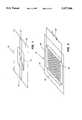
- FIG. 1is a schematic prospective view of an elementary surface cell device of the invention.
- FIG. 2is a schematic perspective view of another embodiment of the device of this invention.
- FIG. 3is a schematic representation of a process used to prepare the devices of this invention.
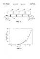
- FIG. 4 and FIG. 5are graphs of luminescence vs voltage for the present devices.
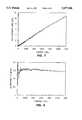
- FIG. 6is a current vs voltage curve for a device of this invention.
- FIG. 7is a graph of emitted light intensity as a function of current for a surface cell device.
- FIG. 8is a graph of electroluminescent efficiency as a function of current for such a device.
- FIG. 9is a graph of electroluminescence intensities collected in front of and in back of a device with a transparent substrate as a function of drive current.
- FIG. 10is a graph showing the good shelf-life achieved with the devices of this invention.
- a surface cell configurationcan be envisioned for thin film EL devices with numerous advantages.
- electrodesmay be pre-prepared onto a substrate with a gap in between them.
- FIG. 1a simple surface cell configuration is shown in FIG. 1.
- Device 10includes anode 12 and cathode 14 in contact with semiconducting electroluminescent and ionic layer 16 (preferably made of a conducting polymer) carried by substrate 18.
- Substrate 18may be flexible plastic if desired and also is often transparent.
- the metal electrodes 12 and 14can be fabricated on the substrate 18 by, for example, thermal evaporation, electron beam evaporation, sputtering, chemical deposition, printing and so on.
- the electrodescan be patterned. This can be done either with a shadow mask or by means of photolithographic techniques well known in the art.
- the electrodes 12 and 14can be fabricated in an interdigitated pattern as shown in b of FIG. 2 where they are shown coupled to switched power supply 20.
- This interdigitated electrode configurationhas been used in polymer field effect transistors to increase the source-to-drain current density for a given gate electrode area for example, A. Assadi, C. Svensson, M. Wilander and 0. Inganas, Appl. Phys. Lett. 53 (1988) 195; F. Garnier, G. Horowitz, X. Peng and D. Fichou, Adv. Mater. 2 (1990) 592!.
- the interdigitated surface cell electrode configurationhas not been used in thin film electroluminescent devices heretofore for a number of reasons.
- Conventional organic or inorganic semiconducting materialshave high bulk resistivities; thus requiring sub-micron dimensions. Different metals are required as the carrier-injecting electrodes.
- the thin film organic EL devicesrequire high electric fields for carrier injection I. D. Parker, J. Appl. Phys. 75 (1994) 1656!, the use of a surface cell configuration might be considered to require dangerously high voltage operation. For example, a polymer light-emitting diode which turns on at 5 volts in sandwich cell with film thickness of 1000 ⁇ would require approximately 250 volts in a surface cell with interdigitated electrode spacing of 5 ⁇ m.
- the thickness and the film qualities (surface roughness, pinholes etc.) of the luminescent semiconducting materialare not critical in the surface cell configuration.
- light-emitting electrochemical cell devicesare fabricated in a single step by depositing the semiconducting luminescent material (for example by casting from solution) onto pre-patterned electrodes with no need for subsequent deposition of electrodes after casting the polymer film.
- the surface cell configurationoffers significant manufacturing advantages over the prior art.
- the inventionprovides a device configuration such as shown in FIGS. 1 and 2 for implementation of the light-emitting electrochemical cell in a surface cell configuration and a method of obtaining light from said surface light-emitting electrochemical cell.
- the electrodesare interdigitated metal electrodes patterned on the substrate by vacuum deposition through a shadow mask.
- the interdigitated electrodesare patterned onto the substrate using photolithography.
- photolithographic methodsis particularly important when high resolution is required.
- the interdigitated electrodesare patterned onto the substrate using the methods of screen printing.
- interdigitated electrodesneed not be in the form of straight line patterns.
- interdigitated spiral patternscan be utilized to obtain an overall shape that is circular or oval.
- the light-emitting areacan be patterned into a wide range of unusual, useful and appealing patterns.
- interdigitated electrodesneed not be patterned in a symmetric fashion.
- interdigitated electrodescan be patterned with closely spaced pairs separated from other closely spaced pairs by a larger distance. In this way, overall light emission intensity can be controlled by the electrode geometry since on the fraction of the total area which is between the closely spaced pairs will be bright. This means that light-emitting cells can be designed and fabricated to operate at a specific optimum voltage (for example, highest efficiency, longest lifetime, etc.) with different brightness or different patterns of brightness.
- a preferred embodimentutilizes transparent substrates, for example, glass or plastic, so that the light emitted from the surface light-emitting electrochemical cell can be seen from either side.
- Such surface light-emitting electrochemical cellsenable a new type of flat light source which can be viewed from both sides.
- the substrateis a flexible transparent plastic.
- Such surface light-emitting electrochemical cellsenable a new type of flat panel display which can be made with plastic materials such that they have a thin profile and such that they are fully flexible.
- the active medium of a polymer light-emitting electrochemical cellis a blend of a semiconducting and luminescent polymer containing a sufficient density of ionic species (i.e. with sufficient salt) as additive to provide the counterions necessary for p-type and n-type doping.
- a semiconducting and luminescent polymercontaining a sufficient density of ionic species (i.e. with sufficient salt) as additive to provide the counterions necessary for p-type and n-type doping.
- an ionically conductive materialis required. That ionically conducting material can be the semiconducting and luminescent polymer, possibly enhanced by blending with a known ion transport polymer (for example, polyethylene-oxide, "PEO").
- this blendis deposited onto a substrate; said substrate having a pre-patterned array of interdigitated electrodes on its surface. Light is emitted between the electrode pairs.
- the polymer solid state light-emitting electrochemical cellis based on the following operating principles:
- the electrolyte(ion pairs plus ionically conductive material) is initially distributed uniformly throughout the active medium, such that the medium has ionic conductivity ⁇ 10 -8 S/cm;
- the fluorescent speciesis also distributed uniformly and must be capable of both p-type and n-type doping;
- the doping profileis dynamically changed in a controlled fashion through reversible electrochemical oxidation and reduction to form a p-type layer on one side, an n-type layer on the opposite side, and a p-n junction at the interface between the two.
- Light emissionis from the compensated region within the p-n junction.
- the devicescomprise pre-patterned metal contacts in surface configurations (such as, for example, that shown in FIGS. 1 and 2) on flat or curved substrates on either rigid or flexible substrates.
- a variety of substratescan be used, for example either plastic or glass, with plastic substrates offering the particular advantage of device flexibility. Because of the surface cell configuration, the substrate need not be transparent; thus allowing a wide range of substrates, including, for example, semiconductors, ceramics, and metals. Metallic substrates require an insulating layer between the substrate and the surface cell. Such an insulating layer can be patterned such that one of the interdigitated electrodes can be the metal substrate.
- a principal advantage obtained with the use of transparent substratesis that the light emitted from the surface cell light-emitting electrochemical cell can be seem from either side.
- Such surface light-emitting electrochemical cellstherefore enable a new type of flat light source which can be viewed from both sides and which can be made with plastic materials such that they have a thin profile and such that they are fully flexible.
- the electrodesare interdigitated metal electrodes patterned on the substrate.
- the interdigitated electrode patterncan be fabricated by a variety of methods; for example, by vacuum deposition through a shadow mask, by screen printing, or by using the methods of photolithography, or by the use of a variety of other methods known in the art.
- the use of photolithographic methodsis particularly important when high spatial resolution is required.
- the electrodescan be patterned by laser ablation of a thin film conducting layer (metal or doped conducting polymer).
- the electrodescan be patterned by UV degradation; for example conducting polyaniline can be converted into an insulator by exposure to intense UV radiation.
- the interdigitated electrodesneed not be in the form of straight line patterns.
- interdigitated spiral patternscan be utilized to obtain an overall shape that is circular or oval.
- the light-emitting areacan be patterned into a wide range of unusual, useful and appealing patterns.
- the interdigitated electrodesneed not be patterned in a symmetric fashion.
- interdigitated electrodescan be patterned with closely spaced pairs separated from other closely spaced pairs by a larger distance. In this way, overall light emission intensity can be controlled by the electrode geometry; for example only a fraction of the total area can be used and the device designed and fabricated to operate at a specific optimum voltage (for example, highest efficiency, longest lifetime etc.) with different brightness or different patterns of brightness.
- the metallic material to be used for the interdigitated electrodescan be conventional metals (such as Au, Cu or Al), conducting polymers such as, for example, polyaniline in the conducting emeralding salt form, conducting oxides such as indium/tin oxide, etc., the principal requirement being that said electrode materials form good electrical contact to the medium between them, and remain inert in the electrochemical doping reactions.
- the metals which form the interdigitated electrodescan be the same or they can be different. The use of identical, stable electrode materials is preferred to facilitate the fabrication of the interdigitated pattern.
- the semiconducting, luminescent and ionically conducting materialwhich comprises the active light-emitting region between the electrodes is described in detail in U.S. patent application Ser. No. 08/268,763 which is incorporated by reference.
- the active materialcan be deposited between the electrodes in the surface cell configuration by a variety of convenient and well-known methods, including casting from solution, dip-coating the pre-patterned substrate into a solution containing the active material, vapor deposition, etc.
- Film thicknesses for the active semiconducting, luminescent and ionically conducting materialare not critical and range from a few hundred Angstrom units to a few microns, or even thicker. A limitation on the thickness is set by the transparency of the active material at the wavelength of emission. For efficient external generation of light the film thickness should be such that the optical density at the emission wavelength is less than unity (OD ⁇ 1).
- the deviceFor devices used for viewing in both front and back directions, it is desirable that the device be semi-transparent throughout the visible spectrum.
- film thicknessesshould be limited such that the optical density (OD) at the absorption peak ⁇ 3; typically less than 6000 ⁇ for most conjugated polymers.
- ODoptical density
- blue-emitting devices with low absorption throughout the visible spectrumtransparency does not limit the thickness.
- Electrodes or matrices of such devicescan be fabricated by electrode patterning. Relatively large sizes can be fabricated with, for example, many units repeated on a single sheet or with a single complex pattern extending over a relatively large area.
- a continuous manufacturing process(using linear coating technology for the semiconducting, luminescent and ionically transporting material) can be envisioned in a "roll to roll" process as shown schematically in FIG. 3.
- a device of this inventioncan be continuously prepared by passing a sheet of flexible substrate 18 from feed spool 22 to take-up spool 24.
- a layer of conductive electrode-forming materialis deposited.
- this layeris patterned with U.V. light to give use to a pattern of interdigitated electrodes.
- a layer of electroluminescent materialin deposited onto the interdigitated electrodes.
- an optional protective overlayeris applied.
- the continuous sheetis cut into individual devices.
- LEC cell deviceswere fabricated by drop casting an active blend of semiconducting luminescent polymer (MEH-PPV) and ionic species source from solution onto a substrate with interdigitated gold electrodes fabricated by photolithographic methods.
- the preparation of the active blendhas been described in detail in U.S. patent application Ser. No. 08/268,763.
- the gap size between the interstitial electrodeswas 5 ⁇ m.; the total device size was 5 mm ⁇ 5 mm (see FIG. 2).
- the equivalent length (L) to width (W) ratio (L/W)is 5 ⁇ 10 5 . These values are exemplary. Typical gap widths are from about 1 ⁇ m to about 100 ⁇ m and preferably 1.5 ⁇ m to 50 ⁇ m and especially 2 ⁇ m to 40 ⁇ m. Electrode widths can be similar widths although wider electrodes can also be used.
- FIG. 4shows the luminance as a function of bias voltage for a 5 ⁇ m gap device. Light was detected for V ⁇ 5 V. The emitted light reached an intensity of approximately 100 cd/m 2 at -15 V. The color of the emitted light was characteristic of the emission from MEH-PPV and was similar to that observed in light-emitting electrochemical cell devices fabricated in the sandwich cell configuration.
- This exampledemonstrates low-voltage light emission from the light-emitting electrochemical cell in the surface cell configuration. Radiative recombination of the injected carriers occurs in the semiconducting, luminescent and ionically conducting blend; said radiation originating from the conjugated polymer as the luminescent medium.
- the turn-on voltagewas somewhat greater than the energy gap of the luminescent polymer (the turn on was approximately 3 V, see FIG. 5; the energy gap of MEH-PPV is approx. 2.1 V).
- the operating voltagecan be further reduced by fabricating polymer blend materials with higher ionic conductivity and/or by utilizing interdigitated electrodes with narrower inter-electrode spacing.
- Electrode deviceswere fabricated by drop casting the active blend from solution onto a glass substrate with interdigitated gold electrodes fabricated by photolithographic methods.
- the gap size between the interdigitated electrodeswas 30 ⁇ m and the width of the individual electrodes was 10 ⁇ m.
- the total equivalent length of the electrodeis 22.5 cm.
- the L/W rationis 550.
- the lateral dimensions of the devicewere 3 mm ⁇ 3 mm; i.e. with a total area of 0.09 cm 2 .
- the thickness of the drop cast film used in this examplewas greater than one micron.
- FIG. 6A typical current(I) vs voltage (V), I-V dependence obtained from a 30 ⁇ m gap device is shown in FIG. 6. This asymmetric I-V curve (solid dots) was recorded after biasing the device in a given polarity for about one minute. The rectification ration is >100 at 90 V, corresponding to a field strength of 3 ⁇ 10 4 V/cm. In contrast, the common field strength used for polymer LEDs in the sandwich configuration is ⁇ 10 6 V/cm.
- This rectifying diode characteristicwas erased by applying an alternating field with gradually-attenuated magnitude.
- the devicewas switched into the opposite direction by first applying the external field in the reverse direction.
- Also plotted in FIG. 6is the I-V characteristic of the same device after applying field in reverse direction (open dots) for ⁇ 5 minutes. Nearly identical rectifying behavior is created in the opposite direction.
- the switching timecan be reduced significantly with reduced gap size or with blends of higher ionic mobility.
- This exampledemonstrates that a rectifying diode can be generated in-situ and that said diode behavior can be erased in the surface configuration electrochemical cell with the application of external bias; i.e., the in-situ electrochemical doping results in the formation of a dynamic p-n junction within the polymer blend.
- This rectifying diodecan be switched to the opposite direction with reversed bias.
- Electrode deviceswere fabricated by drop casting the active blend from solution onto a substrate with interdigitated gold electrodes fabricated by photolithographic methods.
- the gap size between the interstitial electrodeswas 30 ⁇ m and the width of the individual electrodes was 10 ⁇ m, as described in detail in Example 2.
- the emitted light intensitywas proportional to the injected current as demonstrated in FIG. 7.
- the EL efficiency of this devicewas measured to be ⁇ 0.3% photons/electron, as shown in FIG. 8. These data were collated only from light emitted from the front of the device.
- the EL efficiency in reference light emitting electrochemical cells in the sandwich configuration fabricated with the same LEEC blendswas ⁇ 0.5-0.7% ph/el (with the blend thickness of ⁇ 1500 ⁇ ).
- the total EL efficiency in the surface cellwas similar to that in sandwich cell device.
- Light-emitting electrochemical cellswere fabricated in the surface cell configuration (30 ⁇ m gap) utilizing transparent substrates. Light was emitted and observed from both front and back directions. The EL intensities collected in both front and back directions are plotted as a function of the drive current in FIG. 9.
- This exampledemonstrates a novel feature of the surface cell configuration; the emitted light can be viewed from both the front and the back side of the display; an obvious advantage for display applications.
- the shelf life of the surface EL cellswas monitored for a period in excess of eight months.
- the device used in this Examplewas a 30 ⁇ m gap surface cell; the device was stored in a controlled atmosphere (Argon) dry box during the entire test period.
- the EL efficiencyremains at the level of 0.3% ph/el during the entire period; no degradation of EL efficiency was observed.
- Black spot formationhas become one of the key issues limiting the shelf life of conventional organic and polymer LEDs. This black spot formation is associated with deterioration of the cathode/polymer interface. Since the light-emitting electrochemical cell is fabricated with the semiconductor polymer in its neutral form, since stable metals are used for the contacting electrodes, and since the electrochemically induced p-n junction is generated in-situ, all components are environmentally stable in the quiescent "off" state. As a result, light-emitting electrochemical cells exhibit intrinsically longer shelf life when compared to conventional polymer light-emitting diodes. Indeed, light-emitting electrochemical cells in the surface cell configuration, fabricated with either Au or PANI electrodes, showed no black spots after storage for 8 months.
Landscapes
- Physics & Mathematics (AREA)
- Optics & Photonics (AREA)
- Electroluminescent Light Sources (AREA)
Abstract
Description
Claims (24)
Priority Applications (4)
| Application Number | Priority Date | Filing Date | Title |
|---|---|---|---|
| US08/444,998US5677546A (en) | 1995-05-19 | 1995-05-19 | Polymer light-emitting electrochemical cells in surface cell configuration |
| EP96914717AEP0826248A4 (en) | 1995-05-19 | 1996-05-20 | ELECTROCHEMICAL LIGHT-EMITTING DEVICES |
| AU57995/96AAU5799596A (en) | 1995-05-19 | 1996-05-20 | Electrochemical light-emitting devices |
| PCT/US1996/007257WO1996037001A1 (en) | 1995-05-19 | 1996-05-20 | Electrochemical light-emitting devices |
Applications Claiming Priority (1)
| Application Number | Priority Date | Filing Date | Title |
|---|---|---|---|
| US08/444,998US5677546A (en) | 1995-05-19 | 1995-05-19 | Polymer light-emitting electrochemical cells in surface cell configuration |
Publications (1)
| Publication Number | Publication Date |
|---|---|
| US5677546Atrue US5677546A (en) | 1997-10-14 |
Family
ID=23767241
Family Applications (1)
| Application Number | Title | Priority Date | Filing Date |
|---|---|---|---|
| US08/444,998Expired - LifetimeUS5677546A (en) | 1995-05-19 | 1995-05-19 | Polymer light-emitting electrochemical cells in surface cell configuration |
Country Status (1)
| Country | Link |
|---|---|
| US (1) | US5677546A (en) |
Cited By (54)
| Publication number | Priority date | Publication date | Assignee | Title |
|---|---|---|---|---|
| US5966393A (en)* | 1996-12-13 | 1999-10-12 | The Regents Of The University Of California | Hybrid light-emitting sources for efficient and cost effective white lighting and for full-color applications |
| US6008828A (en)* | 1995-11-06 | 1999-12-28 | Fuji Xerox Co., Ltd. | Image forming apparatus including conducting polymer layer for ionic dye intake and release |
| US6099980A (en)* | 1996-07-16 | 2000-08-08 | U.S. Philips Corporation | Organic electroluminescent device |
| WO2001006577A1 (en)* | 1999-07-20 | 2001-01-25 | Sri International | Cavity-emission electroluminescent device and method for forming the device |
| DE19935823A1 (en)* | 1999-07-29 | 2001-03-01 | Infineon Technologies Ag | Electro-optical microelectronic arrangement used as a transistor, diode or capacitor comprises a metallizing plane on an integrated semiconductor circuit system |
| US6455873B1 (en)* | 1997-12-03 | 2002-09-24 | State Of Oregon Acting By And Through The State Board Of Higher Education On Behalf Of The University Of Oregon | Devices having a semiconductor/conducting polymer interface |
| US20020180670A1 (en)* | 2001-05-04 | 2002-12-05 | Lg Electronics Inc. | Scan structure in display device, method for driving the display device, and method for manufacturing the same |
| WO2002061837A3 (en)* | 2001-01-31 | 2003-02-20 | Seiko Epson Corp | Modular display device and organic thin-film transistor |
| US6548836B1 (en) | 1999-04-29 | 2003-04-15 | Massachusetts Institute Of Technology | Solid state light-emitting device |
| US20030127967A1 (en)* | 2001-12-05 | 2003-07-10 | Semiconductor Energy Laboratory Co., Ltd. | Organic semiconductor element |
| US20030183830A1 (en)* | 2002-01-24 | 2003-10-02 | Semiconductor Energy Laboratory Co., Ltd. | Light emitting device, method of preparing the same and device for fabricating the same |
| US6630793B2 (en) | 2000-08-16 | 2003-10-07 | Massachusetts Institute Of Technology | High efficiency solid state light-emitting device and method of generating light |
| US20030218173A1 (en)* | 2002-04-09 | 2003-11-27 | Takeshi Nishi | Light emitting device |
| US20040027059A1 (en)* | 2002-08-09 | 2004-02-12 | Semiconductor Energy Laboratory Co., Ltd. | Organic electroluminescent device |
| US20040027061A1 (en)* | 2002-08-09 | 2004-02-12 | Semiconductor Energy Laboratory Co., Ltd. | Electroluminescence element and a light emitting device using the same |
| US6696096B2 (en)* | 2000-06-22 | 2004-02-24 | Matsushita Electric Works, Ltd. | Apparatus for and method of vacuum vapor deposition and organic electroluminescent device |
| US20040041519A1 (en)* | 2002-08-30 | 2004-03-04 | Tomy Company, Ltd. | Electroluminescence light emitting display system |
| US20040041755A1 (en)* | 2002-08-30 | 2004-03-04 | Tomy Company, Ltd. | Electroluminescence light emitting display system and electroluminescence light emitting sheet |
| US20040041517A1 (en)* | 2002-08-30 | 2004-03-04 | Tomy Company, Ltd. | Electroluminescence light emitting display system and electroluminescence light emitting sheet |
| US20040104671A1 (en)* | 2002-08-30 | 2004-06-03 | Tomy Company, Ltd. | Electroluminescence light emitting device and method for manufacturing the same |
| US20040113541A1 (en)* | 2002-08-30 | 2004-06-17 | Tomy Company, Ltd. | Electroluminescence light emitting sheet |
| US20040135160A1 (en)* | 2003-01-10 | 2004-07-15 | Eastman Kodak Company | OLED device |
| US20040150333A1 (en)* | 2002-08-09 | 2004-08-05 | Semiconductor Energy Laboratory Co., Ltd. | Organic electroluminescent device |
| DE10314163A1 (en)* | 2003-03-28 | 2004-10-28 | Siemens Ag | Electro-optical thin-film microwave detector |
| US6836068B2 (en)* | 2001-04-27 | 2004-12-28 | Canon Kabushiki Kaisha | Organic electroluminescent device and display apparatus |
| US20050023137A1 (en)* | 2003-06-20 | 2005-02-03 | Bhullar Raghbir S. | Biosensor with multiple electrical functionalities |
| US20050045917A1 (en)* | 2001-12-28 | 2005-03-03 | Semiconductor Energy Laboratory Co., Ltd. | Light emitting device, method of manufacturing the same and manufacturing apparatus therefor |
| US20050069726A1 (en)* | 2003-09-30 | 2005-03-31 | Douglas Elliot Paul | Light emitting composite material and devices thereof |
| US20050134173A1 (en)* | 2003-08-25 | 2005-06-23 | Tetsuo Tsutsui | Electrode device for organic device and electronic device having the same |
| US20050152125A1 (en)* | 2002-05-17 | 2005-07-14 | Shinsaku Fukuda | El light emitting device |
| US20060011461A1 (en)* | 1998-11-13 | 2006-01-19 | Chan Sam E J | Computer keyboard backlighting |
| US7109661B2 (en) | 2002-08-30 | 2006-09-19 | Tomy Company, Ltd. | Electroluminescence light emitting display system |
| US7199521B2 (en) | 2003-01-29 | 2007-04-03 | Semiconductor Energy Laboratory Co., Ltd. | Electroluminescence device |
| US20070082227A1 (en)* | 2005-09-29 | 2007-04-12 | Tsuyoshi Kobayashi | Light-emitting device |
| US20070090758A1 (en)* | 2005-10-21 | 2007-04-26 | Kwasny David M | Electroluminescent panel |
| US20080007936A1 (en)* | 2006-07-05 | 2008-01-10 | Jie Liu | Organic illumination source and method for controlled illumination |
| US20080017870A1 (en)* | 2006-04-04 | 2008-01-24 | Georg Diamantidis | Semiconductor light-emitting means and light-emitting panel comprising the same |
| WO2008060348A1 (en) | 2006-11-14 | 2008-05-22 | Sri International | Cavity electroluminescent devices and methods for producing the same |
| US20080212307A1 (en)* | 1998-11-13 | 2008-09-04 | Chan Sam E J | Computer keyboard backlighting |
| US20090092855A1 (en)* | 2005-08-23 | 2009-04-09 | University Of Cape Town | Doping of particulate semiconductor materials |
| US20090091478A1 (en)* | 1998-11-13 | 2009-04-09 | Chan Sam E J | Computer keyboard backlighting |
| US20090121609A1 (en)* | 2007-10-29 | 2009-05-14 | Dai Nippon Printing Co., Ltd. | Liquid light-emitting element, light-emitting device, method for making light-emitting device, and light-emitting body |
| US20090151864A1 (en)* | 2003-06-20 | 2009-06-18 | Burke David W | Reagent stripe for test strip |
| US20090179196A1 (en)* | 2006-03-20 | 2009-07-16 | Chihaya Adachi | Pyrene-Based Organic Compound, Transistor Material and Light-Emitting Transistor Device |
| US20100302532A1 (en)* | 2007-03-29 | 2010-12-02 | Avago Technologies Ecbu Ip (Singapore) Pte. Ltd. | Photodetector having dark current correction |
| US20110042657A1 (en)* | 2008-01-24 | 2011-02-24 | Yijian Shi | High Efficiency Electroluminescent Devices and Methods for Producing the Same |
| WO2011053236A1 (en) | 2009-10-28 | 2011-05-05 | Lunavation Ab | A light-emitting electrochemical device, a system comprising such a device and use of such a device |
| US8071030B2 (en) | 2003-06-20 | 2011-12-06 | Roche Diagnostics Operations, Inc. | Test strip with flared sample receiving chamber |
| US8080934B2 (en) | 2002-03-26 | 2011-12-20 | Rohm Company, Ltd. | Organic electroluminescent device having an electrically insulating charge generation layer |
| US8148164B2 (en) | 2003-06-20 | 2012-04-03 | Roche Diagnostics Operations, Inc. | System and method for determining the concentration of an analyte in a sample fluid |
| US8183559B2 (en) | 2002-05-21 | 2012-05-22 | Semiconductor Energy Laboratory Co., Ltd. | Organic field effect transistor |
| US8679853B2 (en) | 2003-06-20 | 2014-03-25 | Roche Diagnostics Operations, Inc. | Biosensor with laser-sealed capillary space and method of making |
| CN103858248A (en)* | 2011-08-02 | 2014-06-11 | 住友化学株式会社 | dopant injection layer |
| US10115915B1 (en)* | 2017-04-28 | 2018-10-30 | Tsinghua University | Organic thin film transistor and method for making the same |
Citations (11)
| Publication number | Priority date | Publication date | Assignee | Title |
|---|---|---|---|---|
| US3404304A (en)* | 1964-04-30 | 1968-10-01 | Texas Instruments Inc | Semiconductor junction device for generating optical radiation |
| US3701043A (en)* | 1970-02-16 | 1972-10-24 | Mc Donnell Douglas Corp | Negative resistance light emitting diode device |
| US3900418A (en)* | 1973-04-12 | 1975-08-19 | Bell Northern Research Ltd | Electrochemical luminescent solutions and devices incorporating such solutions |
| JPS59188181A (en)* | 1984-03-23 | 1984-10-25 | Hitachi Ltd | silicon vice mount |
| US4539507A (en)* | 1983-03-25 | 1985-09-03 | Eastman Kodak Company | Organic electroluminescent devices having improved power conversion efficiencies |
| US5155566A (en)* | 1990-03-27 | 1992-10-13 | Kabushiki Kaisha Toshiba | Organic thin film element |
| US5189549A (en)* | 1990-02-26 | 1993-02-23 | Molecular Displays, Inc. | Electrochromic, electroluminescent and electrochemiluminescent displays |
| US5247190A (en)* | 1989-04-20 | 1993-09-21 | Cambridge Research And Innovation Limited | Electroluminescent devices |
| US5250820A (en)* | 1991-01-30 | 1993-10-05 | Rohm Co., Ltd. | Light emitting diode having uniform light distribution |
| US5258629A (en)* | 1991-05-14 | 1993-11-02 | Eastman Kodak Company | Light-emitting diode print head with staggered electrodes |
| US5408109A (en)* | 1991-02-27 | 1995-04-18 | The Regents Of The University Of California | Visible light emitting diodes fabricated from soluble semiconducting polymers |
- 1995
- 1995-05-19USUS08/444,998patent/US5677546A/ennot_activeExpired - Lifetime
Patent Citations (11)
| Publication number | Priority date | Publication date | Assignee | Title |
|---|---|---|---|---|
| US3404304A (en)* | 1964-04-30 | 1968-10-01 | Texas Instruments Inc | Semiconductor junction device for generating optical radiation |
| US3701043A (en)* | 1970-02-16 | 1972-10-24 | Mc Donnell Douglas Corp | Negative resistance light emitting diode device |
| US3900418A (en)* | 1973-04-12 | 1975-08-19 | Bell Northern Research Ltd | Electrochemical luminescent solutions and devices incorporating such solutions |
| US4539507A (en)* | 1983-03-25 | 1985-09-03 | Eastman Kodak Company | Organic electroluminescent devices having improved power conversion efficiencies |
| JPS59188181A (en)* | 1984-03-23 | 1984-10-25 | Hitachi Ltd | silicon vice mount |
| US5247190A (en)* | 1989-04-20 | 1993-09-21 | Cambridge Research And Innovation Limited | Electroluminescent devices |
| US5189549A (en)* | 1990-02-26 | 1993-02-23 | Molecular Displays, Inc. | Electrochromic, electroluminescent and electrochemiluminescent displays |
| US5155566A (en)* | 1990-03-27 | 1992-10-13 | Kabushiki Kaisha Toshiba | Organic thin film element |
| US5250820A (en)* | 1991-01-30 | 1993-10-05 | Rohm Co., Ltd. | Light emitting diode having uniform light distribution |
| US5408109A (en)* | 1991-02-27 | 1995-04-18 | The Regents Of The University Of California | Visible light emitting diodes fabricated from soluble semiconducting polymers |
| US5258629A (en)* | 1991-05-14 | 1993-11-02 | Eastman Kodak Company | Light-emitting diode print head with staggered electrodes |
Cited By (134)
| Publication number | Priority date | Publication date | Assignee | Title |
|---|---|---|---|---|
| US6008828A (en)* | 1995-11-06 | 1999-12-28 | Fuji Xerox Co., Ltd. | Image forming apparatus including conducting polymer layer for ionic dye intake and release |
| US6099980A (en)* | 1996-07-16 | 2000-08-08 | U.S. Philips Corporation | Organic electroluminescent device |
| US5966393A (en)* | 1996-12-13 | 1999-10-12 | The Regents Of The University Of California | Hybrid light-emitting sources for efficient and cost effective white lighting and for full-color applications |
| US6455873B1 (en)* | 1997-12-03 | 2002-09-24 | State Of Oregon Acting By And Through The State Board Of Higher Education On Behalf Of The University Of Oregon | Devices having a semiconductor/conducting polymer interface |
| US20080212307A1 (en)* | 1998-11-13 | 2008-09-04 | Chan Sam E J | Computer keyboard backlighting |
| US20060011461A1 (en)* | 1998-11-13 | 2006-01-19 | Chan Sam E J | Computer keyboard backlighting |
| US20090091478A1 (en)* | 1998-11-13 | 2009-04-09 | Chan Sam E J | Computer keyboard backlighting |
| US7335843B2 (en)* | 1998-11-13 | 2008-02-26 | Firefly International, Inc. | Computer keyboard backlighting |
| US6548836B1 (en) | 1999-04-29 | 2003-04-15 | Massachusetts Institute Of Technology | Solid state light-emitting device |
| WO2001006577A1 (en)* | 1999-07-20 | 2001-01-25 | Sri International | Cavity-emission electroluminescent device and method for forming the device |
| US6593687B1 (en) | 1999-07-20 | 2003-07-15 | Sri International | Cavity-emission electroluminescent device and method for forming the device |
| DE19935823A1 (en)* | 1999-07-29 | 2001-03-01 | Infineon Technologies Ag | Electro-optical microelectronic arrangement used as a transistor, diode or capacitor comprises a metallizing plane on an integrated semiconductor circuit system |
| DE19935823B4 (en)* | 1999-07-29 | 2006-07-13 | Infineon Technologies Ag | Electro-optical microelectronic assembly and method for its production |
| US6696096B2 (en)* | 2000-06-22 | 2004-02-24 | Matsushita Electric Works, Ltd. | Apparatus for and method of vacuum vapor deposition and organic electroluminescent device |
| US6630793B2 (en) | 2000-08-16 | 2003-10-07 | Massachusetts Institute Of Technology | High efficiency solid state light-emitting device and method of generating light |
| US7068418B2 (en) | 2001-01-31 | 2006-06-27 | Seiko Epson Corporation | Display device |
| US7468580B2 (en) | 2001-01-31 | 2008-12-23 | Seiko Epson Corporation | Display device |
| US20080246704A1 (en)* | 2001-01-31 | 2008-10-09 | Seiko Epson Corporation | Display device |
| US20030141807A1 (en)* | 2001-01-31 | 2003-07-31 | Takeo Kawase | Display device |
| WO2002061837A3 (en)* | 2001-01-31 | 2003-02-20 | Seiko Epson Corp | Modular display device and organic thin-film transistor |
| US20050218791A1 (en)* | 2001-01-31 | 2005-10-06 | Seiko Epson Corporation | Display device |
| US8139005B2 (en) | 2001-01-31 | 2012-03-20 | Seiko Epson Corporation | Display device |
| US6836068B2 (en)* | 2001-04-27 | 2004-12-28 | Canon Kabushiki Kaisha | Organic electroluminescent device and display apparatus |
| US7015638B2 (en) | 2001-04-27 | 2006-03-21 | Canon Kabushiki Kaisha | Organic electroluminescent device and display apparatus |
| US7068265B2 (en) | 2001-05-04 | 2006-06-27 | Lg Electronics Inc. | Scan structure in display device, method for driving the display device, and method for manufacturing the same |
| EP1260958A3 (en)* | 2001-05-04 | 2004-06-09 | LG Electronics, Inc. | Scan structure in display device, method for driving the display device, and method for manufacturing the same |
| US20020180670A1 (en)* | 2001-05-04 | 2002-12-05 | Lg Electronics Inc. | Scan structure in display device, method for driving the display device, and method for manufacturing the same |
| US11217764B2 (en) | 2001-12-05 | 2022-01-04 | Semiconductor Energy Laboratory Co., Ltd. | Organic semiconductor element |
| US20060091797A1 (en)* | 2001-12-05 | 2006-05-04 | Semiconductor Energy Laboratory Co., Ltd. | Organic semiconductor element |
| US7420203B2 (en) | 2001-12-05 | 2008-09-02 | Semiconductor Energy Laboratory Co., Ltd. | Organic semiconductor element |
| US20030127967A1 (en)* | 2001-12-05 | 2003-07-10 | Semiconductor Energy Laboratory Co., Ltd. | Organic semiconductor element |
| US7956349B2 (en)* | 2001-12-05 | 2011-06-07 | Semiconductor Energy Laboratory Co., Ltd. | Organic semiconductor element |
| US7956353B2 (en) | 2001-12-05 | 2011-06-07 | Semiconductor Energy Laboratory Co., Ltd. | Organic semiconductor element |
| US7473923B2 (en) | 2001-12-05 | 2009-01-06 | Semiconductor Energy Laboratory Co., Ltd. | Organic semiconductor element |
| US9312507B2 (en) | 2001-12-05 | 2016-04-12 | Semiconductor Energy Laboratory Co., Ltd. | Organic semiconductor element |
| US20090045738A1 (en)* | 2001-12-05 | 2009-02-19 | Semiconductor Energy Laboratory Co., Ltd. | Organic Semiconductor Element |
| US8941096B2 (en) | 2001-12-05 | 2015-01-27 | Semiconductor Energy Laboratory Co., Ltd. | Organic semiconductor element |
| US20110227119A1 (en)* | 2001-12-05 | 2011-09-22 | Semiconductor Energy Laboratory Co., Ltd. | Organic Semiconductor Element |
| US7057209B2 (en) | 2001-12-28 | 2006-06-06 | Semiconductor Energy Laboratory Co., Ltd. | Light emitting device, method of manufacturing the same and manufacturing apparatus therefor |
| US10497755B2 (en) | 2001-12-28 | 2019-12-03 | Semiconductor Energy Laboratory Co., Ltd. | Light emitting device, method of manufacturing the same, and manufacturing apparatus therefor |
| US9048203B2 (en) | 2001-12-28 | 2015-06-02 | Semiconductor Energy Laboratory Co., Ltd. | Light emitting device, method of manufacturing the same, and manufacturing apparatus therefor |
| US7982206B2 (en) | 2001-12-28 | 2011-07-19 | Semiconductor Energy Laboratory Co., Ltd. | Light emitting device, method of manufacturing the same, and manufacturing apparatus therefor |
| US7719014B2 (en) | 2001-12-28 | 2010-05-18 | Semiconductor Energy Laboratory Co., Ltd. | Light emitting device, method of manufacturing the same, and manufacturing apparatus therefor |
| US9450030B2 (en) | 2001-12-28 | 2016-09-20 | Semiconductor Energy Laboratory Co., Ltd. | Active matrix light-emitting device with overlapping electroluminescent layers |
| US7420210B2 (en) | 2001-12-28 | 2008-09-02 | Semiconductor Energy Laboratory Co., Ltd. | Light emitting device, method of manufacturing the same, and manufacturing apparatus therefor |
| US20050045917A1 (en)* | 2001-12-28 | 2005-03-03 | Semiconductor Energy Laboratory Co., Ltd. | Light emitting device, method of manufacturing the same and manufacturing apparatus therefor |
| US20090008643A1 (en)* | 2001-12-28 | 2009-01-08 | Semiconductor Energy Laboratory Co., Ltd. | Light Emitting Device, Method of Manufacturing the Same, and Manufacturing Apparatus Therefor |
| US20100295052A1 (en)* | 2001-12-28 | 2010-11-25 | Semiconductor Energy Laboratory Co., Ltd. | Light Emitting Device, Method of Manufacturing the Same, and Manufacturing Apparatus Therefor |
| US20060208263A1 (en)* | 2001-12-28 | 2006-09-21 | Semiconductor Energy Laboratory Co., Ltd. | Light emitting device, method of manufacturing the same, and manufacturing apparatus therefor |
| US9236418B2 (en) | 2002-01-24 | 2016-01-12 | Semiconductor Energy Laboratory Co., Ltd. | Light emitting device |
| US20030183830A1 (en)* | 2002-01-24 | 2003-10-02 | Semiconductor Energy Laboratory Co., Ltd. | Light emitting device, method of preparing the same and device for fabricating the same |
| US7098069B2 (en) | 2002-01-24 | 2006-08-29 | Semiconductor Energy Laboratory Co., Ltd. | Light emitting device, method of preparing the same and device for fabricating the same |
| US9653519B2 (en) | 2002-01-24 | 2017-05-16 | Semiconductor Energy Laboratory Co., Ltd. | Light emitting device, method of preparing the same and device for fabricating the same |
| US8629439B2 (en) | 2002-01-24 | 2014-01-14 | Semiconductor Energy Laboratory Co., Ltd. | Light emitting device, method of preparing the same and device for fabricating the same |
| US8080934B2 (en) | 2002-03-26 | 2011-12-20 | Rohm Company, Ltd. | Organic electroluminescent device having an electrically insulating charge generation layer |
| US10998527B2 (en) | 2002-03-26 | 2021-05-04 | Rohm Co., Ltd. | Organic electroluminescent device |
| US10319949B2 (en) | 2002-03-26 | 2019-06-11 | Rohm Co., Ltd. | Organic electroluminescent device |
| US10312474B2 (en) | 2002-03-26 | 2019-06-04 | Rohm Co., Ltd. | Organic electroluminescent device comprising a plurality of light emissive units |
| US10217967B2 (en) | 2002-03-26 | 2019-02-26 | Rohm Co., Ltd. | Organic electroluminescent device |
| US20030218173A1 (en)* | 2002-04-09 | 2003-11-27 | Takeshi Nishi | Light emitting device |
| US7535440B2 (en) | 2002-04-09 | 2009-05-19 | Semiconductor Energy Laboratory Co., Ltd. | Light emitting device |
| US7105998B2 (en) | 2002-05-17 | 2006-09-12 | Print Labo Co., Ltd. | EL light emitting device with waterproof function |
| US20050152125A1 (en)* | 2002-05-17 | 2005-07-14 | Shinsaku Fukuda | El light emitting device |
| US8183559B2 (en) | 2002-05-21 | 2012-05-22 | Semiconductor Energy Laboratory Co., Ltd. | Organic field effect transistor |
| US7737630B2 (en) | 2002-08-09 | 2010-06-15 | Semiconductor Energy Laboratory Co., Ltd. | Electroluminescence element and a light emitting device using the same |
| US9209419B2 (en) | 2002-08-09 | 2015-12-08 | Semiconductor Energy Laboratory Co., Ltd. | Organic electroluminescent device |
| US20040150333A1 (en)* | 2002-08-09 | 2004-08-05 | Semiconductor Energy Laboratory Co., Ltd. | Organic electroluminescent device |
| US8154193B2 (en) | 2002-08-09 | 2012-04-10 | Semiconductor Energy Laboratory Co., Ltd. | Organic electroluminescent device |
| US20040027059A1 (en)* | 2002-08-09 | 2004-02-12 | Semiconductor Energy Laboratory Co., Ltd. | Organic electroluminescent device |
| US20060192484A1 (en)* | 2002-08-09 | 2006-08-31 | Semiconductor Energy Laboratory Co., Ltd. | Electroluminescence element and a light emitting device using the same |
| US8339036B2 (en) | 2002-08-09 | 2012-12-25 | Semiconductor Energy Laboratory Co., Ltd. | Organic electroluminescent device |
| US9650245B2 (en) | 2002-08-09 | 2017-05-16 | Semiconductor Energy Laboratory Co., Ltd. | Organic electroluminescent device |
| US20040027061A1 (en)* | 2002-08-09 | 2004-02-12 | Semiconductor Energy Laboratory Co., Ltd. | Electroluminescence element and a light emitting device using the same |
| US7045955B2 (en) | 2002-08-09 | 2006-05-16 | Semiconductor Energy Laboratory Co., Ltd. | Electroluminescence element and a light emitting device using the same |
| US20070243786A1 (en)* | 2002-08-09 | 2007-10-18 | Semiconductor Energy Laboratory Co. Ltd. | Organic electroluminescent device |
| US20080150420A1 (en)* | 2002-08-09 | 2008-06-26 | Semiconductor Energy Laboratory Co., Ltd. | Organic Electroluminescent Device |
| US8890404B2 (en) | 2002-08-09 | 2014-11-18 | Semiconductor Energy Laboratory Co., Ltd. | Organic electroluminescent device |
| US7239081B2 (en) | 2002-08-09 | 2007-07-03 | Semiconductor Energy Laboratory Co., Ltd. | Organic electroluminescent device |
| US20040041519A1 (en)* | 2002-08-30 | 2004-03-04 | Tomy Company, Ltd. | Electroluminescence light emitting display system |
| US7067972B2 (en) | 2002-08-30 | 2006-06-27 | Tomy Company, Ltd. | Electroluminescence light emitting steel |
| US7109661B2 (en) | 2002-08-30 | 2006-09-19 | Tomy Company, Ltd. | Electroluminescence light emitting display system |
| US20040113541A1 (en)* | 2002-08-30 | 2004-06-17 | Tomy Company, Ltd. | Electroluminescence light emitting sheet |
| US20040041517A1 (en)* | 2002-08-30 | 2004-03-04 | Tomy Company, Ltd. | Electroluminescence light emitting display system and electroluminescence light emitting sheet |
| US20040104671A1 (en)* | 2002-08-30 | 2004-06-03 | Tomy Company, Ltd. | Electroluminescence light emitting device and method for manufacturing the same |
| US20040041755A1 (en)* | 2002-08-30 | 2004-03-04 | Tomy Company, Ltd. | Electroluminescence light emitting display system and electroluminescence light emitting sheet |
| US7166006B2 (en) | 2003-01-10 | 2007-01-23 | Eastman Kodak Company | Method of manufacturing-OLED devices by deposition on curved substrates |
| US20050170736A1 (en)* | 2003-01-10 | 2005-08-04 | Cok Ronald S. | OLED device |
| US20040135160A1 (en)* | 2003-01-10 | 2004-07-15 | Eastman Kodak Company | OLED device |
| US7548022B2 (en) | 2003-01-29 | 2009-06-16 | Semiconductor Energy Laboratory Co., Ltd. | Electroluminescence device |
| US8207665B2 (en) | 2003-01-29 | 2012-06-26 | Semiconductor Energy Laboratory Co., Ltd. | Electroluminescence device |
| US7199521B2 (en) | 2003-01-29 | 2007-04-03 | Semiconductor Energy Laboratory Co., Ltd. | Electroluminescence device |
| US20100051990A1 (en)* | 2003-01-29 | 2010-03-04 | Semiconductor Energy Laboratory Co., Ltd. | Electroluminescence Device |
| DE10314163A1 (en)* | 2003-03-28 | 2004-10-28 | Siemens Ag | Electro-optical thin-film microwave detector |
| US8679853B2 (en) | 2003-06-20 | 2014-03-25 | Roche Diagnostics Operations, Inc. | Biosensor with laser-sealed capillary space and method of making |
| US8298828B2 (en) | 2003-06-20 | 2012-10-30 | Roche Diagnostics Operations, Inc. | System and method for determining the concentration of an analyte in a sample fluid |
| US20050023152A1 (en)* | 2003-06-20 | 2005-02-03 | Surridge Nigel Anthony | Devices and methods relating to electrochemical biosensors |
| US20090151864A1 (en)* | 2003-06-20 | 2009-06-18 | Burke David W | Reagent stripe for test strip |
| US20050023137A1 (en)* | 2003-06-20 | 2005-02-03 | Bhullar Raghbir S. | Biosensor with multiple electrical functionalities |
| US8071030B2 (en) | 2003-06-20 | 2011-12-06 | Roche Diagnostics Operations, Inc. | Test strip with flared sample receiving chamber |
| US7867369B2 (en)* | 2003-06-20 | 2011-01-11 | Roche Diagnostics Operations, Inc. | Biosensor with multiple electrical functionalities |
| US7879618B2 (en) | 2003-06-20 | 2011-02-01 | Roche Diagnostics Operations, Inc. | Method and reagent for producing narrow, homogenous reagent strips |
| US8148164B2 (en) | 2003-06-20 | 2012-04-03 | Roche Diagnostics Operations, Inc. | System and method for determining the concentration of an analyte in a sample fluid |
| US8586373B2 (en) | 2003-06-20 | 2013-11-19 | Roche Diagnostics Operations, Inc. | System and method for determining the concentration of an analyte in a sample fluid |
| US8506775B2 (en) | 2003-06-20 | 2013-08-13 | Roche Diagnostics Operations, Inc. | Devices and methods relating to electrochemical biosensors |
| US7892849B2 (en) | 2003-06-20 | 2011-02-22 | Roche Diagnostics Operations, Inc. | Reagent stripe for test strip |
| US8222044B2 (en) | 2003-06-20 | 2012-07-17 | Roche Diagnostics Operations, Inc. | Test strip with flared sample receiving chamber |
| US7511421B2 (en) | 2003-08-25 | 2009-03-31 | Semiconductor Energy Laboratory Co., Ltd. | Mixed metal and organic electrode for organic device |
| US20050134173A1 (en)* | 2003-08-25 | 2005-06-23 | Tetsuo Tsutsui | Electrode device for organic device and electronic device having the same |
| US20090230856A1 (en)* | 2003-08-25 | 2009-09-17 | Semiconductor Energy Laboratory Co., Ltd. | Electrode device for organic device and electronic device having the same |
| US20110215311A1 (en)* | 2003-08-25 | 2011-09-08 | Semiconductor Energy Laboratory Co., Ltd. | Electrode Device for Organic Device and Electronic Device Having the Same |
| US8629429B2 (en) | 2003-08-25 | 2014-01-14 | Semiconductor Energy Laboratory Co., Ltd. | Electrode device for organic device and electronic device having the same |
| US20050069726A1 (en)* | 2003-09-30 | 2005-03-31 | Douglas Elliot Paul | Light emitting composite material and devices thereof |
| US7763530B2 (en)* | 2005-08-23 | 2010-07-27 | University Of Cape Town | Doping of particulate semiconductor materials |
| US20090092855A1 (en)* | 2005-08-23 | 2009-04-09 | University Of Cape Town | Doping of particulate semiconductor materials |
| US20070082227A1 (en)* | 2005-09-29 | 2007-04-12 | Tsuyoshi Kobayashi | Light-emitting device |
| US20070090758A1 (en)* | 2005-10-21 | 2007-04-26 | Kwasny David M | Electroluminescent panel |
| WO2007047930A3 (en)* | 2005-10-21 | 2007-12-27 | Hewlett Packard Development Co | Electroluminescent panel |
| US20090179196A1 (en)* | 2006-03-20 | 2009-07-16 | Chihaya Adachi | Pyrene-Based Organic Compound, Transistor Material and Light-Emitting Transistor Device |
| US20080017870A1 (en)* | 2006-04-04 | 2008-01-24 | Georg Diamantidis | Semiconductor light-emitting means and light-emitting panel comprising the same |
| US20080007936A1 (en)* | 2006-07-05 | 2008-01-10 | Jie Liu | Organic illumination source and method for controlled illumination |
| US20080248240A1 (en)* | 2006-11-14 | 2008-10-09 | Yijian Shi | Cavity electroluminescent devices and methods for producing the same |
| US8697254B2 (en) | 2006-11-14 | 2014-04-15 | Sri International | Cavity electroluminescent devices and methods for producing the same |
| WO2008060348A1 (en) | 2006-11-14 | 2008-05-22 | Sri International | Cavity electroluminescent devices and methods for producing the same |
| US20100302532A1 (en)* | 2007-03-29 | 2010-12-02 | Avago Technologies Ecbu Ip (Singapore) Pte. Ltd. | Photodetector having dark current correction |
| US7879641B2 (en)* | 2007-03-29 | 2011-02-01 | Avago Technologies Ecbu Ip (Singapore) Pte. Ltd. | Photodetector having dark current correction |
| US8018138B2 (en)* | 2007-10-29 | 2011-09-13 | Dai Nippon Printing Co., Ltd. | Liquid light-emitting element, light-emitting device, method for making light-emitting device, and light-emitting body |
| US20090121609A1 (en)* | 2007-10-29 | 2009-05-14 | Dai Nippon Printing Co., Ltd. | Liquid light-emitting element, light-emitting device, method for making light-emitting device, and light-emitting body |
| US8574937B2 (en) | 2008-01-24 | 2013-11-05 | Sri International | High efficiency electroluminescent devices and methods for producing the same |
| US20110042657A1 (en)* | 2008-01-24 | 2011-02-24 | Yijian Shi | High Efficiency Electroluminescent Devices and Methods for Producing the Same |
| US9159943B2 (en) | 2009-10-28 | 2015-10-13 | Lunalec Ab | Light-emitting electrochemical device, a system comprising such a device and use of such a device |
| WO2011053236A1 (en) | 2009-10-28 | 2011-05-05 | Lunavation Ab | A light-emitting electrochemical device, a system comprising such a device and use of such a device |
| CN103858248A (en)* | 2011-08-02 | 2014-06-11 | 住友化学株式会社 | dopant injection layer |
| US10115915B1 (en)* | 2017-04-28 | 2018-10-30 | Tsinghua University | Organic thin film transistor and method for making the same |
| US20180315937A1 (en)* | 2017-04-28 | 2018-11-01 | Tsinghua University | Organic thin film transistor and method for making the same |
Similar Documents
| Publication | Publication Date | Title |
|---|---|---|
| US5677546A (en) | Polymer light-emitting electrochemical cells in surface cell configuration | |
| JP3327558B2 (en) | Organic / inorganic alloys used to improve organic electroluminescent devices | |
| KR100754396B1 (en) | Quantum dot light emitting device and manufacturing method thereof | |
| Friend et al. | Polymer diodes | |
| He et al. | High performance organic polymer light-emitting heterostructure devices | |
| CN100356608C (en) | Organic electroluminescence device and manufacturing method thereof | |
| JP4138912B2 (en) | Double-layer electron injection electrode for use in electroluminescent devices | |
| US8502200B2 (en) | Electroluminescent light-emitting device comprising an arrangement of organic layers, and method for its production | |
| US6274979B1 (en) | Organic light emitting diodes | |
| US5773929A (en) | Organic EL device with dual doping layers | |
| KR100732350B1 (en) | Thin film electrode for planar organic light emitting device and manufacturing method thereof | |
| US20060228543A1 (en) | Metal/fullerene anode structure and application of same | |
| Pei et al. | Solid state polymer light-emitting electrochemical cells: Recent developments | |
| US7768210B2 (en) | Hybrid electroluminescent devices | |
| KR102612801B1 (en) | Optoelectronic device, flat display and optoelectronic device manufacturing method using the same | |
| Yu et al. | Planar light-emitting devices fabricated with luminescent electrochemical polyblends | |
| US8063556B2 (en) | Cascaded light emitting devices based on mixed conductor electroluminescence | |
| Pei et al. | Solid-state polymer light-emitting electrochemical cells | |
| EP1065737A2 (en) | Organic electroluminescent device | |
| CN112186114A (en) | Organic electroluminescent device | |
| WO1996037001A1 (en) | Electrochemical light-emitting devices | |
| Tracy et al. | Polymer bulk homojunction photonic devices | |
| KR20090121314A (en) | Repair method of organic electroluminescent semiconductor device and organic electroluminescent semiconductor device | |
| JP2000068056A (en) | Driving method of organic light emitting diode panel | |
| US7071614B2 (en) | Electron and hole modulating electrodes in organic light emitting diodes |
Legal Events
| Date | Code | Title | Description |
|---|---|---|---|
| AS | Assignment | Owner name:UNIAX CORPORATION, CALIFORNIA Free format text:ASSIGNMENT OF ASSIGNORS INTEREST;ASSIGNOR:YU, GANG;REEL/FRAME:007587/0964 Effective date:19950714 | |
| FEPP | Fee payment procedure | Free format text:PAYOR NUMBER ASSIGNED (ORIGINAL EVENT CODE: ASPN); ENTITY STATUS OF PATENT OWNER: LARGE ENTITY | |
| STCF | Information on status: patent grant | Free format text:PATENTED CASE | |
| FEPP | Fee payment procedure | Free format text:PAT HLDR NO LONGER CLAIMS SMALL ENT STAT AS SMALL BUSINESS (ORIGINAL EVENT CODE: LSM2); ENTITY STATUS OF PATENT OWNER: LARGE ENTITY | |
| REFU | Refund | Free format text:REFUND - PAYMENT OF MAINTENANCE FEE, 4TH YR, SMALL ENTITY (ORIGINAL EVENT CODE: R283); ENTITY STATUS OF PATENT OWNER: LARGE ENTITY | |
| FPAY | Fee payment | Year of fee payment:4 | |
| AS | Assignment | Owner name:UNIAX CORPORATION, CALIFORNIA Free format text:ASSIGNMENT OF ASSIGNORS INTEREST;ASSIGNOR:YU, GANG;REEL/FRAME:013123/0912 Effective date:19950714 | |
| FPAY | Fee payment | Year of fee payment:8 | |
| FPAY | Fee payment | Year of fee payment:12 |