US5677221A - Method of manufacture DRAM capacitor with reduced layout area - Google Patents
Method of manufacture DRAM capacitor with reduced layout areaDownload PDFInfo
- Publication number
- US5677221A US5677221AUS08/666,801US66680196AUS5677221AUS 5677221 AUS5677221 AUS 5677221AUS 66680196 AUS66680196 AUS 66680196AUS 5677221 AUS5677221 AUS 5677221A
- Authority
- US
- United States
- Prior art keywords
- polysilicon
- layer
- plug
- forming
- oxide
- Prior art date
- Legal status (The legal status is an assumption and is not a legal conclusion. Google has not performed a legal analysis and makes no representation as to the accuracy of the status listed.)
- Expired - Lifetime
Links
- 239000003990capacitorSubstances0.000titleclaimsabstractdescription36
- 238000000034methodMethods0.000titleclaimsabstractdescription35
- 238000004519manufacturing processMethods0.000titleclaimsabstractdescription8
- 229910021420polycrystalline siliconInorganic materials0.000claimsabstractdescription96
- 229920005591polysiliconPolymers0.000claimsabstractdescription96
- 150000004767nitridesChemical class0.000claimsabstractdescription30
- 238000002955isolationMethods0.000claimsabstractdescription29
- VYPSYNLAJGMNEJ-UHFFFAOYSA-NSilicium dioxideChemical compoundO=[Si]=OVYPSYNLAJGMNEJ-UHFFFAOYSA-N0.000claimsabstractdescription26
- 239000000758substrateSubstances0.000claimsabstractdescription19
- 125000006850spacer groupChemical group0.000claimsabstractdescription15
- 239000000377silicon dioxideSubstances0.000claimsabstractdescription13
- 235000012239silicon dioxideNutrition0.000claimsabstractdescription12
- 238000005530etchingMethods0.000claimsdescription16
- 239000004065semiconductorSubstances0.000claimsdescription15
- 239000005380borophosphosilicate glassSubstances0.000claimsdescription9
- 230000003647oxidationEffects0.000claimsdescription5
- 238000007254oxidation reactionMethods0.000claimsdescription5
- 238000011065in-situ storageMethods0.000claimsdescription4
- 238000000059patterningMethods0.000claimsdescription3
- 229910004446Ta2 O5Inorganic materials0.000claims1
- 238000000151depositionMethods0.000abstractdescription4
- 230000015572biosynthetic processEffects0.000description11
- 229920002120photoresistant polymerPolymers0.000description9
- 210000004027cellAnatomy0.000description7
- 230000007423decreaseEffects0.000description5
- 238000005516engineering processMethods0.000description5
- 239000012535impuritySubstances0.000description5
- 239000000463materialSubstances0.000description5
- XUIMIQQOPSSXEZ-UHFFFAOYSA-NSiliconChemical compound[Si]XUIMIQQOPSSXEZ-UHFFFAOYSA-N0.000description4
- 238000001312dry etchingMethods0.000description4
- 238000004518low pressure chemical vapour depositionMethods0.000description4
- 229910052710siliconInorganic materials0.000description4
- 239000010703siliconSubstances0.000description4
- 238000003860storageMethods0.000description4
- 238000013459approachMethods0.000description2
- QVGXLLKOCUKJST-UHFFFAOYSA-Natomic oxygenChemical compound[O]QVGXLLKOCUKJST-UHFFFAOYSA-N0.000description2
- 230000008901benefitEffects0.000description2
- 239000002131composite materialSubstances0.000description2
- 239000013078crystalSubstances0.000description2
- 238000011161developmentMethods0.000description2
- 230000018109developmental processEffects0.000description2
- 238000012986modificationMethods0.000description2
- 230000004048modificationEffects0.000description2
- 229910052760oxygenInorganic materials0.000description2
- 239000001301oxygenSubstances0.000description2
- 210000000352storage cellAnatomy0.000description2
- OAICVXFJPJFONN-UHFFFAOYSA-NPhosphorusChemical compound[P]OAICVXFJPJFONN-UHFFFAOYSA-N0.000description1
- LBDSXVIYZYSRII-IGMARMGPSA-Nalpha-particleChemical compound[4He+2]LBDSXVIYZYSRII-IGMARMGPSA-N0.000description1
- 239000011248coating agentSubstances0.000description1
- 238000000576coating methodMethods0.000description1
- 238000005137deposition processMethods0.000description1
- 229910000078germaneInorganic materials0.000description1
- 230000000873masking effectEffects0.000description1
- BPUBBGLMJRNUCC-UHFFFAOYSA-Noxygen(2-);tantalum(5+)Chemical compound[O-2].[O-2].[O-2].[O-2].[O-2].[Ta+5].[Ta+5]BPUBBGLMJRNUCC-UHFFFAOYSA-N0.000description1
- 229910052698phosphorusInorganic materials0.000description1
- 239000011574phosphorusSubstances0.000description1
- 238000000206photolithographyMethods0.000description1
- 238000001020plasma etchingMethods0.000description1
- 229910052814silicon oxideInorganic materials0.000description1
Images


Classifications
- H—ELECTRICITY
- H10—SEMICONDUCTOR DEVICES; ELECTRIC SOLID-STATE DEVICES NOT OTHERWISE PROVIDED FOR
- H10B—ELECTRONIC MEMORY DEVICES
- H10B12/00—Dynamic random access memory [DRAM] devices
- H10B12/01—Manufacture or treatment
- H10B12/02—Manufacture or treatment for one transistor one-capacitor [1T-1C] memory cells
- H10B12/03—Making the capacitor or connections thereto
- H10B12/033—Making the capacitor or connections thereto the capacitor extending over the transistor
- H—ELECTRICITY
- H10—SEMICONDUCTOR DEVICES; ELECTRIC SOLID-STATE DEVICES NOT OTHERWISE PROVIDED FOR
- H10D—INORGANIC ELECTRIC SEMICONDUCTOR DEVICES
- H10D1/00—Resistors, capacitors or inductors
- H10D1/01—Manufacture or treatment
- H10D1/041—Manufacture or treatment of capacitors having no potential barriers
- H10D1/042—Manufacture or treatment of capacitors having no potential barriers using deposition processes to form electrode extensions
- H—ELECTRICITY
- H10—SEMICONDUCTOR DEVICES; ELECTRIC SOLID-STATE DEVICES NOT OTHERWISE PROVIDED FOR
- H10D—INORGANIC ELECTRIC SEMICONDUCTOR DEVICES
- H10D1/00—Resistors, capacitors or inductors
- H10D1/60—Capacitors
- H10D1/68—Capacitors having no potential barriers
- H10D1/692—Electrodes
- H10D1/711—Electrodes having non-planar surfaces, e.g. formed by texturisation
- H10D1/716—Electrodes having non-planar surfaces, e.g. formed by texturisation having vertical extensions
Definitions
- This present inventionrelates to semiconductor capacitors, and more specifically, to a high capacitance memory cell capacitor and a method of manufacturing the same.
- DRAMDynamic Random Access Memory
- DRAM capacitorswill benefit from high dielectric constant materials, such as ferroelectric materials, that will enable capacitors to achieve high capacitance without increasing the capacitor size.
- a storage cell for semiconductor integrated circuit DRAMstypically includes a capacitor and an access transistor. Either the source or drain of the transistor is connected to one terminal of the capacitor. The transistor gate electrode and the other end of the transistor's channel are connected to external interconnect lines called a word line and a bit line, respectively. The other terminal of the capacitor is connected to a reference voltage. Therefore, the formation of the DRAM memory cell comprises the formation of a transistor, a capacitor and contacts to external circuits. Typical DRAM memory cells use planar capacitors, which are relatively simple to manufacture, but occupy a relatively large area of the integrated circuit surface.
- Another way to increase the capacitance per unit area occupied by the capacitoris to etch a groove in the capacitor, thereby increasing the surface area of the capacitor. See, for example, U.S. Pat. No. 4,225,945 and U.S. Pat. No. 5,374,580. Reducing the thickness of the dielectric can also improve the capacitance of the capacitor, but this approach is limited because of yield and reliability problems caused by the thinness of the dielectric.
- a method of manufacturing capacitors for use in an integrated circuit Dynamic Random Access Memoryincludes the steps of forming an isolation layer over a MOS (the term MOS is used herein to also refer to silicon gate technologies) transistor formed in and on a semiconductor substrate. A nitride layer is then formed on the isolation layer. A contact hole is then formed through the nitride and isolation layers, exposing a source/drain region of the MOS transistor.
- MOSthe term MOS is used herein to also refer to silicon gate technologies
- a first polysilicon layeris formed on the nitride layer and in the contact hole, which is then etched to form a polysilicon plug.
- the upper portion of the polysilicon plugis then oxidized, thereby forming a silicon dioxide plug attached to the remaining portion of the polysilicon plug.
- the oxide plugextends out of the contact hole, with the bottom end of the oxide plug within the contact hole but remaining above the isolation layer.
- the nitride layeris removed, exposing the top surface of the isolation layer and, thus, the sidewalls of the upper portion of the remaining portion of the polysilicon plug.
- a second polysilicon layeris formed over the isolation layer and the plugs.
- the second polysilicon layeris anisotropically etched, forming a polysilicon spacer structure adjoining the sidewalls of the silicon dioxide plug, the upper portion of the polysilicon plug and the upper surface of the isolation layer proximate to the polysilicon plug.
- the silicon dioxide plugis then removed, exposing the top surface of the polysilicon plug.
- the polysilicon spacer structureremains attached to the upper portion of the polysilicon plug, thereby forming a node electrode of a capacitor. Because of the spacer structure, this electrode has a relatively large surface area relative to conventional capacitor node electrodes occupying the same surface area on the wafer.
- a dielectric layeris formed over the node electrode and isolation layer.
- a third polysilicon layeris then formed on the dielectric layer, thereby forming the other electrode of the capacitor.
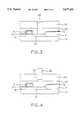
- FIG. 1is a cross section view of a semiconductor wafer illustrating the formation of an isolation layer and a nitride layer on a semiconductor substrate;
- FIG. 2is a cross section view of a semiconductor wafer illustrating the formation of a first polysilicon layer on a semiconductor substrate;
- FIG. 3is a cross section view of a semiconductor wafer illustrating the etching of the first polysilicon layer
- FIG. 4is a cross section view of a semiconductor wafer illustrating the formation of the silicon oxide plug
- FIG. 5is a cross section view of a semiconductor wafer illustrating the stripping of the nitride layer and the formation of a second polysilicon layer;
- FIG. 6is a cross section view of a semiconductor wafer illustrating the formation of the side wall spacer
- FIG. 7is a cross section view of a semiconductor wafer illustrating the formation of a dielectric layer on the first polysilicon layer.
- FIG. 8is a cross section view of a semiconductor wafer illustrating formation of a third polysilicon layer on the dielectric layer.
- DRAMDynamic Random Access Memory
- FIG. 1a silicon wafer is illustrated in cross-section.
- the silicon waferincludes a single crystal substrate 2, a field oxide 4, gate electrodes 6, contact windows 8, and impurity regions 10.
- the single crystal substrate 2is P-type with a ⁇ 100>crystallographic orientation.
- the field oxide (FOX)4is created for purposes of isolating the adjacent structures.
- FOX 4 regionis created using well known photolithography and dry etching steps. This process consists of creating a photolithographic mask containing the pattern of the component to be formed, coating the wafer with a light sensitive material called a photoresist, exposing the photoresist coated wafer to ultraviolet light through the mask to soften or harden parts of the photoresist (depending on whether positive or negative photoresist is used), removing the softened parts of the photoresist, etching to remove the materials left unprotected by the photoresist and stripping the remaining photoresist.
- This photolithographic masking and etching processis commonly referred to as "patterning and etching”.
- a silicon nitride-silicon dioxide composite layeris deposited onto the substrate 2.
- a photoresistis applied to the composite layer that delineates the FOX 4 region. After the photoresist is removed, and wet cleaned, thermal oxidation in an oxygen stem environment is used to form FOX 4.
- FOX 4has a thickness of about 4000-6000 angstroms.
- a MOS transistoris formed in the substrate 2.
- the transistorincludes a gate electrode 6 formed on substrate 2, with source and drain impurity regions 10 formed in the substrate 2 between the gate electrodes 6.
- the formation of the access transistors for DRAMsis well known in the art and are not particularly germane to the present invention. Thus, only a cursory description of forming access transistors is given here.
- An oxide layer 12is formed over the gate electrodes 6, the impurity regions 10, and the FOX 4.
- the oxide layer 12is composed of nitride or undoped oxide layer.
- the oxide layer 12is deposited using any suitable deposition process, to a thickness of about 500-2000 angstroms.
- a conventional etching stepis used to etch the oxide layer 12 to expose one of the impurity regions 10.
- an isolation layer 14is formed over the oxide layer 12 and the exposed impurity region 10 using low pressure chemical vapor deposition (LPCVD). It can be appreciated that other methods of depositing the isolation layer 14 can also be used.
- the isolation layer 14is made of borophosphosilicate glass (BPSG). The thickness of the BPSG layer 14 is between about 3000-6000 angstroms.
- a second nitride layer 16is formed on the BPSG layer 14, having a thickness about 3000-8000 angstroms.
- a contact window 8is formed to allow the source and drain of the transistor to be electrically connected to the capacitor of the present invention.
- the contact window 8is formed using any suitable pattern and etching technique.
- a first polysilicon layer 20is formed on the nitride layer 16, whereby the contact hole 18 is filled with the first polysilicon layer 20.
- the first polysilicon layer 20is formed of low pressure chemical vapor deposition of doped polysilicon or in-situ phosphorus doped polysilicon.
- an anisotropic etching processis performed to etch back the first polysilicon layer 20 until the surface of the nitride layer 16 is exposed.
- a polysilicon plug 20is generated as a node contact.
- the width of the node contactis about 0.3-0.7 micron meter.
- a thermal oxidation stepis performed to grow a silicon dioxide plug 22 from the upper portion of the polysilicon plug 20.
- the temperature of the thermal oxidationis about 750°-850° C.
- a high pressure thermal oxdationis used.
- the oxide plug 22extends out of the contact hole and above the nitride layer 16, but does not extend below the lower surface of the nitride layer 16.
- the nitride layer 16is stripped using a conventional oxygen plasma etching technique. As a result, the sidewalls of the upper portion of the remaining polysilicon plug 20 is exposed. Then a second polysilicon layer 24 is formed on the BPSG layer 14, the sidewalls of the upper portion of the polysilicon plug 20, and the silicon dioxide plug 22.
- the second polysilicon layer 24is deposited using any suitable deposition technique.
- the second polysilicon layer 24can be doped polysilicon or in-situ doped polysilicon. In this embodiment, the thickness of the second polysilicon layer 24 is about 500-2000 angstroms.
- the second polysilicon layer 24is anisotropically etched using a dry etching process until the top surface of the oxide plug 22 is exposed. As a result, a polysilicon spacer 26 is formed around the oxide plug 22 and the upper portion of the polysilicon plug 20.
- the silicon dioxide plug 22is removed by dry etching.
- this dry etch stepremoves an upper portion of the BPSG layer 14.
- the oxide layer 12can be replaced with a nitride layer.
- this dry etching stepcan be continued to totally remove the BPSG layer 14.
- the polysilicon spacer 26 and the polysilicon plug 20form a node (or bottom storage) electrode of a capacitor for a DRAM cell.
- a dielectric film 28is formed along the surface of the polysilicon spacer 26 and the first polysilicon layer 20.
- the dielectric film 28is can be formed from a double film of nitride/oxide film, a triple form of oxide/nitride/oxide, or any other high dielectric film such as tantalum oxide (Ta 2 O 5 ).
- the resultant structureis shown in FIG. 7.
- a third polysilicon layer 30is formed atop the entire structure of FIG. 7.
- the third polysilicon layeris formed of low pressure chemical vapor deposition.
- the third polysilicon layer 30is formed of doped polysilicon or in-situ doped polysilicon.
- the thickness of the thire polysiliconis about 1000-2000 angstroms.
- the third polysilicon layer 30is then patterned and etched to form the upper electrode of the DRAM cell capacitor.
- the resulting capacitoris formed from the first polysilicon layer 20, the polysilicon spacer 26, the dielectric film 28, and the third polysilicon layer 30.
- the first polysilicon layer 20 and second polysilicon layer 24are used to form bottom storage electrode while the third polysilicon layer 30 is served as top storage electrode.
Landscapes
- Engineering & Computer Science (AREA)
- Manufacturing & Machinery (AREA)
- Semiconductor Memories (AREA)
Abstract
Description
Claims (20)
Priority Applications (1)
| Application Number | Priority Date | Filing Date | Title |
|---|---|---|---|
| US08/666,801US5677221A (en) | 1996-06-19 | 1996-06-19 | Method of manufacture DRAM capacitor with reduced layout area |
Applications Claiming Priority (1)
| Application Number | Priority Date | Filing Date | Title |
|---|---|---|---|
| US08/666,801US5677221A (en) | 1996-06-19 | 1996-06-19 | Method of manufacture DRAM capacitor with reduced layout area |
Publications (1)
| Publication Number | Publication Date |
|---|---|
| US5677221Atrue US5677221A (en) | 1997-10-14 |
Family
ID=24675545
Family Applications (1)
| Application Number | Title | Priority Date | Filing Date |
|---|---|---|---|
| US08/666,801Expired - LifetimeUS5677221A (en) | 1996-06-19 | 1996-06-19 | Method of manufacture DRAM capacitor with reduced layout area |
Country Status (1)
| Country | Link |
|---|---|
| US (1) | US5677221A (en) |
Cited By (49)
| Publication number | Priority date | Publication date | Assignee | Title |
|---|---|---|---|---|
| US5824582A (en)* | 1997-06-04 | 1998-10-20 | Vanguard International Semiconductor Corporation | Stack DRAM cell manufacturing process with high capacitance capacitor |
| US5907772A (en)* | 1996-02-26 | 1999-05-25 | Nec Corporation | Method of producing cylindrical storage node of stacked capacitor in memory cell |
| US6100129A (en)* | 1998-11-09 | 2000-08-08 | Worldwide Semiconductor Manufacturing Corporation | Method for making fin-trench structured DRAM capacitor |
| US6518070B1 (en)* | 1997-12-22 | 2003-02-11 | Motorola, Inc. | Process of forming a semiconductor device and a semiconductor device |
| US6713398B2 (en)* | 1999-10-18 | 2004-03-30 | Taiwan Semiconductor Manufacturing Co., Ltd. | Method of planarizing polysillicon plug |
| US20060043617A1 (en)* | 2004-08-30 | 2006-03-02 | Abbott Todd R | DRAM layout with vertical FETs and method of formation |
| CN100463185C (en)* | 2005-08-16 | 2009-02-18 | 力晶半导体股份有限公司 | Dynamic random access memory and manufacturing method thereof |
| US20130231620A1 (en)* | 2006-02-28 | 2013-09-05 | Coloplast A/S | Leak sensor |
| US10531977B2 (en) | 2014-04-17 | 2020-01-14 | Coloplast A/S | Thermoresponsive skin barrier appliances |
| US10849781B2 (en) | 2017-12-22 | 2020-12-01 | Coloplast A/S | Base plate for an ostomy appliance |
| US11534323B2 (en) | 2017-12-22 | 2022-12-27 | Coloplast A/S | Tools and methods for placing a medical appliance on a user |
| US11540937B2 (en) | 2017-12-22 | 2023-01-03 | Coloplast A/S | Base plate and sensor assembly of a medical system having a leakage sensor |
| US11547596B2 (en) | 2017-12-22 | 2023-01-10 | Coloplast A/S | Ostomy appliance with layered base plate |
| US11589811B2 (en) | 2017-12-22 | 2023-02-28 | Coloplast A/S | Monitor device of a medical system and associated method for operating a monitor device |
| US11590015B2 (en) | 2017-12-22 | 2023-02-28 | Coloplast A/S | Sensor assembly part and a base plate for a medical appliance and a method for manufacturing a sensor assembly part and a base plate |
| US11607334B2 (en) | 2017-12-22 | 2023-03-21 | Coloplast A/S | Base plate for a medical appliance, a monitor device and a system for a medical appliance |
| US11612508B2 (en) | 2017-12-22 | 2023-03-28 | Coloplast A/S | Sensor assembly part for a medical appliance and a method for manufacturing a sensor assembly part |
| US11612512B2 (en) | 2019-01-31 | 2023-03-28 | Coloplast A/S | Moisture detecting base plate for an ostomy appliance and a system for determining moisture propagation in a base plate and/or a sensor assembly part |
| US11627891B2 (en) | 2017-12-22 | 2023-04-18 | Coloplast A/S | Calibration methods for medical appliance tools |
| US11628084B2 (en) | 2017-12-22 | 2023-04-18 | Coloplast A/S | Sensor assembly part and a base plate for a medical appliance and a device for connecting to a base plate or a sensor assembly part |
| US11654043B2 (en) | 2017-12-22 | 2023-05-23 | Coloplast A/S | Sensor assembly part and a base plate for a medical appliance and a method for manufacturing a base plate or a sensor assembly part |
| US11701248B2 (en) | 2017-12-22 | 2023-07-18 | Coloplast A/S | Accessory devices of a medical system, and related methods for communicating leakage state |
| US11707376B2 (en) | 2017-12-22 | 2023-07-25 | Coloplast A/S | Base plate for a medical appliance and a sensor assembly part for a base plate and a method for manufacturing a base plate and sensor assembly part |
| US11707377B2 (en) | 2017-12-22 | 2023-07-25 | Coloplast A/S | Coupling part with a hinge for a medical base plate and sensor assembly part |
| US11717433B2 (en) | 2017-12-22 | 2023-08-08 | Coloplast A/S | Medical appliance with angular leakage detection |
| US11786392B2 (en) | 2017-12-22 | 2023-10-17 | Coloplast A/S | Data collection schemes for an ostomy appliance and related methods |
| US11819443B2 (en) | 2017-12-22 | 2023-11-21 | Coloplast A/S | Moisture detecting base plate for a medical appliance and a system for determining moisture propagation in a base plate and/or a sensor assembly part |
| US11865029B2 (en) | 2017-12-22 | 2024-01-09 | Coloplast A/S | Monitor device of a medical system having a connector for coupling to both a base plate and an accessory device |
| US11872154B2 (en) | 2017-12-22 | 2024-01-16 | Coloplast A/S | Medical appliance system, monitor device, and method of monitoring a medical appliance |
| US11918506B2 (en) | 2017-12-22 | 2024-03-05 | Coloplast A/S | Medical appliance with selective sensor points and related methods |
| US11931285B2 (en) | 2018-02-20 | 2024-03-19 | Coloplast A/S | Sensor assembly part and a base plate for a medical appliance and a device for connecting to a base plate and/or a sensor assembly part |
| US11986418B2 (en) | 2017-12-22 | 2024-05-21 | Coloplast A/S | Medical system and monitor device with angular leakage detection |
| US11998473B2 (en) | 2017-12-22 | 2024-06-04 | Coloplast A/S | Tools and methods for cutting holes in a medical appliance |
| US11998474B2 (en) | 2018-03-15 | 2024-06-04 | Coloplast A/S | Apparatus and methods for navigating ostomy appliance user to changing room |
| US12029582B2 (en) | 2018-02-20 | 2024-07-09 | Coloplast A/S | Accessory devices of a medical system, and related methods for changing a medical appliance based on future operating state |
| US12064258B2 (en) | 2018-12-20 | 2024-08-20 | Coloplast A/S | Ostomy condition classification with image data transformation, devices and related methods |
| US12064369B2 (en) | 2017-12-22 | 2024-08-20 | Coloplast A/S | Processing schemes for an ostomy system, monitor device for an ostomy appliance and related methods |
| US12147357B2 (en) | 2020-04-14 | 2024-11-19 | Coloplast A/S | Personal care system with monitor device and related methods |
| US12165312B2 (en) | 2018-12-20 | 2024-12-10 | Coloplast A/S | Ostomy condition classification with masking, devices and related methods |
| US12171572B2 (en) | 2017-12-22 | 2024-12-24 | Coloplast A/S | Accessory devices of a medical system, and related methods for communicating operating state |
| US12178740B2 (en) | 2017-12-22 | 2024-12-31 | Coloplast A/S | Leakage detection in an ostomy device |
| US12208029B2 (en) | 2018-02-20 | 2025-01-28 | Coloplast A/S | Base plate having a mechanical and electrical connector |
| US12226229B2 (en) | 2018-03-15 | 2025-02-18 | Coloplast A/S | Methods of configuring ostomy notifications and related accessory devices |
| US12232997B2 (en) | 2018-08-15 | 2025-02-25 | Coloplast A/S | Accessory device of a medical system and related methods for issue identification |
| US12232998B2 (en) | 2019-01-31 | 2025-02-25 | Coloplast A/S | Application of a stomal sensor patch |
| US12257172B2 (en) | 2019-02-28 | 2025-03-25 | Coloplast A/S | Sensor patch for attachment to a base plate |
| US12272449B2 (en) | 2017-12-22 | 2025-04-08 | Coloplast A/S | Data transmission schemes for a medical system, monitor device for a medical appliance and related methods |
| US12310877B2 (en) | 2019-01-31 | 2025-05-27 | Coloplast A/S | Sensor patch for an ostomy appliance |
| US12376984B2 (en) | 2019-01-31 | 2025-08-05 | Coloplast A/S | Stomal sensor patch |
Citations (4)
| Publication number | Priority date | Publication date | Assignee | Title |
|---|---|---|---|---|
| US5137842A (en)* | 1991-05-10 | 1992-08-11 | Micron Technology, Inc. | Stacked H-cell capacitor and process to fabricate same |
| US5399518A (en)* | 1992-07-15 | 1995-03-21 | Samsung Electronics Co., Ltd. | Method for manufacturing a multiple walled capacitor of a semiconductor device |
| US5478769A (en)* | 1993-12-28 | 1995-12-26 | Hyundai Electronics Industries Co., Ltd. | Process for fabricating a stashed capacitor in a semiconductor device |
| US5510289A (en)* | 1994-06-22 | 1996-04-23 | Hyundai Electronics Industries Co. Ltd. | Method for fabricating stack capacitor of semiconductor device |
- 1996
- 1996-06-19USUS08/666,801patent/US5677221A/ennot_activeExpired - Lifetime
Patent Citations (4)
| Publication number | Priority date | Publication date | Assignee | Title |
|---|---|---|---|---|
| US5137842A (en)* | 1991-05-10 | 1992-08-11 | Micron Technology, Inc. | Stacked H-cell capacitor and process to fabricate same |
| US5399518A (en)* | 1992-07-15 | 1995-03-21 | Samsung Electronics Co., Ltd. | Method for manufacturing a multiple walled capacitor of a semiconductor device |
| US5478769A (en)* | 1993-12-28 | 1995-12-26 | Hyundai Electronics Industries Co., Ltd. | Process for fabricating a stashed capacitor in a semiconductor device |
| US5510289A (en)* | 1994-06-22 | 1996-04-23 | Hyundai Electronics Industries Co. Ltd. | Method for fabricating stack capacitor of semiconductor device |
Cited By (80)
| Publication number | Priority date | Publication date | Assignee | Title |
|---|---|---|---|---|
| US5907772A (en)* | 1996-02-26 | 1999-05-25 | Nec Corporation | Method of producing cylindrical storage node of stacked capacitor in memory cell |
| US5824582A (en)* | 1997-06-04 | 1998-10-20 | Vanguard International Semiconductor Corporation | Stack DRAM cell manufacturing process with high capacitance capacitor |
| US6518070B1 (en)* | 1997-12-22 | 2003-02-11 | Motorola, Inc. | Process of forming a semiconductor device and a semiconductor device |
| US6100129A (en)* | 1998-11-09 | 2000-08-08 | Worldwide Semiconductor Manufacturing Corporation | Method for making fin-trench structured DRAM capacitor |
| US6713398B2 (en)* | 1999-10-18 | 2004-03-30 | Taiwan Semiconductor Manufacturing Co., Ltd. | Method of planarizing polysillicon plug |
| US20080237776A1 (en)* | 2004-08-30 | 2008-10-02 | Abbott Todd R | DRAM layout with vertical FETs and method of formation |
| US8389360B2 (en) | 2004-08-30 | 2013-03-05 | Micron Technology, Inc. | DRAM layout with vertical FETs and method of formation |
| US7365385B2 (en) | 2004-08-30 | 2008-04-29 | Micron Technology, Inc. | DRAM layout with vertical FETs and method of formation |
| US20060043617A1 (en)* | 2004-08-30 | 2006-03-02 | Abbott Todd R | DRAM layout with vertical FETs and method of formation |
| US20060125123A1 (en)* | 2004-08-30 | 2006-06-15 | Abbott Todd R | DRAM layout with vertical FETs and method of formation |
| US7560336B2 (en) | 2004-08-30 | 2009-07-14 | Micron Technology, Inc. | DRAM layout with vertical FETs and method of formation |
| US7968928B2 (en) | 2004-08-30 | 2011-06-28 | Micron Technology, Inc. | DRAM layout with vertical FETs and method of formation |
| US20110217819A1 (en)* | 2004-08-30 | 2011-09-08 | Abbott Todd R | Dram layout with vertical fets and method of formation |
| CN100463185C (en)* | 2005-08-16 | 2009-02-18 | 力晶半导体股份有限公司 | Dynamic random access memory and manufacturing method thereof |
| US20130231620A1 (en)* | 2006-02-28 | 2013-09-05 | Coloplast A/S | Leak sensor |
| US9216104B2 (en)* | 2006-02-28 | 2015-12-22 | Coloplast A/S | Leak sensor |
| US10016298B2 (en) | 2006-02-28 | 2018-07-10 | Coloplast A/G | Method of detecting detachment of an ostomy device from a patient |
| US11096818B2 (en) | 2006-02-28 | 2021-08-24 | Coloplast A/S | Ostomy appliance having an electrode |
| US10531977B2 (en) | 2014-04-17 | 2020-01-14 | Coloplast A/S | Thermoresponsive skin barrier appliances |
| US11819443B2 (en) | 2017-12-22 | 2023-11-21 | Coloplast A/S | Moisture detecting base plate for a medical appliance and a system for determining moisture propagation in a base plate and/or a sensor assembly part |
| US12004990B2 (en) | 2017-12-22 | 2024-06-11 | Coloplast A/S | Ostomy base plate having a monitor interface provided with a lock to hold a data monitor in mechanical and electrical connection with electrodes of the base plate |
| US11540937B2 (en) | 2017-12-22 | 2023-01-03 | Coloplast A/S | Base plate and sensor assembly of a medical system having a leakage sensor |
| US11547595B2 (en) | 2017-12-22 | 2023-01-10 | Coloplast A/S | Base plate and a sensor assembly part for a medical appliance |
| US11547596B2 (en) | 2017-12-22 | 2023-01-10 | Coloplast A/S | Ostomy appliance with layered base plate |
| US11589811B2 (en) | 2017-12-22 | 2023-02-28 | Coloplast A/S | Monitor device of a medical system and associated method for operating a monitor device |
| US11590015B2 (en) | 2017-12-22 | 2023-02-28 | Coloplast A/S | Sensor assembly part and a base plate for a medical appliance and a method for manufacturing a sensor assembly part and a base plate |
| US11607334B2 (en) | 2017-12-22 | 2023-03-21 | Coloplast A/S | Base plate for a medical appliance, a monitor device and a system for a medical appliance |
| US11612508B2 (en) | 2017-12-22 | 2023-03-28 | Coloplast A/S | Sensor assembly part for a medical appliance and a method for manufacturing a sensor assembly part |
| US12433782B2 (en) | 2017-12-22 | 2025-10-07 | Coloplast A/S | Ostomy appliance with selective sensor points and related methods |
| US11612509B2 (en) | 2017-12-22 | 2023-03-28 | Coloplast A/S | Base plate and a sensor assembly part for an ostomy appliance |
| US11622719B2 (en) | 2017-12-22 | 2023-04-11 | Coloplast A/S | Sensor assembly part, base plate and monitor device of a medical system and associated method |
| US11627891B2 (en) | 2017-12-22 | 2023-04-18 | Coloplast A/S | Calibration methods for medical appliance tools |
| US11628084B2 (en) | 2017-12-22 | 2023-04-18 | Coloplast A/S | Sensor assembly part and a base plate for a medical appliance and a device for connecting to a base plate or a sensor assembly part |
| US11654043B2 (en) | 2017-12-22 | 2023-05-23 | Coloplast A/S | Sensor assembly part and a base plate for a medical appliance and a method for manufacturing a base plate or a sensor assembly part |
| US11701248B2 (en) | 2017-12-22 | 2023-07-18 | Coloplast A/S | Accessory devices of a medical system, and related methods for communicating leakage state |
| US11707376B2 (en) | 2017-12-22 | 2023-07-25 | Coloplast A/S | Base plate for a medical appliance and a sensor assembly part for a base plate and a method for manufacturing a base plate and sensor assembly part |
| US11707377B2 (en) | 2017-12-22 | 2023-07-25 | Coloplast A/S | Coupling part with a hinge for a medical base plate and sensor assembly part |
| US11717433B2 (en) | 2017-12-22 | 2023-08-08 | Coloplast A/S | Medical appliance with angular leakage detection |
| US11730622B2 (en) | 2017-12-22 | 2023-08-22 | Coloplast A/S | Medical appliance with layered base plate and/or sensor assembly part and related methods |
| US12433781B2 (en) | 2017-12-22 | 2025-10-07 | Coloplast A/S | Tools and methods for placing an ostomy appliance on a user |
| US11786392B2 (en) | 2017-12-22 | 2023-10-17 | Coloplast A/S | Data collection schemes for an ostomy appliance and related methods |
| US10849781B2 (en) | 2017-12-22 | 2020-12-01 | Coloplast A/S | Base plate for an ostomy appliance |
| US11844718B2 (en) | 2017-12-22 | 2023-12-19 | Coloplast A/S | Medical device having a monitor mechanically and electrically attachable to a medical appliance |
| US11865029B2 (en) | 2017-12-22 | 2024-01-09 | Coloplast A/S | Monitor device of a medical system having a connector for coupling to both a base plate and an accessory device |
| US11872154B2 (en) | 2017-12-22 | 2024-01-16 | Coloplast A/S | Medical appliance system, monitor device, and method of monitoring a medical appliance |
| US11918506B2 (en) | 2017-12-22 | 2024-03-05 | Coloplast A/S | Medical appliance with selective sensor points and related methods |
| US12364621B2 (en) | 2017-12-22 | 2025-07-22 | Coloplast A/S | Ostomy system operable to inform an ostomate of an ostomy device condition useful in preventing leakage relative to the ostomy device |
| US11974938B2 (en) | 2017-12-22 | 2024-05-07 | Coloplast A/S | Ostomy system having an ostomy appliance, a monitor device, and a docking station for the monitor device |
| US11986418B2 (en) | 2017-12-22 | 2024-05-21 | Coloplast A/S | Medical system and monitor device with angular leakage detection |
| US11998473B2 (en) | 2017-12-22 | 2024-06-04 | Coloplast A/S | Tools and methods for cutting holes in a medical appliance |
| US12290466B2 (en) | 2017-12-22 | 2025-05-06 | Coloplast A/S | Accessory devices of an ostomy system, and related methods for communicating leakage state |
| US11534323B2 (en) | 2017-12-22 | 2022-12-27 | Coloplast A/S | Tools and methods for placing a medical appliance on a user |
| US12272449B2 (en) | 2017-12-22 | 2025-04-08 | Coloplast A/S | Data transmission schemes for a medical system, monitor device for a medical appliance and related methods |
| US12232999B2 (en) | 2017-12-22 | 2025-02-25 | Coloplast A/S | Base plate and a sensor assembly part for an ostomy appliance |
| US12064369B2 (en) | 2017-12-22 | 2024-08-20 | Coloplast A/S | Processing schemes for an ostomy system, monitor device for an ostomy appliance and related methods |
| US12097141B2 (en) | 2017-12-22 | 2024-09-24 | Coloplast A/S | Medical system having a monitor attachable to an ostomy appliance and to a docking station |
| US12127966B2 (en) | 2017-12-22 | 2024-10-29 | Coloplast A/S | Base plate and sensor assembly of an ostomy system having a leakage sensor |
| US12138074B2 (en) | 2017-12-22 | 2024-11-12 | Coloplast A/S | Monitor device of an ostomy system and associated method for operating a monitor device |
| US12208030B2 (en) | 2017-12-22 | 2025-01-28 | Coloplast A/S | Ostomy appliance system, monitor device, and method of monitoring an ostomy appliance |
| US12161581B2 (en) | 2017-12-22 | 2024-12-10 | Coloplast A/S | Method of monitoring performance of an ostomy device with a monitor device attachable to both an ostomy appliance and an accessory device |
| US12178737B2 (en) | 2017-12-22 | 2024-12-31 | Coloplast A/S | Adhesive ostomy base plate having a sensor assembly adapted to monitor a condition of the adhesive |
| US12171572B2 (en) | 2017-12-22 | 2024-12-24 | Coloplast A/S | Accessory devices of a medical system, and related methods for communicating operating state |
| US12178736B2 (en) | 2017-12-22 | 2024-12-31 | Coloplast A/S | Ostomy system base plate including electrical terminals and a coupling part attachable to a monitor device |
| US12178740B2 (en) | 2017-12-22 | 2024-12-31 | Coloplast A/S | Leakage detection in an ostomy device |
| US12178739B2 (en) | 2017-12-22 | 2024-12-31 | Coloplast A/S | Ostomy appliance having an electrical connector |
| US12029582B2 (en) | 2018-02-20 | 2024-07-09 | Coloplast A/S | Accessory devices of a medical system, and related methods for changing a medical appliance based on future operating state |
| US12208029B2 (en) | 2018-02-20 | 2025-01-28 | Coloplast A/S | Base plate having a mechanical and electrical connector |
| US11931285B2 (en) | 2018-02-20 | 2024-03-19 | Coloplast A/S | Sensor assembly part and a base plate for a medical appliance and a device for connecting to a base plate and/or a sensor assembly part |
| US11998474B2 (en) | 2018-03-15 | 2024-06-04 | Coloplast A/S | Apparatus and methods for navigating ostomy appliance user to changing room |
| US12226229B2 (en) | 2018-03-15 | 2025-02-18 | Coloplast A/S | Methods of configuring ostomy notifications and related accessory devices |
| US12232997B2 (en) | 2018-08-15 | 2025-02-25 | Coloplast A/S | Accessory device of a medical system and related methods for issue identification |
| US12064258B2 (en) | 2018-12-20 | 2024-08-20 | Coloplast A/S | Ostomy condition classification with image data transformation, devices and related methods |
| US12165312B2 (en) | 2018-12-20 | 2024-12-10 | Coloplast A/S | Ostomy condition classification with masking, devices and related methods |
| US12232998B2 (en) | 2019-01-31 | 2025-02-25 | Coloplast A/S | Application of a stomal sensor patch |
| US12310877B2 (en) | 2019-01-31 | 2025-05-27 | Coloplast A/S | Sensor patch for an ostomy appliance |
| US12376984B2 (en) | 2019-01-31 | 2025-08-05 | Coloplast A/S | Stomal sensor patch |
| US11737907B2 (en) | 2019-01-31 | 2023-08-29 | Coloplast A/S | Moisture detecting base plate for an ostomy appliance and a system for determining moisture propagation in a base plate and/or a sensor assembly part |
| US11612512B2 (en) | 2019-01-31 | 2023-03-28 | Coloplast A/S | Moisture detecting base plate for an ostomy appliance and a system for determining moisture propagation in a base plate and/or a sensor assembly part |
| US12257172B2 (en) | 2019-02-28 | 2025-03-25 | Coloplast A/S | Sensor patch for attachment to a base plate |
| US12147357B2 (en) | 2020-04-14 | 2024-11-19 | Coloplast A/S | Personal care system with monitor device and related methods |
Similar Documents
| Publication | Publication Date | Title |
|---|---|---|
| US5677221A (en) | Method of manufacture DRAM capacitor with reduced layout area | |
| US5656536A (en) | Method of manufacturing a crown shaped capacitor with horizontal fins for high density DRAMs | |
| US5284787A (en) | Method of making a semiconductor memory device having improved electrical characteristics | |
| US5821139A (en) | Method for manufacturing a DRAM with increased electrode surface area | |
| US5837576A (en) | Method for forming a capacitor using a silicon oxynitride etching stop layer | |
| US5913118A (en) | Method of manufacturing trench DRAM cells with self-aligned field plate | |
| US5966612A (en) | Method of making a multiple mushroom shape capacitor for high density DRAMs | |
| US6403431B1 (en) | Method of forming in an insulating layer a trench that exceeds the photolithographic resolution limits | |
| US6150213A (en) | Method of forming a cob dram by using self-aligned node and bit line contact plug | |
| US5770510A (en) | Method for manufacturing a capacitor using non-conformal dielectric | |
| US5933742A (en) | Multi-crown capacitor for high density DRAMS | |
| US5913129A (en) | Method of fabricating a capacitor structure for a dynamic random access memory | |
| US5691223A (en) | Method of fabricating a capacitor over a bit line DRAM process | |
| US5763304A (en) | Method for manufacturing a capacitor with chemical mechanical polishing | |
| US5952039A (en) | Method for manufacturing DRAM capacitor | |
| US5677223A (en) | Method for manufacturing a DRAM with reduced cell area | |
| US5814549A (en) | Method of making porous-si capacitor dram cell | |
| US6057205A (en) | Method to form a ragged poly-Si structure for high density DRAM cells | |
| US6146937A (en) | Method of forming a DRAM device utilizing a sacrificial doped oxide layer | |
| US5484744A (en) | Method for fabricating a stacked capacitor for dynamic random access memory cell | |
| US5976981A (en) | Method for manufacturing a reverse crown capacitor for DRAM memory cell | |
| US5830792A (en) | Method of making a stack capacitor in a DRAM cell | |
| US5932115A (en) | Method of manufacturing a crown shape capacitor | |
| KR100408423B1 (en) | Semiconductor memory device for reducing parasitic capacitance and fabrication method thereof | |
| US5804489A (en) | Method of manufacturing a crown shape capacitor in semiconductor memory using a single step etching |
Legal Events
| Date | Code | Title | Description |
|---|---|---|---|
| AS | Assignment | Owner name:VANGUARD INTERNATIONAL SEMICONDUCTOR CORPORATION, Free format text:ASSIGNMENT OF ASSIGNORS INTEREST;ASSIGNOR:TSENG, HORNG-HUEI;REEL/FRAME:008056/0382 Effective date:19960607 | |
| STCF | Information on status: patent grant | Free format text:PATENTED CASE | |
| FPAY | Fee payment | Year of fee payment:4 | |
| FEPP | Fee payment procedure | Free format text:PAYOR NUMBER ASSIGNED (ORIGINAL EVENT CODE: ASPN); ENTITY STATUS OF PATENT OWNER: LARGE ENTITY | |
| FPAY | Fee payment | Year of fee payment:8 | |
| FPAY | Fee payment | Year of fee payment:12 | |
| FEPP | Fee payment procedure | Free format text:PAYER NUMBER DE-ASSIGNED (ORIGINAL EVENT CODE: RMPN); ENTITY STATUS OF PATENT OWNER: LARGE ENTITY Free format text:PAYOR NUMBER ASSIGNED (ORIGINAL EVENT CODE: ASPN); ENTITY STATUS OF PATENT OWNER: LARGE ENTITY | |
| AS | Assignment | Owner name:TAIWAN SEMICONDUCTOR MANUFACTURING CO., LTD., TAIW Free format text:ASSIGNMENT OF ASSIGNORS INTEREST;ASSIGNOR:VANGUARD INTERNATIONAL SEMICONDUCTOR CORPORATION;REEL/FRAME:025645/0397 Effective date:20101026 |