US5673423A - Method and apparatus for aligning the operation of a plurality of processors - Google Patents
Method and apparatus for aligning the operation of a plurality of processorsDownload PDFInfo
- Publication number
- US5673423A US5673423AUS08/344,260US34426094AUS5673423AUS 5673423 AUS5673423 AUS 5673423AUS 34426094 AUS34426094 AUS 34426094AUS 5673423 AUS5673423 AUS 5673423A
- Authority
- US
- United States
- Prior art keywords
- alignment
- instruction
- processors
- processor
- request
- Prior art date
- Legal status (The legal status is an assumption and is not a legal conclusion. Google has not performed a legal analysis and makes no representation as to the accuracy of the status listed.)
- Expired - Fee Related
Links
Images

Classifications
- G—PHYSICS
- G06—COMPUTING OR CALCULATING; COUNTING
- G06F—ELECTRIC DIGITAL DATA PROCESSING
- G06F9/00—Arrangements for program control, e.g. control units
- G06F9/06—Arrangements for program control, e.g. control units using stored programs, i.e. using an internal store of processing equipment to receive or retain programs
- G06F9/46—Multiprogramming arrangements
- G06F9/52—Program synchronisation; Mutual exclusion, e.g. by means of semaphores
Definitions
- Thisrelates to multi-processors and in particular to a system for aligning the operation of a plurality of processors in a multi-processor.
- the Connection Machine Computercomprises a central computer, a microcontroller, and an array of as many as 65,536 parallel processors in presently available embodiments.
- the central computermay be a suitably programmed commercially available computer such as a Symbolics 3600-series LISP Machine.
- the microcontrolleris an instruction sequencer of conventional design for generating a sequence of instructions that are applied to the array of parallel processors by means of a thirty-two bit parallel bus.
- the microcontrollerreceives from the parallel processing array a signal which is a general purpose or GLOBAL signal that can be used for data output and status information.
- Synchronizationmay be effected by having each processor set a bit in a register when the processor reaches a point in its program where it is to be aligned with other processors. Upon reaching this synchronization point, each processor tests the register to determine if all bits have been properly set and no processor goes forward in its program until all such bits have been set. As a result of this technique, processors may be brought into strict time synchronization such that at each synchronization point each processor performs a predetermined operation at the same time.
- alignmentIn many operations, it is not necessary to achieve strict time synchronization in the operations of a plurality of processors. Rather it is sufficient to ensure simply that each processor has performed a specified task before any processor can initiate another specified task. This less strict form of synchronization is referred to herein as alignment.
- the apparatuspreferably comprises an alignment unit associated with each processor and a logic network for combining the output of the alignment units and for broadcasting information to these units. Alignment is achieved by inserting in the instruction stream from each processor that is to be aligned a request for alignment and by causing all such processors to wait until they have all made the request for alignment and completed any necessary operations.
- the alignment unit associated with each processormonitors the instruction stream to detect a request for alignment.
- the logic networkillustratively is an array of AND gates that tests each alignment unit to determine if it has detected a request for alignment and tests the processors and/or their interconnection network to determine if all necessary operations have been completed. When all the units have made such a request and all necessary operations have been completed, the logic network informs the alignment units; and the alignment units inform the processors.
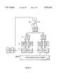
- FIG. 1is a block diagram illustrating an illustrative embodiment of a multi-processor which incorporates the invention
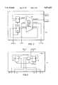
- FIG. 2is a block diagram illustrating an illustrative embodiment of the alignment unit of the present invention
- FIG. 3is an illustrative embodiment of a unit of combinatorial logic of the present invention.
- FIG. 4is a state diagram illustrating the operation of the alignment unit of FIG. 2.
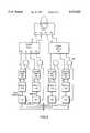
- FIG. 5is a block diagram of a second illustrative embodiment of the invention.
- illustrative apparatus of the present inventioncomprises an array of processors 10, an array of alignment units 20, an array of combinatorial logic cells 30, an interconnection network 40 and a control unit 50.
- each processorincludes an arithmetic/logic unit, a read/write memory, and input and output means. Numerous such processors are well known in the art.
- each processoris an 80386-type microprocessor such as that made by Intel Corporation.
- Interconnection network 40provides for communication between the processors. In particular, it permits the exchange of data and control information between one processor and another.
- Numerous interconnection networksare known in the art. See for example Wu, C. and Feng, T, tutorial; Interconnection Network for Parallel and Distributed Processing (IEEE, 1984).
- Illustrative communication networksare arrangements which connect each processor to its nearest neighbor in an orthogonal array of two or more dimensions. Two such networks are described in the above referenced '400 patent and numerous others are known in the art.
- the processors and interconnection networkare typically operated under the control of some type of control unit 50.
- control unit 50In the case of the processors and interconnection network of the Connection Machine Computer, an illustrative control unit is a Symbolics 3600 Series LISP machine and a microcontroller. Numerous other control units are used with other multi-processors.
- processors of a multi-processorit may be necessary to assure that one processor has reached a certain step in its operation before another processor can perform a specified operation. For example, if data is to be fetched from a first processor to a second, it is necessary to ensure that the data be in the first processor before the fetch occurs. To ensure that the data is there when needed, it is necessary to align the individual processors. This can be achieved by operating all the processors strictly in parallel in a SIMD environment. However, in many cases it may be advantageous to operate the processors in a MIMD environment and align only where needed.
- alignmentis achieved among a group of processors by inserting in the instruction stream of each of there processors two additional instructions: a request for alignment and a test if alignment has been achieved.
- the request for alignment instructionis issued at or after the time the instruction stream issues an instruction (such as a communication instruction) which will require the processors to be in alignment at some later time; and the test instruction is issued immediately before the point in the instruction stream where alignment must have been achieved.
- such alignmentis accomplished by inserting request and test instructions in the instruction stream so that for the above example the instruction stream is as follows:
- the request and test instructionsare inserted in the instruction stream from each processor to be aligned and all the processors wait at the test instruction until all the processors have asserted the request instruction.
- Preferred apparatus for processing such request and test instructionscomprises alignment units 20 and combinatorial logic cells 30 of the apparatus of FIG. 1.
- each processor 10is connected to an alignment unit so as to provide signals to such unit and to receive signals from it.
- each alignment unit 20comprises four D-type flip flops 21, 22, 23, 24 and combinatorial logic 26 which implements the input/output table set forth in Table I.
- each logic cell 30comprises an AND gate 33 and optionally two D-type flip flops 35, 36.
- the logic cellsare connected in the form of a binary tree with each logic cell in the lowest level of the tree being connected to a pair of alignment units 20.
- AND gate 33 of logic cell 30receives ASSERT signals on input lines 31, 32 and produces an output ASSERT signal on output line 34 (optionally, via flip-flop 36).
- a logic high signalis not asserted on an output line 34 until logic high signals are asserted on both input signal lines 31, 32 to AND gate 33.
- the output ASSERT signals from two cellsare applied as the two inputs to a logic cell 30 in the next higher level of the binary tree.
- the uppermost cell in the AND treehas an output line 34 which is input to an AND gate 60 along with a signal from interconnection network 10 which indicates that the interconnection network is empty.
- the networkis empty whenever there are no messages being routed through the network.
- a test for this conditionis conventional in some interconnection networks and the provision of a signal indicating that the network is empty is within the ordinary skill of the art. In the preferred embodiment shown in FIG. 1, a test for an empty network is made to ensure that message traffic on the interconnection network is completed.
- a ready signalis applied by AND gate 60 to an input ready line 37 to the uppermost cell of the binary tree. This signal is provided to two output ready lines 38, 39 (optionally, via flip-flop 35) which are connected respectively to the input ready lines of two cells in the next lower level of the binary tree.
- the READY signalis provided by each cell to two alignment units 20 so that the READY signal is broadcast to the entire array of alignment units 20.
- alignment units 20 and logic cells 30are such that a logic high signal is output on the ASSERT line from an alignment unit when that unit detects a REQUEST for alignment signal in the instruction stream received at the alignment unit. If and only if each alignment unit detects a REQUEST for alignment signal, output line 34 from the uppermost logic cell 30 in the binary tree will be logic high. If message traffic on processor interconnection network 10 is completed at some point after all the processors issue a REQUEST for alignment, then the empty signal will become logic high as well and the output of AND gate 60 will become logic high. As a result, a logic high READY signal will be broadcast down through logic cells 30 to all the alignment units where the logic high READY signal is recognized as a GRANT signal.
- the GRANT signalis processed by each alignment unit so as to output to the processor a single logic high ALIGN instruction for each TEST instruction in the instruction stream from the processor. If the GRANT signal is received before the TEST signal in the instruction stream, each alignment unit simply stores the GRANT signal and waits. If the TEST signal is received first, the alignment unit likewise just waits. Upon receipt of both TEST and GRANT signals, the alignment unit issues a logic high ALIGN signal to the processor, and the processor is then enabled to perform the operation for which alignment was required.
- the alignment unitcan be in any one of six states: IDLE, PENDING, BLOCKING, QUEUE, GOT and SAVE.
- the state of the alignment unitis stored in binary encoded form in flip-flops 22, 23, 24 and is provided as an input to combinatorial logic 26 along with the instruction stream INST from the processor and the GRANT signal from flip-flop 21.
- the instruction streamis the sequence of instructions that is provided to the processor and, in accordance with the invention includes three types of instructions: REQUEST for alignment, TEST, and all OTHER instructions which are represented in FIG. 4 by the symbols R, T and 0 respectively.
- the logic high GRANT signalis represented in FIG. 4 by G and the logic low GRANT signal by G.
- the different combinations of inputs to combinatorial logic 26are set forth in the three left-hand columns of Table I.
- the outputs produced by combinatorial logic 26 in response to these inputsare set forth in the three right-hand columns of Table I.
- one outputspecifies the next state of the alignment unit and the other two specify the logic level of the ALIGN and ASSERT lines. In cases where some combination of inputs is not possible, the next state has been indicated to be an ERROR and the ALIGN and ASSERT levels have been left undefined.
- each alignment unitis in the IDLE state and remains so upon receipt of any instruction in the instruction stream from the processor except for a REQUEST instruction. This is indicated by the loop labelled O G. While in the IDLE state both the ALIGN and ASSERT outputs are logic low.
- the alignment unitchanges to the PENDING state upon receipt of a REQUEST signal as detailed below; and in the PENDING state causes the ASSERT output to be logic high. If and when the ASSERT outputs of all the alignment units become logic high and the interconnection network is empty, the GRANT signal will become logic high and causing the GRANT signal to be logic high each alignment unit will producing output signals as specified in Table I. The alignment unit will ultimately return to the IDLE state if a TEST instruction and a logic low GRANT signal are received.
- the alignment unitchanges from the IDLE state to the PENDING state as indicated by the line R G in FIG. 4 and the third line of Table I. Once in the PENDING state, the alignment unit will stay there unless a logic high. GRANT signal is received. While in the PENDING state, combinatorial logic 26 will issue a logic high ASSERT signal for any of the possible combination of input signals.
- the ASSERT signalsare applied to the inputs to logic cells 30; and if all the ASSERT signals are logic high and if the connection network is empty a logic high READY will be broadcast to all the alignment units indicating that all the processors have completed the instruction (such as a communication instruction) they were required to complete and accordingly are aligned.
- This logic high READY signalis the logic high GRANT signal of Table I. If a logic high GRANT signal is received along with an OTHER instruction, the unit changes to the GOT state as indicated by the line OG in FIG. 4 and the twelfth line of Table I and issues a logic high ALIGN signal while continuing to issue a logic high ASSERT signal.
- the combinatorial logicremains in the GOT state, but drops the ASSERT signal to logic low which causes the GRANT signal to become logic low. If the GRANT signal is logic low while an OTHER instruction is received, the alignment unit switches to the SAVE state where it remains until a TEST instruction is received and then returns to the IDLE state.
- the unitchanges to the BLOCKING state if the GRANT signal is logic high or to the IDLE state if the GRANT signal is logic low and causes the ASSERT signal to become logic low.
- the BLOCKING stateprevents other alignment operations from being performed.
- the unitUpon receipt of any OTHER instruction at the alignment unit while it is in the BLOCKING state and the GRANT signal is low, the unit returns to the IDLE state as indicated by the line O G between the BLOCKING and IDLE states. If, however, another REQUEST instruction is received, the alignment unit returns to the PENDING state if the GRANT signal is logic low or to the QUEUE state if the GRANT signal is logic high. The unit will remain in QUEUE as long as the GRANT signal is high and will return to PENDING when the GRANT signal goes low.
- the alignment unitWhile in the PENDING state, if the alignment unit receives the TEST instruction while the GRANT signal is logic high, it will change to the BLOCKING state. Further operations in the BLOCKING state will be the same as described above.
- the apparatuscomprises an array of processors 110, an array of alignment units 130, an array of combinatorial logic cells 130 and an interconnection network 140.
- the processors 110, alignment units 120 and combinatorial logic cells 130may be the same as processors 10, alignment units 20 and logic cells 30 of FIG. 1 and processors 110 may be controlled by a control unit that is not shown.
- Interconnection network 140is different from that of network 40 in that it is implemented in the form of separate routers 142 and connection paths 144 between each pair of processors.
- the router for each processorproduces an output signal which is a logic high when there is no message traffic on the connection paths to or from the processor with which it is associated.
- This signalis applied as one input to an AND gate 146 which has as a second input the output of the alignment unit 130 associated with that processor.
- a high logic signalis provided by AND gate 146 to an input to logic cell 130 when there is no message traffic from the portion of the interconnection network associated with that processor and a logic high ASSERT signal has been generated by the alignment unit.
- the inventionmay be practiced in numerous environments.
- the processorsare Intel 80386 microprocessors
- the inventionmay be practiced using the IN and OUT instructions of the 80386 instruction set to provide instructions to an alignment unit and receive an ALIGN signal from such unit.
- the request for alignmentis made by each processor wherever it is necessary for inter-processor communications to have been completed before the processor can continue with its program.
- the request for alignmentis made at line 6.
- the requests for alignmentare processed by the alignment units 20 associated with each processor and are forwarded to logic cells 30 as logic high ASSERT signals. These requests are ANDed together by logic cells 30 and when all processors have made such a request a logic high signal is applied to AND gate 60. If the interconnection network is empty, a logic high READY signal is broadcast by AND gate 60 to all the alignment units 20 via logic cells 30.
- the logic level of the READY or GRANT signalis monitored by the instructions at lines 20, 21, and 22, which respectively read this signal level, test if it is a 1-bit or logic high, and recycle if the 1-bit has not been received.
- These instructionsprovide the function of the TEST instruction and the ALIGN signal of Table I.
- the processorsare all aligned at the time the READY signal goes logic high which occurs at some point between the request for alignment at line 6 and the time each processor initiates a successful test for a 1-bit in the AL register as at lines 20-23. It is not necessary, however, that each processor make such a test at the same time; and it is not necessary that the first such test be made after the READY signal goes logic high. If the logic high READY signal is received before the program reaches lines 20-21, the alignment unit will save that information until those lines are reached; and if the READY signal is still logic low when the program reaches line 20, the program will simply loop through the instructions at lines 20-22 until the READY signal goes logic high.
Landscapes
- Engineering & Computer Science (AREA)
- Software Systems (AREA)
- Theoretical Computer Science (AREA)
- Physics & Mathematics (AREA)
- General Engineering & Computer Science (AREA)
- General Physics & Mathematics (AREA)
- Multi Processors (AREA)
Abstract
Description
TABLE I ______________________________________ INPUTS OUTPUTS State INST GRANT State+1 ALIGN ASSERT ______________________________________ IDLE TEST LOW ERROR X X IDLE TEST HIGH ERROR X X IDLE REQ LOW PEND LOW LOW IDLE REQ HIGH ERROR X X IDLE OTHER LOW IDLE LOW LOW IDLE OTHER HIGH ERROR X X PEND TEST LOW PEND LOW HIGH PEND TEST HIGH BLOCK HIGH HIGH PEND REQ LOW ERROR X X PEND REQ HIGH ERROR X X PEND OTHER LOW PEND LOW HIGH PEND OTHER HIGH GOT HIGH HIGH GOT TEST LOW IDLE HIGH LOW GOT TEST HIGH BLOCK HIGH LOW GOT REQ LOW ERROR X X GOT REQ HIGH ERROR X X GOT OTHER LOW SAVE HIGH LOW GOT OTHER HIGH GOT HIGH LOW SAVE TEST LOW IDLE HIGH LOW SAVE TEST HIGH ERROR X X SAVE REQ LOW ERROR X X SAVE REQ HIGH ERROR X X SAVE OTHER LOW SAVE HIGH LOW SAVE OTHER HIGH ERROR X X BLOCK TEST LOW ERROR X X BLOCK TEST HIGH ERROR X X BLOCK REQ LOW PEND LOW LOW BLOCK REQ HIGH QUEUE LOW LOW BLOCK OTHER LOW IDLE LOW LOW BLOCK OTHER HIGH BLOCK LOW LOW QUEUE TEST LOW PEND LOW LOW QUEUE TEST HIGH QUEUE LOW LOW QUEUE REQ LOW ERROR X X QUEUE REQ HIGH ERROR X X QUEUE OTHER LOW PEND LOW LOW QUEUE OTHER HIGH QUEUE LOW LOW ______________________________________
______________________________________ 1. MOV AL, 5 load an address, 5, of the processor to which data is to be sent 2. OUT sending device, AL sand data via sending device 3. ADD AL, CL compute data of message 4. OUT sending device, AL send data via sending device 5. MOV AL, 1 load into AL a 1-bit representing a request for alignment 6. OUT align unit, AL mend the 1-bit in register AL to thealignment unit 20 . . 20. IN AL, align unit load the ALIGN signal from the alignment unit intoregister AL 21. TEST AL, 1 test if the signal in register AL is a 1-bit 22.INE 20 if not, return to instruction atline 20 23. IN AL, receiving device if it is a 1-bit, proceed with program illustratively by loading signals from receiving device into register AL ______________________________________
Claims (1)
Priority Applications (1)
| Application Number | Priority Date | Filing Date | Title |
|---|---|---|---|
| US08/344,260US5673423A (en) | 1988-02-02 | 1994-11-23 | Method and apparatus for aligning the operation of a plurality of processors |
Applications Claiming Priority (4)
| Application Number | Priority Date | Filing Date | Title |
|---|---|---|---|
| US15138688A | 1988-02-02 | 1988-02-02 | |
| US07/530,484US5222237A (en) | 1988-02-02 | 1990-05-29 | Apparatus for aligning the operation of a plurality of processors |
| US08/053,979US5388262A (en) | 1988-02-02 | 1993-04-26 | Method and apparatus for aligning the operation of a plurality of processors |
| US08/344,260US5673423A (en) | 1988-02-02 | 1994-11-23 | Method and apparatus for aligning the operation of a plurality of processors |
Related Parent Applications (1)
| Application Number | Title | Priority Date | Filing Date |
|---|---|---|---|
| US08/053,979DivisionUS5388262A (en) | 1988-02-02 | 1993-04-26 | Method and apparatus for aligning the operation of a plurality of processors |
Publications (1)
| Publication Number | Publication Date |
|---|---|
| US5673423Atrue US5673423A (en) | 1997-09-30 |
Family
ID=26848583
Family Applications (3)
| Application Number | Title | Priority Date | Filing Date |
|---|---|---|---|
| US07/530,484Expired - LifetimeUS5222237A (en) | 1988-02-02 | 1990-05-29 | Apparatus for aligning the operation of a plurality of processors |
| US08/053,979Expired - LifetimeUS5388262A (en) | 1988-02-02 | 1993-04-26 | Method and apparatus for aligning the operation of a plurality of processors |
| US08/344,260Expired - Fee RelatedUS5673423A (en) | 1988-02-02 | 1994-11-23 | Method and apparatus for aligning the operation of a plurality of processors |
Family Applications Before (2)
| Application Number | Title | Priority Date | Filing Date |
|---|---|---|---|
| US07/530,484Expired - LifetimeUS5222237A (en) | 1988-02-02 | 1990-05-29 | Apparatus for aligning the operation of a plurality of processors |
| US08/053,979Expired - LifetimeUS5388262A (en) | 1988-02-02 | 1993-04-26 | Method and apparatus for aligning the operation of a plurality of processors |
Country Status (1)
| Country | Link |
|---|---|
| US (3) | US5222237A (en) |
Cited By (25)
| Publication number | Priority date | Publication date | Assignee | Title |
|---|---|---|---|---|
| WO1999015956A1 (en)* | 1997-09-24 | 1999-04-01 | Theseus Logic, Inc. | Autonomously cycling data processing architecture |
| US6101599A (en)* | 1998-06-29 | 2000-08-08 | Cisco Technology, Inc. | System for context switching between processing elements in a pipeline of processing elements |
| US6119215A (en)* | 1998-06-29 | 2000-09-12 | Cisco Technology, Inc. | Synchronization and control system for an arrayed processing engine |
| US6173386B1 (en) | 1998-12-14 | 2001-01-09 | Cisco Technology, Inc. | Parallel processor with debug capability |
| US6195739B1 (en) | 1998-06-29 | 2001-02-27 | Cisco Technology, Inc. | Method and apparatus for passing data among processor complex stages of a pipelined processing engine |
| US6275845B1 (en)* | 1997-10-24 | 2001-08-14 | Nec Corporation | Collective communication apparatus in multiprocessor system |
| US6314495B1 (en)* | 1998-01-07 | 2001-11-06 | International Business Machines Corporation | Method and apparatus for executing multiply-initiated, multiply-sourced variable delay system bus operations |
| US6356548B1 (en) | 1998-06-29 | 2002-03-12 | Cisco Technology, Inc. | Pooled receive and transmit queues to access a shared bus in a multi-port switch asic |
| US6385747B1 (en) | 1998-12-14 | 2002-05-07 | Cisco Technology, Inc. | Testing of replicated components of electronic device |
| US6505269B1 (en) | 2000-05-16 | 2003-01-07 | Cisco Technology, Inc. | Dynamic addressing mapping to eliminate memory resource contention in a symmetric multiprocessor system |
| US6513108B1 (en) | 1998-06-29 | 2003-01-28 | Cisco Technology, Inc. | Programmable processing engine for efficiently processing transient data |
| US6529983B1 (en) | 1999-11-03 | 2003-03-04 | Cisco Technology, Inc. | Group and virtual locking mechanism for inter processor synchronization |
| US6681341B1 (en) | 1999-11-03 | 2004-01-20 | Cisco Technology, Inc. | Processor isolation method for integrated multi-processor systems |
| US6728839B1 (en) | 1998-10-28 | 2004-04-27 | Cisco Technology, Inc. | Attribute based memory pre-fetching technique |
| US6836838B1 (en) | 1998-06-29 | 2004-12-28 | Cisco Technology, Inc. | Architecture for a processor complex of an arrayed pipelined processing engine |
| US6892237B1 (en) | 2000-03-28 | 2005-05-10 | Cisco Technology, Inc. | Method and apparatus for high-speed parsing of network messages |
| US6920562B1 (en) | 1998-12-18 | 2005-07-19 | Cisco Technology, Inc. | Tightly coupled software protocol decode with hardware data encryption |
| US20050228904A1 (en)* | 2004-03-16 | 2005-10-13 | Moore Charles H | Computer processor array |
| US20070250682A1 (en)* | 2006-03-31 | 2007-10-25 | Moore Charles H | Method and apparatus for operating a computer processor array |
| US20080270751A1 (en)* | 2007-04-27 | 2008-10-30 | Technology Properties Limited | System and method for processing data in a pipeline of computers |
| US20080282062A1 (en)* | 2007-05-07 | 2008-11-13 | Montvelishsky Michael B | Method and apparatus for loading data and instructions into a computer |
| WO2007098024A3 (en)* | 2006-02-16 | 2008-12-31 | Vns Portfolio Llc | Allocation of resources among an array of computers |
| US7904615B2 (en) | 2006-02-16 | 2011-03-08 | Vns Portfolio Llc | Asynchronous computer communication |
| US7904695B2 (en) | 2006-02-16 | 2011-03-08 | Vns Portfolio Llc | Asynchronous power saving computer |
| US7966481B2 (en) | 2006-02-16 | 2011-06-21 | Vns Portfolio Llc | Computer system and method for executing port communications without interrupting the receiving computer |
Families Citing this family (18)
| Publication number | Priority date | Publication date | Assignee | Title |
|---|---|---|---|---|
| US5222237A (en)* | 1988-02-02 | 1993-06-22 | Thinking Machines Corporation | Apparatus for aligning the operation of a plurality of processors |
| US5212777A (en)* | 1989-11-17 | 1993-05-18 | Texas Instruments Incorporated | Multi-processor reconfigurable in single instruction multiple data (SIMD) and multiple instruction multiple data (MIMD) modes and method of operation |
| JP3375658B2 (en)* | 1992-03-19 | 2003-02-10 | 株式会社日立製作所 | Parallel computer and network for it |
| JP2772304B2 (en)* | 1992-04-10 | 1998-07-02 | 富士通株式会社 | Load balancing method for parallel processing |
| US5361385A (en)* | 1992-08-26 | 1994-11-01 | Reuven Bakalash | Parallel computing system for volumetric modeling, data processing and visualization |
| DE69325769T2 (en)* | 1992-11-04 | 2000-03-23 | Digital Equipment Corp., Maynard | Detection of command synchronization errors |
| JPH0773059A (en)* | 1993-03-02 | 1995-03-17 | Tandem Comput Inc | Fault-tolerant computer system |
| US5832253A (en)* | 1993-12-06 | 1998-11-03 | Cpu Technology, Inc. | Multiprocessors system for selectively wire-oring a combination of signal lines and thereafter using one line to control the running or stalling of a selected processor |
| US6026176A (en) | 1995-07-25 | 2000-02-15 | Cognex Corporation | Machine vision methods and articles of manufacture for ball grid array inspection |
| US6028846A (en)* | 1997-09-11 | 2000-02-22 | U S West, Inc. | Method and system for testing real-time delivery of packets of data |
| US6038646A (en)* | 1998-01-23 | 2000-03-14 | Sun Microsystems, Inc. | Method and apparatus for enforcing ordered execution of reads and writes across a memory interface |
| US6243107B1 (en)* | 1998-08-10 | 2001-06-05 | 3D Labs Inc., Ltd. | Optimization of a graphics processor system when rendering images |
| US6408292B1 (en)* | 1999-08-04 | 2002-06-18 | Hyperroll, Israel, Ltd. | Method of and system for managing multi-dimensional databases using modular-arithmetic based address data mapping processes on integer-encoded business dimensions |
| US6385604B1 (en) | 1999-08-04 | 2002-05-07 | Hyperroll, Israel Limited | Relational database management system having integrated non-relational multi-dimensional data store of aggregated data elements |
| US20020029207A1 (en) | 2000-02-28 | 2002-03-07 | Hyperroll, Inc. | Data aggregation server for managing a multi-dimensional database and database management system having data aggregation server integrated therein |
| US6925556B2 (en)* | 2001-02-14 | 2005-08-02 | Intel Corporation | Method and system to determine the bootstrap processor from a plurality of operable processors |
| US7409613B2 (en)* | 2004-01-08 | 2008-08-05 | International Business Machines Corporation | Simultaneous AC logic self-test of multiple clock domains |
| WO2012127629A1 (en) | 2011-03-22 | 2012-09-27 | 富士通株式会社 | Server system and method of executing maintenance of crossbar board in hot-line state |
Citations (17)
| Publication number | Priority date | Publication date | Assignee | Title |
|---|---|---|---|---|
| US3651482A (en)* | 1968-04-03 | 1972-03-21 | Honeywell Inc | Interlocking data subprocessors |
| US3753234A (en)* | 1972-02-25 | 1973-08-14 | Reliance Electric Co | Multicomputer system with simultaneous data interchange between computers |
| US3810119A (en)* | 1971-05-04 | 1974-05-07 | Us Navy | Processor synchronization scheme |
| US4229790A (en)* | 1978-10-16 | 1980-10-21 | Denelcor, Inc. | Concurrent task and instruction processor and method |
| US4330826A (en)* | 1980-02-05 | 1982-05-18 | The Bendix Corporation | Synchronizer and synchronization system for a multiple computer system |
| US4344134A (en)* | 1980-06-30 | 1982-08-10 | Burroughs Corporation | Partitionable parallel processor |
| US4392196A (en)* | 1980-08-11 | 1983-07-05 | Harris Corporation | Multi-processor time alignment control system |
| US4394725A (en)* | 1973-11-30 | 1983-07-19 | Compagnie Honeywell Bull | Apparatus and method for transferring information units between processes in a multiprocessing system |
| US4399504A (en)* | 1980-10-06 | 1983-08-16 | International Business Machines Corporation | Method and means for the sharing of data resources in a multiprocessing, multiprogramming environment |
| US4554626A (en)* | 1981-05-22 | 1985-11-19 | Data General Corporation | Digital data processing system |
| US4598400A (en)* | 1983-05-31 | 1986-07-01 | Thinking Machines Corporation | Method and apparatus for routing message packets |
| US4663708A (en)* | 1983-07-08 | 1987-05-05 | International Business Machines Corporation | Synchronization mechanism for a multiprocessing system |
| US4733353A (en)* | 1985-12-13 | 1988-03-22 | General Electric Company | Frame synchronization of multiply redundant computers |
| US4775934A (en)* | 1986-06-17 | 1988-10-04 | Yeda Research And Development Co. | Method for concurrent logic program |
| US4833638A (en)* | 1986-12-23 | 1989-05-23 | Bell Communications Research, Inc. | Parallel processing state alignment |
| US5056000A (en)* | 1988-06-21 | 1991-10-08 | International Parallel Machines, Inc. | Synchronized parallel processing with shared memory |
| US5222237A (en)* | 1988-02-02 | 1993-06-22 | Thinking Machines Corporation | Apparatus for aligning the operation of a plurality of processors |
- 1990
- 1990-05-29USUS07/530,484patent/US5222237A/ennot_activeExpired - Lifetime
- 1993
- 1993-04-26USUS08/053,979patent/US5388262A/ennot_activeExpired - Lifetime
- 1994
- 1994-11-23USUS08/344,260patent/US5673423A/ennot_activeExpired - Fee Related
Patent Citations (18)
| Publication number | Priority date | Publication date | Assignee | Title |
|---|---|---|---|---|
| US3651482A (en)* | 1968-04-03 | 1972-03-21 | Honeywell Inc | Interlocking data subprocessors |
| US3810119A (en)* | 1971-05-04 | 1974-05-07 | Us Navy | Processor synchronization scheme |
| US3753234A (en)* | 1972-02-25 | 1973-08-14 | Reliance Electric Co | Multicomputer system with simultaneous data interchange between computers |
| US4394725A (en)* | 1973-11-30 | 1983-07-19 | Compagnie Honeywell Bull | Apparatus and method for transferring information units between processes in a multiprocessing system |
| US4229790A (en)* | 1978-10-16 | 1980-10-21 | Denelcor, Inc. | Concurrent task and instruction processor and method |
| US4330826A (en)* | 1980-02-05 | 1982-05-18 | The Bendix Corporation | Synchronizer and synchronization system for a multiple computer system |
| US4344134A (en)* | 1980-06-30 | 1982-08-10 | Burroughs Corporation | Partitionable parallel processor |
| US4392196A (en)* | 1980-08-11 | 1983-07-05 | Harris Corporation | Multi-processor time alignment control system |
| US4399504A (en)* | 1980-10-06 | 1983-08-16 | International Business Machines Corporation | Method and means for the sharing of data resources in a multiprocessing, multiprogramming environment |
| US4554626A (en)* | 1981-05-22 | 1985-11-19 | Data General Corporation | Digital data processing system |
| US4598400A (en)* | 1983-05-31 | 1986-07-01 | Thinking Machines Corporation | Method and apparatus for routing message packets |
| US4663708A (en)* | 1983-07-08 | 1987-05-05 | International Business Machines Corporation | Synchronization mechanism for a multiprocessing system |
| US4733353A (en)* | 1985-12-13 | 1988-03-22 | General Electric Company | Frame synchronization of multiply redundant computers |
| US4775934A (en)* | 1986-06-17 | 1988-10-04 | Yeda Research And Development Co. | Method for concurrent logic program |
| US4833638A (en)* | 1986-12-23 | 1989-05-23 | Bell Communications Research, Inc. | Parallel processing state alignment |
| US5222237A (en)* | 1988-02-02 | 1993-06-22 | Thinking Machines Corporation | Apparatus for aligning the operation of a plurality of processors |
| US5388262A (en)* | 1988-02-02 | 1995-02-07 | Thinking Machines Corporation | Method and apparatus for aligning the operation of a plurality of processors |
| US5056000A (en)* | 1988-06-21 | 1991-10-08 | International Parallel Machines, Inc. | Synchronized parallel processing with shared memory |
Non-Patent Citations (6)
| Title |
|---|
| P.Tang et al., "Processor Self-Scheduling for Multiple-Nested Parallel Loops," Proc. Int'l Conf. on Parallel Processing, Aug. 1986, pp. 528-535. |
| P.Tang et al., Processor Self Scheduling for Multiple Nested Parallel Loops, Proc. Int l Conf. on Parallel Processing, Aug. 1986, pp. 528 535.* |
| R.Gupta, "The Fuzzy Barrier:A Mechanism for High Speed Synchronization of Processors," Proc. Third Int'l Conf. on Architectural Support for Programming Languages and Operating Systems, Apr. 1989, pp. 54-63. |
| R.Gupta, The Fuzzy Barrier:A Mechanism for High Speed Synchronization of Processors, Proc. Third Int l Conf. on Architectural Support for Programming Languages and Operating Systems, Apr. 1989, pp. 54 63.* |
| Requa et al, "The Piecewise Data Flow Architecture:Architecural Concepts," IEEE Transactions on Computers, vol. C-32, No. 5, May 1983. |
| Requa et al, The Piecewise Data Flow Architecture:Architecural Concepts, IEEE Transactions on Computers, vol. C 32, No. 5, May 1983.* |
Cited By (38)
| Publication number | Priority date | Publication date | Assignee | Title |
|---|---|---|---|---|
| WO1999015956A1 (en)* | 1997-09-24 | 1999-04-01 | Theseus Logic, Inc. | Autonomously cycling data processing architecture |
| US5907693A (en)* | 1997-09-24 | 1999-05-25 | Theseus Logic, Inc. | Autonomously cycling data processing architecture |
| AU747897B2 (en)* | 1997-10-24 | 2002-05-30 | Nec Corporation | Collective communication apparatus in multiprocessor system |
| US6275845B1 (en)* | 1997-10-24 | 2001-08-14 | Nec Corporation | Collective communication apparatus in multiprocessor system |
| US6314495B1 (en)* | 1998-01-07 | 2001-11-06 | International Business Machines Corporation | Method and apparatus for executing multiply-initiated, multiply-sourced variable delay system bus operations |
| US6272621B1 (en) | 1998-06-29 | 2001-08-07 | Cisco Technology, Inc. | Synchronization and control system for an arrayed processing engine |
| US6195739B1 (en) | 1998-06-29 | 2001-02-27 | Cisco Technology, Inc. | Method and apparatus for passing data among processor complex stages of a pipelined processing engine |
| US7895412B1 (en) | 1998-06-29 | 2011-02-22 | Cisco Tehnology, Inc. | Programmable arrayed processing engine architecture for a network switch |
| US6119215A (en)* | 1998-06-29 | 2000-09-12 | Cisco Technology, Inc. | Synchronization and control system for an arrayed processing engine |
| US6356548B1 (en) | 1998-06-29 | 2002-03-12 | Cisco Technology, Inc. | Pooled receive and transmit queues to access a shared bus in a multi-port switch asic |
| US7380101B2 (en) | 1998-06-29 | 2008-05-27 | Cisco Technology, Inc. | Architecture for a processor complex of an arrayed pipelined processing engine |
| US6101599A (en)* | 1998-06-29 | 2000-08-08 | Cisco Technology, Inc. | System for context switching between processing elements in a pipeline of processing elements |
| US6442669B2 (en) | 1998-06-29 | 2002-08-27 | Cisco Technology, Inc. | Architecture for a process complex of an arrayed pipelined processing engine |
| US6836838B1 (en) | 1998-06-29 | 2004-12-28 | Cisco Technology, Inc. | Architecture for a processor complex of an arrayed pipelined processing engine |
| US6513108B1 (en) | 1998-06-29 | 2003-01-28 | Cisco Technology, Inc. | Programmable processing engine for efficiently processing transient data |
| US6728839B1 (en) | 1998-10-28 | 2004-04-27 | Cisco Technology, Inc. | Attribute based memory pre-fetching technique |
| US6173386B1 (en) | 1998-12-14 | 2001-01-09 | Cisco Technology, Inc. | Parallel processor with debug capability |
| US6385747B1 (en) | 1998-12-14 | 2002-05-07 | Cisco Technology, Inc. | Testing of replicated components of electronic device |
| US6920562B1 (en) | 1998-12-18 | 2005-07-19 | Cisco Technology, Inc. | Tightly coupled software protocol decode with hardware data encryption |
| US7185224B1 (en) | 1999-11-03 | 2007-02-27 | Cisco Technology, Inc. | Processor isolation technique for integrated multi-processor systems |
| US6681341B1 (en) | 1999-11-03 | 2004-01-20 | Cisco Technology, Inc. | Processor isolation method for integrated multi-processor systems |
| US6529983B1 (en) | 1999-11-03 | 2003-03-04 | Cisco Technology, Inc. | Group and virtual locking mechanism for inter processor synchronization |
| US6662252B1 (en) | 1999-11-03 | 2003-12-09 | Cisco Technology, Inc. | Group and virtual locking mechanism for inter processor synchronization |
| US7395332B2 (en) | 2000-03-28 | 2008-07-01 | Cisco Technology, Inc. | Method and apparatus for high-speed parsing of network messages |
| US6892237B1 (en) | 2000-03-28 | 2005-05-10 | Cisco Technology, Inc. | Method and apparatus for high-speed parsing of network messages |
| US6505269B1 (en) | 2000-05-16 | 2003-01-07 | Cisco Technology, Inc. | Dynamic addressing mapping to eliminate memory resource contention in a symmetric multiprocessor system |
| US7937557B2 (en) | 2004-03-16 | 2011-05-03 | Vns Portfolio Llc | System and method for intercommunication between computers in an array |
| US20050228904A1 (en)* | 2004-03-16 | 2005-10-13 | Moore Charles H | Computer processor array |
| US7984266B2 (en) | 2004-03-16 | 2011-07-19 | Vns Portfolio Llc | Integrated computer array with independent functional configurations |
| WO2007098024A3 (en)* | 2006-02-16 | 2008-12-31 | Vns Portfolio Llc | Allocation of resources among an array of computers |
| US7904615B2 (en) | 2006-02-16 | 2011-03-08 | Vns Portfolio Llc | Asynchronous computer communication |
| US7904695B2 (en) | 2006-02-16 | 2011-03-08 | Vns Portfolio Llc | Asynchronous power saving computer |
| US7966481B2 (en) | 2006-02-16 | 2011-06-21 | Vns Portfolio Llc | Computer system and method for executing port communications without interrupting the receiving computer |
| US20110185088A1 (en)* | 2006-02-16 | 2011-07-28 | Moore Charles H | Asynchronous computer communication |
| US8825924B2 (en) | 2006-02-16 | 2014-09-02 | Array Portfolio Llc | Asynchronous computer communication |
| US20070250682A1 (en)* | 2006-03-31 | 2007-10-25 | Moore Charles H | Method and apparatus for operating a computer processor array |
| US20080270751A1 (en)* | 2007-04-27 | 2008-10-30 | Technology Properties Limited | System and method for processing data in a pipeline of computers |
| US20080282062A1 (en)* | 2007-05-07 | 2008-11-13 | Montvelishsky Michael B | Method and apparatus for loading data and instructions into a computer |
Also Published As
| Publication number | Publication date |
|---|---|
| US5388262A (en) | 1995-02-07 |
| US5222237A (en) | 1993-06-22 |
Similar Documents
| Publication | Publication Date | Title |
|---|---|---|
| US5673423A (en) | Method and apparatus for aligning the operation of a plurality of processors | |
| US6219775B1 (en) | Massively parallel computer including auxiliary vector processor | |
| US5680338A (en) | Method and system for vector processing utilizing selected vector elements | |
| US5093920A (en) | Programmable processing elements interconnected by a communication network including field operation unit for performing field operations | |
| US4074353A (en) | Trap mechanism for a data processing system | |
| US5758176A (en) | Method and system for providing a single-instruction, multiple-data execution unit for performing single-instruction, multiple-data operations within a superscalar data processing system | |
| US5293500A (en) | Parallel processing method and apparatus | |
| US4079451A (en) | Word, byte and bit indexed addressing in a data processing system | |
| EP0623875B1 (en) | Multi-processor computer system having process-independent communication register addressing | |
| US4438492A (en) | Interruptable microprogram controller for microcomputer systems | |
| US4124891A (en) | Memory access system | |
| US5640524A (en) | Method and apparatus for chaining vector instructions | |
| EP0211614A2 (en) | Loop control mechanism for a scientific processor | |
| US5594918A (en) | Parallel computer system providing multi-ported intelligent memory | |
| US7574581B2 (en) | Cross-chip communication mechanism in distributed node topology to access free-running scan registers in clock-controlled components | |
| US7577874B2 (en) | Interactive debug system for multiprocessor array | |
| US3943494A (en) | Distributed execution processor | |
| JPH04267466A (en) | Parallel processing system and data comparing method | |
| JPS60218138A (en) | Computer for executing event driving type algorism | |
| US4047247A (en) | Address formation in a microprogrammed data processing system | |
| US4459666A (en) | Plural microcode control memory | |
| US20220019437A1 (en) | Clearing Register Data | |
| US6023751A (en) | Computer system and method for evaluating predicates and Boolean expressions | |
| EP0129006A2 (en) | Detection and correction of multi-chip synchronization errors | |
| US4964042A (en) | Static dataflow computer with a plurality of control structures simultaneously and continuously monitoring first and second communication channels |
Legal Events
| Date | Code | Title | Description |
|---|---|---|---|
| AS | Assignment | Owner name:RTPC CORPORATION, DELAWARE Free format text:ASSIGNMENT OF 1% OF ASSIGNOR'S INTEREST;ASSIGNOR:RTMC CORPORATION;REEL/FRAME:007824/0938 Effective date:19960208 Owner name:TM PATENTS, L.P., DELAWARE Free format text:ASSIGNOR HAS ASSIGNED TO ASSIGNEE, PURSUANT TO THE ASSIGNMENT, A 1% INTEREST IN THE PATENTS, PATENT APPLICATIONS AND OTHER PROPERTY DESCRIBED IN THE ASSIGNMENT;ASSIGNOR:RTPC CORPORATION;REEL/FRAME:007833/0001 Effective date:19960208 Owner name:TMC CREDITORS, LLC, MASSACHUSETTS Free format text:SECURITY INTEREST;ASSIGNOR:TM PATENTS, L.P.;REEL/FRAME:007824/0887 Effective date:19960208 Owner name:TM PATENTS, L.P., DELAWARE Free format text:ASSIGNMENT OF A 99% INTEREST;ASSIGNOR:RTMC CORPORATION;REEL/FRAME:007833/0719 Effective date:19960208 | |
| AS | Assignment | Owner name:TM CREDITORS, LLC, MASSACHUSETTS Free format text:SECURITY INTEREST;ASSIGNOR:TM PATENTS, L.P.;REEL/FRAME:007919/0839 Effective date:19960208 | |
| FEPP | Fee payment procedure | Free format text:PAYOR NUMBER ASSIGNED (ORIGINAL EVENT CODE: ASPN); ENTITY STATUS OF PATENT OWNER: SMALL ENTITY | |
| FPAY | Fee payment | Year of fee payment:4 | |
| SULP | Surcharge for late payment | ||
| REMI | Maintenance fee reminder mailed | ||
| LAPS | Lapse for failure to pay maintenance fees | ||
| STCH | Information on status: patent discontinuation | Free format text:PATENT EXPIRED DUE TO NONPAYMENT OF MAINTENANCE FEES UNDER 37 CFR 1.362 | |
| FP | Lapsed due to failure to pay maintenance fee | Effective date:20050930 |