US5672981A - Universal power interface adapter for burn-in board - Google Patents
Universal power interface adapter for burn-in boardDownload PDFInfo
- Publication number
- US5672981A US5672981AUS08/614,925US61492596AUS5672981AUS 5672981 AUS5672981 AUS 5672981AUS 61492596 AUS61492596 AUS 61492596AUS 5672981 AUS5672981 AUS 5672981A
- Authority
- US
- United States
- Prior art keywords
- board
- burn
- power
- pins
- power interface
- Prior art date
- Legal status (The legal status is an assumption and is not a legal conclusion. Google has not performed a legal analysis and makes no representation as to the accuracy of the status listed.)
- Expired - Lifetime
Links
Images


Classifications
- G—PHYSICS
- G01—MEASURING; TESTING
- G01R—MEASURING ELECTRIC VARIABLES; MEASURING MAGNETIC VARIABLES
- G01R31/00—Arrangements for testing electric properties; Arrangements for locating electric faults; Arrangements for electrical testing characterised by what is being tested not provided for elsewhere
- G01R31/28—Testing of electronic circuits, e.g. by signal tracer
- G01R31/2851—Testing of integrated circuits [IC]
- G01R31/2855—Environmental, reliability or burn-in testing
- G01R31/286—External aspects, e.g. related to chambers, contacting devices or handlers
- G01R31/2863—Contacting devices, e.g. sockets, burn-in boards or mounting fixtures
- G—PHYSICS
- G01—MEASURING; TESTING
- G01R—MEASURING ELECTRIC VARIABLES; MEASURING MAGNETIC VARIABLES
- G01R1/00—Details of instruments or arrangements of the types included in groups G01R5/00 - G01R13/00 and G01R31/00
- G01R1/02—General constructional details
- G01R1/04—Housings; Supporting members; Arrangements of terminals
Definitions
- the present inventionrelates to test systems used for integrated circuits and electrical/electronic components, and more specifically to a power adapter for supplying power supply voltages from a burn-in board to such circuits and components.
- Burn-in testingis a common technique used after the manufacture of an integrated circuit device or higher level assembly such as a board containing multiple electrical/electronic components.
- the burn-in testis a combined procedure in which the devices and/or circuits are placed under environmental and electrical stress and then exercised under such stress conditions.
- An examplewould be placing an electronic board in a heating or environmental chamber, elevating the chamber to a high operating temperature, and then operating the board by applying stress level electrical power and stimulus to the board.
- Such systemsare known in the art, as exemplified by U.S. Pat. No. 4,926,117 to Nevill, and U.S. Pat. No. 5,157,829 to Schmidt et al., both of which are hereby incorporated by reference.
- one or more IC modulesare mounted in device sockets connected to a burn-in board (BIB).
- This BIBcan then be used as a carrier to which electrical power, stimulus and response signals can be applied and monitored.
- a universal design approach for a device with a high number of power pins using this method of power interfacemay be deemed impractical, and must be designed as a dedicated product BIB in which all power connections are made during the printed circuit manufacturing process.
- a dedicated BIB designmay also be considered impractical to the IC manufacturer when considering the high cost associated with the purchase of multiple burn-in boards that may require modification or conversion to a different product type in the future.
- the method of power interface described hereafterprovides the BIB manufacturer with a low-cost, high-reliability solution to customer requirements for a universal BIB design.
- the power interface adapter (PIA) described hereinprovides a solution to the present limitations in the area of device power interface in universal burn-in board design.
- the power interface adapteris a low-cost printed circuit board (PCB) which interfaces on a one-to-one basis with each BIB device socket.
- the power interface adapterprovides the device under test with a complete power interface to include device supply voltage(s), capacitor de-coupling along with additional passive and/or active component requirements as defined per the device specification.
- FIG. 1is a drawing of a traditional burn-in board.
- FIG. 2shows an integrated circuit and its associated interconnect path to a power interface adapter.
- FIG. 3shows a power interface adapter
- FIG. 4shows a completed burn-in board assembly for a single socket location containing a power interface adapter.
- FIG. 5is a cut-away view of a power interface adapter.
- FIG. 6shows a burn-in system
- a burn-in board 12having a plurality of device sockets 14.
- the burn-in boardalso has an edge connector 10 which plugs into a burn-in fixture (not shown).
- Burn-in fixturesare well known in the art, and provide supply voltages and stimulus/response signals to the edge connector in a traditional manner.
- the burn-in boarddistributes the edge connector stimulus/response signals (i.e. operative signals) to the signal pins of the device socket 14.
- the burn-in boardalso distributes the edge connector supply voltages to power pins of the device socket 14.
- the supply voltages from the edge connectorare routed to power pads that are primarily located in the central portion of the device socket. These power pads provide a means by which to facilitate the manual interconnect of wires which extend from these power pads to the device socket pins which require power per the device specification.
- FIG. 2shows the interconnect path for a single integrated circuit (IC) package 20 to a power interface adapter 30.
- the integrated circuit package 20contains an integrated circuit die or component (not shown) which provides some type of characteristic or function which is to be tested.
- the integrated circuit package 20has a plurality of conductive pins or balls 18 which contact an associated plurality of conductive device socket pins 24 on the device socket 14. These device socket pins 24 are also used to electrically connect the device socket 14 to the burn-in board 12 and the power interface adapter 30.
- the burn-in board 12has a plurality of conductive power interconnect pins 22 which are used to electrically connect the burn-in board 12 to the power interface adapter 30. These power interconnect pins 22 are used for transferring supply voltages from the burn-in board (as supplied by the burn-in fixture) to the power interface adapter 30. The power interface adapter 30 then distributes these supply voltages to the required device socket pins 24 of the device socket 14 per the device specification. The device socket pins 24 of the device socket 14 are used to pass both supply voltages from the power interface adapter 30 and stimulus/response signals from the burn-in board 14 to the integrated circuit package 20.
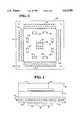
- FIG. 3shows a top level view of the power interface adapter 30 of the present invention.
- This power interface adapter(PIA) is fabricated using a double-sided printed circuit board.
- the PIA 30may also be fabricated as a multi-layer PCB.
- the additional internal voltage planesallow for distribution of multiple supply voltages as required per the device specification.
- PCB length, width and material thickness dimensionswill vary with the type of device socket 14, with the length and width dimensions generally being approximately equal to the length and width of the particular device socket, and the material thickness dimension to be determined based on the length of the device socket pins.
- the PIAhas a central region, indicated at 32, which comprises a plurality of plated conduits 34 through which the power interconnect pins 22 pass (as shown in FIG. 4).
- the PIAalso has a plurality of socket interface regions 36 around its periphery. These regions 36 have a plurality of plated conduits 42 through which socket pins 24 pass.
- the PIAhas a plurality of de-coupling capacitors 38 soldered thereon. These de-coupling capacitors provide supply voltage noise filtering for the integrated circuit package 20.
- the use of the PIA PCBprovides a platform which enables de-coupling capacitors to be located proximate to the device socket 14 power pins of the integrated circuit 20. This method of capacitor de-coupling for Universal burn-in board designs results in a marked improvement over existing supply voltage de-coupling techniques.
- the PIAhas mounting holes 40 at each corner, for mechanically mounting the PIA to the burn-in board sub-system.
- the completed burn-in board assemblyis shown for a single device socket location. It should be understood that there are a plurality of PIA 30 printed circuit boards used in conjunction with a single BIB, with each PIA being located at a particular device socket 14 location shown in FIG. 1.
- the PIA 30connects to the device socket pins 24 and power interconnect pins 22 located on the solder side of the burn-in board 12.
- the PIAslips over the plurality of pins 24 and 22, with these pins passing through plated conduits located within regions 32 and 36 of the PIA (such regions being shown in FIG. 3).
- the power interconnect pins 22 and device socket pins 24are preferably soldered to the PIA 30, although other methods of electrical interconnection are possible.
- An optional nylon spacer 44mechanically separates the PIA 30 from the burn-in board 12.
- a hinged or snap-in socket cap 46may optionally be included on top of the device socket 14. This socket cap is opened by lifting up lip 48 in order to insert an electrical component or integrated circuit device 20 (shown in phantom as inside the socket cap 46).
- supply voltagesare connected from the edge connector 10 of the burn-in board 12 to power interconnect pins 22.
- Power transfer to the PIAis accomplished via these multiple power interconnect pins 22, which provide VDD and VSS voltage connections to the power planes of the PIA (other additional voltages could similarly be provided to additional power planes in a multi-layer PCB).
- These voltage planesallow for distribution of the respective voltages to the required device socket pins 24.
- a PIA similar to the one in FIG. 3has been cut away.
- the thickness of the PIA in FIG. 5has been exaggerated to better show the internal voltage planes of the PIA.
- Power interconnect pins 22, which are centrally located at 32 on the top surface of PIA 30,receive supply voltages from the burn-in board.
- a first supply voltage VDDis connected from pins 54 and 60 down into an internal voltage plane 66 of the PIA.
- a second supply voltage VSSis connected from pins 56 and 58 down into an internal voltage plane 68 of the PIA.
- Internal voltage plane 66is connected to device socket pins 50 and 62
- internal voltage plane 68is connected to device socket pins 52 and 64.
- internal vias known in the artisolate pins 52, 56, 58, and 64 from the first internal voltage plane 66.
- device socket pins 24are electrically connected to device 20.
- device socket pins 50 and 62provide a first supply voltage such as VDD to device 20 via socket 14
- socket pins 52 and 64provide a second supply voltage such as VSS to device 20 via device socket 14.
- the remaining socket pins 36could either be signal pins for input and output signals to the device 20, or they could be connected to one or more of the other power interconnect pins 22 within area 32 of FIG. 5.
- FIG. 6shows the overall burn-in system 70, with an environmental chamber 72 having a burn-in socket 74.
- a cable 76is coupled between the burn-in socket and burn-in board.
- the burn-in boardis placed in the environmental chamber in order to subject the electrical devices on the burn-in board to environmental stress.
- a power supply voltage(as originally provided by a burn-in fixture) travels from the burn-in board edge connector 10, via a wiring conductor on the burn-in board 12, to a power interconnect pin 22.
- This voltage on the power interconnect pin 22is connected to the PIA at the point where the power interconnect pin passes through plated conduit 34 of the PIA.
- the PIAconnects the particular supply voltage that exists on the interconnect pin 22, via a power plane, to the desired socket pin 24.
- This socket pinwhich is electrically connected to the device socket 14, provides the supply voltage to the device 20 being burned-in.
- the PIAroutes supply voltages received from the power interconnect pins 22 to particular socket pins 24, as dictated by the location of the power pins for a particular device 14. If a different type or family of device has different locations for its power pins, then a different PIA would be required, with the PIA printed circuit board being fabricated to route the respective voltages to the appropriate power pins for the particular type or family of device.
- the particular PIA configuration of FIG. 5is but one of many possible supply voltage routing configurations. The requirements for the particular voltage supply routing, and the number of internal voltage planes needed for the PIA, are dictated by the particular device specification.
- a burn-in boardis to contain only a single type or family of device, where each device on the board has the same power pin locations, it is also possible to have a single, large PIA that is wired to route power for each of the devices. It would also be possible to have a PIA board that provides power supply voltage routing to a plurality of dissimilar types of devices. However, this is not the preferred method or system, due to the PIA's highly customized nature (and hence limited reusability when other types/configurations of devices are to burned-in).
Landscapes
- Engineering & Computer Science (AREA)
- Physics & Mathematics (AREA)
- General Physics & Mathematics (AREA)
- Environmental & Geological Engineering (AREA)
- Computer Hardware Design (AREA)
- Microelectronics & Electronic Packaging (AREA)
- General Engineering & Computer Science (AREA)
- Testing Of Individual Semiconductor Devices (AREA)
Abstract
Description
Claims (4)
Priority Applications (1)
| Application Number | Priority Date | Filing Date | Title |
|---|---|---|---|
| US08/614,925US5672981A (en) | 1994-09-16 | 1996-03-11 | Universal power interface adapter for burn-in board |
Applications Claiming Priority (2)
| Application Number | Priority Date | Filing Date | Title |
|---|---|---|---|
| US30806394A | 1994-09-16 | 1994-09-16 | |
| US08/614,925US5672981A (en) | 1994-09-16 | 1996-03-11 | Universal power interface adapter for burn-in board |
Related Parent Applications (1)
| Application Number | Title | Priority Date | Filing Date |
|---|---|---|---|
| US30806394AContinuation | 1994-09-16 | 1994-09-16 |
Publications (1)
| Publication Number | Publication Date |
|---|---|
| US5672981Atrue US5672981A (en) | 1997-09-30 |
Family
ID=23192388
Family Applications (1)
| Application Number | Title | Priority Date | Filing Date |
|---|---|---|---|
| US08/614,925Expired - LifetimeUS5672981A (en) | 1994-09-16 | 1996-03-11 | Universal power interface adapter for burn-in board |
Country Status (1)
| Country | Link |
|---|---|
| US (1) | US5672981A (en) |
Cited By (22)
| Publication number | Priority date | Publication date | Assignee | Title |
|---|---|---|---|---|
| EP0926505A1 (en)* | 1997-12-27 | 1999-06-30 | Franco Engeli | A device with removable configuration boards for testing integrated circuits |
| US6119255A (en)* | 1998-01-21 | 2000-09-12 | Micron Technology, Inc. | Testing system for evaluating integrated circuits, a burn-in testing system, and a method for testing an integrated circuit |
| US6150829A (en)* | 1999-04-05 | 2000-11-21 | Qualitau, Inc | Three-dimensional programmable connector |
| US6161205A (en)* | 1992-11-20 | 2000-12-12 | Micron Technology, Inc. | Testing and burn-in of IC chips using radio frequency transmission |
| US6175241B1 (en)* | 1999-02-19 | 2001-01-16 | Micron Technology, Inc. | Test carrier with decoupling capacitors for testing semiconductor components |
| US6218850B1 (en)* | 1999-04-22 | 2001-04-17 | United Microelectronics Corp. | Apparatus for selecting high-reliability integrated circuits |
| US6347946B1 (en)* | 2000-11-08 | 2002-02-19 | Intel Corporation | Pin grid array socket |
| US6407567B1 (en)* | 2000-06-29 | 2002-06-18 | Advanced Micro Devices | IC Device burn-in method and apparatus |
| US6472895B2 (en)* | 2000-12-06 | 2002-10-29 | Advanced Micro Devices, Inc. | Method and system for adapting burn-in boards to multiple burn-in systems |
| US6566899B2 (en)* | 2000-03-28 | 2003-05-20 | Kabushiki Kaisha Toshiba | Tester for semiconductor device |
| US6597190B2 (en)* | 2000-09-29 | 2003-07-22 | Intel Corporation | Method and apparatus for testing electronic devices |
| US20030197521A1 (en)* | 2002-04-17 | 2003-10-23 | Eagle Test Systems Inc. | Interface adapter for automatic test systems |
| US6667561B2 (en)* | 2002-03-13 | 2003-12-23 | Globespanvirata, Incorporated | Integrated circuit capable of operating in multiple orientations |
| US6698091B1 (en)* | 2000-12-29 | 2004-03-02 | Cisco Technology, Inc. | Method and apparatus for coupling circuit boards |
| US20050098778A1 (en)* | 2003-01-21 | 2005-05-12 | Renesas Technology Corp. | Burn-in test adapter and burn-in test apparatus |
| US20050116223A1 (en)* | 2003-11-27 | 2005-06-02 | Kenichi Ol | Burn-in substrate and burn-in device |
| CN1298038C (en)* | 2003-04-18 | 2007-01-31 | 索尼株式会社 | Semiconductor device |
| US20070126453A1 (en)* | 2005-11-14 | 2007-06-07 | Kim Sung B | Apparatus for testing a semiconductor device |
| US7808367B2 (en) | 1999-08-09 | 2010-10-05 | Round Rock Research, Llc | RFID material tracking method and apparatus |
| CN102123560A (en)* | 2011-03-01 | 2011-07-13 | 梅州博敏电子有限公司 | Embedded strong-current high-power PCB (Printed Circuit Board) and manufacturing method thereof |
| USRE42872E1 (en) | 1992-11-20 | 2011-10-25 | Round Rock Research, Llc | Method and apparatus for communicating with RFID devices coupled to a roll of flexible material |
| TWI705250B (en)* | 2019-07-17 | 2020-09-21 | 美商第一檢測有限公司 | Chip testing device |
Citations (23)
| Publication number | Priority date | Publication date | Assignee | Title |
|---|---|---|---|---|
| US3963986A (en)* | 1975-02-10 | 1976-06-15 | International Business Machines Corporation | Programmable interface contactor structure |
| US4145620A (en)* | 1977-10-05 | 1979-03-20 | Serel Corporation | Modular dynamic burn-in apparatus |
| US4417204A (en)* | 1980-04-03 | 1983-11-22 | Luther & Maelzer Gmbh | Printed circuit board tester and adapter with memory |
| US4542341A (en)* | 1982-01-04 | 1985-09-17 | Artronics Corporation | Electronic burn-in system |
| US4583042A (en)* | 1983-04-18 | 1986-04-15 | The Boeing Company | Capacitive circuit board testing system and method using a conductive pliant elastomeric reference plane |
| US4668041A (en)* | 1985-04-19 | 1987-05-26 | Intel Corporation | Low noise test contacts for pin grid array |
| US4747784A (en)* | 1986-05-16 | 1988-05-31 | Daymarc Corporation | Contactor for integrated circuits |
| US4926117A (en)* | 1988-05-02 | 1990-05-15 | Micron Technology, Inc. | Burn-in board having discrete test capability |
| US4933635A (en)* | 1988-12-22 | 1990-06-12 | International Business Machines Corporation | In-line process monitors for thin film wiring |
| US4950980A (en)* | 1988-07-29 | 1990-08-21 | Pfaff Wayne | Test socket for electronic device packages |
| US5068602A (en)* | 1990-09-07 | 1991-11-26 | Tektronix, Inc. | DUT board for a semiconductor device tester having a reconfigurable coaxial interconnect grid and method of using same |
| US5101149A (en)* | 1989-07-18 | 1992-03-31 | National Semiconductor Corporation | Modifiable IC board |
| US5132613A (en)* | 1990-11-30 | 1992-07-21 | International Business Machines Corporation | Low inductance side mount decoupling test structure |
| US5136471A (en)* | 1987-02-26 | 1992-08-04 | Nec Corporation | Laminate wiring board |
| US5144228A (en)* | 1991-04-23 | 1992-09-01 | International Business Machines Corporation | Probe interface assembly |
| US5157829A (en)* | 1990-10-02 | 1992-10-27 | Outboard Marine Corporation | Method of burn-in testing of circuitry |
| US5166605A (en)* | 1991-08-02 | 1992-11-24 | General Electric Company | Controlled impedance test fixture for planar electronic device |
| US5247248A (en)* | 1991-02-18 | 1993-09-21 | Sharp Kabushiki Kaisha | Burn-in apparatus and method of use thereof |
| US5258648A (en)* | 1991-06-27 | 1993-11-02 | Motorola, Inc. | Composite flip chip semiconductor device with an interposer having test contacts formed along its periphery |
| US5262719A (en)* | 1991-09-19 | 1993-11-16 | International Business Machines Corporation | Test structure for multi-layer, thin-film modules |
| US5270641A (en)* | 1992-01-22 | 1993-12-14 | Everett Charles Technologies, Inc. | Dual side access test fixture |
| US5367436A (en)* | 1992-03-11 | 1994-11-22 | Nec Corporation | Probe terminating apparatus for an in-circuit emulator |
| US5477160A (en)* | 1992-08-12 | 1995-12-19 | Fujitsu Limited | Module test card |
- 1996
- 1996-03-11USUS08/614,925patent/US5672981A/ennot_activeExpired - Lifetime
Patent Citations (23)
| Publication number | Priority date | Publication date | Assignee | Title |
|---|---|---|---|---|
| US3963986A (en)* | 1975-02-10 | 1976-06-15 | International Business Machines Corporation | Programmable interface contactor structure |
| US4145620A (en)* | 1977-10-05 | 1979-03-20 | Serel Corporation | Modular dynamic burn-in apparatus |
| US4417204A (en)* | 1980-04-03 | 1983-11-22 | Luther & Maelzer Gmbh | Printed circuit board tester and adapter with memory |
| US4542341A (en)* | 1982-01-04 | 1985-09-17 | Artronics Corporation | Electronic burn-in system |
| US4583042A (en)* | 1983-04-18 | 1986-04-15 | The Boeing Company | Capacitive circuit board testing system and method using a conductive pliant elastomeric reference plane |
| US4668041A (en)* | 1985-04-19 | 1987-05-26 | Intel Corporation | Low noise test contacts for pin grid array |
| US4747784A (en)* | 1986-05-16 | 1988-05-31 | Daymarc Corporation | Contactor for integrated circuits |
| US5136471A (en)* | 1987-02-26 | 1992-08-04 | Nec Corporation | Laminate wiring board |
| US4926117A (en)* | 1988-05-02 | 1990-05-15 | Micron Technology, Inc. | Burn-in board having discrete test capability |
| US4950980A (en)* | 1988-07-29 | 1990-08-21 | Pfaff Wayne | Test socket for electronic device packages |
| US4933635A (en)* | 1988-12-22 | 1990-06-12 | International Business Machines Corporation | In-line process monitors for thin film wiring |
| US5101149A (en)* | 1989-07-18 | 1992-03-31 | National Semiconductor Corporation | Modifiable IC board |
| US5068602A (en)* | 1990-09-07 | 1991-11-26 | Tektronix, Inc. | DUT board for a semiconductor device tester having a reconfigurable coaxial interconnect grid and method of using same |
| US5157829A (en)* | 1990-10-02 | 1992-10-27 | Outboard Marine Corporation | Method of burn-in testing of circuitry |
| US5132613A (en)* | 1990-11-30 | 1992-07-21 | International Business Machines Corporation | Low inductance side mount decoupling test structure |
| US5247248A (en)* | 1991-02-18 | 1993-09-21 | Sharp Kabushiki Kaisha | Burn-in apparatus and method of use thereof |
| US5144228A (en)* | 1991-04-23 | 1992-09-01 | International Business Machines Corporation | Probe interface assembly |
| US5258648A (en)* | 1991-06-27 | 1993-11-02 | Motorola, Inc. | Composite flip chip semiconductor device with an interposer having test contacts formed along its periphery |
| US5166605A (en)* | 1991-08-02 | 1992-11-24 | General Electric Company | Controlled impedance test fixture for planar electronic device |
| US5262719A (en)* | 1991-09-19 | 1993-11-16 | International Business Machines Corporation | Test structure for multi-layer, thin-film modules |
| US5270641A (en)* | 1992-01-22 | 1993-12-14 | Everett Charles Technologies, Inc. | Dual side access test fixture |
| US5367436A (en)* | 1992-03-11 | 1994-11-22 | Nec Corporation | Probe terminating apparatus for an in-circuit emulator |
| US5477160A (en)* | 1992-08-12 | 1995-12-19 | Fujitsu Limited | Module test card |
Cited By (41)
| Publication number | Priority date | Publication date | Assignee | Title |
|---|---|---|---|---|
| US6357025B1 (en) | 1992-11-20 | 2002-03-12 | Micron Technology, Inc. | Testing and burn-in of IC chips using radio frequency transmission |
| US6161205A (en)* | 1992-11-20 | 2000-12-12 | Micron Technology, Inc. | Testing and burn-in of IC chips using radio frequency transmission |
| USRE42872E1 (en) | 1992-11-20 | 2011-10-25 | Round Rock Research, Llc | Method and apparatus for communicating with RFID devices coupled to a roll of flexible material |
| EP0926505A1 (en)* | 1997-12-27 | 1999-06-30 | Franco Engeli | A device with removable configuration boards for testing integrated circuits |
| US6119255A (en)* | 1998-01-21 | 2000-09-12 | Micron Technology, Inc. | Testing system for evaluating integrated circuits, a burn-in testing system, and a method for testing an integrated circuit |
| US6640323B2 (en) | 1998-01-21 | 2003-10-28 | Micron Technology, Inc. | Testing system for evaluating integrated circuits, a testing system, and a method for testing an integrated circuit |
| US6189120B1 (en) | 1998-01-21 | 2001-02-13 | Micron Technology, Inc. | Testing system for evaluating integrated circuits, a burn-in testing system, and a method for testing an integrated circuit |
| US6484279B2 (en) | 1998-01-21 | 2002-11-19 | Micron Technology, Inc. | Testing system for evaluating integrated circuits, a testing system, and a method for testing an integrated circuit |
| US6349396B2 (en) | 1998-01-21 | 2002-02-19 | Micron Technology, Inc. | Testing system for evaluating integrated circuits, a burn-in testing system, and a method for testing an integrated circuit |
| US6175241B1 (en)* | 1999-02-19 | 2001-01-16 | Micron Technology, Inc. | Test carrier with decoupling capacitors for testing semiconductor components |
| US6396292B2 (en) | 1999-02-19 | 2002-05-28 | Micron Technology, Inc. | Test carrier with decoupling capacitors for testing semiconductor components |
| US6150829A (en)* | 1999-04-05 | 2000-11-21 | Qualitau, Inc | Three-dimensional programmable connector |
| US6218850B1 (en)* | 1999-04-22 | 2001-04-17 | United Microelectronics Corp. | Apparatus for selecting high-reliability integrated circuits |
| US7808367B2 (en) | 1999-08-09 | 2010-10-05 | Round Rock Research, Llc | RFID material tracking method and apparatus |
| US8125316B2 (en) | 1999-08-09 | 2012-02-28 | Round Rock Research, Llc | RFID material tracking method and apparatus |
| US8378789B2 (en) | 1999-08-09 | 2013-02-19 | Round Rock Research, Llc | RFID material tracking method and apparatus |
| US8269605B2 (en) | 1999-08-09 | 2012-09-18 | Round Rock Research, Llc | RFID material tracking method and apparatus |
| US6566899B2 (en)* | 2000-03-28 | 2003-05-20 | Kabushiki Kaisha Toshiba | Tester for semiconductor device |
| US6407567B1 (en)* | 2000-06-29 | 2002-06-18 | Advanced Micro Devices | IC Device burn-in method and apparatus |
| US20030206033A1 (en)* | 2000-09-29 | 2003-11-06 | Chan Kok Hong | Method and apparatus for testing electronic devices |
| US6885207B2 (en) | 2000-09-29 | 2005-04-26 | Intel Corporation | Method and apparatus for testing electronic devices |
| US6597190B2 (en)* | 2000-09-29 | 2003-07-22 | Intel Corporation | Method and apparatus for testing electronic devices |
| US6347946B1 (en)* | 2000-11-08 | 2002-02-19 | Intel Corporation | Pin grid array socket |
| US6472895B2 (en)* | 2000-12-06 | 2002-10-29 | Advanced Micro Devices, Inc. | Method and system for adapting burn-in boards to multiple burn-in systems |
| US6698091B1 (en)* | 2000-12-29 | 2004-03-02 | Cisco Technology, Inc. | Method and apparatus for coupling circuit boards |
| CN100351633C (en)* | 2002-02-11 | 2007-11-28 | 英特尔公司 | Method and apparatus for testing electronic devices |
| US6667561B2 (en)* | 2002-03-13 | 2003-12-23 | Globespanvirata, Incorporated | Integrated circuit capable of operating in multiple orientations |
| US6770493B2 (en) | 2002-03-13 | 2004-08-03 | Globespanvirata, Incorporated | Integrated circuit package capable of operating in multiple orientations |
| US20040084783A1 (en)* | 2002-03-13 | 2004-05-06 | Globespan Virata Inc. | Integrated circuit package capable of operating in multiple orientations |
| US6759842B2 (en)* | 2002-04-17 | 2004-07-06 | Eagle Test Systems, Inc. | Interface adapter for automatic test systems |
| US20030197521A1 (en)* | 2002-04-17 | 2003-10-23 | Eagle Test Systems Inc. | Interface adapter for automatic test systems |
| US20050146337A1 (en)* | 2003-01-21 | 2005-07-07 | Renesas Technology Corp. | Method of manufacturing and testing semiconductor device using assembly substrate |
| US20050098778A1 (en)* | 2003-01-21 | 2005-05-12 | Renesas Technology Corp. | Burn-in test adapter and burn-in test apparatus |
| CN1298038C (en)* | 2003-04-18 | 2007-01-31 | 索尼株式会社 | Semiconductor device |
| US7199598B2 (en)* | 2003-11-27 | 2007-04-03 | Espec Corp. | Burn-in substrate for semiconductor devices |
| US20050116223A1 (en)* | 2003-11-27 | 2005-06-02 | Kenichi Ol | Burn-in substrate and burn-in device |
| US20070126453A1 (en)* | 2005-11-14 | 2007-06-07 | Kim Sung B | Apparatus for testing a semiconductor device |
| US7535244B2 (en)* | 2005-11-14 | 2009-05-19 | Dongbu Hitek Co., Ltd. | Apparatus for testing a semiconductor device |
| CN102123560A (en)* | 2011-03-01 | 2011-07-13 | 梅州博敏电子有限公司 | Embedded strong-current high-power PCB (Printed Circuit Board) and manufacturing method thereof |
| CN102123560B (en)* | 2011-03-01 | 2012-10-03 | 博敏电子股份有限公司 | Embedded strong-current high-power PCB (Printed Circuit Board) and manufacturing method thereof |
| TWI705250B (en)* | 2019-07-17 | 2020-09-21 | 美商第一檢測有限公司 | Chip testing device |
Similar Documents
| Publication | Publication Date | Title |
|---|---|---|
| US5672981A (en) | Universal power interface adapter for burn-in board | |
| US6911835B2 (en) | High performance probe system | |
| US7928754B2 (en) | Wafer level burn-in and electrical test system and method | |
| US6462570B1 (en) | Breakout board using blind vias to eliminate stubs | |
| US7443181B2 (en) | High performance probe system | |
| US5946546A (en) | Chip burn-in and test structure and method | |
| US4772936A (en) | Pretestable double-sided tab design | |
| US5859538A (en) | Method and apparatus for connecting a ball grid array device to a test instrument to facilitate the monitoring of individual signals or the interruption of individual signals or both | |
| US6392428B1 (en) | Wafer level interposer | |
| US4862076A (en) | Test point adapter for chip carrier sockets | |
| US20060006892A1 (en) | Flexible test head internal interface | |
| JP2004523908A (en) | Adapters for plastic leaded chip carriers (PLCC) and other surface mount technology (SMT) chip carriers | |
| WO2004040325A1 (en) | Connection unit, board mounting device to be measured, probe card, and device interface unit | |
| JPH06213938A (en) | Connecting device | |
| US6018462A (en) | Multi-tip module | |
| US5383269A (en) | Method of making three dimensional integrated circuit interconnect module | |
| JPH07244114A (en) | Semiconductor device tester | |
| US7388424B2 (en) | Apparatus for providing a high frequency loop back with a DC path for a parametric test | |
| US6181146B1 (en) | Burn-in board | |
| US5243498A (en) | Multi-chip semiconductor module and method for making and testing | |
| US6507205B1 (en) | Load board with matrix card for interfacing to test device | |
| KR20010030217A (en) | Multichip module packaging process for known good die burn-in | |
| US6265952B1 (en) | Adapter for surface mounted devices | |
| US4514022A (en) | Probe cable assemblies | |
| JP3070437U (en) | Semiconductor test equipment |
Legal Events
| Date | Code | Title | Description |
|---|---|---|---|
| STCF | Information on status: patent grant | Free format text:PATENTED CASE | |
| AS | Assignment | Owner name:SYMBIOS, INC ., COLORADO Free format text:CHANGE OF NAME;ASSIGNOR:SYMBIOS LOGIC INC.;REEL/FRAME:009089/0936 Effective date:19971210 | |
| AS | Assignment | Owner name:LEHMAN COMMERCIAL PAPER INC., AS ADMINISTRATIVE AG Free format text:SECURITY AGREEMENT;ASSIGNORS:HYUNDAI ELECTRONICS AMERICA, A CORP. OF CALIFORNIA;SYMBIOS, INC., A CORP. OF DELAWARE;REEL/FRAME:009396/0441 Effective date:19980226 | |
| AS | Assignment | Owner name:HYUNDAI ELECTRONICS AMERICA, CALIFORNIA Free format text:TERMINATION AND LICENSE AGREEMENT;ASSIGNOR:SYMBIOS, INC.;REEL/FRAME:009596/0539 Effective date:19980806 | |
| FEPP | Fee payment procedure | Free format text:PAYOR NUMBER ASSIGNED (ORIGINAL EVENT CODE: ASPN); ENTITY STATUS OF PATENT OWNER: LARGE ENTITY | |
| FPAY | Fee payment | Year of fee payment:4 | |
| AS | Assignment | Owner name:HYNIX SEMICONDUCTOR AMERICA INC., CALIFORNIA Free format text:CHANGE OF NAME;ASSIGNOR:HYUNDAI ELECTRONICS AMERICA;REEL/FRAME:015246/0599 Effective date:20010412 Owner name:HYNIX SEMICONDUCTOR INC., KOREA, REPUBLIC OF Free format text:ASSIGNMENT OF ASSIGNORS INTEREST;ASSIGNOR:HYNIX SEMICONDUCTOR AMERICA, INC.;REEL/FRAME:015279/0556 Effective date:20040920 | |
| AS | Assignment | Owner name:MAGNACHIP SEMICONDUCTOR, LTD., KOREA, REPUBLIC OF Free format text:ASSIGNMENT OF ASSIGNORS INTEREST;ASSIGNOR:HYNIX SEMICONDUCTOR, INC.;REEL/FRAME:016216/0649 Effective date:20041004 | |
| FPAY | Fee payment | Year of fee payment:8 | |
| AS | Assignment | Owner name:SYMBIOS, INC., COLORADO Free format text:RELEASE OF SECURITY INTEREST;ASSIGNOR:LEHMAN COMMERICAL PAPER INC.;REEL/FRAME:016602/0895 Effective date:20050107 Owner name:HYUNDAI ELECTRONICS AMERICA, CALIFORNIA Free format text:RELEASE OF SECURITY INTEREST;ASSIGNOR:LEHMAN COMMERICAL PAPER INC.;REEL/FRAME:016602/0895 Effective date:20050107 | |
| AS | Assignment | Owner name:TAIWAN SEMICONDUCTOR MANUFACTURING CO., LTD., TAIW Free format text:ASSIGNMENT OF ASSIGNORS INTEREST;ASSIGNORS:NCR CORPORATION;MAGNACHIP SEMICONDUCTOR, LTD.;REEL/FRAME:021398/0702;SIGNING DATES FROM 20071114 TO 20071115 | |
| FPAY | Fee payment | Year of fee payment:12 |