US5672816A - Large stage system for scanning probe microscopes and other instruments - Google Patents
Large stage system for scanning probe microscopes and other instrumentsDownload PDFInfo
- Publication number
- US5672816A US5672816AUS08/448,004US44800495AUS5672816AUS 5672816 AUS5672816 AUS 5672816AUS 44800495 AUS44800495 AUS 44800495AUS 5672816 AUS5672816 AUS 5672816A
- Authority
- US
- United States
- Prior art keywords
- probe
- sample
- reflective surface
- stage
- scanning
- Prior art date
- Legal status (The legal status is an assumption and is not a legal conclusion. Google has not performed a legal analysis and makes no representation as to the accuracy of the status listed.)
- Expired - Lifetime
Links
Images


Classifications
- G—PHYSICS
- G01—MEASURING; TESTING
- G01Q—SCANNING-PROBE TECHNIQUES OR APPARATUS; APPLICATIONS OF SCANNING-PROBE TECHNIQUES, e.g. SCANNING PROBE MICROSCOPY [SPM]
- G01Q10/00—Scanning or positioning arrangements, i.e. arrangements for actively controlling the movement or position of the probe
- G01Q10/02—Coarse scanning or positioning
- G—PHYSICS
- G01—MEASURING; TESTING
- G01Q—SCANNING-PROBE TECHNIQUES OR APPARATUS; APPLICATIONS OF SCANNING-PROBE TECHNIQUES, e.g. SCANNING PROBE MICROSCOPY [SPM]
- G01Q30/00—Auxiliary means serving to assist or improve the scanning probe techniques or apparatus, e.g. display or data processing devices
- G01Q30/02—Non-SPM analysing devices, e.g. SEM [Scanning Electron Microscope], spectrometer or optical microscope
- G01Q30/025—Optical microscopes coupled with SPM
- G—PHYSICS
- G02—OPTICS
- G02B—OPTICAL ELEMENTS, SYSTEMS OR APPARATUS
- G02B21/00—Microscopes
- G02B21/0004—Microscopes specially adapted for specific applications
- G02B21/002—Scanning microscopes
- G—PHYSICS
- G02—OPTICS
- G02B—OPTICAL ELEMENTS, SYSTEMS OR APPARATUS
- G02B21/00—Microscopes
- G02B21/24—Base structure
- G02B21/26—Stages; Adjusting means therefor
- Y—GENERAL TAGGING OF NEW TECHNOLOGICAL DEVELOPMENTS; GENERAL TAGGING OF CROSS-SECTIONAL TECHNOLOGIES SPANNING OVER SEVERAL SECTIONS OF THE IPC; TECHNICAL SUBJECTS COVERED BY FORMER USPC CROSS-REFERENCE ART COLLECTIONS [XRACs] AND DIGESTS
- Y10—TECHNICAL SUBJECTS COVERED BY FORMER USPC
- Y10S—TECHNICAL SUBJECTS COVERED BY FORMER USPC CROSS-REFERENCE ART COLLECTIONS [XRACs] AND DIGESTS
- Y10S977/00—Nanotechnology
- Y10S977/84—Manufacture, treatment, or detection of nanostructure
- Y10S977/849—Manufacture, treatment, or detection of nanostructure with scanning probe
- Y10S977/86—Scanning probe structure
- Y10S977/868—Scanning probe structure with optical means
- Y10S977/87—Optical lever arm for reflecting light
Definitions
- the present inventionpertains to systems and methods for microscopically examining the surface of objects. More specifically, it pertains to the examination of large objects such as intact semiconductor wafers and lithographic photo-masks, using scanning probe microscopes such as scanning tunneling microscopes and atomic force microscopes.
- SPMscanning probe microscope
- Scanning probe microscopesinclude devices such as scanning force microscopes (SFMs), scanning tunneling microscopes (STMs), scanning acoustic microscopes, scanning capacitance microscopes, magnetic force microscopes, scanning thermal microscopes, scanning optical microscopes, and scanning ion-conductive microscopes.
- Probemeans the element of an SPM which rides on or over the surface of the sample and acts as the sensing point for surface interactions and may include the cantilever and tip, a chip from which the cantilever projects, and a plate on which the chip is mounted.
- SFMthe probe includes a flexible cantilever and a microscopic tip which projects from an end of the cantilever.
- the probeincludes a sharp metallic tip which is capable of sustaining a tunneling current with the surface of the sample. This current can be measured and maintained by means of sensitive actuators and amplifying electronics.
- the probeincludes a cantilever and tip which are conductive, and the cantilever deflection and the tunneling current are measured simultaneously.
- Cantilevermeans the portion of the probe of an SFM which deflects slightly in response to forces acting on the tip, allowing a deflection sensor to generate an error signal as the probe scans the surface of the sample.
- Tipin an SFM means the microscopic projection from one end of the cantilever which rides on or slightly above the surface of the sample.
- tiprefers to the metallic tip.
- SFMscanning Force Microscope
- An SFMmay operate in a contacting mode, in which the tip of the probe is in contact with the sample surface, or a non-contacting mode, in which the tip is maintained at a spacing of about 50 ⁇ or greater above the sample surface.
- the cantileverdeflects in response to electrostatic, magnetic, van der Waals or other forces between the tip and surface. In these cases, the deflection of the cantilever from which the tip projects is measured.
- STMscanning Tunneling Microscope
- SPMscanning Tunneling Microscope
- STMsare normally operated in a constant current mode, wherein changes in the tunneling current are detected as an error signal.
- a feedback loopuses this signal to send a correction signal to a transducer element to adjust the spacing between the probe and sample and thereby maintain a constant tunneling current.
- An STMmay also be operated in a constant height mode, wherein the probe is maintained at a constant height so that the probe-sample gap is not controlled, and variations in the tunneling current are detected.
- Kinematic mountingmeans a technique of removably mounting a rigid object relative to another rigid object so as to yield a very accurate, reproducible positioning of the objects with respect to each other.
- the position of the first objectis defined by six points of contact on the second. These six points must not over or under constrain the position of the first object.
- three balls on the first objectcontact a conical depression, a slot (or groove) and a flat contact zone, respectively, on the second object.
- the three ballsfit snugly within three slots formed at 120° angles to one another on the second object.
- kinematic mountingAccording to the principles of kinematic mounting, which are well known in the mechanical arts, six points of contact between the two objects are required to establish a kinematic mounting arrangement.
- the first ballmakes contact at three points on the conical surface (because of inherent surface imperfections, a continuous contact around the cone will not occur), two points in the slot, and one point on the flat surface, giving it a total of six contact points.
- each ballcontacts points on either side of the slot into which it fits.
- scanning probe microscopesincluding the scanning tunneling microscope and atomic force microscope
- Such microscopescan, in certain circumstances, resolve individual atoms on a surface and can map topographic variations on the sample with 0.1 nm vertical sensitivity or better.
- These microscopeshave found widespread application in academic and industrial research laboratories. The majority of systems constructed have been used for the examination of samples smaller than 25 mm in any one dimension. Samples of this size may conveniently be prepared and handled, and are commonly used in other types of optical and electron microscopes. In the semiconductor industry, for example, it is routine practice to fracture a wafer in order to microscopically examine a small fragment of it. The process is destructive and so the material examined is wasted.
- the mechanical linkage path between the microscope and the sampleis comprised of two separate bearing assemblies in the two translation stages assembled in series; vibrational or thermal instabilities or non-planarities or non-linearities of motion are additive for the two stages and produce a composite positioning error which can substantially degrade the performance or positioning accuracy of the microscope. It is the stability of this mechanical support path which determines the mechanical stability of the microscope and its ability to resolve fine structures as well as to image the same point on the object even when the instrument is subject to external physical sources of interference such as vibrations, temperature fluctuations, and the like.
- a key goalis to minimize the number of bearing stages between the sample and the microscope and to maximize the mechanical stability and strength of the complete support path whilst providing a means of precisely and accurately positioning the sample relative to the microscope.
- auxiliary optical microscopeis employed to locate the desired imaging location visually in the first place, so that the probe microscope tip can be correctly positioned over the sample.
- Such a systemis disclosed in application Ser. No. 07/850,677, filed Mar. 13, 1992, now U.S. Pat. No. 5,448,399.
- Video optical microscopescan scan images much faster than typical probe microscopes of the present generation, and so overall throughput is increased by this combination of techniques.
- the video imagemay be digitized so that the site selection process can be fully automatic using pattern recognition and other image analysis techniques.
- U.S. Pat. No. 4,999,494 to Elingsdescribes a scanning tunneling microscope system in which the microscope head is supported by feet which bear on the surface of the sample or on another surface which supports the sample.
- the probe microscopeis attached to motorized stage means which position the microscope head in a plane roughly parallel to the sample surface.
- the headis unconstrained in the vertical direction and can thus accommodate variations in the flatness of the support surface whilst remaining in contact with the surface.
- a limitation of this approachis that the translation speed of the stage and the ability of the stage to make the smallest incremental motions is limited by friction and stiction effects between the support feet and the translation surface, which effects are always present since the support feet are permanently in contact and supporting the weight of the probe microscope.
- a further limitation of the approachis that there may be wear to either the feet or to the sample or support surface as the sample is translated, since the surfaces are rubbing. For semiconductor applications, this is particularly undesirable since the particles thus generated can cause defects to appear on the circuits being inspected.
- the Koshiba arrangementis specifically designed to provide an elastic coupling between the movable stage and the base and to allow tilting of the movable stage. This is entirely unsuitable for an SPM.
- Optical detection as disclosed by Elingsrequires precise alignment of the cantilever with the illuminating laser beam; furthermore, the optical arrangement is bulky and reduces scanning fidelity. Finally the optical interferometer arrangement requires that the cantilever be deformed in order to satisfy an optical interference condition for correct operation, and this means that the force exerted by the tip on the sample may not be precisely selected in order to optimize imaging conditions.
- An article by G. L. Miller et al. in Rev. Scientific Instruments 62(3), March 1991, and an article by D. A. Grigg in Ultramicroscopy, May 1992describe an atomic force microscope in which capacitance displacement sensors are incorporated in order to detect tip deflections due to sample topography as well as to detect lateral deflections of the scanner. This has the distinct advantage that the detection system is purely electronic in nature, although the capacitance detector is bulky and complex; it may not be easily batch fabricated but requires external electronics in order to energize and process the detector signals.
- the cantileverdoes not have a monolithic probe tip mounted on the cantilever for scanning the surface of the sample.
- the tipmust be glued to the cantilever before use.
- the process describeddoes not achieve the economy of fabrication or simplicity of operation that is desired.
- a specific object of the inventionis to provide a translation stage coupled to a microscope and sample which links the two in a stable kinematic configuration whilst imaging is in progress, but which permits lateral translation of the microscope relative to the sample using a very low friction air bearing whilst the parts are in relative motion.
- very high mechanical stability and immunity to external vibrationsis achieved whilst the translation means is static, but whilst it is moving the reduced friction of the air bearing permits high speed motion, thereby reducing the effects of backlash and stiction which can limit positioning accuracy and precision with conventional stage systems.
- a bright-field oblique optical viewreceives a much greater amount of reflected light from the imaged object than a dark-field view, which receives mainly scattered light from the imaged object in the oblique optical view.
- a single translation stagemoves laterally on air bearings over a smoothly polished, highly planar base.
- the translation stageis free to move in any horizontal direction.
- the air bearingsare de-energized and a source of vacuum may be connected to the air bearings, thereby holding the translation stage tightly against the base. Since the air bearings are formed of rigid materials, the translation stage is held firmly in place so that highly delicate operations, such as the scanning of a sample with a scanning probe microscope, can be performed.
- pressurized airis supplied to the air bearings.
- the translation stagemay then be moved easily and precisely to a new position, which may be far removed from the original position, without countering the effects of stiction and friction.
- the scannere.g., a piezoelectric tube
- the scanneris mounted in the head of a scanning probe microscope. Accordingly, the scanner is forced to move only the fixed, limited mass of the probe and detection system, rather than the variable mass of the sample. This arrangement is particularly suitable for examining large samples.
- FIG. 1Aillustrates a block diagram of the computer control unit of an embodiment according to this invention.
- FIGS. 1B and 1Cillustrate side and top views, respectively, of a microscope head unit in accordance with this invention.
- FIG. 2illustrates a top view of the lateral translation units of the microscope.
- FIG. 3illustrates a horizontal cross-sectional view of the translation stage and guide.
- FIG. 4Aillustrates a perspective view of the translation stage and components thereof and a schematic view of the pressurized air and vacuum supply units.
- FIG. 4Billustrates a vertical cross-sectional view through the center of an air bearing.
- FIG. 5illustrates the construction of the adjustment hinge mechanisms for the roller bearing assemblies.
- FIG. 6Aillustrates a vertical cross-sectional view of the translation stage and guide taken through section A--A shown in FIG. 1C.
- FIG. 6Billustrates a vertical cross-sectional view of the translation stage and guide taken through section B--B shown in FIG. 1C.
- FIG. 7Aillustrates a side view of the microscope head, showing the TV system, taken from direction C shown in FIG. 1B.
- FIG. 7Billustrates a top view of the TV system, taken from direction D shown in FIG. 1B.
- FIG. 8Aillustrates a cross-sectional exploded view of the scanner.
- FIG. 8Billustrates the mounting of the fixture containing photodiodes on the piezoelectrical tube.
- FIG. 8Cillustrates the kinematic mounting of the scanner on the bracket.
- FIG. 8Dillustrates a bottom view of the probe.
- FIG. 8Eillustrates a perspective view of the probe and probe mount.
- FIG. 9illustrates a view of the shutter motor mechanism.
- FIGS. 10A, 10B, and 10Cillustrate side views of second, third and fourth embodiments of a translation stage according to the invention.
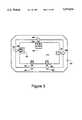
- FIGS. 1A and 1Billustrate the overall system schematically.
- a computer control unit 110 and a video display screen 111are used to control the operation of a microscope head unit 100 and to record and analyze data and images therefrom.
- Computer control unit 110includes interfacing circuitry for generating scanning and positioning signals to a probe microscope head 106, for controlling stage translation units 108 and 109, for controlling a sample stage 105 and a TV system 113, and for recording data from these various units. Images and data are displayed on video display screen 111, and a graphical user interface permits selection and control of the overall microscope operation. Details of the software control structure are specifically disclosed in U.S. application Ser. No. 07/851,560, now abandoned, and details the function of the controller are disclosed in U.S. Pat. No. 5,376,790.
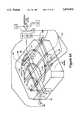
- Microscope head unit 100includes an external enclosure 103 which is designed to reflect or absorb external sources of vibrational or acoustic energy, as well as to maintain a uniform temperature within the enclosure. Typically, it may be fabricated from steel or polymer materials, and sound deadening materials may be laminated to its surfaces in order to optimize microscope performance.
- FIG. 1Cshows a top view of microscope head unit 100 in which external enclosure 103 has been omitted for clarity.
- a sample 104is introduced to the microscope head through an entry door 112 (FIG. 1B), either automatically by a robot or manually by an operator. Sample 104 is positioned on sample stage 105 and is captured thereon by holding means incorporated in stage 105, which holding means may be based upon mechanical fixtures, or by electrostatic magnetic or vacuum chucking, or by other means according to the type of sample and other considerations.
- Sample stage 105rests in static configuration on a surface 115 of a reference block 102 which has been ground to a precise contour.
- surface 115is ground flat to high precision, such that translation of sample stage 105 over surface 115 provides minimal motion of sample 104 with respect to probe microscope head 106 and TV system 113 in a direction perpendicular to surface 115.
- reference block 102may be fabricated from granite, which has excellent mechanical strength and thermal inertia, whilst it provides high damping of any vibrational energy coupled into it.
- Reference block 102may be 100 mm in thickness or more.
- Reference block 102is mounted on servo-vibration isolating units 101 which are mounted on a floor standing support table, 114. Combined servo-vibration isolation units 101 and floor-standing support table 114 are available for example from the Technical Manufacturing Company, Peabody, Mass.
- Sample stage 105may be translated in two axes by motor translation units 108 and 109 which operate under command from computer control unit 110. During translation, sample stage 105 may be partially or fully supported by an integral air-bearing mechanism such that there is negligible friction between sample stage 105 and surface 115.
- Probe microscope head 106 and TV system 113are rigidly mounted to a support structure 107, which is itself mounted rigidly on reference block 102.
- Support structure 107is designed to minimize the motion of the microscope head 106 and the TV system 113 with respect to reference support block 102. Typically, it may be constructed of materials which combine high strength with a low coefficient of thermal expansion as well as good acoustic damping characteristics. Materials such as granite or steel are suitable for this application. Support structure 107 is mounted to reference block 102 at three points around the perimeter of block 102 in order to ensure that the structure is optimally stable and has a high mechanical resonant frequency.
- support structure 107may be built from a steel I-beam girder of cross-sectional dimensions 100 mm ⁇ 100 mm with a web thickness of 2 cm and may be coupled to reference block 102 along its length by an additional structure welded to it, as illustrated in FIGS. 1B and 1C.
- Design of support structure 107follows conventional mechanical design principles.
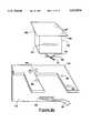
- FIG. 2illustrates top view of reference block 102 and sample translation systems 108 and 109.
- Lateral motion of a sample stage guide 219is guided by two linear track bearings, numbered 211 and 218, which are mounted orthogonal to one another.
- Bearings 211 and 218are selected for offering good linearity of motion coupled with a high resistance to mechanical and thermal fluctuations. Bearings 211 and 218 also provide high resistance to forces which could cause rotation, pitch and yaw or other deviations relative to the desired motion axis. Such bearings utilize a recirculating ball mechanism.
- Bearing 218is rigidly mounted to reference block 102.
- a slider 212is attached to two recirculating ball heads 231 and 232 which are freely movable along the length of bearing 218 with low friction. Two heads are used for this purpose since they provide enhanced stiffness against rotation of slider 212 about an axis perpendicular to surface 115.
- the position of slider 212 along bearing 218is controlled by a leadscrew 215 acting on a lead nut 214, which is in turn rigidly attached to slider 212.
- Leadscrew 215passes through a clearance hole bored in slider 212.
- Rotation of leadscrew 215is accomplished by a motor 216 driving through a coupler 213 and a thrust bearing 223, under instruction from computer control unit 110.
- Motor 216is rigidly attached to a support member 217, which is in turn rigidly attached to reference block 102.
- Bearing 211is rigidly attached to slider 212 at one end, whilst the other end of bearing 211 is cantilevered above reference surface 115.
- Means for stiffening bearing 211 in the vertical axismay be provided in order to increase the resonance frequency of the bearing to vertical oscillations and so minimize vibrational sensitivity.
- bearing 211may be coupled to reference block 102 in a manner which constrains motion of bearing 211 in a direction perpendicular to reference surface 115 yet leaves bearing 211 free to move in a direction parallel to the surface of reference block 102. Such may be accomplished by the addition of an extra roller or track bearing assembly placed at the free end of bearing 211, running parallel to and equivalent to bearing 218, or by equivalent means.
- Sample stage guide 219is attached to two or more of recirculating ball sliders 233 and 234, which are freely slidable along the length of bearing 211. As with slider 212, sample stage guide 219 is positioned along the length of bearing 211 by a leadscrew 210 and a lead nut 220, which is rigidly attached to sample stage guide 219. A clearance hole for leadscrew 210 is bored through sample stage guide 219. Leadscrew 210 is driven by a motor 209 acting through a coupler 221 and a thrust bearing 222. Motor 209 is rigidly mounted to slider 212 and receives drive signals from computer control unit 110.
- Motors 216 and 209may be chosen for desirable torque and speed characteristics and may be DC or stepping motors. Stepping motors are preferred since they provide an economical means of precisely positioning the sample stage 105 without the use of additional position sensors which would be required if DC motors were used. Motor drive circuitry and software must be properly designed such that the motors can perform at high frequency, in order to give the high translation speeds made possible by the low friction air-bearings employed in this design, yet provide a sufficiently small minimum step size for precise translational motion of the Sample. In particular the drive amplifier impedances and the acceleration and deceleration software routines must be carefully optimized, as will be evident to those skilled in the art. Also viscous damping systems may be coupled to the motor spindle such that transient performance is improved. Micro-stepping drives may provide a reduced minimum step size whilst permitting higher speed translation. Typically motors 209 and 216 translate at two inches per second maximum speed, with a minimum step size of 6microns.
- Limit switches 205, 206, 207 and 208serve to signal to computer control unit 110 when slider 212 or stage guide 219 has reached the limits of its travel in either direction and may be of mechanical or optical types.
- Leadscrews 215 and 210may be of ground steel with lead chosen to provide suitable speed of motion and step size of motion.
- Lead nuts 214 and 220are of the anti-backlash type and may use either spring preloading or be of the recirculating ball type for increased accuracy of motion.
- sample stage guide 219may thus be accurately controlled in two orthogonal directions by computer control unit 110.
- Sample stage 105is placed over sample stage guide 219 and is mechanically coupled to it such that the horizontal position of sample stage guide 219 kinematically defines the position of sample stage 105 on reference surface 115, whilst permitting free motion of sample stage 105 in a direction perpendicular to reference surface 115.
- FIG. 2illustrates five roller bearing assemblies 224, 225, 226, 227 and 228 whose centre elements are rigidly mounted, with outside elements freely rotatable, at five points around the edges of sample stage guide 219, with their rotational axes oriented horizontally.
- Bearings 224-228are of a ball race roller type with planar or radiused outer bearing surfaces.
- Bearings 226 and 228are rigidly coupled to sample stage guide 219 via adjustment hinge mechanisms 229 and 230 respectively. These mechanisms permit fine translational adjustment of the centre of rotation of the roller bearings in a direction parallel to surface 115 and orthogonal to the rotational axes of the respective roller bearings.
- FIG. 5illustrates the design of adjustment hinge mechanisms 229 and 230, which are identical.
- Hinge block 500is machined to be rigidly attached to sample stage guide 219 along rear surface 503.
- Roller bearing 226 or 228is mounted onto hinge block 500 as shown and is free to rotate.
- Hinge block 501is machined to a thin flexible hinge point along its length, point 501, such that the separation of bearing 226 from rear surface 503 can be adjusted by set screw 502 which is threaded into hinged portion 504 of hinged block 500.
- Other mechanisms for translation adjustment of roller bearings 226 and 228 with different force/displacement characteristicswill be clear to those skilled in the art and may be substituted for adjustment hinge mechanisms 229 and 230 where more constant preloading forces are desired.
- FIG. 3is a cross-sectional view of sample stage 105 and stage guide 219 through a section parallel to surface 115 at the height of the axles of roller bearings 224-228 and shows the manner in which sample stage guide 219 engages sample stage 105.
- Bearings 224, 225, 226, 227 and 228engage corresponding bearing surfaces 300, 301, 302, 303 and 304 respectively. These bearing surfaces should ideally be cylindrical, such that a cross section parallel to surface 115 is circular and so that there is a single point of contact between the bearings and their corresponding bearing surfaces. In some applications, it may be sufficient to provide flat bearing surfaces.
- Bearing surfaces 300-304are embedded into an interior surface of sample stage 105 such that sample stage 105 can freely translate in the vertical direction.
- Bearings 224, 225 and 226serve to constrain the motion of sample stage 105 in a horizontal direction orthogonal to bearing 211 as well as preventing rotation of sample stage 105 about an axis perpendicular to surface 115.
- Bearing 226may be adjusted in order to minimize play in this direction and establish appropriate loading on bearings 224, 225 and 226.
- Bearings 227 and 228constrain the motion of sample stage in a direction parallel to bearing 211, and the location of bearing 228 may be adjusted by hinge mechanism 230 in order to establish minimal play and appropriate loading on bearings 227 and 228.
- the location of sample stage 105 with respect to sample stage guide 219is kinematically defined in a plane parallel to reference surface 115.
- FIG. 4is a perspective view of the general configuration of three air bearings 401, 402 and 403, which rest on surface 115 when the air supply is switched off, but which raise the stage a few microns above the surface when compressed air is supplied to the three jets through fittings 404, 405 and 406 respectively; pipes bored into stage 105 conduct compressed air to the three air bearings.
- the air supply to fittings 404, 405 and 406is separately adjusted by air pressure regulators 407, 408 and 409, respectively, so that the stage floats evenly above surface 115, even if the mass loading of sample 104 and sample stage 105 is not evenly distributed on the three air bearings.
- the air supply to the regulators 407, 408 and 409is switched by a solenoid-driven switch valve 410 which operates under command from computer control unit 110.
- a typical motion sequenceinvolves first turning on the air bearings through valve 410 and waiting for the air bearings to rise. Then the motors 209 and 216 are used to translate the sample stage 105 to the required location. At that point, the air bearings are disengaged using valve 410.
- Servo-mechanisms for automatically regulating the height and tilt of stage 105, incorporating pressure or other types of proximity sensors and pressure controllerswill be apparent to those ordinarily skilled in the art.
- FIGS. 6A and 6Bshow a cross-sectional view through sample stage 105 and stage guide 219, illustrating the relationship of the various components which interact with sample stage 105, stage guide 219 and reference block 102.
- Air supply ductingwhich is bored into sample stage 105 in order to connect supply pipes is not shown for clarity. It is seen that the stage 105 is free to move in the vertical direction guided by bearings 227 and 228 as well as the bearings 224, 225 and 226.
- Air bearings 401, 402 and 403are machined separately to fit into sample stage 105 and are inset to their respective locations using a press.
- the top surface of sample stage 105is ground and polished precisely parallel to the contact plane of air bearings 401, 402 and 403, such that when the stage is translated on surface 115 the height of the top surface of stage 105 is invariant. This is advantageous since the surface height of a parallel-sided sample 104 thus remains constant even as it is translated, and a probe can be maintained in close proximity to the surface of sample 104 so the time spent recontacting the surface can be shortened.
- FIG. 4BA typical air bearing is illustrated in FIG. 4B as a cross section through air bearing 402 in a plane orthogonal to surface 115.
- An air bearing aperture 451provides a reactive force to sample stage 105 in a direction away from surface 115 roughly equal to the surface area of the aperture multiplied by the air pressure supplied to it via a bored pipe 452 and pipe fitting 405.
- Different sized apertures for the air bearingscan be employed to provide different degrees of floatation force according to the mass of sample 104 and sample stage 105.
- sample stage 105is built from a dense material, such as stainless steel, it is advantageous to machine a large air bearing area in order to exert the necessary lifting force at modest air supply pressure; when the combined mass of sample 104 and stage 105 is small then a smaller air emission surface area may be acceptable.
- a diameter of 1 cm for aperture 451may be suitable for a sample stage 105 made from stainless steel, whereas a diameter of only 5 mm may be suitable where the sample stage is constructed from aluminum; in both cases the stage floats with air inlet pressures of approximately 20-30 pounds per square inch.
- the design of air bearingsfollows conventional principles which are known to those skilled in the art.
- Air bearings 401, 402 and 403may be machined from stainless steel or other materials, and may have a single or multiple orifices in order to distribute the load. Furthermore, air bearings 401, 402 and 403 may have a pointed or spherical lower surfaces which contact surface 115 when the air bearings are de-energized, such that there are only three points of contact between sample stage 105 and surface 115, one at each air bearing. In this way, the mechanical stability of sample stage 105 with respect to tilt is assured since the three contact paints provide optimum stability and, combined with the kinematic interaction with stage guide 219, sample stage 105 is uniquely positioned with very high stability.
- FIG. 4Aalso shows surface details of sample stage 105.
- Sample stage 105includes a milled surface pattern 12 which is connected through internal ductwork and external piping 413 to a vacuum pump 411, such that when a sample 104 is placed on the stage 105, the vacuum thus created holds the sample to the stage with excellent stability.
- Vacuum vents of various shapesare provided such that semiconductor wafers and the like of different diameters can be so attached to sample stage 105.
- Vacuum valve 414controls the vacuum supply and may be either manually controlled or may receive computer control signals from controller 110.
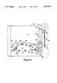
- FIG. 7Ashows the disposition of probe microscope head 106 on support structure 107 with respect to sample 104.
- the microscope head 106includes a probe 701 and means for scanning the probe over the sample surface, comprising a scanner assembly 703.
- Probe 701is kinematically, removably mounted on a probe mount 702, which in turn secured to scanner assembly 703.
- Microscope head 106also includes two optical microscopes, described below, for providing an on-axis view of the sample surface and an oblique view of the probe and the sample.
- TV system 113is also described below.
- a portion of microscope head 106is raised or lowered relative to both support structure 107 and sample translation stage 105 by means of a motor-driven, vertical translation stage 705.
- Vertical translation stage 705comprises a plate 761 mounted on a vertical slide rail 760.
- Slide rail 760is rigidly fixed to a vertical plate 762 which in turn is rigidly fixed to support structure 107.
- Stage 705thus can be raised or lowered relative to support structure 107.
- a bracket 704is rigidly fixed to vertical stage 705.
- Scanner assembly 703is kinematically, removably mounted onto this bracket.
- an objective lens 709, a lens 710, and mirrors 711 and 712are attached to bracket 704.
- the motion of vertical translation stage 705is controlled by a stepping motor 706 and a micrometer 707, under control of computer control unit 110.
- the drive shaft of stepping motor 706is axially connected via a flexible coupler to a pushing screw 706a which is threaded through a fixed nut 706b mounted on plate 762.
- Stepping motor 706slides on a slide rail 706c also mounted on plate 762 as pushing screw 706a advances or retreats through fixed nut 706b.
- Stage 705is biased against the tip of the pushing screw by a pair of springs 766 as well as by a fixture 767 rigidly fixed to stage 705.
- Springs 766are connected between stage 705 and plate 762.
- Fixture 767rigidly connects the body of stepping motor 706 to stage 705.
- Fixture 767also makes contact with the tip of pushing screw 706a, as shown in FIG. 7A.
- Springs 766 in combination with fixture 767provide means to maintain contact between the tip of the pushing screw and stage 705 at all times.
- springs 766provide means to reduce significantly backlash between pushing screw 706a and fixed nut 706b.
- stage 705is lowered or raised, respectively, relative to both support structure 107 and sample stage 105.
- Micrometer 707has a resolution of 80 turns per inch of travel.
- Limit switches 718 and 719are attached to plate 762 and signal to control unit 110 when stage 705 is at the limits of its travel.
- Stage 705thus provides for motion of probe 701 along an axis perpendicular to sample 104.
- Stage 705also provides for adjustment of the focus of objective lens 709, by lowering or raising the focal plane of lens 709 with respect to an imaged object.
- the components shown in FIG. 7Aalso form a video microscope system which selectively permits viewing of sample 104 at high magnification from a perpendicular direction above the sample using lens 709, or viewing of probe 701 and sample 104 at lower magnification at an oblique angle through lens 710.
- This dual facilityis very valuable in controlling the probe microscope since both the integrity of probe 701 and the location to be examined on sample 104 can conveniently be selected.
- TV system 113includes a color video camera 750, and a motorized zoom lens 751 as well as two mirrors 752 and 753 for directing light from an optical beam splitter 715 along a beam path 754.
- Motorized zoom lens 751may be a 60 mm-300 mm focal length motorized zoom lens, or other zoom lens combined with a motor, such as has been disclosed in application Ser. No. 07/850,677.
- Video camera 750, zoom lens 751 and mirrors 752 and 753are mounted on flat plates which are attached to support structure 107.
- high magnification microscope objective lens 709is attached to bracket 704, and provides a view of the surface of sample 104 from a roughly perpendicular direction.
- An image of sample 104is reflected by a beam splitter 715 towards TV system 113 such that an image of the sample may be viewed on monitor 111.
- Low magnification lens 710 and mirrors 711 and 712are attached to bracket 704 and thus can be raised or lowered via vertical translation stage 705.
- Lens 710is focused obliquely onto probe 701 and may be a 50 mm focal length bi-convex lens. Thus the surface of sample 104 comes into focus when probe 701 is in the proximity of sample 104.
- a mirror 713 and optical beam splitter 715are mounted on a vertical plate 770 attached to support structure 107.
- Mirrors 713,712 and 711serve to direct light from beam splitter 715 to lens 710 along a beam path 720 and to direct the image back along the same path, through beam splitter 715 and thus to TV system 113, causing an image to be seen on monitor 111 (FIG. 1).
- the probe 701should remain in focus over the entire travel of stage 705 since this permits visualization of the integrity of probe 701 at all times. This is accomplished by arranging that the lens 710 operate at infinite conjugate i.e., the lens 710 forms an image of the probe at infinity, by placing the imaged object one focal length in front of the lens, and also by ensuring that beam path 720 between mirrors 712 (mounted on bracket 704) and 713 (rigidly fixed to support structure 107) is parallel to the direction of motion of stage 705.
- Other equivalent means for ensuring that the probe remains in focuswill be obvious to those skilled in the art, including the provision of a second focusing mechanism to accomplish this task.
- Illumination for the two viewing systemsis provided from a single illuminating light bulb 717 via a condenser lens 716 and beam splitter 715.
- Beam splitter 715splits the illuminating light into two beams of roughly equal intensity.
- the first beamilluminates sample 104 through lens 709, in an arrangement commonly known in microscopy as Kohler illumination, which provides uniform spatial illumination.
- An on-axis image of sample 104is formed by lens 709 and directed towards TV system 113 by reflection from plate glass beam splitter 715.
- the video image of sample 104may be visualized on monitor 111.
- the second beam of illuminating lightis reflected by beam splitter 715 towards mirror 713, and serves to illuminate the oblique view through lens 710 via mirrors 713, 712 and 711.
- a shutter 722is mounted on the spindle of a motor 721 such that it may be rotated. Which view (on-axis or oblique) is visualized on monitor 111 is determined by the position of shutter 722, which selectively obscures one of the two images according to control signals from computer 110. Thus only one image is visualized at a time.
- FIG. 7Aillustrates the shutter 722 in position to block the on-axis view (through lens 709) such that the oblique view is visualized; if shutter 722 is rotated to position 714 (dashed lines) then the oblique view (through lens 710) is obscured and the on-axis view is visualized. Intermediate positions for shutter 714, or other arrangements, would permit simultaneous viewing of parts of both images.
- Bulb 717, lens 716 and motor 721are mounted on vertical plate 770 which is attached to support structure 107.
- Shutter 722is a bracket which is preferably coated to be optically absorbent, either by painting or anodizing it black, or by the use of black velvet material, as is commonly known in the art. Shutter 722 may also be angled with respect to the light beam in order to reflect energy away from beam splitter 715. Motor 721 may be any type of stepping motor for positioning objects rotationally, or the like.
- a mirror 723is attached to probe mount 702.
- Mirror 723is positioned and angled such that it reflects the lost illumination reflected by the sample and probe back along a reverse path so that the sample and probe are now illuminated in bright field conditions and the oblique view optical image is substantially improved.
- Mirror 723may be planar or may be curved for improved efficiency or to accommodate a wider range of probe and sample surface gradients.
- the angle, position, shape and size of mirror 723are dictated by the angle of the oblique view, and by the slope of the sample surface and by other factors, as will be clear to those skilled in the art.
- the direction of light from bulb 717 incident on the probecan be altered, using lenses and mirrors, so that the probe is illuminated from the opposite side of scanner assembly 703.
- the direction of illuminationis angled in such a way that specularly reflected light from the probe and sample follows the reciprocal path 720.
- scanner assembly 703may at least partially block this path of direct illumination. Means for overcoming this obstruction, for instance by directing light through an opening in the side of scanner assembly 703 and past the probe mount 702, may be somewhat cumbersome.
- Another alternative embodimentuses a light source positioned substantially beneath scanner assembly 703 so that sample and probe are illuminated from close range, for instance by an LED (light-emitting diode) or a fiber optic light source.
- a light sourcepositioned substantially beneath scanner assembly 703 so that sample and probe are illuminated from close range, for instance by an LED (light-emitting diode) or a fiber optic light source.
- This probe microscope systemconcerns minimizing the risk of collisions when inspecting objects with undulating topography.
- some raised portion of the sample 104may contact either probe 701 or objective lens 709 with the attendant risk of damage to those elements.
- lens 709may be struck by some raised portion of sample 104 distant from the probe location whilst the stage is in motion.
- probe 701may be struck by some raised portion of sample 104 when stage 105 is in motion.
- probe 701In order to minimize the risk of such collisions, it is advantageous to position probe 701 so that it is approximately at the mid-point of the working distance of objective lens 709, which is to say that when lens 709 is focused on a flat sample, probe 701 is separated from the sample 104 by half the distance that lens 709 is separated from the sample.
- a sample with a protrusion of height equal to the working distance divided by 2can only just strike probe 701 when the stage is in motion.
- the same size of sample protrusion(working distance divided by 2) can just strike lens 709.
- the height separation between probe 701 and the focal plane of lens 709may be reduced such that minimal time is spent in adjusting stage 705 when changing imaging mode from probe to optical viewing, and vice-versa.
- the sample 104must be loaded into the instrument. This is accomplished by first raising vertical translation stage 705 so that probe 701 is clear of any protrusions on sample stage 105, energizing the stage 105 air bearings and translating the stage to some convenient loading location under computer control. Having loaded the sample and secured it using the vacuum chuck or by other means, the stage may then be translated to place some portion of the sample beneath lens 709. Motor 706 is commanded to position vertical translation stage 705 such that lens 709 is focused onto the surface of the sample. At this time, probe 701 is clear of the sample surface since it is mounted above the focal plane of lens 709.
- sample 104can be translated laterally over surface 115 to select the field of view.
- the integrity of probe 701can be viewed using oblique lens 710.
- the stage 105can be commanded to translate a pre-programmed lateral displacement which causes the probe 701 to be above the selected region of sample 105.
- Air supply to air bearings 401-403 of stage 105can then be disconnected by valve 410 and vacuum pump 411 can be connected to air bearings 401-403 so that stage 105 is drawn firmly to surface 115 of block 102.
- Probe 701can then be lowered towards the sample surface for scanning, under computer control of vertical translation stage 705 through motor 706. During this sequence, probe 701 may be continuously examined using oblique viewing lens 710 since the image through this lens remains in focus on probe 701 as probe 701 approaches the sample. When probe 701 is in proximity of the sample an in-focus view of the sample 104 may also be visualized through lens 710. When probe imaging is complete the probe may be withdrawn, air bearings 401-403 re-energized, and the sample moved to some new location for imaging.
- FIG. 8Cillustrates the mounting arrangement for scanner 703 on bracket 704.
- Bracket 704has three ball bearings 882, 883,884 mounted on it.
- Scanner 703has corresponding contact regions 885, 886 and 887 which engage the three ball bearings and kinematically locate scanner 703 on bracket 704.
- Contact region 885is flat and engages ball bearing 882.
- Contact region 886is conical and engages ball bearing 883 whilst contact region 887 is in the form of a slot and engages ball bearing 884.
- a clamp 888serves to force the scanner 703 tightly onto the ball bearing mounts.
- An electrical connector 813is mounted on the rear of scanner 703 and mates with a corresponding electrical connector 880 which is mounted loosely on bracket 704, such that whilst connectors 813 and 880 make reliable electrical contact they do not affect the positioning of scanner 703 on bracket 704, which is solely dictated by the kinematic mounting arrangement formed by the ball bearings and contact points described above.
- FIG. 8Ashows the internal structure of scanner 703, which is identical to that of application Ser. No. 07/850,669, with some notable exceptions.
- Scanner 703consists of a body 815 in which is mounted a piezoelectric tube scanner 870. Mounting points 885, 886 and 887 are machined in body 815 at the fixed end of tube scanner 870.
- the scannerwas used to translate the sample in the microscope, which was mounted on the free end of the tube scanner, whilst the probe and optical deflection detection system were static relative to the scanner body. For a large sample system it is advantageous to scan the probe rather than the sample since the mass of the probe is generally smaller and is relatively constant.
- probe 701is a piezo-electric probe with batch-fabricated integral tip and is used to sense the surface topography of sample 104.
- Probe 701is kinematically mounted onto probe mount 702, which makes electrical contact with probe 701.
- Probe mount 702is attached to the free end of tube scanner 870 which incorporates a fixture 830, similar to the similarly numbered fixture in application Ser. No. 07/850,669.
- Position sensing photodiodes 808, 814 and 816are identical to the similarly numbered photodiodes described in application Ser. No.
- FIG. 8Billustrates the mounting of fixture 830, which, for example, may be glued to the free end of tube 870 leaving exposed regions to which probe mount 702 may also be attached.
- FIG. 8Dillustrates probe 701.
- a piezo-cantilever chip 891includes a piezo-resistive cantilever 893 and is glued to an alumina plate 892 using glue and standard IC mounting techniques or other alignment methods.
- Plate 892includes three rectangular slots 849, 850 and 851 which are precisely laser machined in alumina plate 892 and are oriented at an angle of 120 degrees with respect to each other. Slots 849, 850 and 851 form kinematic mounting points which align probe 701 precisely in probe mount 702 with a precision of less than 1 micron, using principles outlined in application Ser. No. 07/850,669.
- Piezo-resistive cantilever 893 and substrate chip 891are microfabricated monolithically from a silicon wafer, using processes described in application Ser. No. 638,163.
- the piezo-resistive cantilever 893includes two flexure arms 841 and 854 which are attached to cantilever end part 855, all of which are highly doped, using standard semiconductor fabrication methods, to make them electrically conductive.
- Also fabricated on the end part 855is a high aspect-ratio tip 840 which is used to probe the surface of the sample 104. As tip 840 is scanned over the surface of sample 104 interatomic forces cause the tip to rise and fall with height variations of the surface of sample 104.
- cantilever 893is a direct measure of the surface height of sample 104 in the region of the tip.
- the electrical resistance of flexure arms 841 and 854is modified as the cantilever is deflected because of the piezo-resistive effect.
- an electrical currentmay be passed from a metallic contact pad 848 on plate 892 through wire 846 onto a contact pad 844, along a conductive track 852, through flexure arm 854, across end part 855, along flexure arm 841, along a conductive track 853, through a contact pad 843, and finally through a wire 845 to contact pad 847, and the resistance to current flow is proportional to the cantilever deflection.
- This change in resistancemay be converted into a voltage variation using a bridge amplifier circuit, as is well known in the art.
- Conductive tracks 852 and 853may be fabricated by depositing and patterning a metal film using standard semiconductor techniques.
- contact pads 848 and 847may be silk screened onto alumina substrate 892.
- other types of probes used in scanning probe microscopessuch as STM probes or conducting cantilevers or tips, may be substituted for piezo-resistive cantilever 893.
- FIG. 8Eillustrates probe 701 and probe mount 702, including mirror 723.
- Probe mount 702includes three ball bearings 895, 896 and 899 which are attached to its surface. Ball bearings 895, 896 and 899 are arranged in the same pattern as slots 850, 851 and 849, and serve to kinematically locate probe 701 in probe mount 702, such that tip 840 can be reliably positioned relative to scanner body 815 within an error of 20 microns.
- Springs 897serve to force probe 701 against the three ball mounts and also make electrical contact to contact pads 848 and 847.
- a flexible circuit board 898connects springs 897 independently to the bridge amplifier circuit in order to complete the cantilever connection.
- Amplification and processing of the signal from probe 701are carried out by methods well known in the art and may advantageously be performed with the apparatus described in application Ser. No. 07/850,669.
- probe 701is attached to a horizontal translation stage 1000 for coarse translation of the probe over a static sample 104.
- stage 1000may ride on air bearings 1001 over the surface of the sample or over a surface 1002 which supports the sample.
- FIG. 10BAnother alternative embodiment is illustrated in FIG. 10B.
- sample 104is mounted on the underside of a horizontal translation stage 1003 and faces a static probe 701.
- This configurationhas an advantage over the configuration shown in FIG. 10A in that the mechanical path of the translation stage is smaller.
- air bearings 1001 for the configuration shown in FIG. 10Amust be spaced further apart than those of the configuration shown in FIG. 10B to provide for the full range of translation over the sample.
- the mechanical path of the configuration shown in FIG. 10Bis therefore much smaller, providing increased positioning stability of probe 701 relative to the sample 104.
- FIG. 10CA further alternative embodiment is illustrated in FIG. 10C.
- probe 701is mounted on a horizontal translation stage 1004 and faces a static sample 104 which is mounted above it.
- This embodimenthas the same advantage as that shown in FIG. 10B, that is, it has a smaller mechanical path than the embodiment shown in FIG. 10A.
Landscapes
- Physics & Mathematics (AREA)
- General Physics & Mathematics (AREA)
- Chemical & Material Sciences (AREA)
- Analytical Chemistry (AREA)
- Optics & Photonics (AREA)
- Health & Medical Sciences (AREA)
- General Health & Medical Sciences (AREA)
- Nuclear Medicine, Radiotherapy & Molecular Imaging (AREA)
- Radiology & Medical Imaging (AREA)
- Length Measuring Devices With Unspecified Measuring Means (AREA)
Abstract
Description
Claims (23)
Priority Applications (1)
| Application Number | Priority Date | Filing Date | Title |
|---|---|---|---|
| US08/448,004US5672816A (en) | 1992-03-13 | 1995-05-23 | Large stage system for scanning probe microscopes and other instruments |
Applications Claiming Priority (4)
| Application Number | Priority Date | Filing Date | Title |
|---|---|---|---|
| US07/850,677US5448399A (en) | 1992-03-13 | 1992-03-13 | Optical system for scanning microscope |
| US89765792A | 1992-06-12 | 1992-06-12 | |
| US32513294A | 1994-10-20 | 1994-10-20 | |
| US08/448,004US5672816A (en) | 1992-03-13 | 1995-05-23 | Large stage system for scanning probe microscopes and other instruments |
Related Parent Applications (1)
| Application Number | Title | Priority Date | Filing Date |
|---|---|---|---|
| US32513294AContinuation | 1992-03-13 | 1994-10-20 |
Publications (1)
| Publication Number | Publication Date |
|---|---|
| US5672816Atrue US5672816A (en) | 1997-09-30 |
Family
ID=27406377
Family Applications (1)
| Application Number | Title | Priority Date | Filing Date |
|---|---|---|---|
| US08/448,004Expired - LifetimeUS5672816A (en) | 1992-03-13 | 1995-05-23 | Large stage system for scanning probe microscopes and other instruments |
Country Status (1)
| Country | Link |
|---|---|
| US (1) | US5672816A (en) |
Cited By (89)
| Publication number | Priority date | Publication date | Assignee | Title |
|---|---|---|---|---|
| WO1998010458A1 (en)* | 1996-09-06 | 1998-03-12 | The Regents Of The University Of California | Atomic force microscope for generating a small incident beam spot |
| US5852232A (en)* | 1997-01-02 | 1998-12-22 | Kla-Tencor Corporation | Acoustic sensor as proximity detector |
| EP0908719A1 (en)* | 1997-10-07 | 1999-04-14 | Hitachi Construction Machinery Co., Ltd. | Stage unit used for sample positioning and scanning probe microscope with such a stage unit |
| US5952562A (en)* | 1995-11-22 | 1999-09-14 | Olympus Optical Co., Ltd. | Scanning probe microscope incorporating an optical microscope |
| US6078044A (en)* | 1996-05-13 | 2000-06-20 | Seiko Instruments Inc. | Probe scanning apparatus |
| US6093930A (en)* | 1998-04-02 | 2000-07-25 | International Business Machnines Corporation | Automatic probe replacement in a scanning probe microscope |
| US6198299B1 (en) | 1998-08-27 | 2001-03-06 | The Micromanipulator Company, Inc. | High Resolution analytical probe station |
| US6278113B1 (en)* | 1998-01-27 | 2001-08-21 | Hitachi Construction Machinery Co, Ltd. | Scanning probe microscope |
| US20020039179A1 (en)* | 2000-10-04 | 2002-04-04 | Nikon Corporation | Stage apparatus providing multiple degrees of freedom of movement while exhibiting reduced magnetic disturbance of a charged particle beam |
| US6384418B1 (en)* | 1998-05-18 | 2002-05-07 | Seiko Instruments Inc. | Sample transfer apparatus and sample stage |
| US6392795B2 (en) | 1998-08-28 | 2002-05-21 | Olympus Optical Co., Ltd. | Microscope with a dynamic damper |
| US6455838B2 (en)* | 1998-10-06 | 2002-09-24 | The Regents Of The University Of California | High sensitivity deflection sensing device |
| US6531867B1 (en)* | 1998-06-17 | 2003-03-11 | Dover Instrument Corp. | High stability spin stand platform with air bearing micropositioning stage |
| US6541778B1 (en)* | 1999-04-23 | 2003-04-01 | Iowa State University Research Foundation, Inc. | Method and apparatus for ceramic analysis |
| US6630668B1 (en)* | 2001-10-04 | 2003-10-07 | The United States Of America As Represented By The United States Department Of Energy | Remote control of a scanning electron microscope aperture and gun alignment |
| US6677567B2 (en)* | 2002-02-15 | 2004-01-13 | Psia Corporation | Scanning probe microscope with improved scan accuracy, scan speed, and optical vision |
| US6683724B2 (en)* | 2002-06-13 | 2004-01-27 | Eastman Kodak Company | Solid immersion lens array and methods for producing a solid immersion lens array |
| US6718821B1 (en)* | 2001-11-07 | 2004-04-13 | Sandia Corporation | Laser interferometry force-feedback sensor for an interfacial force microscope |
| US6734438B1 (en)* | 2001-06-14 | 2004-05-11 | Molecular Imaging Corporation | Scanning probe microscope and solenoid driven cantilever assembly |
| US20040095641A1 (en)* | 2002-11-15 | 2004-05-20 | Russum William C. | Microscope stage providing improved optical performance |
| US6744268B2 (en) | 1998-08-27 | 2004-06-01 | The Micromanipulator Company, Inc. | High resolution analytical probe station |
| US20050150280A1 (en)* | 2003-05-07 | 2005-07-14 | California Institute Of Technology | Metallic thin film piezoresistive transduction in micromechanical and nanomechanical devices and its application in self-sensing SPM probes |
| US20050151077A1 (en)* | 2002-01-09 | 2005-07-14 | Hitachi, Ltd. | Scanning probe microscope and specimen observation method and semiconductor device manufacturing method using said scanning probe microscope |
| US20050225852A1 (en)* | 2004-04-12 | 2005-10-13 | Rondeau Gary D | Stage assembly and method for optical microscope including Z-axis stage and piezoelectric actuator for rectilinear translation of Z stage |
| EP1643287A1 (en)* | 2004-10-01 | 2006-04-05 | Carl-Zeiss Jena GmbH | Limit stop switch for stereo-microscopes with motorized focusing |
| US7161363B2 (en) | 2002-05-23 | 2007-01-09 | Cascade Microtech, Inc. | Probe for testing a device under test |
| US20070023649A1 (en)* | 2005-07-29 | 2007-02-01 | West Paul E | Scanning probe microscope control system |
| US20070071164A1 (en)* | 2005-09-29 | 2007-03-29 | The University Of Chicago | Optomechanical structure for a multifunctional hard x-ray nanoprobe instrument |
| US20070151323A1 (en)* | 2005-12-20 | 2007-07-05 | Merritt Edward J Jr | Breakaway/crash detection system for use with a fixture on a coordinate measurement machine |
| US20070165221A1 (en)* | 2006-01-13 | 2007-07-19 | Deck Francis J | Beam alignment in spectroscopic microscopes |
| US20070176102A1 (en)* | 2006-02-01 | 2007-08-02 | Fei Company | Particle optical apparatus with a predetermined final vacuum pressure |
| US7271603B2 (en) | 2003-05-23 | 2007-09-18 | Cascade Microtech, Inc. | Shielded probe for testing a device under test |
| US7285969B2 (en) | 2002-11-13 | 2007-10-23 | Cascade Microtech, Inc. | Probe for combined signals |
| US7321233B2 (en) | 1995-04-14 | 2008-01-22 | Cascade Microtech, Inc. | System for evaluating probing networks |
| US7330041B2 (en) | 2004-06-14 | 2008-02-12 | Cascade Microtech, Inc. | Localizing a temperature of a device for testing |
| US7348787B2 (en) | 1992-06-11 | 2008-03-25 | Cascade Microtech, Inc. | Wafer probe station having environment control enclosure |
| US7352168B2 (en) | 2000-09-05 | 2008-04-01 | Cascade Microtech, Inc. | Chuck for holding a device under test |
| US7355420B2 (en) | 2001-08-21 | 2008-04-08 | Cascade Microtech, Inc. | Membrane probing system |
| US7358490B1 (en)* | 2004-05-28 | 2008-04-15 | Northwestern University | Methods and apparatus of spatially resolved electroluminescence of operating organic light-emitting diodes using conductive atomic force microscopy |
| US7362115B2 (en) | 2003-12-24 | 2008-04-22 | Cascade Microtech, Inc. | Chuck with integrated wafer support |
| US7368925B2 (en) | 2002-01-25 | 2008-05-06 | Cascade Microtech, Inc. | Probe station with two platens |
| US7368927B2 (en) | 2004-07-07 | 2008-05-06 | Cascade Microtech, Inc. | Probe head having a membrane suspended probe |
| US20080121813A1 (en)* | 2006-11-03 | 2008-05-29 | Young James M | Method and apparatus of compensating for position shift |
| US20080166213A1 (en)* | 2007-01-05 | 2008-07-10 | Bradley Hunter | High-speed substrate manipulator |
| WO2008084246A1 (en) | 2007-01-11 | 2008-07-17 | Renishaw Plc | A sample positioning apparatus |
| US7403025B2 (en) | 2000-02-25 | 2008-07-22 | Cascade Microtech, Inc. | Membrane probing system |
| US7403028B2 (en) | 2006-06-12 | 2008-07-22 | Cascade Microtech, Inc. | Test structure and probe for differential signals |
| US7420381B2 (en) | 2004-09-13 | 2008-09-02 | Cascade Microtech, Inc. | Double sided probing structures |
| US7427868B2 (en) | 2003-12-24 | 2008-09-23 | Cascade Microtech, Inc. | Active wafer probe |
| US7436170B2 (en) | 1997-06-06 | 2008-10-14 | Cascade Microtech, Inc. | Probe station having multiple enclosures |
| US7443186B2 (en) | 2006-06-12 | 2008-10-28 | Cascade Microtech, Inc. | On-wafer test structures for differential signals |
| US7449899B2 (en) | 2005-06-08 | 2008-11-11 | Cascade Microtech, Inc. | Probe for high frequency signals |
| US7456646B2 (en) | 2000-12-04 | 2008-11-25 | Cascade Microtech, Inc. | Wafer probe |
| US7468609B2 (en) | 2003-05-06 | 2008-12-23 | Cascade Microtech, Inc. | Switched suspended conductor and connection |
| US7492172B2 (en) | 2003-05-23 | 2009-02-17 | Cascade Microtech, Inc. | Chuck for holding a device under test |
| US7492147B2 (en) | 1992-06-11 | 2009-02-17 | Cascade Microtech, Inc. | Wafer probe station having a skirting component |
| US7498828B2 (en) | 2002-11-25 | 2009-03-03 | Cascade Microtech, Inc. | Probe station with low inductance path |
| US7504842B2 (en) | 1997-05-28 | 2009-03-17 | Cascade Microtech, Inc. | Probe holder for testing of a test device |
| US7504823B2 (en) | 2004-06-07 | 2009-03-17 | Cascade Microtech, Inc. | Thermal optical chuck |
| US7535247B2 (en) | 2005-01-31 | 2009-05-19 | Cascade Microtech, Inc. | Interface for testing semiconductors |
| US7533462B2 (en) | 1999-06-04 | 2009-05-19 | Cascade Microtech, Inc. | Method of constructing a membrane probe |
| US7541821B2 (en) | 1996-08-08 | 2009-06-02 | Cascade Microtech, Inc. | Membrane probing system with local contact scrub |
| US7550984B2 (en) | 2002-11-08 | 2009-06-23 | Cascade Microtech, Inc. | Probe station with low noise characteristics |
| US7554322B2 (en) | 2000-09-05 | 2009-06-30 | Cascade Microtech, Inc. | Probe station |
| US7609077B2 (en) | 2006-06-09 | 2009-10-27 | Cascade Microtech, Inc. | Differential signal probe with integral balun |
| US7616017B2 (en) | 1999-06-30 | 2009-11-10 | Cascade Microtech, Inc. | Probe station thermal chuck with shielding for capacitive current |
| US7619419B2 (en) | 2005-06-13 | 2009-11-17 | Cascade Microtech, Inc. | Wideband active-passive differential signal probe |
| US7639003B2 (en) | 2002-12-13 | 2009-12-29 | Cascade Microtech, Inc. | Guarded tub enclosure |
| US7656172B2 (en) | 2005-01-31 | 2010-02-02 | Cascade Microtech, Inc. | System for testing semiconductors |
| US7681312B2 (en) | 1998-07-14 | 2010-03-23 | Cascade Microtech, Inc. | Membrane probing system |
| WO2010033100A1 (en)* | 2008-09-18 | 2010-03-25 | Afshari Ali R | Probe alignment tool for the scanning probe microscope |
| US7723999B2 (en) | 2006-06-12 | 2010-05-25 | Cascade Microtech, Inc. | Calibration structures for differential signal probing |
| US7764072B2 (en) | 2006-06-12 | 2010-07-27 | Cascade Microtech, Inc. | Differential signal probing system |
| US7876114B2 (en) | 2007-08-08 | 2011-01-25 | Cascade Microtech, Inc. | Differential waveguide probe |
| US7888957B2 (en) | 2008-10-06 | 2011-02-15 | Cascade Microtech, Inc. | Probing apparatus with impedance optimized interface |
| US8069491B2 (en) | 2003-10-22 | 2011-11-29 | Cascade Microtech, Inc. | Probe testing structure |
| US8319503B2 (en) | 2008-11-24 | 2012-11-27 | Cascade Microtech, Inc. | Test apparatus for measuring a characteristic of a device under test |
| US8410806B2 (en) | 2008-11-21 | 2013-04-02 | Cascade Microtech, Inc. | Replaceable coupon for a probing apparatus |
| US20130222895A1 (en)* | 2010-10-22 | 2013-08-29 | William Gelbart | Automated slide scanning system for a microscope |
| RU2494407C2 (en)* | 2011-12-19 | 2013-09-27 | Закрытое акционерное общество "Инструменты нанотехнологии" | Method of preparation and measurement of surface of large-sized object with scanning probe microscope |
| US20140069567A1 (en)* | 2012-09-10 | 2014-03-13 | Apple Inc. | T-flex bonder |
| TWI501621B (en)* | 2012-10-26 | 2015-09-21 | ||
| RU2572522C2 (en)* | 2011-01-31 | 2016-01-20 | Антон Евгеньевич Ефимов | Scanning probe microscope combined with device of object surface modification |
| EP3118631A1 (en)* | 2015-07-15 | 2017-01-18 | Nederlandse Organisatie voor toegepast- natuurwetenschappelijk onderzoek TNO | Scanning probe microscopy system for mapping high aspect ratio nanostructures on a surface of a sample |
| KR20180057567A (en)* | 2016-11-22 | 2018-05-30 | 안톤 파르 게엠베하 | Imaging a gap between sample and probe of a scanning probe microscope in substantially horizontal side view |
| US10101685B2 (en)* | 2013-11-18 | 2018-10-16 | Brother Kogyo Kabushiki Kaisha | Developing cartridge |
| CN111272793A (en)* | 2020-03-18 | 2020-06-12 | 苏州博讯仪器有限公司 | Calibration device and method for energy dispersion X fluorescence spectrometer |
| US10884227B2 (en) | 2016-11-10 | 2021-01-05 | The Trustees Of Columbia University In The City Of New York | Rapid high-resolution imaging methods for large samples |
| WO2024261707A1 (en)* | 2023-06-22 | 2024-12-26 | Ventana Medical Systems, Inc. | Scanning device |
Citations (28)
| Publication number | Priority date | Publication date | Assignee | Title |
|---|---|---|---|---|
| US1864895A (en)* | 1932-06-28 | of troy | ||
| US2691887A (en)* | 1951-11-16 | 1954-10-19 | Leitz Ernst Gmbh | Apparatus for determining the contour of interior surfaces of workpieces |
| US3721119A (en)* | 1971-09-17 | 1973-03-20 | Tinius Olsen Testing Mach Co | Tensile testing machine |
| US3835699A (en)* | 1973-09-27 | 1974-09-17 | Tinius Olsen Testing Mach Co | Long stroke testing machine |
| US3909105A (en)* | 1974-06-17 | 1975-09-30 | Te Company | Optical image scanner with beam stabilization |
| US4103542A (en)* | 1977-09-09 | 1978-08-01 | Tencor Instruments | Metrology instrument for measuring vertical profiles of integrated circuits |
| US4391044A (en)* | 1981-09-28 | 1983-07-05 | Tencor Instruments | Metrology instrument for measuring vertical profiles of integrated circuits and the like |
| US4417770A (en)* | 1981-09-21 | 1983-11-29 | Control Data Corporation | High vacuum compatible air bearing stage |
| US4556317A (en)* | 1984-02-22 | 1985-12-03 | Kla Instruments Corporation | X-Y Stage for a patterned wafer automatic inspection system |
| US4723086A (en)* | 1986-10-07 | 1988-02-02 | Micronix Corporation | Coarse and fine motion positioning mechanism |
| US4742299A (en)* | 1986-10-15 | 1988-05-03 | The United States Of America As Represented By The Department Of Energy | Methods of and apparatus for levitating an eddy current probe |
| US4778143A (en)* | 1984-06-15 | 1988-10-18 | Omron Tateisi Electronics Co. | Apparatus for locking movable table |
| US4899055A (en)* | 1988-05-12 | 1990-02-06 | Tencor Instruments | Thin film thickness measuring method |
| US4935634A (en)* | 1989-03-13 | 1990-06-19 | The Regents Of The University Of California | Atomic force microscope with optional replaceable fluid cell |
| US4993696A (en)* | 1986-12-01 | 1991-02-19 | Canon Kabushiki Kaisha | Movable stage mechanism |
| US4999494A (en)* | 1989-09-11 | 1991-03-12 | Digital Instruments, Inc. | System for scanning large sample areas with a scanning probe microscope |
| US5103095A (en)* | 1990-05-23 | 1992-04-07 | Digital Instruments, Inc. | Scanning probe microscope employing adjustable tilt and unitary head |
| JPH04161807A (en)* | 1990-10-26 | 1992-06-05 | Olympus Optical Co Ltd | Scanning type probe microscope |
| US5132837A (en)* | 1989-03-17 | 1992-07-21 | Kabushiki Kaisha Topcon | Operation microscope |
| US5157251A (en)* | 1991-03-13 | 1992-10-20 | Park Scientific Instruments | Scanning force microscope having aligning and adjusting means |
| US5172002A (en)* | 1991-08-22 | 1992-12-15 | Wyko Corporation | Optical position sensor for scanning probe microscopes |
| US5193383A (en)* | 1990-07-11 | 1993-03-16 | The United States Of America As Represented By The Secretary Of The Navy | Mechanical and surface force nanoprobe |
| US5291775A (en)* | 1992-03-04 | 1994-03-08 | Topometrix | Scanning force microscope with integrated optics and cantilever mount |
| US5319960A (en)* | 1992-03-06 | 1994-06-14 | Topometrix | Scanning force microscope |
| US5345815A (en)* | 1991-01-04 | 1994-09-13 | Board Of Trustees, Leland Stanford Jr. University | Atomic force microscope having cantilever with piezoresistive deflection sensor |
| US5376790A (en)* | 1992-03-13 | 1994-12-27 | Park Scientific Instruments | Scanning probe microscope |
| US5448399A (en)* | 1992-03-13 | 1995-09-05 | Park Scientific Instruments | Optical system for scanning microscope |
| US5463897A (en)* | 1993-08-17 | 1995-11-07 | Digital Instruments, Inc. | Scanning stylus atomic force microscope with cantilever tracking and optical access |
- 1995
- 1995-05-23USUS08/448,004patent/US5672816A/ennot_activeExpired - Lifetime
Patent Citations (28)
| Publication number | Priority date | Publication date | Assignee | Title |
|---|---|---|---|---|
| US1864895A (en)* | 1932-06-28 | of troy | ||
| US2691887A (en)* | 1951-11-16 | 1954-10-19 | Leitz Ernst Gmbh | Apparatus for determining the contour of interior surfaces of workpieces |
| US3721119A (en)* | 1971-09-17 | 1973-03-20 | Tinius Olsen Testing Mach Co | Tensile testing machine |
| US3835699A (en)* | 1973-09-27 | 1974-09-17 | Tinius Olsen Testing Mach Co | Long stroke testing machine |
| US3909105A (en)* | 1974-06-17 | 1975-09-30 | Te Company | Optical image scanner with beam stabilization |
| US4103542A (en)* | 1977-09-09 | 1978-08-01 | Tencor Instruments | Metrology instrument for measuring vertical profiles of integrated circuits |
| US4417770A (en)* | 1981-09-21 | 1983-11-29 | Control Data Corporation | High vacuum compatible air bearing stage |
| US4391044A (en)* | 1981-09-28 | 1983-07-05 | Tencor Instruments | Metrology instrument for measuring vertical profiles of integrated circuits and the like |
| US4556317A (en)* | 1984-02-22 | 1985-12-03 | Kla Instruments Corporation | X-Y Stage for a patterned wafer automatic inspection system |
| US4778143A (en)* | 1984-06-15 | 1988-10-18 | Omron Tateisi Electronics Co. | Apparatus for locking movable table |
| US4723086A (en)* | 1986-10-07 | 1988-02-02 | Micronix Corporation | Coarse and fine motion positioning mechanism |
| US4742299A (en)* | 1986-10-15 | 1988-05-03 | The United States Of America As Represented By The Department Of Energy | Methods of and apparatus for levitating an eddy current probe |
| US4993696A (en)* | 1986-12-01 | 1991-02-19 | Canon Kabushiki Kaisha | Movable stage mechanism |
| US4899055A (en)* | 1988-05-12 | 1990-02-06 | Tencor Instruments | Thin film thickness measuring method |
| US4935634A (en)* | 1989-03-13 | 1990-06-19 | The Regents Of The University Of California | Atomic force microscope with optional replaceable fluid cell |
| US5132837A (en)* | 1989-03-17 | 1992-07-21 | Kabushiki Kaisha Topcon | Operation microscope |
| US4999494A (en)* | 1989-09-11 | 1991-03-12 | Digital Instruments, Inc. | System for scanning large sample areas with a scanning probe microscope |
| US5103095A (en)* | 1990-05-23 | 1992-04-07 | Digital Instruments, Inc. | Scanning probe microscope employing adjustable tilt and unitary head |
| US5193383A (en)* | 1990-07-11 | 1993-03-16 | The United States Of America As Represented By The Secretary Of The Navy | Mechanical and surface force nanoprobe |
| JPH04161807A (en)* | 1990-10-26 | 1992-06-05 | Olympus Optical Co Ltd | Scanning type probe microscope |
| US5345815A (en)* | 1991-01-04 | 1994-09-13 | Board Of Trustees, Leland Stanford Jr. University | Atomic force microscope having cantilever with piezoresistive deflection sensor |
| US5157251A (en)* | 1991-03-13 | 1992-10-20 | Park Scientific Instruments | Scanning force microscope having aligning and adjusting means |
| US5172002A (en)* | 1991-08-22 | 1992-12-15 | Wyko Corporation | Optical position sensor for scanning probe microscopes |
| US5291775A (en)* | 1992-03-04 | 1994-03-08 | Topometrix | Scanning force microscope with integrated optics and cantilever mount |
| US5319960A (en)* | 1992-03-06 | 1994-06-14 | Topometrix | Scanning force microscope |
| US5376790A (en)* | 1992-03-13 | 1994-12-27 | Park Scientific Instruments | Scanning probe microscope |
| US5448399A (en)* | 1992-03-13 | 1995-09-05 | Park Scientific Instruments | Optical system for scanning microscope |
| US5463897A (en)* | 1993-08-17 | 1995-11-07 | Digital Instruments, Inc. | Scanning stylus atomic force microscope with cantilever tracking and optical access |
Non-Patent Citations (1)
| Title |
|---|
| Advertisement for PAS 5500, Electronic Business, Mar. 30, 1992, p. 101.* |
Cited By (162)
| Publication number | Priority date | Publication date | Assignee | Title |
|---|---|---|---|---|
| US7492147B2 (en) | 1992-06-11 | 2009-02-17 | Cascade Microtech, Inc. | Wafer probe station having a skirting component |
| US7348787B2 (en) | 1992-06-11 | 2008-03-25 | Cascade Microtech, Inc. | Wafer probe station having environment control enclosure |
| US7589518B2 (en) | 1992-06-11 | 2009-09-15 | Cascade Microtech, Inc. | Wafer probe station having a skirting component |
| US7595632B2 (en) | 1992-06-11 | 2009-09-29 | Cascade Microtech, Inc. | Wafer probe station having environment control enclosure |
| US7321233B2 (en) | 1995-04-14 | 2008-01-22 | Cascade Microtech, Inc. | System for evaluating probing networks |
| US5952562A (en)* | 1995-11-22 | 1999-09-14 | Olympus Optical Co., Ltd. | Scanning probe microscope incorporating an optical microscope |
| US6078044A (en)* | 1996-05-13 | 2000-06-20 | Seiko Instruments Inc. | Probe scanning apparatus |
| US7541821B2 (en) | 1996-08-08 | 2009-06-02 | Cascade Microtech, Inc. | Membrane probing system with local contact scrub |
| US7893704B2 (en) | 1996-08-08 | 2011-02-22 | Cascade Microtech, Inc. | Membrane probing structure with laterally scrubbing contacts |
| WO1998010458A1 (en)* | 1996-09-06 | 1998-03-12 | The Regents Of The University Of California | Atomic force microscope for generating a small incident beam spot |
| US5825020A (en)* | 1996-09-06 | 1998-10-20 | The Regents Of The University Of California | Atomic force microscope for generating a small incident beam spot |
| US5852232A (en)* | 1997-01-02 | 1998-12-22 | Kla-Tencor Corporation | Acoustic sensor as proximity detector |
| US7504842B2 (en) | 1997-05-28 | 2009-03-17 | Cascade Microtech, Inc. | Probe holder for testing of a test device |
| US7626379B2 (en) | 1997-06-06 | 2009-12-01 | Cascade Microtech, Inc. | Probe station having multiple enclosures |
| US7436170B2 (en) | 1997-06-06 | 2008-10-14 | Cascade Microtech, Inc. | Probe station having multiple enclosures |
| US6184533B1 (en) | 1997-10-07 | 2001-02-06 | Hitachi Construction Machinery Co., Ltd. | Scanning probe microscope with the stage unit |
| EP0908719A1 (en)* | 1997-10-07 | 1999-04-14 | Hitachi Construction Machinery Co., Ltd. | Stage unit used for sample positioning and scanning probe microscope with such a stage unit |
| US6278113B1 (en)* | 1998-01-27 | 2001-08-21 | Hitachi Construction Machinery Co, Ltd. | Scanning probe microscope |
| US6093930A (en)* | 1998-04-02 | 2000-07-25 | International Business Machnines Corporation | Automatic probe replacement in a scanning probe microscope |
| US6384418B1 (en)* | 1998-05-18 | 2002-05-07 | Seiko Instruments Inc. | Sample transfer apparatus and sample stage |
| US6531867B1 (en)* | 1998-06-17 | 2003-03-11 | Dover Instrument Corp. | High stability spin stand platform with air bearing micropositioning stage |
| US7681312B2 (en) | 1998-07-14 | 2010-03-23 | Cascade Microtech, Inc. | Membrane probing system |
| US8451017B2 (en) | 1998-07-14 | 2013-05-28 | Cascade Microtech, Inc. | Membrane probing method using improved contact |
| US7761986B2 (en) | 1998-07-14 | 2010-07-27 | Cascade Microtech, Inc. | Membrane probing method using improved contact |
| US20040207424A1 (en)* | 1998-08-27 | 2004-10-21 | The Micromanipulator Company, Inc. | High resolution analytical probe station |
| US20040056672A1 (en)* | 1998-08-27 | 2004-03-25 | The Micromanipulator Company, Inc. | High resolution analytical probe station |
| US7180317B2 (en) | 1998-08-27 | 2007-02-20 | The Micromanipulator Co., Inc. | High resolution analytical probe station |
| US6838895B2 (en) | 1998-08-27 | 2005-01-04 | The Micromanipulator Company, Inc. | High resolution analytical probe station |
| US20070290703A1 (en)* | 1998-08-27 | 2007-12-20 | The Micromanipulator Company, Inc. | High Resolution Analytical Probe Station |
| US6744268B2 (en) | 1998-08-27 | 2004-06-01 | The Micromanipulator Company, Inc. | High resolution analytical probe station |
| US6198299B1 (en) | 1998-08-27 | 2001-03-06 | The Micromanipulator Company, Inc. | High Resolution analytical probe station |
| US6392795B2 (en) | 1998-08-28 | 2002-05-21 | Olympus Optical Co., Ltd. | Microscope with a dynamic damper |
| US6455838B2 (en)* | 1998-10-06 | 2002-09-24 | The Regents Of The University Of California | High sensitivity deflection sensing device |
| US6649902B2 (en) | 1998-10-06 | 2003-11-18 | The Regents Of The University Of California | Summing the output of an array of optical detector segments in an atomic force microscope |
| US6541778B1 (en)* | 1999-04-23 | 2003-04-01 | Iowa State University Research Foundation, Inc. | Method and apparatus for ceramic analysis |
| US7533462B2 (en) | 1999-06-04 | 2009-05-19 | Cascade Microtech, Inc. | Method of constructing a membrane probe |
| US7616017B2 (en) | 1999-06-30 | 2009-11-10 | Cascade Microtech, Inc. | Probe station thermal chuck with shielding for capacitive current |
| US7403025B2 (en) | 2000-02-25 | 2008-07-22 | Cascade Microtech, Inc. | Membrane probing system |
| US7554322B2 (en) | 2000-09-05 | 2009-06-30 | Cascade Microtech, Inc. | Probe station |
| US7423419B2 (en) | 2000-09-05 | 2008-09-09 | Cascade Microtech, Inc. | Chuck for holding a device under test |
| US7501810B2 (en) | 2000-09-05 | 2009-03-10 | Cascade Microtech, Inc. | Chuck for holding a device under test |
| US7352168B2 (en) | 2000-09-05 | 2008-04-01 | Cascade Microtech, Inc. | Chuck for holding a device under test |
| US7969173B2 (en) | 2000-09-05 | 2011-06-28 | Cascade Microtech, Inc. | Chuck for holding a device under test |
| US7518358B2 (en) | 2000-09-05 | 2009-04-14 | Cascade Microtech, Inc. | Chuck for holding a device under test |
| US7688062B2 (en) | 2000-09-05 | 2010-03-30 | Cascade Microtech, Inc. | Probe station |
| US7514915B2 (en) | 2000-09-05 | 2009-04-07 | Cascade Microtech, Inc. | Chuck for holding a device under test |
| US20020039179A1 (en)* | 2000-10-04 | 2002-04-04 | Nikon Corporation | Stage apparatus providing multiple degrees of freedom of movement while exhibiting reduced magnetic disturbance of a charged particle beam |
| US6693284B2 (en)* | 2000-10-04 | 2004-02-17 | Nikon Corporation | Stage apparatus providing multiple degrees of freedom of movement while exhibiting reduced magnetic disturbance of a charged particle beam |
| US7761983B2 (en) | 2000-12-04 | 2010-07-27 | Cascade Microtech, Inc. | Method of assembling a wafer probe |
| US7456646B2 (en) | 2000-12-04 | 2008-11-25 | Cascade Microtech, Inc. | Wafer probe |
| US7688097B2 (en) | 2000-12-04 | 2010-03-30 | Cascade Microtech, Inc. | Wafer probe |
| US7495461B2 (en) | 2000-12-04 | 2009-02-24 | Cascade Microtech, Inc. | Wafer probe |
| US6734438B1 (en)* | 2001-06-14 | 2004-05-11 | Molecular Imaging Corporation | Scanning probe microscope and solenoid driven cantilever assembly |
| US7492175B2 (en) | 2001-08-21 | 2009-02-17 | Cascade Microtech, Inc. | Membrane probing system |
| US7355420B2 (en) | 2001-08-21 | 2008-04-08 | Cascade Microtech, Inc. | Membrane probing system |
| US6630668B1 (en)* | 2001-10-04 | 2003-10-07 | The United States Of America As Represented By The United States Department Of Energy | Remote control of a scanning electron microscope aperture and gun alignment |
| US6718821B1 (en)* | 2001-11-07 | 2004-04-13 | Sandia Corporation | Laser interferometry force-feedback sensor for an interfacial force microscope |
| US20050151077A1 (en)* | 2002-01-09 | 2005-07-14 | Hitachi, Ltd. | Scanning probe microscope and specimen observation method and semiconductor device manufacturing method using said scanning probe microscope |
| US7067806B2 (en)* | 2002-01-09 | 2006-06-27 | Hitachi, Ltd. | Scanning probe microscope and specimen observation method |
| US7368925B2 (en) | 2002-01-25 | 2008-05-06 | Cascade Microtech, Inc. | Probe station with two platens |
| US20040140426A1 (en)* | 2002-02-15 | 2004-07-22 | Psia Corporation | Scanning probe microscope with improved probe head mount |
| US20040140424A1 (en)* | 2002-02-15 | 2004-07-22 | Psia Corporation | Scanning probe microscope with improved probe tip mount |
| US6945100B2 (en) | 2002-02-15 | 2005-09-20 | Psia Corporation | Scanning probe microscope with improved probe tip mount |
| US6677567B2 (en)* | 2002-02-15 | 2004-01-13 | Psia Corporation | Scanning probe microscope with improved scan accuracy, scan speed, and optical vision |
| US6951129B2 (en) | 2002-02-15 | 2005-10-04 | Psia Corporation | Scanning probe microscope with improved probe head mount |
| US7304488B2 (en) | 2002-05-23 | 2007-12-04 | Cascade Microtech, Inc. | Shielded probe for high-frequency testing of a device under test |
| US7518387B2 (en) | 2002-05-23 | 2009-04-14 | Cascade Microtech, Inc. | Shielded probe for testing a device under test |
| US7482823B2 (en) | 2002-05-23 | 2009-01-27 | Cascade Microtech, Inc. | Shielded probe for testing a device under test |
| US7489149B2 (en) | 2002-05-23 | 2009-02-10 | Cascade Microtech, Inc. | Shielded probe for testing a device under test |
| US7161363B2 (en) | 2002-05-23 | 2007-01-09 | Cascade Microtech, Inc. | Probe for testing a device under test |
| US7436194B2 (en) | 2002-05-23 | 2008-10-14 | Cascade Microtech, Inc. | Shielded probe with low contact resistance for testing a device under test |
| US6683724B2 (en)* | 2002-06-13 | 2004-01-27 | Eastman Kodak Company | Solid immersion lens array and methods for producing a solid immersion lens array |
| US7550984B2 (en) | 2002-11-08 | 2009-06-23 | Cascade Microtech, Inc. | Probe station with low noise characteristics |
| US7453276B2 (en) | 2002-11-13 | 2008-11-18 | Cascade Microtech, Inc. | Probe for combined signals |
| US7285969B2 (en) | 2002-11-13 | 2007-10-23 | Cascade Microtech, Inc. | Probe for combined signals |
| US7417446B2 (en) | 2002-11-13 | 2008-08-26 | Cascade Microtech, Inc. | Probe for combined signals |
| US7019895B2 (en)* | 2002-11-15 | 2006-03-28 | Dmetrix, Inc. | Microscope stage providing improved optical performance |
| US20040095641A1 (en)* | 2002-11-15 | 2004-05-20 | Russum William C. | Microscope stage providing improved optical performance |
| US7498828B2 (en) | 2002-11-25 | 2009-03-03 | Cascade Microtech, Inc. | Probe station with low inductance path |
| US7639003B2 (en) | 2002-12-13 | 2009-12-29 | Cascade Microtech, Inc. | Guarded tub enclosure |
| US7468609B2 (en) | 2003-05-06 | 2008-12-23 | Cascade Microtech, Inc. | Switched suspended conductor and connection |
| US7434476B2 (en)* | 2003-05-07 | 2008-10-14 | Califronia Institute Of Technology | Metallic thin film piezoresistive transduction in micromechanical and nanomechanical devices and its application in self-sensing SPM probes |
| US20090038404A1 (en)* | 2003-05-07 | 2009-02-12 | California Institute Of Technology | Metallic thin film piezoresistive transduction in micromechanical and nanomechanical devices and its application in self-sensing spm probes |
| US20050150280A1 (en)* | 2003-05-07 | 2005-07-14 | California Institute Of Technology | Metallic thin film piezoresistive transduction in micromechanical and nanomechanical devices and its application in self-sensing SPM probes |
| US7617736B2 (en) | 2003-05-07 | 2009-11-17 | California Institute Of Technology | Metallic thin film piezoresistive transduction in micromechanical and nanomechanical devices and its application in self-sensing SPM probes |
| US7492172B2 (en) | 2003-05-23 | 2009-02-17 | Cascade Microtech, Inc. | Chuck for holding a device under test |
| US7271603B2 (en) | 2003-05-23 | 2007-09-18 | Cascade Microtech, Inc. | Shielded probe for testing a device under test |
| US7876115B2 (en) | 2003-05-23 | 2011-01-25 | Cascade Microtech, Inc. | Chuck for holding a device under test |
| US7898273B2 (en) | 2003-05-23 | 2011-03-01 | Cascade Microtech, Inc. | Probe for testing a device under test |
| US7498829B2 (en) | 2003-05-23 | 2009-03-03 | Cascade Microtech, Inc. | Shielded probe for testing a device under test |
| US7501842B2 (en) | 2003-05-23 | 2009-03-10 | Cascade Microtech, Inc. | Shielded probe for testing a device under test |
| US8069491B2 (en) | 2003-10-22 | 2011-11-29 | Cascade Microtech, Inc. | Probe testing structure |
| US7362115B2 (en) | 2003-12-24 | 2008-04-22 | Cascade Microtech, Inc. | Chuck with integrated wafer support |
| US7759953B2 (en) | 2003-12-24 | 2010-07-20 | Cascade Microtech, Inc. | Active wafer probe |
| US7688091B2 (en) | 2003-12-24 | 2010-03-30 | Cascade Microtech, Inc. | Chuck with integrated wafer support |
| US7427868B2 (en) | 2003-12-24 | 2008-09-23 | Cascade Microtech, Inc. | Active wafer probe |
| US7180662B2 (en) | 2004-04-12 | 2007-02-20 | Applied Scientific Instrumentation Inc. | Stage assembly and method for optical microscope including Z-axis stage and piezoelectric actuator for rectilinear translation of Z stage |
| US20050225852A1 (en)* | 2004-04-12 | 2005-10-13 | Rondeau Gary D | Stage assembly and method for optical microscope including Z-axis stage and piezoelectric actuator for rectilinear translation of Z stage |
| US7358490B1 (en)* | 2004-05-28 | 2008-04-15 | Northwestern University | Methods and apparatus of spatially resolved electroluminescence of operating organic light-emitting diodes using conductive atomic force microscopy |
| US7504823B2 (en) | 2004-06-07 | 2009-03-17 | Cascade Microtech, Inc. | Thermal optical chuck |
| US7330041B2 (en) | 2004-06-14 | 2008-02-12 | Cascade Microtech, Inc. | Localizing a temperature of a device for testing |
| US7514944B2 (en) | 2004-07-07 | 2009-04-07 | Cascade Microtech, Inc. | Probe head having a membrane suspended probe |
| US7368927B2 (en) | 2004-07-07 | 2008-05-06 | Cascade Microtech, Inc. | Probe head having a membrane suspended probe |
| US8013623B2 (en) | 2004-09-13 | 2011-09-06 | Cascade Microtech, Inc. | Double sided probing structures |
| US7420381B2 (en) | 2004-09-13 | 2008-09-02 | Cascade Microtech, Inc. | Double sided probing structures |
| EP1643287A1 (en)* | 2004-10-01 | 2006-04-05 | Carl-Zeiss Jena GmbH | Limit stop switch for stereo-microscopes with motorized focusing |
| US7898281B2 (en) | 2005-01-31 | 2011-03-01 | Cascade Mircotech, Inc. | Interface for testing semiconductors |
| US7940069B2 (en) | 2005-01-31 | 2011-05-10 | Cascade Microtech, Inc. | System for testing semiconductors |
| US7656172B2 (en) | 2005-01-31 | 2010-02-02 | Cascade Microtech, Inc. | System for testing semiconductors |
| US7535247B2 (en) | 2005-01-31 | 2009-05-19 | Cascade Microtech, Inc. | Interface for testing semiconductors |
| US7449899B2 (en) | 2005-06-08 | 2008-11-11 | Cascade Microtech, Inc. | Probe for high frequency signals |
| US7619419B2 (en) | 2005-06-13 | 2009-11-17 | Cascade Microtech, Inc. | Wideband active-passive differential signal probe |
| US20070023649A1 (en)* | 2005-07-29 | 2007-02-01 | West Paul E | Scanning probe microscope control system |
| US7435955B2 (en)* | 2005-07-29 | 2008-10-14 | West Paul E | Scanning probe microscope control system |
| US7331714B2 (en)* | 2005-09-29 | 2008-02-19 | Uchicago Argonne, Llc | Optomechanical structure for a multifunctional hard x-ray nanoprobe instrument |
| US20070071164A1 (en)* | 2005-09-29 | 2007-03-29 | The University Of Chicago | Optomechanical structure for a multifunctional hard x-ray nanoprobe instrument |
| US7520187B2 (en)* | 2005-12-20 | 2009-04-21 | Quality Vision International, Inc. | Breakaway/crash detection system for use with a fixture on a coordinate measurement machine |
| US20070151323A1 (en)* | 2005-12-20 | 2007-07-05 | Merritt Edward J Jr | Breakaway/crash detection system for use with a fixture on a coordinate measurement machine |
| US7460229B2 (en)* | 2006-01-13 | 2008-12-02 | Thermo Electron Scientific Instruments Llc | Beam alignment in spectroscopic microscopes |
| US20070165221A1 (en)* | 2006-01-13 | 2007-07-19 | Deck Francis J | Beam alignment in spectroscopic microscopes |
| WO2007084461A3 (en)* | 2006-01-13 | 2008-10-09 | Thermo Electron Scient Instr | Beam alignment in spectroscopic microscopes |
| US20070176102A1 (en)* | 2006-02-01 | 2007-08-02 | Fei Company | Particle optical apparatus with a predetermined final vacuum pressure |
| US9153414B2 (en)* | 2006-02-01 | 2015-10-06 | Fei Company | Particle optical apparatus with a predetermined final vacuum pressure |
| US7609077B2 (en) | 2006-06-09 | 2009-10-27 | Cascade Microtech, Inc. | Differential signal probe with integral balun |
| US7750652B2 (en) | 2006-06-12 | 2010-07-06 | Cascade Microtech, Inc. | Test structure and probe for differential signals |
| US7403028B2 (en) | 2006-06-12 | 2008-07-22 | Cascade Microtech, Inc. | Test structure and probe for differential signals |
| US7764072B2 (en) | 2006-06-12 | 2010-07-27 | Cascade Microtech, Inc. | Differential signal probing system |
| US7723999B2 (en) | 2006-06-12 | 2010-05-25 | Cascade Microtech, Inc. | Calibration structures for differential signal probing |
| US7443186B2 (en) | 2006-06-12 | 2008-10-28 | Cascade Microtech, Inc. | On-wafer test structures for differential signals |
| US20080121813A1 (en)* | 2006-11-03 | 2008-05-29 | Young James M | Method and apparatus of compensating for position shift |
| US8050802B2 (en)* | 2006-11-03 | 2011-11-01 | Bruker Nano, Inc. | Method and apparatus of compensating for position shift |
| US20080166213A1 (en)* | 2007-01-05 | 2008-07-10 | Bradley Hunter | High-speed substrate manipulator |
| US7898204B2 (en)* | 2007-01-05 | 2011-03-01 | Active Precision, Inc. | High-speed substrate manipulator |
| WO2008084246A1 (en) | 2007-01-11 | 2008-07-17 | Renishaw Plc | A sample positioning apparatus |
| US20100073672A1 (en)* | 2007-01-11 | 2010-03-25 | Renishaw Plc | Sample positioning stage and method of operation |
| US8254022B2 (en) | 2007-01-11 | 2012-08-28 | Renishaw Plc | Sample positioning stage and method of operation |
| US20090310215A1 (en)* | 2007-01-11 | 2009-12-17 | Renishaw Plc | Sample positioning apparatus |
| US7876114B2 (en) | 2007-08-08 | 2011-01-25 | Cascade Microtech, Inc. | Differential waveguide probe |
| WO2010033100A1 (en)* | 2008-09-18 | 2010-03-25 | Afshari Ali R | Probe alignment tool for the scanning probe microscope |
| US7888957B2 (en) | 2008-10-06 | 2011-02-15 | Cascade Microtech, Inc. | Probing apparatus with impedance optimized interface |
| US8410806B2 (en) | 2008-11-21 | 2013-04-02 | Cascade Microtech, Inc. | Replaceable coupon for a probing apparatus |
| US9429638B2 (en) | 2008-11-21 | 2016-08-30 | Cascade Microtech, Inc. | Method of replacing an existing contact of a wafer probing assembly |
| US10267848B2 (en) | 2008-11-21 | 2019-04-23 | Formfactor Beaverton, Inc. | Method of electrically contacting a bond pad of a device under test with a probe |
| US8319503B2 (en) | 2008-11-24 | 2012-11-27 | Cascade Microtech, Inc. | Test apparatus for measuring a characteristic of a device under test |
| US9201234B2 (en)* | 2010-10-22 | 2015-12-01 | William Gelbart | Automated slide scanning system for a microscope |
| US20130222895A1 (en)* | 2010-10-22 | 2013-08-29 | William Gelbart | Automated slide scanning system for a microscope |
| RU2572522C2 (en)* | 2011-01-31 | 2016-01-20 | Антон Евгеньевич Ефимов | Scanning probe microscope combined with device of object surface modification |
| RU2494407C2 (en)* | 2011-12-19 | 2013-09-27 | Закрытое акционерное общество "Инструменты нанотехнологии" | Method of preparation and measurement of surface of large-sized object with scanning probe microscope |
| US20140069567A1 (en)* | 2012-09-10 | 2014-03-13 | Apple Inc. | T-flex bonder |
| US9101083B2 (en)* | 2012-09-10 | 2015-08-04 | Apple Inc. | T-flex bonder |
| TWI501621B (en)* | 2012-10-26 | 2015-09-21 | ||
| US10101685B2 (en)* | 2013-11-18 | 2018-10-16 | Brother Kogyo Kabushiki Kaisha | Developing cartridge |
| WO2017010882A1 (en)* | 2015-07-15 | 2017-01-19 | Nederlandse Organisatie Voor Toegepast-Natuurwetenschappelijk Onderzoek Tno | Scanning probe microscopy system for mapping high aspect ratio nanostructures on a surface of a sample |
| EP3118631A1 (en)* | 2015-07-15 | 2017-01-18 | Nederlandse Organisatie voor toegepast- natuurwetenschappelijk onderzoek TNO | Scanning probe microscopy system for mapping high aspect ratio nanostructures on a surface of a sample |
| US10288643B2 (en)* | 2015-07-15 | 2019-05-14 | Nederlandse Organisatie Voor Toegepast-Natuurwetenschappelijk Onderzoek Tno | Scanning probe microscopy system for mapping high aspect ratio nanostructures on a surface of a sample |
| US10884227B2 (en) | 2016-11-10 | 2021-01-05 | The Trustees Of Columbia University In The City Of New York | Rapid high-resolution imaging methods for large samples |
| US11506877B2 (en) | 2016-11-10 | 2022-11-22 | The Trustees Of Columbia University In The City Of New York | Imaging instrument having objective axis and light sheet or light beam projector axis intersecting at less than 90 degrees |
| JP2018084582A (en)* | 2016-11-22 | 2018-05-31 | アントン パール ゲーエムベーハーAnton Paar GmbH | Scanning probe microscope and method for imaging a gap between a sample and a probe of a scanning probe microscope in a substantially horizontal lateral view |
| KR20180057567A (en)* | 2016-11-22 | 2018-05-30 | 안톤 파르 게엠베하 | Imaging a gap between sample and probe of a scanning probe microscope in substantially horizontal side view |
| US10684307B2 (en) | 2016-11-22 | 2020-06-16 | Anton Paar Gmbh | Imaging a gap between sample and probe of a scanning probe microscope in a substantially horizontal side view |
| CN111272793A (en)* | 2020-03-18 | 2020-06-12 | 苏州博讯仪器有限公司 | Calibration device and method for energy dispersion X fluorescence spectrometer |
| WO2024261707A1 (en)* | 2023-06-22 | 2024-12-26 | Ventana Medical Systems, Inc. | Scanning device |
Similar Documents
| Publication | Publication Date | Title |
|---|---|---|
| US5672816A (en) | Large stage system for scanning probe microscopes and other instruments | |
| US5260824A (en) | Atomic force microscope | |
| van der Werf et al. | Compact stand‐alone atomic force microscope | |
| US5854487A (en) | Scanning probe microscope providing unobstructed top down and bottom up views | |
| US5705814A (en) | Scanning probe microscope having automatic probe exchange and alignment | |
| US5952657A (en) | Atomic force microscope with integrated optics for attachment to optical microscope | |
| US5496999A (en) | Scanning probe microscope | |
| US5448399A (en) | Optical system for scanning microscope | |
| US6415654B1 (en) | Scanning probe microscope system including removable probe sensor assembly | |
| US6945100B2 (en) | Scanning probe microscope with improved probe tip mount | |
| CN1068677C (en) | Atomic force microscope | |
| US6005251A (en) | Voice coil scanner for use in scanning probe microscope | |
| JPH0626854A (en) | Scanning power microscope | |
| JP2004028991A (en) | Scanning probe electron microscope | |
| KR100751928B1 (en) | Scanning type probe microscope and probe moving control method therefor | |
| US7692138B1 (en) | Integrated scanning probe microscope and confocal microscope | |
| US20120182412A1 (en) | Inspection Instrument | |
| CN1322323C (en) | Multiple-pattern atomic force probe scanning system | |
| WO1993025928A1 (en) | Large stage system for scanning probe microscopes and other instruments | |
| WO2006090594A1 (en) | Inching mechanism for scanning probe microscope and scanning probe microscope employing it | |
| US5874669A (en) | Scanning force microscope with removable probe illuminator assembly | |
| JP2791121B2 (en) | Micro surface shape measuring device | |
| KR101151136B1 (en) | Scanner for scanning probe microscope | |
| JP4262621B2 (en) | Atomic force microscope | |
| EP3450994B1 (en) | Atomic force microscope with optical guiding mechanism |
Legal Events
| Date | Code | Title | Description |
|---|---|---|---|
| AS | Assignment | Owner name:SILICON VALLEY BANK, CALIFORNIA Free format text:SECURITY INTEREST;ASSIGNOR:PARK SCIENTIFIC INSTRUMENTS CORP.;REEL/FRAME:007773/0802 Effective date:19970131 | |
| STCF | Information on status: patent grant | Free format text:PATENTED CASE | |
| FEPP | Fee payment procedure | Free format text:PAYOR NUMBER ASSIGNED (ORIGINAL EVENT CODE: ASPN); ENTITY STATUS OF PATENT OWNER: LARGE ENTITY | |
| FPAY | Fee payment | Year of fee payment:4 | |
| FPAY | Fee payment | Year of fee payment:8 | |
| FPAY | Fee payment | Year of fee payment:12 | |
| AS | Assignment | Owner name:TM MICROSCOPES CORP., CALIFORNIA Free format text:CHANGE OF NAME;ASSIGNOR:THERMOMICROSCOPES CORP.;REEL/FRAME:024672/0330 Effective date:20010716 Owner name:THERMOMICROSCOPES CORP., CALIFORNIA Free format text:CHANGE OF NAME;ASSIGNOR:PARK SCIENTIC INSTRUMENTS CORPORATION;REEL/FRAME:024672/0335 Effective date:19981006 Owner name:VEECO METROLOGY, LLC, CALIFORNIA Free format text:MERGER;ASSIGNOR:TM MICROSCOPES CORP.;REEL/FRAME:024672/0340 Effective date:20031219 Owner name:VEECO METROLOGY INC., CALIFORNIA Free format text:MERGER;ASSIGNOR:VEECO METROLOGY, LLC;REEL/FRAME:024672/0350 Effective date:20060430 | |
| AS | Assignment | Owner name:VEECO INSTRUMENTS INC., CALIFORNIA Free format text:RELEASE BY SECURED PARTY;ASSIGNOR:SILICON VALLEY BANK;REEL/FRAME:024686/0135 Effective date:20100622 | |
| AS | Assignment | Owner name:BRUKER NANO, INC., CALIFORNIA Free format text:CHANGE OF NAME;ASSIGNOR:VEECO METROLOGY INC.;REEL/FRAME:028350/0511 Effective date:20101007 |