US5672531A - Method for fabrication of a non-symmetrical transistor - Google Patents
Method for fabrication of a non-symmetrical transistorDownload PDFInfo
- Publication number
- US5672531A US5672531AUS08/682,493US68249396AUS5672531AUS 5672531 AUS5672531 AUS 5672531AUS 68249396 AUS68249396 AUS 68249396AUS 5672531 AUS5672531 AUS 5672531A
- Authority
- US
- United States
- Prior art keywords
- sidewall
- gate electrode
- spacer
- semiconductor substrate
- implanting
- Prior art date
- Legal status (The legal status is an assumption and is not a legal conclusion. Google has not performed a legal analysis and makes no representation as to the accuracy of the status listed.)
- Expired - Lifetime
Links
Images


Classifications
- H—ELECTRICITY
- H10—SEMICONDUCTOR DEVICES; ELECTRIC SOLID-STATE DEVICES NOT OTHERWISE PROVIDED FOR
- H10D—INORGANIC ELECTRIC SEMICONDUCTOR DEVICES
- H10D30/00—Field-effect transistors [FET]
- H10D30/01—Manufacture or treatment
- H10D30/021—Manufacture or treatment of FETs having insulated gates [IGFET]
- H10D30/0221—Manufacture or treatment of FETs having insulated gates [IGFET] having asymmetry in the channel direction, e.g. lateral high-voltage MISFETs having drain offset region or extended-drain MOSFETs [EDMOS]
- H—ELECTRICITY
- H10—SEMICONDUCTOR DEVICES; ELECTRIC SOLID-STATE DEVICES NOT OTHERWISE PROVIDED FOR
- H10D—INORGANIC ELECTRIC SEMICONDUCTOR DEVICES
- H10D30/00—Field-effect transistors [FET]
- H10D30/60—Insulated-gate field-effect transistors [IGFET]
- H10D30/601—Insulated-gate field-effect transistors [IGFET] having lightly-doped drain or source extensions, e.g. LDD IGFETs or DDD IGFETs
- H10D30/603—Insulated-gate field-effect transistors [IGFET] having lightly-doped drain or source extensions, e.g. LDD IGFETs or DDD IGFETs having asymmetry in the channel direction, e.g. lateral high-voltage MISFETs having drain offset region or extended drain IGFETs [EDMOS]
Definitions
- the present inventionrelates to integrated circuits, and more particularly to lightly doped drain insulated-gate field-effect transistors.
- An insulated-gate field-effect transistorsuch as a metal-oxide semiconductor field-effect transistor (MOSFET) uses a gate electrode to control an underlying surface channel joining a source and a drain.
- the channel, drain and sourceare located in a semiconductor substrate.
- the gate electrodeis separated from the semiconductor substrate by a thin insulating layer such as a gate oxide.
- the operation of the IGFETinvolves application of an input voltage to the gate electrode, which sets up a transverse electric field in the channel in order to modulate the longitudinal conductance of the channel.
- the source and drainare formed by introducing dopants of a second conductivity type (P or N) into the semiconductor substrate of a first conductivity type (N or P) using a patterned gate as a mask.
- This self-aligning proceduretends to improve packing density and reduce parasitic overlap capacitances between the gate electrode and the source/drain regions.
- Heavily doped polysiliconalso called polycrystalline silicon, poly-Si or poly
- polysiliconhas the same high melting point as a silicon substrate, it can be deposited prior to source and drain formation.
- the polysiliconis anisotropically etched through openings in a photoresist mask to provide a gate electrode which provides a mask during formation of the source and drain by ion implantation. Photolithography is frequently used to create patterns in the photoresist mask that define the gate electrode.
- Photolithographic systemsoften use a radiation source and a lens in conjunction with a mask or reticle to selectively irradiate the photoresist.
- the radiation sourceprojects radiation through the mask or reticle to the lens, and the lens focuses an image of the mask or reticle onto a wafer.
- a masktransfers a pattern onto the entire wafer (or another mask) in a single exposure step, whereas a reticle transfers a pattern onto only a portion of the wafer.
- the three major methods of optically transferring a pattern on a mask or reticle to a photoresist coated waferinclude contact printing, proximity printing and projection printing.
- the term "resolution"describes the ability of an optical system to distinguish closely spaced objects.
- the minimum resolution of a photolithographic systemis the dimension of minimum linewidth or space that the machine can adequately print or resolve. While optical photolithography continues to be the dominant technology because it is well established and is capable of implementing sub-micron resolution of at least 0.35 microns using current equipment, there are incentives for trying to push the current optical photolithography technology into significantly better patterning capabilities for more precise fabrication.
- IGFETs used as circuit elementshave become scaled down. This, however, has not been simply accompanied by appropriate supply voltage scaling because interfaces between IC circuit devices must be standardized.
- the supply voltageremains constant (e.g., 3 V)
- the electric field in the gate insulatortends to increase. If the electric field becomes strong enough, it can give rise to so-called hot-carrier effects. For instance, hot electrons can overcome the potential energy barrier between the silicon substrate and the gate insulator thereby causing hot carriers to become injected into the gate insulator. Trapped charge in the gate insulator accumulates over time and can lead to a permanent change in the threshold voltage of the device and premature dielectric breakdown.
- LDDlightly doped drain
- the drainis typically formed by two ion implants. One of these is self-aligned to the gate electrode, and the other is self-aligned to the gate electrode on which sidewall spacers have been formed. The spacers are typically oxides.
- the purpose of the lighter first doseis to form a lightly doped region of the drain (or LDD) at the gate electrode sidewall near the channel, which can reduce the maximum electric field.
- the second heavier doseforms a low resistivity region of the drain, which is subsequently merged with the lightly doped region. Thereafter, electrical contacts are formed on the heavily doped region. Since the heavily doped region is farther away from the channel than a conventional drain structure, the depth of the heavily doped region can be made somewhat greater without adversely affecting the device characteristics.
- the lightly doped regionis not necessary for the source (unless bi-directional current is used), however LDD structures are typically formed for both the drain and source to avoid the need for an additional masking step.
- LDDsexhibit relatively high parasitic resistance due to their light doping levels.
- the LDD parasitic resistancecan decrease drain current, which in mm may reduce the speed of the IGFET.
- the saturation drain currentis affected little by the parasitic resistance of the drain region and greatly by the effective gate voltage drop due to the parasitic resistance of the source region. Reduction of the drain current can, therefore, be decreased by implementation of a non-symmetrical LDD-IGFET with a lightly doped region only at the drain.
- a non-symmetrical LDD-IGFETcan further increase fabrication complexity.
- the methodincludes providing a semiconductor substrate having a gate insulator and a gate electrode, the gate electrode having opposing first and second sidewalls defining the length of the gate electrode and a top surface.
- Lightly doped source and drain regionsare implanted into the semiconductor substrate and are substantially aligned with the sidewalls of the gate electrode.
- first and second spacersare formed adjacent to the first and second sidewalls of the gate electrode.
- a portion of the gate electrodeis removed to form a third sidewall of the gate electrode opposite the second sidewall, thereby eliminating the first sidewall and reducing the length of the gate electrode.
- heavily doped source and drain regionsare implanted into the semiconductor substrate.
- the heavily doped drain regionis substantially aligned with the outer edge of the second spacer, a portion of the lightly doped drain region is protected beneath the second spacer, and the heavily doped source region is substantially aligned with the third sidewall.
- the heavily doped drain regionis implanted after the spacers are formed but before the third sidewall is formed and the heavily doped source region is implanted after forming the third sidewall.
- non-symmetrical LDD IGFETprovides the advantages described for non-symmetrical LDD-IGFETs and also provides a shorter channel length of the gate electrode than traditional IGFETs by forming each sidewall of the gate electrode in sequence. Therefore speed performance and drive current is enhanced while maintaining reliability.
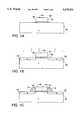
- FIGS. 1A-1Fshow cross-sectional views of successive process steps for formation of a non-symmetrical LDD IGFET in accordance with a first embodiment of the invention.
- FIGS. 2A-2Gshow cross-sectional views of successive process steps for formation of a non-symmetrical LDD IGFET in accordance with a second embodiment of the invention.
- FIGS. 1A-1Fshow cross-sectional views of successive process steps for formation of a non-symmetrical LDD IGFET in accordance with a first embodiment of the invention.
- a gate electrodesuch as polysilicon 106 is disposed on a gate oxide 104, which in turn is disposed on a semiconductor substrate 102 suitable for integrated circuit manufacture.
- substrate 102includes an 8 micron thick P-type planar epitaxial surface layer with a ⁇ 100> orientation and a resistivity of 12 ohm-cm.
- the epitaxial surface layeris disposed on a P+ base layer (not shown).
- a blanket layer of gate oxide 104(such as SiO 2 ) is formed on the top surface of substrate 102 using tube growth at a temperature of 700° to 1,000° C. in an O 2 ambient.
- Gate oxide 104has a thickness in the range of 30 to 200 angstroms.
- a blanket layer of polysilicon 106is deposited by low pressure chemical vapor deposition (LPCVD) on the top surface of gate oxide 104.
- Polysilicon 106has a thickness in the range of 250 to 4,000 angstroms.
- Polysilicon 106is doped by ion implantation of arsenic at a dose in the range of 1 ⁇ 10 15 to 5 ⁇ 10 15 atoms/cm 2 and an energy in the range of 2 to 50 kiloelectron-volts.
- polysilicon 106can be doped by subsequent source/drain implant. Thereafter, polysilicon 106 and gate oxide 104 are patterned using photolithography and an anisotropic dry etch. For submicron dimensions, patterning a photoresist mask (not shown) by I-line photolithography using a mercury vapor lamp is preferred. After the photoresist mask is patterned and an isotropic etch is applied, polysilicon 106 is etched back to provide a gate electrode and gate oxide 104 is etched back to provide a gate insulator. Preferably, a first etchant is applied that is highly selective of polysilicon, then a second etchant is applied that is highly selective of oxides.
- polysilicon 106After etching occurs, polysilicon 106 includes substantially vertical opposing first and second sidewalls 103 and 105, respectively, defining a length of the gate electrode.
- the gate oxide 104is substantially aligned with the first and second sidewalls 103 and 105.
- a light dose of a first dopantis implanted into the semiconductor substrate to provide a lightly doped source region 108 and a lightly doped drain region 110.
- the structureis subjected to ion implantation of arsenic at a dose in the range of 1 ⁇ 10 13 to 5 ⁇ 10 14 atoms/cm 2 and an energy in the range of 2 to 50 kiloelectron-volts.
- the lightly doped source region 108, substantially aligned with the first sidewall 103, and the lightly doped drain region 110, substantially aligned with the second sidewall 105are formed at and below the surface of substrate 102.
- Lightly doped source and drain regions 108 and 110, respectively,are doped N- with a dopant concentration in the range of about 1 ⁇ 10 17 to 1 ⁇ 10 18 atoms/cm 3 , and a junction depth in the range of 0.01 to 0.15 microns.
- insulating spacersare formed on the first sidewall 103 and the second sidewall 105.
- a layer of oxidesuch as SiO 2
- the oxide filmis etched, by reactive ion etching, to form first and second spacers 112 and 114, respectively, adjacent the first and second sidewalls 103 and 105, respectively.
- the first and second spacers 112 and 114respectively, each extend a lateral distance in the range of 200 to 2000 angstroms, and have essentially the same height as polysilicon 106.
- a masking film 116such as a photoresist film, is formed over the lightly doped drain region 110, the second spacer 114, the second sidewall 105 and a part of the top surface of the polysilicon 106, to define a third sidewall of the gate electrode.
- the masking film 116has an opening which exposes a portion of the top surface of the polysilicon 106, the first spacer 112, and the first sidewall 103.
- the polysilicon 106 exposed through the opening in the masking fill 116is etched to provide a third sidewall 117 in polysilicon 106 opposite the second sidewall 105, thereby eliminating the first sidewall 103 and reducing the length of the gate electrode.
- the first spacer 112may be etched before or after the polysilicon 106 exposed through the opening of the masking fill 116 is etched. For instance, a wet etch may be used to etch the first spacer 112 and then a dry etch may be used to remove the polysilicon 106 exposed through the opening of the masking film 116, or the wet etch may be applied after the dry etch.
- both the first spacer 112 and the polysilicon 106 exposed through the opening of the masking film 116may be etched simultaneously with a dry etch. If the polysilicon 106 exposed through the opening of the masking fill 116 is etched first, then the first spacer 112 and gate oxide 104 outside of the polysilicon 106 may be etched before implanting a second dopant, as shown in FIG. 1E, or etched after implanting the second dopant (not shown).
- the length or channel length of a gate electrodeis in the range of 0.35 to 0.40 microns, however, in the present invention wherein the gate electrode sidewalls are formed in sequence, an advantage is obtained whereby the channel length may be reduced.
- U.S. patent application Ser. No. 08/682,233entitled “Method Of Forming A Gate Electrode For An IGFET", (Gardner et at), filed concurrently herewith and incorporated by reference, which describes a method for forming the edges of a gate electrode in sequence, rather than simultaneously, using optical photolithography technology, which provides extremely narrow gate electrode lengths (or channel lengths).
- the masking film 116is removed and a heavy dose of a second dopant is implanted into the semiconductor substrate 102 to provide a heavily doped drain region 118 adjacent to and outside the second spacer 114 and a heavily doped source region 120 substantially aligned with the third sidewall 117.
- the heavily doped drain region 118 and heavily doped source region 120are formed in substrate 102 using the polysilicon 106 and the second spacer 114 as implant masks.
- the implantis performed using arsenic at a dosage of 1 ⁇ 10 15 to 5 ⁇ 10 15 atoms/cm 2 and an energy in the range of 2 to 50 kiloelectron-volts.
- the heavily doped drain region 118 and heavily doped source region 120are formed at and below the surface of substrate 102 and are doped N+ with a dopant concentration in the range of 1 ⁇ 10 18 to 1 ⁇ 10 19 atoms/cm 3 , and a depth in the range of 0.02 to 0.3 microns.
- the heavily doped drain region 118 and the lightly doped drain region 110together form a drain in the semiconductor substrate 102.
- the entire lightly doped source region 108, an N- region,is converted into an N+ region and effectively eliminated if the first spacer 112 is removed before implanting the second dopant.
- a primary difference between the second embodiment and the first embodimentis that, in the second embodiment, an additional step of implanting a third dopant after forming the spacers and before forming the third sidewall of the gate electrode is performed.
- the elements for the second embodimente.g., substrate 202, gate oxide 204, etc.
- the elements for the first embodimente.g., substrate 102, gate oxide 104, etc.
- the description of related elements and process stepsneed not be repeated.
- FIGS. 2A-2Gshow cross sectional views of successive process steps for formation of a non-symmetrical LDD-IGFET in accordance with a second embodiment of the invention.
- gate oxide 204is disposed on substrate 202
- polysilicon 206is disposed on gate oxide 204.
- Polysilicon 206has substantially vertical opposing first and second sidewalls 203 and 205, respectively, defining a gate electrode.
- a light dose of a first dopantis implanted into the semiconductor substrate to provide a lightly doped source region 208 substantially aligned with the first sidewall 203 and a lightly doped drain region 210 substantially aligned with the second sidewall 205.
- first and second spacers 212 and 214are formed adjacent the first and second sidewalls 203 and 205, respectively.
- a heavy dose of a third dopantis implanted into the semiconductor substrate 202, as shown in FIG. 2D.
- the polysilicon 206 and first and second spacers 212 and 214, respectively,are used as implant masks.
- the implantis performed using arsenic at a dosage of 1 ⁇ 10 15 to 5 ⁇ 10 15 atoms/cm 2 and an energy in the range of 2 to 50 kiloelectron-volts.
- a heavily doped source region 215 and heavily doped drain region 218are formed at and below the surface of substrate 202.
- the heavily doped drain region 218is substantially adjacent to and outside the second spacer 214 and the heavily doped source region 215 is substantially adjacent to and outside the first spacer 212.
- the heavily doped source and drain regions 215 and 218, respectively,are doped N+ and have a dopant concentration in the range of 1 ⁇ 10 18 to 1 ⁇ 10 19 atoms/cm 3 , and a depth in the range of 0.02 to 0.3 microns.
- heavily doped source region 215 and heavily doped drain region 218are implanted with a substantially greater energy, and therefore have a substantially greater depth than lightly doped source region 208 and lightly doped drain region 210.
- a portion of the lightly doped source and drain regions 208 and 210, respectively,are retained beneath the first and second spacers 212 and 214, respectively.
- the heavily doped drain region 218 and the lightly doped drain region 210together form a drain in the semiconductor substrate 202.
- a masking film 216such as a photoresist film, is formed over the heavily doped drain region 218, the lightly doped drain region 210, the second spacer 214, the second sidewall 205, and at least a part of the top surface of the polysilicon 206, to define a third sidewall of the gate electrode.
- the masking film 216has an opening which exposes a portion of the top surface of polysilicon 206, the first spacer 212 and the first sidewall 203.
- the polysilicon 206, exposed through the opening in the masking film 216is etched to provide a third sidewall 217 of polysilicon 206 opposite to the second sidewall 205, thereby eliminating the first sidewall 203 and reducing the length of the gate electrode.
- the first spacer 212may be etched before or after the polysilicon 206 exposed through the opening in the masking film 216 is etched.
- the channel length of a gate electrodeis in the range of 0.35 to 0.40 microns, however, in the present invention wherein the sidewalls are formed in sequence an advantage is obtained whereby the channel length may be reduced.
- the masking film 216remains in place and a heavy dose of a second dopant is implanted into the semiconductor substrate 202 using the masking film 216 as an implant mask.
- the implantis performed using arsenic at a dosage of 1 ⁇ 10 15 to 5 ⁇ 10 15 atoms/cm 2 and an energy in the range of 2 to 50 kiloelectron-volts.
- a heavily doped source region 222is formed at and below the surface of substrate 202 and substantially aligned with the third sidewall 217.
- the heavily doped source region 222has a dopant concentration in the range of 1 ⁇ 10 18 to 1 ⁇ 10 19 atoms/cm 3 , and a depth in the range of 0.02 to 0.3 microns.
- the region of the heavily doped source region 215 substantially adjacent to and outside of the first spacer 212has an increased dopant concentration and therefore a lower resistance after the implant of the second dopant.
- the first spacer 212 and gate oxide 204 outside of the polysilicon 206may be etched before implanting the second dopant, as shown in FIG. 2F, or left in place during the implant of the second dopant (not shown). If the first spacer 212 is removed before the implant of the second dopant, then the entire lightly doped source region 208, a N- region, is converted into an N+ region and effectively eliminated.
- the masking film 216is removed after implanting the second dopant. However, the masking film 216 may be removed before implanting the second dopant (not shown).
- the second spacer 214then acts as an implant mask to protect the lightly doped drain region 210, and the heavily doped drain region 218 will have an increased dopant concentration and therefore a lower resistance after implanting the second dopant.
- the present inventionis also well-suited for forming P-channel MOSFETs as well as N-channel MOSFETs.
- Boronis a commonly used P-type dopant. Boron tends to diffuse much faster than typical N-type dopants such as arsenic and phosphorus. For instance, for the heavily doped regions the structure is subjected to ion implantation of boron at a dose in the range of 1 ⁇ 10 15 to 5 ⁇ 10 15 atoms/cm 2 and an energy in the range of 2 to 50 kiloelectron-volts.
- the structureis subjected to ion implantation of boron at a dose in the range of 1 ⁇ 10 13 to 5 ⁇ 10 14 atoms/era 2 and an energy in the range of 5 to 50 kiloelectron-volts.
- the gate oxide insulating filmmay remain on the surface of the semiconductor substrate (not shown).
- Further processing steps in the fabrication of IGFETstypically include forming a thick oxide layer over the active regions, forming contact windows in the oxide layer to expose the drain, source and gate electrode, forming appropriate interconnect metallization in the contact windows, and forming a passivation layer. These further processing steps are conventional and need not be repeated herein. Likewise the principal processing steps disclosed herein may be combined with other steps readily apparent to those skilled in the art.
- the gate electrodecan be a conductor such as a metal
- the gate insulator and the sidewall spacerscan be various dielectrics such as silicon dioxide, silicon nitrite or silicon oxynitride.
- a polysilicon gate electrodecan be deposited doped or undoped, and if deposited undoped can be doped at various stages of the process.
- N-type or P-type dopantscan be used in any of the embodiments described above, and the dopants can be activated by applying various combinations of heat and pressure. Suitable N-type dopants include arsenic and phosphorus; suitable P-type dopants include boron, including boron B 10 and boron B 11 , and BF species such as BF 2 .
- the inventionis well-suited for use in an integrated circuit chip, as well as an electronic system including a microprocessor, a memory, and a system bus.
Landscapes
- Insulated Gate Type Field-Effect Transistor (AREA)
Abstract
Description
Claims (26)
Priority Applications (2)
| Application Number | Priority Date | Filing Date | Title |
|---|---|---|---|
| US08/682,493US5672531A (en) | 1996-07-17 | 1996-07-17 | Method for fabrication of a non-symmetrical transistor |
| PCT/US1997/005176WO1998002918A1 (en) | 1996-07-17 | 1997-03-28 | Method for fabrication of a non-symmetrical transistor |
Applications Claiming Priority (1)
| Application Number | Priority Date | Filing Date | Title |
|---|---|---|---|
| US08/682,493US5672531A (en) | 1996-07-17 | 1996-07-17 | Method for fabrication of a non-symmetrical transistor |
Publications (1)
| Publication Number | Publication Date |
|---|---|
| US5672531Atrue US5672531A (en) | 1997-09-30 |
Family
ID=24739944
Family Applications (1)
| Application Number | Title | Priority Date | Filing Date |
|---|---|---|---|
| US08/682,493Expired - LifetimeUS5672531A (en) | 1996-07-17 | 1996-07-17 | Method for fabrication of a non-symmetrical transistor |
Country Status (2)
| Country | Link |
|---|---|
| US (1) | US5672531A (en) |
| WO (1) | WO1998002918A1 (en) |
Cited By (25)
| Publication number | Priority date | Publication date | Assignee | Title |
|---|---|---|---|---|
| US5759897A (en)* | 1996-09-03 | 1998-06-02 | Advanced Micro Devices, Inc. | Method of making an asymmetrical transistor with lightly and heavily doped drain regions and ultra-heavily doped source region |
| US5789787A (en)* | 1996-09-03 | 1998-08-04 | Advanced Micro Devices, Inc. | Asymmetrical N-channel and P-channel devices |
| US5831306A (en)* | 1996-09-03 | 1998-11-03 | Advanced Micro Devices, Inc. | Asymmetrical transistor with lightly doped drain region, heavily doped source and drain regions, and ultra-heavily doped source region |
| US5877050A (en)* | 1996-09-03 | 1999-03-02 | Advanced Micro Devices, Inc. | Method of making N-channel and P-channel devices using two tube anneals and two rapid thermal anneals |
| US5904529A (en)* | 1997-08-25 | 1999-05-18 | Advanced Micro Devices, Inc. | Method of making an asymmetrical IGFET and providing a field dielectric between active regions of a semiconductor substrate |
| US5918128A (en)* | 1998-06-08 | 1999-06-29 | Advanced Micro Devices, Inc. | Reduced channel length for a high performance CMOS transistor |
| US5923982A (en)* | 1997-04-21 | 1999-07-13 | Advanced Micro Devices, Inc. | Method of making asymmetrical transistor with lightly and heavily doped drain regions and ultra-heavily doped source region using two source/drain implant steps |
| US5933761A (en)* | 1998-02-09 | 1999-08-03 | Lee; Ellis | Dual damascene structure and its manufacturing method |
| US5989967A (en)* | 1998-04-30 | 1999-11-23 | Advanced Micro Devices, Inc. | Transistor with ultra short length defined partially by sidewall oxidation of a gate conductor overlying the channel length |
| US6004849A (en)* | 1997-08-15 | 1999-12-21 | Advanced Micro Devices, Inc. | Method of making an asymmetrical IGFET with a silicide contact on the drain without a silicide contact on the source |
| US6027978A (en)* | 1997-01-28 | 2000-02-22 | Advanced Micro Devices, Inc. | Method of making an IGFET with a non-uniform lateral doping profile in the channel region |
| US6051471A (en)* | 1996-09-03 | 2000-04-18 | Advanced Micro Devices, Inc. | Method for making asymmetrical N-channel and symmetrical P-channel devices |
| US6096615A (en)* | 1998-04-29 | 2000-08-01 | Advanced Micro Devices, Inc. | Method of forming a semiconductor device having narrow gate electrode |
| US6096588A (en)* | 1997-11-01 | 2000-08-01 | Advanced Micro Devices, Inc. | Method of making transistor with selectively doped channel region for threshold voltage control |
| US6153477A (en)* | 1998-04-14 | 2000-11-28 | Advanced Micro Devices, Inc. | Ultra short transistor channel length formed using a gate dielectric having a relatively high dielectric constant |
| US6218251B1 (en)* | 1998-11-06 | 2001-04-17 | Advanced Micro Devices, Inc. | Asymmetrical IGFET devices with spacers formed by HDP techniques |
| US6232183B1 (en)* | 1998-09-28 | 2001-05-15 | United Microelectronics Crop. | Method for fabricating a flash memory |
| US6406950B1 (en) | 2000-12-07 | 2002-06-18 | Advanced Micro Devices, Inc. | Definition of small damascene metal gates using reverse through approach |
| US6500765B2 (en)* | 2001-03-23 | 2002-12-31 | United Microelectronics Corp. | Method for manufacturing dual-spacer structure |
| US6528372B2 (en)* | 2001-06-27 | 2003-03-04 | Advanced Micro Devices, Inc. | Sidewall spacer definition of gates |
| US6808996B1 (en)* | 1999-08-18 | 2004-10-26 | Advanced Micro Devices, Inc. | Method for protecting gate edges from charge gain/loss in semiconductor device |
| US20060284223A1 (en)* | 2005-06-17 | 2006-12-21 | Dongbu Electronics Co., Ltd. | CMOS image sensor and manufacturing method thereof |
| US20080191276A1 (en)* | 2007-02-08 | 2008-08-14 | Taiwan Semiconductor Manufacturing Co., Ltd. | Semiconductor devices and fabrication methods thereof |
| US20080237739A1 (en)* | 2007-03-26 | 2008-10-02 | Fujitsu Limited | Method of manufacturing a semiconductor device and a semiconductor device |
| US20120299097A1 (en)* | 2005-08-29 | 2012-11-29 | Constantin Bulucea | Semiconductor Architecture Having Field-effect Transistors Especially Suitable for Analog Applications |
Families Citing this family (1)
| Publication number | Priority date | Publication date | Assignee | Title |
|---|---|---|---|---|
| EP2246256B1 (en) | 2009-04-29 | 2012-10-24 | Eurocopter Deutschland GmbH | Tension-torque-transmission element for a fenestron blade and method for producing it |
Citations (10)
| Publication number | Priority date | Publication date | Assignee | Title |
|---|---|---|---|---|
| US4272881A (en)* | 1979-07-20 | 1981-06-16 | Rca Corporation | Method for making a closed gate MOS transistor with self-aligned contacts with dual passivation layer |
| DE3939319A1 (en)* | 1988-11-29 | 1990-05-31 | Mitsubishi Electric Corp | ASYMMETRICAL FIELD EFFECT TRANSISTOR AND METHOD FOR THE PRODUCTION THEREOF |
| US5200358A (en)* | 1991-11-15 | 1993-04-06 | At&T Bell Laboratories | Integrated circuit with planar dielectric layer |
| EP0575099A1 (en)* | 1992-06-18 | 1993-12-22 | AT&T Corp. | Method for making a MOS device |
| US5286664A (en)* | 1991-10-01 | 1994-02-15 | Nec Corporation | Method for fabricating the LDD-MOSFET |
| US5296398A (en)* | 1990-04-19 | 1994-03-22 | Mitsubishi Denki Kabushiki Kaisha | Method of making field effect transistor |
| US5424229A (en)* | 1991-09-12 | 1995-06-13 | Kabushiki Kaisha Toshiba | Method for manufacturing MOSFET having an LDD structure |
| JPH07326736A (en)* | 1994-06-01 | 1995-12-12 | Sony Corp | Manufacture of semiconductor device and manufacture of ccd image sensing element |
| US5525552A (en)* | 1995-06-08 | 1996-06-11 | Taiwan Semiconductor Manufacturing Company | Method for fabricating a MOSFET device with a buried contact |
| US5547885A (en)* | 1990-04-03 | 1996-08-20 | Mitsubishi Denki Kabushiki Kaisha | Method of making asymmetric LDD transistor |
Family Cites Families (3)
| Publication number | Priority date | Publication date | Assignee | Title |
|---|---|---|---|---|
| DE3578270D1 (en)* | 1984-04-30 | 1990-07-19 | Gen Electric | FIELD EFFECT TRANSISTOR ARRANGEMENT AND METHOD FOR THE PRODUCTION THEREOF. |
| EP0186058B1 (en)* | 1984-12-21 | 1989-06-28 | Siemens Aktiengesellschaft | Field effect transistor with a high voltage breakdown capacity, and method for its production |
| KR960014718B1 (en)* | 1993-05-14 | 1996-10-19 | Lg Semicon Co Ltd | Method of manufacturing transistor |
- 1996
- 1996-07-17USUS08/682,493patent/US5672531A/ennot_activeExpired - Lifetime
- 1997
- 1997-03-28WOPCT/US1997/005176patent/WO1998002918A1/enactiveApplication Filing
Patent Citations (10)
| Publication number | Priority date | Publication date | Assignee | Title |
|---|---|---|---|---|
| US4272881A (en)* | 1979-07-20 | 1981-06-16 | Rca Corporation | Method for making a closed gate MOS transistor with self-aligned contacts with dual passivation layer |
| DE3939319A1 (en)* | 1988-11-29 | 1990-05-31 | Mitsubishi Electric Corp | ASYMMETRICAL FIELD EFFECT TRANSISTOR AND METHOD FOR THE PRODUCTION THEREOF |
| US5547885A (en)* | 1990-04-03 | 1996-08-20 | Mitsubishi Denki Kabushiki Kaisha | Method of making asymmetric LDD transistor |
| US5296398A (en)* | 1990-04-19 | 1994-03-22 | Mitsubishi Denki Kabushiki Kaisha | Method of making field effect transistor |
| US5424229A (en)* | 1991-09-12 | 1995-06-13 | Kabushiki Kaisha Toshiba | Method for manufacturing MOSFET having an LDD structure |
| US5286664A (en)* | 1991-10-01 | 1994-02-15 | Nec Corporation | Method for fabricating the LDD-MOSFET |
| US5200358A (en)* | 1991-11-15 | 1993-04-06 | At&T Bell Laboratories | Integrated circuit with planar dielectric layer |
| EP0575099A1 (en)* | 1992-06-18 | 1993-12-22 | AT&T Corp. | Method for making a MOS device |
| JPH07326736A (en)* | 1994-06-01 | 1995-12-12 | Sony Corp | Manufacture of semiconductor device and manufacture of ccd image sensing element |
| US5525552A (en)* | 1995-06-08 | 1996-06-11 | Taiwan Semiconductor Manufacturing Company | Method for fabricating a MOSFET device with a buried contact |
Cited By (31)
| Publication number | Priority date | Publication date | Assignee | Title |
|---|---|---|---|---|
| US6078080A (en)* | 1996-09-03 | 2000-06-20 | Advanced Micro Devices, Inc. | Asymmetrical transistor with lightly and heavily doped drain regions and ultra-heavily doped source region |
| US5789787A (en)* | 1996-09-03 | 1998-08-04 | Advanced Micro Devices, Inc. | Asymmetrical N-channel and P-channel devices |
| US5831306A (en)* | 1996-09-03 | 1998-11-03 | Advanced Micro Devices, Inc. | Asymmetrical transistor with lightly doped drain region, heavily doped source and drain regions, and ultra-heavily doped source region |
| US5877050A (en)* | 1996-09-03 | 1999-03-02 | Advanced Micro Devices, Inc. | Method of making N-channel and P-channel devices using two tube anneals and two rapid thermal anneals |
| US6504218B1 (en) | 1996-09-03 | 2003-01-07 | Advanced Micro Devices, Inc. | Asymmetrical N-channel and P-channel devices |
| US5759897A (en)* | 1996-09-03 | 1998-06-02 | Advanced Micro Devices, Inc. | Method of making an asymmetrical transistor with lightly and heavily doped drain regions and ultra-heavily doped source region |
| US6051471A (en)* | 1996-09-03 | 2000-04-18 | Advanced Micro Devices, Inc. | Method for making asymmetrical N-channel and symmetrical P-channel devices |
| US6027978A (en)* | 1997-01-28 | 2000-02-22 | Advanced Micro Devices, Inc. | Method of making an IGFET with a non-uniform lateral doping profile in the channel region |
| US5923982A (en)* | 1997-04-21 | 1999-07-13 | Advanced Micro Devices, Inc. | Method of making asymmetrical transistor with lightly and heavily doped drain regions and ultra-heavily doped source region using two source/drain implant steps |
| US6004849A (en)* | 1997-08-15 | 1999-12-21 | Advanced Micro Devices, Inc. | Method of making an asymmetrical IGFET with a silicide contact on the drain without a silicide contact on the source |
| US5904529A (en)* | 1997-08-25 | 1999-05-18 | Advanced Micro Devices, Inc. | Method of making an asymmetrical IGFET and providing a field dielectric between active regions of a semiconductor substrate |
| US6096588A (en)* | 1997-11-01 | 2000-08-01 | Advanced Micro Devices, Inc. | Method of making transistor with selectively doped channel region for threshold voltage control |
| US5933761A (en)* | 1998-02-09 | 1999-08-03 | Lee; Ellis | Dual damascene structure and its manufacturing method |
| US6153477A (en)* | 1998-04-14 | 2000-11-28 | Advanced Micro Devices, Inc. | Ultra short transistor channel length formed using a gate dielectric having a relatively high dielectric constant |
| US6096615A (en)* | 1998-04-29 | 2000-08-01 | Advanced Micro Devices, Inc. | Method of forming a semiconductor device having narrow gate electrode |
| US5989967A (en)* | 1998-04-30 | 1999-11-23 | Advanced Micro Devices, Inc. | Transistor with ultra short length defined partially by sidewall oxidation of a gate conductor overlying the channel length |
| US5918128A (en)* | 1998-06-08 | 1999-06-29 | Advanced Micro Devices, Inc. | Reduced channel length for a high performance CMOS transistor |
| US6232183B1 (en)* | 1998-09-28 | 2001-05-15 | United Microelectronics Crop. | Method for fabricating a flash memory |
| US6218251B1 (en)* | 1998-11-06 | 2001-04-17 | Advanced Micro Devices, Inc. | Asymmetrical IGFET devices with spacers formed by HDP techniques |
| US6808996B1 (en)* | 1999-08-18 | 2004-10-26 | Advanced Micro Devices, Inc. | Method for protecting gate edges from charge gain/loss in semiconductor device |
| US6406950B1 (en) | 2000-12-07 | 2002-06-18 | Advanced Micro Devices, Inc. | Definition of small damascene metal gates using reverse through approach |
| US6500765B2 (en)* | 2001-03-23 | 2002-12-31 | United Microelectronics Corp. | Method for manufacturing dual-spacer structure |
| US6528372B2 (en)* | 2001-06-27 | 2003-03-04 | Advanced Micro Devices, Inc. | Sidewall spacer definition of gates |
| US20060284223A1 (en)* | 2005-06-17 | 2006-12-21 | Dongbu Electronics Co., Ltd. | CMOS image sensor and manufacturing method thereof |
| US20120299097A1 (en)* | 2005-08-29 | 2012-11-29 | Constantin Bulucea | Semiconductor Architecture Having Field-effect Transistors Especially Suitable for Analog Applications |
| US8395212B2 (en)* | 2005-08-29 | 2013-03-12 | National Semiconductor Corporation | Semiconductor architecture having field-effect transistors especially suitable for analog applications |
| US20080191276A1 (en)* | 2007-02-08 | 2008-08-14 | Taiwan Semiconductor Manufacturing Co., Ltd. | Semiconductor devices and fabrication methods thereof |
| US20080237739A1 (en)* | 2007-03-26 | 2008-10-02 | Fujitsu Limited | Method of manufacturing a semiconductor device and a semiconductor device |
| US7666745B2 (en)* | 2007-03-26 | 2010-02-23 | Fujitsu Microelectronics Limited | Method of manufacturing a semiconductor device and a semiconductor device |
| US20100109082A1 (en)* | 2007-03-26 | 2010-05-06 | Fujitsu Microelectronics Limited | Method of manufacturing a semiconductor device and a semiconductor device |
| US8138550B2 (en) | 2007-03-26 | 2012-03-20 | Fujitsu Semiconductor Limited | Method of manufacturing a semiconductor device and a semiconductor device |
Also Published As
| Publication number | Publication date |
|---|---|
| WO1998002918A1 (en) | 1998-01-22 |
Similar Documents
| Publication | Publication Date | Title |
|---|---|---|
| US5672531A (en) | Method for fabrication of a non-symmetrical transistor | |
| US5930642A (en) | Transistor with buried insulative layer beneath the channel region | |
| US5648286A (en) | Method of making asymmetrical transistor with lightly doped drain region, heavily doped source and drain regions, and ultra-heavily doped source region | |
| US5789300A (en) | Method of making IGFETs in densely and sparsely populated areas of a substrate | |
| US5759897A (en) | Method of making an asymmetrical transistor with lightly and heavily doped drain regions and ultra-heavily doped source region | |
| US6060345A (en) | Method of making NMOS and PMOS devices with reduced masking steps | |
| US6201278B1 (en) | Trench transistor with insulative spacers | |
| US6504218B1 (en) | Asymmetrical N-channel and P-channel devices | |
| US6005272A (en) | Trench transistor with source contact in trench | |
| US5656518A (en) | Method for fabrication of a non-symmetrical transistor | |
| US5888880A (en) | Trench transistor with localized source/drain regions implanted through selectively grown oxide layer | |
| KR100221120B1 (en) | Manufacturing Method of Semiconductor Device | |
| US5654215A (en) | Method for fabrication of a non-symmetrical transistor | |
| US6197645B1 (en) | Method of making an IGFET with elevated source/drain regions in close proximity to gate with sloped sidewalls | |
| US5923982A (en) | Method of making asymmetrical transistor with lightly and heavily doped drain regions and ultra-heavily doped source region using two source/drain implant steps | |
| US5885887A (en) | Method of making an igfet with selectively doped multilevel polysilicon gate | |
| US5904529A (en) | Method of making an asymmetrical IGFET and providing a field dielectric between active regions of a semiconductor substrate | |
| US6258675B1 (en) | High K gate electrode | |
| US6004849A (en) | Method of making an asymmetrical IGFET with a silicide contact on the drain without a silicide contact on the source | |
| US5923980A (en) | Trench transistor with localized source/drain regions implanted through voids in trench | |
| US6077736A (en) | Method of fabricating a semiconductor device | |
| US5827761A (en) | Method of making NMOS and devices with sequentially formed gates having different gate lengths | |
| US5874340A (en) | Method for fabrication of a non-symmetrical transistor with sequentially formed gate electrode sidewalls | |
| US5956591A (en) | Method of making NMOS and PMOS devices having LDD structures using separate drive-in steps | |
| US6008100A (en) | Metal-oxide semiconductor field effect transistor device fabrication process |
Legal Events
| Date | Code | Title | Description |
|---|---|---|---|
| AS | Assignment | Owner name:ADVANCED MICRO DEVICES, INC., CALIFORNIA Free format text:ASSIGNMENT OF ASSIGNORS INTEREST;ASSIGNORS:GARDNER, MARK I.;DUANE, MICHAEL P.;WRISTERS, DERICK J.;REEL/FRAME:008125/0307 Effective date:19960717 | |
| STCF | Information on status: patent grant | Free format text:PATENTED CASE | |
| FEPP | Fee payment procedure | Free format text:PAYOR NUMBER ASSIGNED (ORIGINAL EVENT CODE: ASPN); ENTITY STATUS OF PATENT OWNER: LARGE ENTITY | |
| FPAY | Fee payment | Year of fee payment:4 | |
| FPAY | Fee payment | Year of fee payment:8 | |
| FPAY | Fee payment | Year of fee payment:12 | |
| AS | Assignment | Owner name:GLOBALFOUNDRIES INC., CAYMAN ISLANDS Free format text:AFFIRMATION OF PATENT ASSIGNMENT;ASSIGNOR:ADVANCED MICRO DEVICES, INC.;REEL/FRAME:023119/0083 Effective date:20090630 | |
| AS | Assignment | Owner name:GLOBALFOUNDRIES U.S. INC., NEW YORK Free format text:RELEASE BY SECURED PARTY;ASSIGNOR:WILMINGTON TRUST, NATIONAL ASSOCIATION;REEL/FRAME:056987/0001 Effective date:20201117 |