US5671397A - Sea-of-cells array of transistors - Google Patents
Sea-of-cells array of transistorsDownload PDFInfo
- Publication number
- US5671397A US5671397AUS08/455,503US45550395AUS5671397AUS 5671397 AUS5671397 AUS 5671397AUS 45550395 AUS45550395 AUS 45550395AUS 5671397 AUS5671397 AUS 5671397A
- Authority
- US
- United States
- Prior art keywords
- traces
- metal
- macro
- transistors
- interconnect
- Prior art date
- Legal status (The legal status is an assumption and is not a legal conclusion. Google has not performed a legal analysis and makes no representation as to the accuracy of the status listed.)
- Expired - Fee Related
Links
Images


Classifications
- H—ELECTRICITY
- H10—SEMICONDUCTOR DEVICES; ELECTRIC SOLID-STATE DEVICES NOT OTHERWISE PROVIDED FOR
- H10D—INORGANIC ELECTRIC SEMICONDUCTOR DEVICES
- H10D89/00—Aspects of integrated devices not covered by groups H10D84/00 - H10D88/00
- H10D89/10—Integrated device layouts
- H—ELECTRICITY
- H10—SEMICONDUCTOR DEVICES; ELECTRIC SOLID-STATE DEVICES NOT OTHERWISE PROVIDED FOR
- H10D—INORGANIC ELECTRIC SEMICONDUCTOR DEVICES
- H10D84/00—Integrated devices formed in or on semiconductor substrates that comprise only semiconducting layers, e.g. on Si wafers or on GaAs-on-Si wafers
- H10D84/90—Masterslice integrated circuits
- H10D84/903—Masterslice integrated circuits comprising field effect technology
- H10D84/907—CMOS gate arrays
- H—ELECTRICITY
- H01—ELECTRIC ELEMENTS
- H01L—SEMICONDUCTOR DEVICES NOT COVERED BY CLASS H10
- H01L2924/00—Indexing scheme for arrangements or methods for connecting or disconnecting semiconductor or solid-state bodies as covered by H01L24/00
- H01L2924/0001—Technical content checked by a classifier
- H01L2924/0002—Not covered by any one of groups H01L24/00, H01L24/00 and H01L2224/00
- Y—GENERAL TAGGING OF NEW TECHNOLOGICAL DEVELOPMENTS; GENERAL TAGGING OF CROSS-SECTIONAL TECHNOLOGIES SPANNING OVER SEVERAL SECTIONS OF THE IPC; TECHNICAL SUBJECTS COVERED BY FORMER USPC CROSS-REFERENCE ART COLLECTIONS [XRACs] AND DIGESTS
- Y10—TECHNICAL SUBJECTS COVERED BY FORMER USPC
- Y10S—TECHNICAL SUBJECTS COVERED BY FORMER USPC CROSS-REFERENCE ART COLLECTIONS [XRACs] AND DIGESTS
- Y10S257/00—Active solid-state devices, e.g. transistors, solid-state diodes
- Y10S257/909—Macrocell arrays, e.g. gate arrays with variable size or configuration of cells
Definitions
- the inventionconcerns an Integrated Circuit (IC) architecture in which individual transistors, each of which resides in a "cell,” are arranged in a matrix-like array, thereby forming a "sea" of the cells.
- ICIntegrated Circuit
- Groups of the cellsare interconnected among themselves, by local interconnect, into functional units. (Some of these units are called "MACROs.")
- the local interconnect in the unitsis prohibited from occupying certain layers, such as second-layer metal. The prohibited layer is used instead to connect the individual units to each other.
- Metal Level 2is Used for Local Interconnect
- FIG. 1illustrates a common approach to constructing a CMOS inverter.
- a p-well and an n-wellare constructed in a silicon substrate 3.
- a gate Gcommonly made of polysilicon, extends across the wells.
- an electric field produced by the gate Ggenerates an n-type channel (not shown) in which electrons flow from a source S to a drain D.
- this electric fieldgenerates an opposite type of channel, namely, a p-type channel (not shown), in which holes flow from a source S to a drain D.
- This electric fieldmodulates the flow of the electrons and holes, and thus modulates the current flowing through the inverter.
- bus lines Vss and VddElectric power for the inverter is provided by bus lines Vss and Vdd. These bus lines are generally fabricated in first-layer metal, or METAL 1 in FIG. 2. ("POLY" in that Figure refers to polysilicon.)
- Trace Tis Generally Located in METAL 2
- the two drains D in FIG. 1are connected by an interconnect trace T.
- the Inventor hereinhas observed that this trace T is fabricated using second-layer metal, which is labeled METAL 2 in FIG. 2. Locating this trace T in METAL 2 presents obstacles to routing other traces, as FIG. 3 illustrates. For example, trace TT cannot take the path shown, because trace T blocks the way. Thus, the freedom of routing of traces such as TT is limited by the local interconnect traces T.
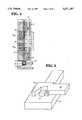
- FIG. 1has been simplified for ease of illustration. Insulating layers are not shown, and the vias V have been simplified.
- FIG. 4illustrates a more detailed view. Vias are not pure vertical columns, as in the simplified FIG. 1, but, for various technical reasons, take the form shown in FIG. 5.
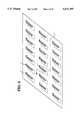
- the cells of a standard cell arraytypically contain a simple logic function, such as an inverter, a NAND gate, or a D-flip flop.
- the transistors in these cellsare specifically designed for the drive requirements of the particular cell, and spacing of these transistors depends upon such factors as the location of contacts within the cells.
- the spacing, or pitch, between rows of cellsis determined by (a) the number of interconnect lines fabricated from METAL 1 (shown in FIG. 2) and (b) the cell height.
- the cell heightin turn, depends upon the transistor configuration within the cells. FIG. 6 illustrates these terms.
- the interconnect lines fabricated from METAL 1are typically laid out by an automated device, or computer program, called a "router,” or “auto-router.” Different routers have different algorithms for laying out the lines, so that different routers will produce different interconnect patterns, even though the end result of the connections may be the same.
- the row pitchis determined by (a) the router used to interconnect the cells in the standard cell array and (b) the height of the individual cells.
- the wiringis very important to efficiently arrange the wiring in an IC because, in general, the wiring running from transistor-to-transistor consumes more space than the transistors themselves. (The wiring consists of traces fabricated from the METAL layers shown in FIG. 2.) Restated, the size of the IC is generally determined by how efficiently the wiring can be routed and compacted, and not by how many transistors the IC contains.
- METALshown in FIG. 2, which is located between rows of cells in FIG. 6, such as at location L1. If additional METAL 2 is required, the cells are then spaced apart, as shown in FIG. 6, so that metal lines can be run between them, as indicated.
- MACROsare frequently incorporated into ICs containing standard cell arrays.
- a MACROis a block of transistors which have been optimized to perform a specific function.
- the layout of the individual transistors, their operating characteristics, and their interconnectionsmay have all been matched to each other for optimum performance.
- a MACROis constructed from different sizes of transistors, which are embedded into the standard cell array as shown in FIG. 7.
- the power busses Vdd and Vsswill be interrupted. To accommodate this interruption, the power busses are re-designed as a ring which surrounds the MACRO.
- FIG. 7shows such a ring generically.
- METAL 2for local interconnect presents obstacles to the free routing of other interconnects over the cell, as illustrated in FIG. 3.
- the ROW PITCHis determined by the cell height and the number of lines of METAL 1 interconnect placed between the cell rows by the auto-router.
- the row pitch in a MACROis generally different from that of a standard cell array into which the MACRO is embedded. This different row pitch disrupts the power bus system, requiring a ring of power busses to be formed around the MACRO. This approach wastes space within the IC.
- a MACROwhen embedded within a standard cell array, uses the same row pitch as that of the standard cell array itself.
- the interconnect within the standard cellis confined to METAL 1 and polysilicon layers, so that METAL 2 is free for routing over the cell.
- the diffusion layer of the transistors within the standard cellsis designed for optimum performance after the layout has been completed, rather than at another time.
- FIG. 1illustrates a CMOS inverter of the prior art.
- FIG. 2illustrates the different layers of metallization used in IC fabrication.
- FIG. 3illustrates the proliferation of traces T, shown in FIG. 1, which can occur when trace T is fabricated in a layer of metallization, such as METAL 2 in FIG. 2.
- FIG. 4illustrates the CMOS inverter of FIG. 1, but in greater detail.
- FIG. 5is a highly simplified depiction of a via of FIG. 4. Like-numbered structures correspond in both Figures.
- the metal in the via Cis a portion of element D1.
- the outline C in FIG. 5is the cutout in the dielectric layer. Metal layer D1 flows down into the via C.
- FIG. 6illustrates a standard cell array
- FIG. 7illustrates a common approach to embedding a MACRO in a standard cell array.
- FIG. 8illustrates one form of the invention.
- FIG. 9illustrates an imaginary grid on which traces are laid out in the prior art.
- FIG. 10A, 10B, 10C, and 10Dillustrate the different effective widths of different traces.
- FIG. 11illustrates different possible ways to pack different traces, of different effective widths, between the traces T of FIGS. 1 and 3.
- FIG. 12illustrates how different traces of different effective widths can be packed on a layer of metallization which lacks the traces T of FIG. 3.
- FIG. 13illustrates embedding of a MACRO into a standard cell array, according to the invention.
- FIG. 14illustrates the WIDTH of the CHANNEL of a field-effect transistor.
- FIG. 15illustrates an analog switch of the prior art.
- FIG. 8shows an inverter, which performs the inversion function, as does the inverter of FIG. 1.
- the connection C between the drains Dis fabricated from the same polysilicon layer as the gate G. Trace C and the gate G are coplanar.
- the polysilicon layeris labeled POLY in FIG. 2.
- the metal traces on a given layerare generally parallel, as shown in FIG. 9. Traces on different layers are connected by vias, indicated by the dashed lines. It can be shown, based on simple assumptions, that, after clearing of METAL 2 of traces T in FIG. 3, the number of metal traces which can be fabricated on METAL 2 is thereby increased by about thirty percent. One contributor to this thirty percent value is the fact that the space formerly occupied by traces T is now available for use, whereas previously it was not.
- trace T1which contains no associated pads for via connections, has an effective width equal to its own width W1.
- W1is assumed to be 1.0 micron, as indicated. (However, in reality, W1 is typically 0.5-2.0 microns.)
- trace T2does contain via-pads P. Its effective width is larger, and equal to the via-pad width W2.
- W2is assumed to be 2.0 microns, as indicated. (However, in reality, W2 is typically 1.0-4.0 microns.)
- a minimum separation D in FIG. 10Bmust exist between adjacent traces.
- the minimum separation Dis based on effective widths, determined by an edge such as E1, and not by edge E2.
- a distance D of 1.0 micronswill be assumed. (In reality, a spacing D of 0.5-2.0 microns, for traces of 0.5-2.0 microns width, is common.)
- This spacing Dcan be allocated to each trace, by attributing one-half to each side of a trace, as shown in FIG. 10C.
- the one-half spacingis labeled D/2. Consequently, trace T1, effectively becomes a rectangle which is 2.0 microns wide, as indicated in FIG. 10C; similarly, trace T2 effectively becomes a rectangle 3.0 microns wide.
- FIG. 11illustrates the eleven possible ways to pack traces T2 (of width W2 in FIG. 11) and T1 (of width W1) between traces T.
- Distance D1is assumed to be 9.0 microns.
- the hatched areasrepresent unused space.
- the average wasted spaceis the numerical average of the hatched areas.
- a statistical analysis of a given IC layoutcan be undertaken to ascertain the actual probabilities of each combination, and may produce a different answer than a simple numerical average of the possibilities in FIG. 11. Nevertheless, it is reasonable to assume that the combinations which leave no wasted space, namely, W2--W2--W2 and W2-W1--W1--W1, will never occur with 100 percent frequency; some wasted space will always occur.
- FIG. 12illustrates how the traces can be packed onto METAL 2 layer shown in FIG. 2, when the traces T in FIG. 3 have been eliminated.
- the traces T1 and T2can be packed with maximum density.
- the only space which is left overis the hatched area at the right. It is clear, based on simple observation, that the wasted space in FIG. 12 is less than that in FIG. 11.
- the eleven possibilities shown in FIG. 11may not all be available. For example, some routing techniques, both computer-executed and manual, follow a rule which requires that all traces lie upon imaginary lines of fixed, uniform spacing, such as the lines H and V in FIG. 9. Under such a role, several possibilities in FIG. 11 would not be available. For example, any possibility which mixes W1 with W2 would be unavailable, (because spacing is not equal with this mixing).
- a MACROis embedded within a standard cell array using the same ROW PITCH in the MACRO as in the array, as indicated in FIG. 13.
- the different sizesindicate that the MACRO's cells need not be the same size as the standard cell array's, although they can be.
- the same power busses, Vdd and Vssfeed both the MACRO cells and the standard cell array cells.
- no local interconnectis made on metal level 2 (labeled METAL 2 in FIG. 2). That is, within the MACRO, there are no traces such as T shown in FIG. 3 located on metal level 2. Stated again, metal level 2 within the MACRO is preferably free of local interconnect.
- the transistors usedcontain channels, through which carriers flow from source to drain.
- One channelis shown in FIG. 14. It is possible to fabricate channels having different WIDTHs, by adjusting the masking used in fabrication. Different WIDTHs result in different associated capacitances, such as the gate capacitance, and also result in different transconductances.
- the channel in a transistor used as a loadpreferably has a narrow WIDTH, to minimize capacitance.
- the channel in a transistor used as a driver (of a load)preferably has a wider WIDTH, to maximize transconductance.
- a given integrated circuitis laid out, using the above principles, including (a) the clearing of METAL 2 of local interconnect, and (b) the use of the same ROW PITCH in a MACRO and a standard cell array in which the MACRO is embedded. Then, the capacitances of selected transistors are computed. (The capacitances cannot be calculated before this time, because the capacitance of each transistor depends on the traces leading to the transistor, as well as on the traces running next to, and over, it.)
- the WIDTHs of the channels of the non-optimal transistorscan be changed.
- the WIDTHs of load transistorscan be reduced, and the WIDTHs of driver transistors can be widened.
- METAL 2is freed of local interconnect, partly by constructing drain-drain interconnect within the polysilicon layer (POLY in FIG. 2).
- Typical Prior-Art interconnect tracesare positioned on an x-y grid of fixed spacing. That is, as shown in FIG. 9, all horizontal traces must run along horizontal dashed lines H, and all vertical traces must run along vertical dashed lines V. (As a consequence, since all vias must lie upon an intersection point of a horizontal trace and a vertical trace, the vias will lie on a grid point GP.)
- the spacing of the tracescan be non-uniform.
- FIG. 12illustrates the non-uniform spacing.
- FIG. 15illustrates an analog switch. (The discussion above has presumed standard cell arrays of CMOS devices; FIG. 15 shows BJTs. The appearance of BJTs is purely incidental.) All of the interconnections in that Figure are "local interconnects,” with two exceptions:
- the line carrying the CONTROL VOLTAGEis not a local interconnect, because it carries the actuation signal for the analog switch. In general, this actuation signal will originate at a location which is unrelated to, and independent of, the location of the analog switch.
- FIG. 15illustrates one definition of "local interconnect.”
- Local interconnectincludes traces which carry signals from one component to another within a given functional block, and which assist in the execution of the block's function.
- the line CONTROL VOLTAGE, which carries the incoming signal,is not local interconnect, because it initiates execution of block's function.
- Integrated circuitare frequently constructed using MACROs and other functional blocks contained in a library.
- Each MACRO and functional blockcan operate isolated, by itself (provided it receives power and input signals).
- the traces contained within each isolated MACRO and functional blockare local interconnect.
- the inventionapplies to integrated circuits having high levels of integration.
- the inventionapplies to ICs of overall dimension of 5 ⁇ 5 mm, or greater.
- Such ICsare fabricated using VLSI/ULSI techniques.
- the power busses Vdd and Vssrun parallel, and they are aligned to both the cells of the standard cell array and the cells of the MACRO.
- a MACRO having a fixed, predetermined layoutis embedded in a standard cell array. Since the placement does not alter the design of the MACRO, the MACRO's timing is not be affected by this embedding.
- the final gate width adjustments(or channel width adjustments), discussed above, are accomplished by the use of computer simulations.
- a series of timing simulations of the circuitare run, in which transistor gate widths are incrementally changed, and the resulting change in the logic timing are observed. If timing is improved, the new increment is likely to be retained. If the timing worsens, the new increment is likely to be rejected.
- a third and fourth layer of metal interconnectcan be utilized in addition to the interconnect, discussed above, provided by (a) the polysilicon layer, (b) METAL 1 and (c) METAL 2 layers. These additional layers maximize the cell density in the layout by providing layers of metal interconnect that can be freely routed over the cells. That is, these layers are not subject to the restrictions discussed above.
Landscapes
- Design And Manufacture Of Integrated Circuits (AREA)
Abstract
Description
Claims (1)
Priority Applications (9)
| Application Number | Priority Date | Filing Date | Title |
|---|---|---|---|
| US08/455,503US5671397A (en) | 1993-12-27 | 1995-05-31 | Sea-of-cells array of transistors |
| US08/837,589US6269466B1 (en) | 1993-12-27 | 1997-04-21 | Method of constructing an integrated circuit utilizing multiple layers of interconnect |
| US09/703,948US6675361B1 (en) | 1993-12-27 | 2000-10-31 | Method of constructing an integrated circuit comprising an embedded macro |
| US09/703,767US6489641B1 (en) | 1993-12-27 | 2000-11-01 | Sea-of-cells array of transistors |
| US09/704,115US6605499B1 (en) | 1993-12-27 | 2000-11-01 | Method of forming sea-of-cells array of transistors |
| US10/125,925US6977399B2 (en) | 1993-12-27 | 2002-04-19 | Sea-of-cells array of transistors |
| US10/463,160US7257779B2 (en) | 1993-12-27 | 2003-06-16 | Sea-of-cells array of transistors |
| US10/601,351US6967361B2 (en) | 1993-12-27 | 2003-06-23 | Sea-of-cells array of transistors |
| US10/719,357US7207025B2 (en) | 1993-12-27 | 2003-11-21 | Sea-of-cells array of transistors |
Applications Claiming Priority (2)
| Application Number | Priority Date | Filing Date | Title |
|---|---|---|---|
| US17465493A | 1993-12-27 | 1993-12-27 | |
| US08/455,503US5671397A (en) | 1993-12-27 | 1995-05-31 | Sea-of-cells array of transistors |
Related Parent Applications (2)
| Application Number | Title | Priority Date | Filing Date |
|---|---|---|---|
| US17465493ADivision | 1993-12-27 | 1993-12-27 | |
| US08/837,589ContinuationUS6269466B1 (en) | 1993-12-27 | 1997-04-21 | Method of constructing an integrated circuit utilizing multiple layers of interconnect |
Related Child Applications (2)
| Application Number | Title | Priority Date | Filing Date |
|---|---|---|---|
| US17465493ADivision | 1993-12-27 | 1993-12-27 | |
| US08/837,589DivisionUS6269466B1 (en) | 1993-12-27 | 1997-04-21 | Method of constructing an integrated circuit utilizing multiple layers of interconnect |
Publications (1)
| Publication Number | Publication Date |
|---|---|
| US5671397Atrue US5671397A (en) | 1997-09-23 |
Family
ID=22636989
Family Applications (6)
| Application Number | Title | Priority Date | Filing Date |
|---|---|---|---|
| US08/455,503Expired - Fee RelatedUS5671397A (en) | 1993-12-27 | 1995-05-31 | Sea-of-cells array of transistors |
| US08/543,335Expired - Fee RelatedUS5869900A (en) | 1993-12-27 | 1995-10-16 | Sea-of-cells array of transistors |
| US08/837,589Expired - LifetimeUS6269466B1 (en) | 1993-12-27 | 1997-04-21 | Method of constructing an integrated circuit utilizing multiple layers of interconnect |
| US09/703,767Expired - LifetimeUS6489641B1 (en) | 1993-12-27 | 2000-11-01 | Sea-of-cells array of transistors |
| US09/704,115Expired - LifetimeUS6605499B1 (en) | 1993-12-27 | 2000-11-01 | Method of forming sea-of-cells array of transistors |
| US10/601,351Expired - LifetimeUS6967361B2 (en) | 1993-12-27 | 2003-06-23 | Sea-of-cells array of transistors |
Family Applications After (5)
| Application Number | Title | Priority Date | Filing Date |
|---|---|---|---|
| US08/543,335Expired - Fee RelatedUS5869900A (en) | 1993-12-27 | 1995-10-16 | Sea-of-cells array of transistors |
| US08/837,589Expired - LifetimeUS6269466B1 (en) | 1993-12-27 | 1997-04-21 | Method of constructing an integrated circuit utilizing multiple layers of interconnect |
| US09/703,767Expired - LifetimeUS6489641B1 (en) | 1993-12-27 | 2000-11-01 | Sea-of-cells array of transistors |
| US09/704,115Expired - LifetimeUS6605499B1 (en) | 1993-12-27 | 2000-11-01 | Method of forming sea-of-cells array of transistors |
| US10/601,351Expired - LifetimeUS6967361B2 (en) | 1993-12-27 | 2003-06-23 | Sea-of-cells array of transistors |
Country Status (1)
| Country | Link |
|---|---|
| US (6) | US5671397A (en) |
Cited By (10)
| Publication number | Priority date | Publication date | Assignee | Title |
|---|---|---|---|---|
| US6489641B1 (en)* | 1993-12-27 | 2002-12-03 | Hyundai Electronics America | Sea-of-cells array of transistors |
| US20020184600A1 (en)* | 2001-04-23 | 2002-12-05 | Howard Sachs | Circuit group design methodologies |
| US6525350B1 (en) | 1999-07-16 | 2003-02-25 | Kawasaki Steel Corporation | Semiconductor integrated circuit basic cell semiconductor integrated circuit using the same |
| US6594813B1 (en)* | 1998-09-23 | 2003-07-15 | Artisan Components, Inc. | Cell architecture with local interconnect and method for making same |
| US6660544B1 (en)* | 2002-11-05 | 2003-12-09 | Oki Electric Industry Co., Ltd. | Method of forming conductive patterns formed in semiconductor integrated circuit device using multilayer interconnection |
| US6675361B1 (en)* | 1993-12-27 | 2004-01-06 | Hyundai Electronics America | Method of constructing an integrated circuit comprising an embedded macro |
| US6711726B2 (en)* | 2000-10-18 | 2004-03-23 | Renesas Technology Corp. | Automatic cell placement and routing apparatus and automatic cell placement and routing method used for the apparatus |
| US20050289493A1 (en)* | 2004-06-15 | 2005-12-29 | Fujitsu Limited | Method and apparatus for designing a layout, and computer product |
| US8051400B2 (en)* | 2008-10-21 | 2011-11-01 | Arm Limited | Modifying integrated circuit layout |
| CN103812501A (en)* | 2014-02-13 | 2014-05-21 | 清华大学 | Phase inverter |
Families Citing this family (12)
| Publication number | Priority date | Publication date | Assignee | Title |
|---|---|---|---|---|
| JP3276003B2 (en)* | 1997-12-15 | 2002-04-22 | 日本電気株式会社 | Semiconductor integrated circuit device and layout method thereof |
| US6388332B1 (en)* | 1999-08-10 | 2002-05-14 | Philips Electronics North America Corporation | Integrated circuit power and ground routing |
| US6385761B1 (en)* | 1999-10-01 | 2002-05-07 | Lsi Logic Corporation | Flexible width cell layout architecture |
| US6532580B1 (en)* | 2000-02-18 | 2003-03-11 | Hewlett-Packard Company | In-place method for inserting repeater buffers in an integrated circuit |
| US6467074B1 (en) | 2000-03-21 | 2002-10-15 | Ammocore Technology, Inc. | Integrated circuit architecture with standard blocks |
| JP3390408B2 (en)* | 2000-05-29 | 2003-03-24 | エヌイーシーマイクロシステム株式会社 | Semiconductor integrated circuit |
| US6492205B1 (en) | 2000-12-26 | 2002-12-10 | Taiwan Semiconductor Manufacturing Company | Utilization of macro power routing area for buffer insertion |
| US6492736B1 (en)* | 2001-03-14 | 2002-12-10 | Lsi Logic Corporation | Power mesh bridge |
| TW200403994A (en)* | 2002-04-04 | 2004-03-16 | Bristol Myers Squibb Co | Oral administration of EPOTHILONES |
| US20040003363A1 (en)* | 2002-06-27 | 2004-01-01 | Nickolai Odilavadze | Integrated circuit design and manufacture utilizing layers having a predetermined layout |
| TWI252067B (en)* | 2005-02-14 | 2006-03-21 | Benq Corp | Labeling method and software utilizing the same, and PCB and electronic device utilizing the same |
| US9870166B2 (en)* | 2014-09-15 | 2018-01-16 | Apple Inc. | Securely sharing cached data |
Citations (40)
| Publication number | Priority date | Publication date | Assignee | Title |
|---|---|---|---|---|
| US4143178A (en)* | 1976-07-07 | 1979-03-06 | Tokyo Shibaura Electric Co., Ltd. | Manufacturing method of semiconductor devices |
| US4151635A (en)* | 1971-06-16 | 1979-05-01 | Signetics Corporation | Method for making a complementary silicon gate MOS structure |
| US4229756A (en)* | 1979-02-09 | 1980-10-21 | Tektronix, Inc. | Ultra high speed complementary MOS device |
| US4244001A (en)* | 1979-09-28 | 1981-01-06 | Rca Corporation | Fabrication of an integrated injection logic device with narrow basewidth |
| US4317690A (en)* | 1980-06-18 | 1982-03-02 | Signetics Corporation | Self-aligned double polysilicon MOS fabrication |
| US4525809A (en)* | 1981-01-26 | 1985-06-25 | Nippon Electric Co., Ltd. | Integrated circuit |
| US4584653A (en)* | 1983-03-22 | 1986-04-22 | Fujitsu Limited | Method for manufacturing a gate array integrated circuit device |
| US4593205A (en)* | 1983-07-01 | 1986-06-03 | Motorola, Inc. | Macrocell array having an on-chip clock generator |
| US4638458A (en)* | 1984-03-30 | 1987-01-20 | Kabushiki Kaisha Toshiba | Semiconductor memory address lines with varied interval contact holes |
| US4682202A (en)* | 1983-07-29 | 1987-07-21 | Fujitsu Limited | Master slice IC device |
| US4686758A (en)* | 1984-06-27 | 1987-08-18 | Honeywell Inc. | Three-dimensional CMOS using selective epitaxial growth |
| US4701642A (en)* | 1986-04-28 | 1987-10-20 | International Business Machines Corporation | BICMOS binary logic circuits |
| US4845544A (en)* | 1986-03-26 | 1989-07-04 | Hitachi, Ltd. | Semiconductor integrated device having a field-effect transistor type memory cell array and peripheral circuitry structure |
| US4849344A (en)* | 1986-12-11 | 1989-07-18 | Fairchild Semiconductor Corporation | Enhanced density modified isoplanar process |
| US4905073A (en)* | 1987-06-22 | 1990-02-27 | At&T Bell Laboratories | Integrated circuit with improved tub tie |
| US4989062A (en)* | 1987-06-19 | 1991-01-29 | Fujitsu Limited | Semiconductor integrated circuit device having multilayer power supply lines |
| US4999518A (en)* | 1989-12-08 | 1991-03-12 | International Business Machines Corp. | MOS switching circuit having gate enhanced lateral bipolar transistor |
| US5003199A (en)* | 1990-02-26 | 1991-03-26 | International Business Machines Corp. | Emitter coupled logic circuit having an active pull-down output stage |
| US5008208A (en)* | 1988-12-07 | 1991-04-16 | Honeywell Inc. | Method of making planarized, self-aligned bipolar integrated circuits |
| US5013679A (en)* | 1988-09-09 | 1991-05-07 | Kabushiki Kaisha Toshiba | Cell capacitor of a dynamic random access memory and a method of manufacturing the same |
| US5032530A (en)* | 1989-10-27 | 1991-07-16 | Micron Technology, Inc. | Split-polysilicon CMOS process incorporating unmasked punchthrough and source/drain implants |
| US5037766A (en)* | 1988-12-06 | 1991-08-06 | Industrial Technology Research Institute | Method of fabricating a thin film polysilicon thin film transistor or resistor |
| US5045726A (en)* | 1990-05-16 | 1991-09-03 | North American Philips Corporation | Low power programming circuit for user programmable digital logic array |
| US5049515A (en)* | 1990-03-09 | 1991-09-17 | Intel Corporation, Inc. | Method of making a three-dimensional memory cell with integral select transistor |
| US5081518A (en)* | 1989-05-24 | 1992-01-14 | National Semiconductor Corporation | Use of a polysilicon layer for local interconnect in a CMOS or BICMOS technology incorporating sidewall spacers |
| US5124776A (en)* | 1989-03-14 | 1992-06-23 | Fujitsu Limited | Bipolar integrated circuit having a unit block structure |
| US5126279A (en)* | 1988-12-19 | 1992-06-30 | Micron Technology, Inc. | Single polysilicon cross-coupled resistor, six-transistor SRAM cell design technique |
| US5162884A (en)* | 1991-03-27 | 1992-11-10 | Sgs-Thomson Microelectronics, Inc. | Insulated gate field-effect transistor with gate-drain overlap and method of making the same |
| US5168072A (en)* | 1990-10-12 | 1992-12-01 | Texas Instruments Incorporated | Method of fabricating an high-performance insulated-gate field-effect transistor |
| US5175118A (en)* | 1988-09-20 | 1992-12-29 | Mitsubishi Denki Kabushiki Kaisha | Multiple layer electrode structure for semiconductor device and method of manufacturing thereof |
| US5225991A (en)* | 1991-04-11 | 1993-07-06 | International Business Machines Corporation | Optimized automated macro embedding for standard cell blocks |
| US5294822A (en)* | 1989-07-10 | 1994-03-15 | Texas Instruments Incorporated | Polycide local interconnect method and structure |
| US5296755A (en)* | 1990-11-29 | 1994-03-22 | Hitachi, Ltd. | High speed BI CMOS logic circuit and a semiconductor integrated circuit device using same |
| US5298805A (en)* | 1991-08-29 | 1994-03-29 | National Semiconductor Corporation | Versatile and efficient cell-to-local bus interface in a configurable logic array |
| US5313079A (en)* | 1992-06-22 | 1994-05-17 | Vlsi Technology, Inc. | Gate array bases with flexible routing |
| US5313101A (en)* | 1990-08-28 | 1994-05-17 | Mitsubishi Denki Kabushiki Kaisha | Interconnection structure of semiconductor integrated circuit device |
| US5314832A (en)* | 1989-09-28 | 1994-05-24 | Commissariat A L'energie Atomique | Process for the production of a high voltage MIS integrated circuit |
| US5341049A (en)* | 1991-07-22 | 1994-08-23 | Hitachi, Ltd. | Integrated circuit having alternate rows of logic cells and I/O cells |
| US5388055A (en)* | 1990-09-07 | 1995-02-07 | Fujitsu Limited | Semiconductor integrated circuit having polycell structure and method of designing the same |
| US5444285A (en)* | 1992-01-31 | 1995-08-22 | Analog Devices, Inc. | Complementary bipolar polysilicon emitter devices |
Family Cites Families (27)
| Publication number | Priority date | Publication date | Assignee | Title |
|---|---|---|---|---|
| US1143178A (en)* | 1914-03-09 | 1915-06-15 | Joseph E Evans | Drilling-machine. |
| US2294822A (en)* | 1939-03-01 | 1942-09-01 | Albree George Norman | Cartridge |
| US3461361A (en) | 1966-02-24 | 1969-08-12 | Rca Corp | Complementary mos transistor integrated circuits with inversion layer formed by ionic discharge bombardment |
| US3481361A (en)* | 1966-11-04 | 1969-12-02 | Motorola Inc | Latch assembly for differential valve |
| US3808475A (en)* | 1972-07-10 | 1974-04-30 | Amdahl Corp | Lsi chip construction and method |
| US4589008A (en)* | 1980-01-28 | 1986-05-13 | Rca Corporation | Apparatus for electrically joining the ends of substantially parallel semiconductor lines |
| US4383474A (en)* | 1980-05-09 | 1983-05-17 | The United States Of America As Represented By The Secretary Of The Army | Muzzle position sensor |
| US4482810A (en)* | 1982-09-30 | 1984-11-13 | Storage Technology Partners | Electron beam exposure system |
| US4742383A (en)* | 1983-01-12 | 1988-05-03 | International Business Machines Corporation | Multi-function FET masterslice cell |
| CH661301A5 (en)* | 1983-10-07 | 1987-07-15 | Textilma Ag | Warp knitting machine. |
| US4630219A (en) | 1983-11-23 | 1986-12-16 | International Business Machines Corporation | Element placement method |
| JPS61100947A (en)* | 1984-10-22 | 1986-05-19 | Toshiba Corp | Semiconductor integrated circuit device |
| DE68910445T2 (en)* | 1988-09-01 | 1994-02-24 | Fujitsu Ltd | Integrated semiconductor circuit. |
| US5410173A (en)* | 1991-01-28 | 1995-04-25 | Kikushima; Ken'ichi | Semiconductor integrated circuit device |
| JP3027990B2 (en)* | 1991-03-18 | 2000-04-04 | 富士通株式会社 | Method for manufacturing semiconductor device |
| US5166902A (en)* | 1991-03-18 | 1992-11-24 | United Technologies Corporation | SRAM memory cell |
| US5182884A (en)* | 1991-04-12 | 1993-02-02 | Tarics Alexander G | Integrated building system and method |
| EP0554059B1 (en)* | 1992-01-31 | 2002-07-24 | Kabushiki Kaisha Toshiba | Electromagnetic flowmeter |
| JPH05315448A (en)* | 1992-04-27 | 1993-11-26 | Nec Corp | Integrated circuit device and its layout method |
| US5286518A (en)* | 1992-04-30 | 1994-02-15 | Vlsi Technology, Inc. | Integrated-circuit processing with progressive intermetal-dielectric deposition |
| US5342794A (en)* | 1992-09-10 | 1994-08-30 | Vlsi Technology, Inc. | Method for forming laterally graded deposit-type emitter for bipolar transistor |
| US5432707A (en)* | 1993-02-12 | 1995-07-11 | International Business Machines Corporation | Automated circuit design |
| US5654898A (en)* | 1993-05-10 | 1997-08-05 | Cascade Design Automation Corporation | Timing-driven integrated circuit layout through device sizing |
| US5452245A (en)* | 1993-09-07 | 1995-09-19 | Motorola, Inc. | Memory efficient gate array cell |
| US5671397A (en)* | 1993-12-27 | 1997-09-23 | At&T Global Information Solutions Company | Sea-of-cells array of transistors |
| US6675361B1 (en)* | 1993-12-27 | 2004-01-06 | Hyundai Electronics America | Method of constructing an integrated circuit comprising an embedded macro |
| IL111708A (en)* | 1994-11-21 | 1998-03-10 | Chip Express Israel Ltd | Mapping of gate arrays |
- 1995
- 1995-05-31USUS08/455,503patent/US5671397A/ennot_activeExpired - Fee Related
- 1995-10-16USUS08/543,335patent/US5869900A/ennot_activeExpired - Fee Related
- 1997
- 1997-04-21USUS08/837,589patent/US6269466B1/ennot_activeExpired - Lifetime
- 2000
- 2000-11-01USUS09/703,767patent/US6489641B1/ennot_activeExpired - Lifetime
- 2000-11-01USUS09/704,115patent/US6605499B1/ennot_activeExpired - Lifetime
- 2003
- 2003-06-23USUS10/601,351patent/US6967361B2/ennot_activeExpired - Lifetime
Patent Citations (41)
| Publication number | Priority date | Publication date | Assignee | Title |
|---|---|---|---|---|
| US4151635A (en)* | 1971-06-16 | 1979-05-01 | Signetics Corporation | Method for making a complementary silicon gate MOS structure |
| US4143178A (en)* | 1976-07-07 | 1979-03-06 | Tokyo Shibaura Electric Co., Ltd. | Manufacturing method of semiconductor devices |
| US4229756A (en)* | 1979-02-09 | 1980-10-21 | Tektronix, Inc. | Ultra high speed complementary MOS device |
| US4244001A (en)* | 1979-09-28 | 1981-01-06 | Rca Corporation | Fabrication of an integrated injection logic device with narrow basewidth |
| US4317690A (en)* | 1980-06-18 | 1982-03-02 | Signetics Corporation | Self-aligned double polysilicon MOS fabrication |
| US4525809A (en)* | 1981-01-26 | 1985-06-25 | Nippon Electric Co., Ltd. | Integrated circuit |
| US4584653A (en)* | 1983-03-22 | 1986-04-22 | Fujitsu Limited | Method for manufacturing a gate array integrated circuit device |
| US4593205A (en)* | 1983-07-01 | 1986-06-03 | Motorola, Inc. | Macrocell array having an on-chip clock generator |
| US4682202A (en)* | 1983-07-29 | 1987-07-21 | Fujitsu Limited | Master slice IC device |
| US4638458A (en)* | 1984-03-30 | 1987-01-20 | Kabushiki Kaisha Toshiba | Semiconductor memory address lines with varied interval contact holes |
| US4686758A (en)* | 1984-06-27 | 1987-08-18 | Honeywell Inc. | Three-dimensional CMOS using selective epitaxial growth |
| US4845544A (en)* | 1986-03-26 | 1989-07-04 | Hitachi, Ltd. | Semiconductor integrated device having a field-effect transistor type memory cell array and peripheral circuitry structure |
| US4701642A (en)* | 1986-04-28 | 1987-10-20 | International Business Machines Corporation | BICMOS binary logic circuits |
| US4849344A (en)* | 1986-12-11 | 1989-07-18 | Fairchild Semiconductor Corporation | Enhanced density modified isoplanar process |
| US4989062A (en)* | 1987-06-19 | 1991-01-29 | Fujitsu Limited | Semiconductor integrated circuit device having multilayer power supply lines |
| US4905073A (en)* | 1987-06-22 | 1990-02-27 | At&T Bell Laboratories | Integrated circuit with improved tub tie |
| US5013679A (en)* | 1988-09-09 | 1991-05-07 | Kabushiki Kaisha Toshiba | Cell capacitor of a dynamic random access memory and a method of manufacturing the same |
| US5175118A (en)* | 1988-09-20 | 1992-12-29 | Mitsubishi Denki Kabushiki Kaisha | Multiple layer electrode structure for semiconductor device and method of manufacturing thereof |
| US5037766A (en)* | 1988-12-06 | 1991-08-06 | Industrial Technology Research Institute | Method of fabricating a thin film polysilicon thin film transistor or resistor |
| US5008208A (en)* | 1988-12-07 | 1991-04-16 | Honeywell Inc. | Method of making planarized, self-aligned bipolar integrated circuits |
| US5126279A (en)* | 1988-12-19 | 1992-06-30 | Micron Technology, Inc. | Single polysilicon cross-coupled resistor, six-transistor SRAM cell design technique |
| US5124776A (en)* | 1989-03-14 | 1992-06-23 | Fujitsu Limited | Bipolar integrated circuit having a unit block structure |
| US5081518A (en)* | 1989-05-24 | 1992-01-14 | National Semiconductor Corporation | Use of a polysilicon layer for local interconnect in a CMOS or BICMOS technology incorporating sidewall spacers |
| US5294822A (en)* | 1989-07-10 | 1994-03-15 | Texas Instruments Incorporated | Polycide local interconnect method and structure |
| US5314832A (en)* | 1989-09-28 | 1994-05-24 | Commissariat A L'energie Atomique | Process for the production of a high voltage MIS integrated circuit |
| US5032530A (en)* | 1989-10-27 | 1991-07-16 | Micron Technology, Inc. | Split-polysilicon CMOS process incorporating unmasked punchthrough and source/drain implants |
| US4999518A (en)* | 1989-12-08 | 1991-03-12 | International Business Machines Corp. | MOS switching circuit having gate enhanced lateral bipolar transistor |
| US5003199A (en)* | 1990-02-26 | 1991-03-26 | International Business Machines Corp. | Emitter coupled logic circuit having an active pull-down output stage |
| US5049515A (en)* | 1990-03-09 | 1991-09-17 | Intel Corporation, Inc. | Method of making a three-dimensional memory cell with integral select transistor |
| US5045726A (en)* | 1990-05-16 | 1991-09-03 | North American Philips Corporation | Low power programming circuit for user programmable digital logic array |
| US5313101A (en)* | 1990-08-28 | 1994-05-17 | Mitsubishi Denki Kabushiki Kaisha | Interconnection structure of semiconductor integrated circuit device |
| US5388055A (en)* | 1990-09-07 | 1995-02-07 | Fujitsu Limited | Semiconductor integrated circuit having polycell structure and method of designing the same |
| US5168072A (en)* | 1990-10-12 | 1992-12-01 | Texas Instruments Incorporated | Method of fabricating an high-performance insulated-gate field-effect transistor |
| US5296755A (en)* | 1990-11-29 | 1994-03-22 | Hitachi, Ltd. | High speed BI CMOS logic circuit and a semiconductor integrated circuit device using same |
| US5162884A (en)* | 1991-03-27 | 1992-11-10 | Sgs-Thomson Microelectronics, Inc. | Insulated gate field-effect transistor with gate-drain overlap and method of making the same |
| US5225991A (en)* | 1991-04-11 | 1993-07-06 | International Business Machines Corporation | Optimized automated macro embedding for standard cell blocks |
| US5341049A (en)* | 1991-07-22 | 1994-08-23 | Hitachi, Ltd. | Integrated circuit having alternate rows of logic cells and I/O cells |
| US5298805A (en)* | 1991-08-29 | 1994-03-29 | National Semiconductor Corporation | Versatile and efficient cell-to-local bus interface in a configurable logic array |
| US5444285A (en)* | 1992-01-31 | 1995-08-22 | Analog Devices, Inc. | Complementary bipolar polysilicon emitter devices |
| US5541120A (en)* | 1992-01-31 | 1996-07-30 | Analog Devices, Inc. | Method of making complementary bipolar polysilicon emitter devices |
| US5313079A (en)* | 1992-06-22 | 1994-05-17 | Vlsi Technology, Inc. | Gate array bases with flexible routing |
Non-Patent Citations (15)
| Title |
|---|
| "10K-Gate GaAs JFET Sea of Gates", by H. Kawasaki et al., IEEE Journal of Solid-State Circuits, vol. 26, No. 10, Oct. 1991, pp. 1367-1370. |
| "A Comprehensive CAD System for High-Performance 300K-Circuit ASIC Logic Chips", by J. Panner et al., IEEE Journal of Solid-State Circuits, vol. 26, No. 3, Mar. 1991, pp. 300-309. |
| "A Design- System for ASIC's with Macrocells", by B. Korte et al., IEEE, Euro ASIC '90, 1990, . 220-224. |
| "An Efficient Algorithm for Some Multirow Layout Problems", by J. Feldman et al., IEEE Transactions on Computer-Aided Design of Integrated Circuits and Systems, vol. 12, No. 8, Aug. 1993, pp. 1178-1185. |
| "Application of AIGaAs/GaAs HBT's to High-Speed CML Logic Family Fabrication", by M. Madihian et al., IEEE Transactions on Electron Devices, vol. 36, No. 4, Apr. 1989, p. 625-631. |
| "Combining Partioning and Global Routing in a Sea-of-Cells Design", by B. Korte et al., IEEE Comuter-Aided Design, 1989 International Conference, pp. 98-101. |
| "GaAs MESFET and Si CMOS Cointegration and Circuit Techniques", by H. Shichijo et al., IEEE, GaAs IC Symposium, Sep. 1988, pp. 239-242. |
| 10K Gate GaAs JFET Sea of Gates , by H. Kawasaki et al., IEEE Journal of Solid State Circuits, vol. 26, No. 10, Oct. 1991, pp. 1367 1370.* |
| A Comprehensive CAD System for High Performance 300K Circuit ASIC Logic Chips , by J. Panner et al., IEEE Journal of Solid State Circuits, vol. 26, No. 3, Mar. 1991, pp. 300 309.* |
| A Design System for ASIC s with Macrocells , by B. Korte et al., IEEE, Euro ASIC 90, 1990, . 220 224.* |
| An Efficient Algorithm for Some Multirow Layout Problems , by J. Feldman et al., IEEE Transactions on Computer Aided Design of Integrated Circuits and Systems, vol. 12, No. 8, Aug. 1993, pp. 1178 1185.* |
| Application of AIGaAs/GaAs HBT s to High Speed CML Logic Family Fabrication , by M. Madihian et al., IEEE Transactions on Electron Devices, vol. 36, No. 4, Apr. 1989, p. 625 631.* |
| Combining Partioning and Global Routing in a Sea of Cells Design , by B. Korte et al., IEEE Comuter Aided Design, 1989 International Conference, pp. 98 101.* |
| GaAs MESFET and Si CMOS Cointegration and Circuit Techniques , by H. Shichijo et al., IEEE, GaAs IC Symposium, Sep. 1988, pp. 239 242.* |
| IBM Technical Disclosure Bulletin; vol. 25, No. 4; Sep. 1982; Structured Macro; E.H. Stoops.* |
Cited By (24)
| Publication number | Priority date | Publication date | Assignee | Title |
|---|---|---|---|---|
| US20040078769A1 (en)* | 1993-12-27 | 2004-04-22 | Crafts Harold S. | Sea-of-cells array of transistors |
| US7257779B2 (en) | 1993-12-27 | 2007-08-14 | Magnachip Semiconductor, Ltd. | Sea-of-cells array of transistors |
| US6489641B1 (en)* | 1993-12-27 | 2002-12-03 | Hyundai Electronics America | Sea-of-cells array of transistors |
| US6967361B2 (en) | 1993-12-27 | 2005-11-22 | Magnachip Semiconductor, Ltd. | Sea-of-cells array of transistors |
| US6605499B1 (en) | 1993-12-27 | 2003-08-12 | Hyundai Electronics America, Inc. | Method of forming sea-of-cells array of transistors |
| US7207025B2 (en) | 1993-12-27 | 2007-04-17 | Magnachip Semiconductor, Ltd. | Sea-of-cells array of transistors |
| US6675361B1 (en)* | 1993-12-27 | 2004-01-06 | Hyundai Electronics America | Method of constructing an integrated circuit comprising an embedded macro |
| US20040005738A1 (en)* | 1993-12-27 | 2004-01-08 | Hyundai Electronics America | Sea-of-cells array of transistors |
| US20040039998A1 (en)* | 1993-12-27 | 2004-02-26 | Crafts Harold S. | Sea-of-cells array of transistors |
| US6977399B2 (en) | 1993-12-27 | 2005-12-20 | Hynix Semiconductor Inc. | Sea-of-cells array of transistors |
| US6594813B1 (en)* | 1998-09-23 | 2003-07-15 | Artisan Components, Inc. | Cell architecture with local interconnect and method for making same |
| US6525350B1 (en) | 1999-07-16 | 2003-02-25 | Kawasaki Steel Corporation | Semiconductor integrated circuit basic cell semiconductor integrated circuit using the same |
| US6711726B2 (en)* | 2000-10-18 | 2004-03-23 | Renesas Technology Corp. | Automatic cell placement and routing apparatus and automatic cell placement and routing method used for the apparatus |
| US20050028128A1 (en)* | 2001-04-23 | 2005-02-03 | Telairity Semiconductor, Inc. | Circuit group design methodologies |
| US6910199B2 (en)* | 2001-04-23 | 2005-06-21 | Telairity Semiconductor, Inc. | Circuit group design methodologies |
| US20050022146A1 (en)* | 2001-04-23 | 2005-01-27 | Telairity Semiconductor, Inc. | Circuit group design methodologies |
| US7234123B2 (en) | 2001-04-23 | 2007-06-19 | Telairity Semiconductor, Inc. | Circuit group design methodologies |
| US20020184600A1 (en)* | 2001-04-23 | 2002-12-05 | Howard Sachs | Circuit group design methodologies |
| US6660544B1 (en)* | 2002-11-05 | 2003-12-09 | Oki Electric Industry Co., Ltd. | Method of forming conductive patterns formed in semiconductor integrated circuit device using multilayer interconnection |
| US20050289493A1 (en)* | 2004-06-15 | 2005-12-29 | Fujitsu Limited | Method and apparatus for designing a layout, and computer product |
| US7302665B2 (en)* | 2004-06-15 | 2007-11-27 | Fujitsu Limited | Method and apparatus for designing a layout, and computer product |
| US8051400B2 (en)* | 2008-10-21 | 2011-11-01 | Arm Limited | Modifying integrated circuit layout |
| CN103812501A (en)* | 2014-02-13 | 2014-05-21 | 清华大学 | Phase inverter |
| CN103812501B (en)* | 2014-02-13 | 2017-02-15 | 清华大学 | Phase inverter |
Also Published As
| Publication number | Publication date |
|---|---|
| US6489641B1 (en) | 2002-12-03 |
| US5869900A (en) | 1999-02-09 |
| US20040005738A1 (en) | 2004-01-08 |
| US6269466B1 (en) | 2001-07-31 |
| US6967361B2 (en) | 2005-11-22 |
| US6605499B1 (en) | 2003-08-12 |
Similar Documents
| Publication | Publication Date | Title |
|---|---|---|
| US5671397A (en) | Sea-of-cells array of transistors | |
| US7257779B2 (en) | Sea-of-cells array of transistors | |
| US5493135A (en) | Symmetrical multi-layer metal logic array with continuous substrate taps and extension portions for increased gate density | |
| US4851892A (en) | Standard cell array having fake gate for isolating devices from supply voltages | |
| US6765245B2 (en) | Gate array core cell for VLSI ASIC devices | |
| US6987293B2 (en) | Semiconductor integrated circuit device and standard cell placement design method | |
| JP3154411B2 (en) | Two metal layer integrated circuit gate array laid out by CAD | |
| US5051917A (en) | Method of combining gate array and standard cell circuits on a common semiconductor chip | |
| US20150048425A1 (en) | Gate array architecture with multiple programmable regions | |
| JPH10335612A (en) | High density gate array cell structure and manufacturing method thereof | |
| EP0788166A2 (en) | Integrated circuit chip having gate array book personalisation using local interconnect | |
| US4786613A (en) | Method of combining gate array and standard cell circuits on a common semiconductor chip | |
| US8788984B2 (en) | Gate array architecture with multiple programmable regions | |
| US5369595A (en) | Method of combining gate array and standard cell circuits on a common semiconductor chip | |
| US4999698A (en) | Interconnection arrangement for a gate array | |
| US5635737A (en) | Symmetrical multi-layer metal logic array with extension portions for increased gate density and a testability area | |
| JPH09293844A (en) | High density gate array cell structure and manufacturing method thereof | |
| JPH04216668A (en) | Semiconductor integrated circuit | |
| KR100269494B1 (en) | Small semiconductor device using soi cmos technology | |
| WO1993026044A1 (en) | Symmetrical multi-layer metal logic array with continuous substrate taps | |
| JP2000223575A (en) | Semiconductor device design method, semiconductor device, and semiconductor device manufacturing method | |
| US5701021A (en) | Cell architecture for mixed signal applications | |
| EP1143520B1 (en) | High density and high speed cell array architecture | |
| JPH10150175A (en) | Semiconductor integrated circuit and method of manufacturing the same | |
| JPH04106973A (en) | Semiconductor integrated circuit device |
Legal Events
| Date | Code | Title | Description |
|---|---|---|---|
| AS | Assignment | Owner name:SYMBIOS, INC ., COLORADO Free format text:CHANGE OF NAME;ASSIGNOR:SYMBIOS LOGIC INC.;REEL/FRAME:009089/0936 Effective date:19971210 | |
| AS | Assignment | Owner name:LEHMAN COMMERCIAL PAPER INC., AS ADMINISTRATIVE AG Free format text:SECURITY AGREEMENT;ASSIGNORS:HYUNDAI ELECTRONICS AMERICA, A CORP. OF CALIFORNIA;SYMBIOS, INC., A CORP. OF DELAWARE;REEL/FRAME:009396/0441 Effective date:19980226 | |
| AS | Assignment | Owner name:HYUNDAI ELECTRONICS AMERICA, CALIFORNIA Free format text:TERMINATION AND LICENSE AGREEMENT;ASSIGNOR:SYMBIOS, INC.;REEL/FRAME:009596/0539 Effective date:19980806 | |
| FEPP | Fee payment procedure | Free format text:PAYOR NUMBER ASSIGNED (ORIGINAL EVENT CODE: ASPN); ENTITY STATUS OF PATENT OWNER: LARGE ENTITY | |
| FPAY | Fee payment | Year of fee payment:4 | |
| SULP | Surcharge for late payment | ||
| AS | Assignment | Owner name:HYNIX SEMICONDUCTOR AMERICA INC., CALIFORNIA Free format text:CHANGE OF NAME;ASSIGNOR:HYUNDAI ELECTRONICS AMERICA;REEL/FRAME:015246/0599 Effective date:20010412 Owner name:HYNIX SEMICONDUCTOR INC., KOREA, REPUBLIC OF Free format text:ASSIGNMENT OF ASSIGNORS INTEREST;ASSIGNOR:HYNIX SEMICONDUCTOR AMERICA, INC.;REEL/FRAME:015279/0556 Effective date:20040920 | |
| AS | Assignment | Owner name:MAGNACHIP SEMICONDUCTOR, LTD., KOREA, REPUBLIC OF Free format text:ASSIGNMENT OF ASSIGNORS INTEREST;ASSIGNOR:HYNIX SEMICONDUCTOR, INC.;REEL/FRAME:016216/0649 Effective date:20041004 | |
| FPAY | Fee payment | Year of fee payment:8 | |
| AS | Assignment | Owner name:U.S. BANK NATIONAL ASSOCIATION, AS COLLATERAL TRUS Free format text:SECURITY INTEREST;ASSIGNOR:MAGNACHIP SEMICONDUCTOR, LTD.;REEL/FRAME:016470/0530 Effective date:20041223 | |
| AS | Assignment | Owner name:SYMBIOS, INC., COLORADO Free format text:RELEASE OF SECURITY INTEREST;ASSIGNOR:LEHMAN COMMERICAL PAPER INC.;REEL/FRAME:016602/0895 Effective date:20050107 Owner name:HYUNDAI ELECTRONICS AMERICA, CALIFORNIA Free format text:RELEASE OF SECURITY INTEREST;ASSIGNOR:LEHMAN COMMERICAL PAPER INC.;REEL/FRAME:016602/0895 Effective date:20050107 | |
| AS | Assignment | Owner name:TAIWAN SEMICONDUCTOR MANUFACTURING CO., LTD., TAIW Free format text:ASSIGNMENT OF ASSIGNORS INTEREST;ASSIGNORS:NCR CORPORATION;MAGNACHIP SEMICONDUCTOR, LTD.;REEL/FRAME:021398/0702;SIGNING DATES FROM 20071114 TO 20071115 | |
| REMI | Maintenance fee reminder mailed | ||
| LAPS | Lapse for failure to pay maintenance fees | ||
| STCH | Information on status: patent discontinuation | Free format text:PATENT EXPIRED DUE TO NONPAYMENT OF MAINTENANCE FEES UNDER 37 CFR 1.362 | |
| FP | Lapsed due to failure to pay maintenance fee | Effective date:20090923 |