US5670018A - Isotropic silicon etch process that is highly selective to tungsten - Google Patents
Isotropic silicon etch process that is highly selective to tungstenDownload PDFInfo
- Publication number
- US5670018A US5670018AUS08/430,011US43001195AUS5670018AUS 5670018 AUS5670018 AUS 5670018AUS 43001195 AUS43001195 AUS 43001195AUS 5670018 AUS5670018 AUS 5670018A
- Authority
- US
- United States
- Prior art keywords
- silicon
- etch process
- oxide
- mask oxide
- tungsten
- Prior art date
- Legal status (The legal status is an assumption and is not a legal conclusion. Google has not performed a legal analysis and makes no representation as to the accuracy of the status listed.)
- Expired - Fee Related
Links
- XUIMIQQOPSSXEZ-UHFFFAOYSA-NSiliconChemical compound[Si]XUIMIQQOPSSXEZ-UHFFFAOYSA-N0.000titleclaimsabstractdescription62
- 229910052710siliconInorganic materials0.000titleclaimsabstractdescription62
- 239000010703siliconSubstances0.000titleclaimsabstractdescription62
- 238000000034methodMethods0.000titleclaimsabstractdescription52
- 230000008569processEffects0.000titleclaimsabstractdescription49
- WFKWXMTUELFFGS-UHFFFAOYSA-NtungstenChemical compound[W]WFKWXMTUELFFGS-UHFFFAOYSA-N0.000titleclaimsabstractdescription39
- 229910052721tungstenInorganic materials0.000titleclaimsabstractdescription39
- 239000010937tungstenSubstances0.000titleclaimsabstractdescription39
- 229910021420polycrystalline siliconInorganic materials0.000claimsabstractdescription53
- 229920005591polysiliconPolymers0.000claimsabstractdescription53
- VYPSYNLAJGMNEJ-UHFFFAOYSA-NSilicium dioxideChemical compoundO=[Si]=OVYPSYNLAJGMNEJ-UHFFFAOYSA-N0.000claimsabstractdescription19
- 238000001816coolingMethods0.000claimsabstractdescription13
- 239000001307heliumSubstances0.000claimsabstractdescription13
- 229910052734heliumInorganic materials0.000claimsabstractdescription13
- SWQJXJOGLNCZEY-UHFFFAOYSA-Nhelium atomChemical compound[He]SWQJXJOGLNCZEY-UHFFFAOYSA-N0.000claimsabstractdescription13
- 229910052814silicon oxideInorganic materials0.000claimsabstractdescription13
- 238000005530etchingMethods0.000claimsabstractdescription7
- 229910052581Si3N4Inorganic materials0.000claimsabstractdescription5
- 229910021421monocrystalline siliconInorganic materials0.000claimsabstractdescription5
- HQVNEWCFYHHQES-UHFFFAOYSA-Nsilicon nitrideChemical compoundN12[Si]34N5[Si]62N3[Si]51N64HQVNEWCFYHHQES-UHFFFAOYSA-N0.000claimsabstractdescription5
- XKRFYHLGVUSROY-UHFFFAOYSA-NArgonChemical compound[Ar]XKRFYHLGVUSROY-UHFFFAOYSA-N0.000claimsdescription8
- XPDWGBQVDMORPB-UHFFFAOYSA-NFluoroformChemical compoundFC(F)FXPDWGBQVDMORPB-UHFFFAOYSA-N0.000claimsdescription7
- BOTDANWDWHJENH-UHFFFAOYSA-NTetraethyl orthosilicateChemical compoundCCO[Si](OCC)(OCC)OCCBOTDANWDWHJENH-UHFFFAOYSA-N0.000claimsdescription7
- 238000001514detection methodMethods0.000claimsdescription5
- 229910052786argonInorganic materials0.000claimsdescription4
- BLRPTPMANUNPDV-UHFFFAOYSA-NSilaneChemical group[SiH4]BLRPTPMANUNPDV-UHFFFAOYSA-N0.000claimsdescription3
- 238000005229chemical vapour depositionMethods0.000claimsdescription3
- 238000005336crackingMethods0.000claimsdescription3
- 238000001704evaporationMethods0.000claimsdescription3
- 238000004544sputter depositionMethods0.000claimsdescription3
- 230000015572biosynthetic processEffects0.000abstractdescription2
- 230000000379polymerizing effectEffects0.000abstractdescription2
- 239000010410layerSubstances0.000description26
- CPELXLSAUQHCOX-UHFFFAOYSA-NHydrogen bromideChemical compoundBrCPELXLSAUQHCOX-UHFFFAOYSA-N0.000description21
- 229910000042hydrogen bromideInorganic materials0.000description10
- 235000012431wafersNutrition0.000description10
- YCKRFDGAMUMZLT-UHFFFAOYSA-NFluorine atomChemical compound[F]YCKRFDGAMUMZLT-UHFFFAOYSA-N0.000description9
- 229910052731fluorineInorganic materials0.000description9
- 239000011737fluorineSubstances0.000description9
- 238000009792diffusion processMethods0.000description7
- 238000004519manufacturing processMethods0.000description6
- 239000004065semiconductorSubstances0.000description6
- KZBUYRJDOAKODT-UHFFFAOYSA-NChlorineChemical compoundClClKZBUYRJDOAKODT-UHFFFAOYSA-N0.000description5
- 239000004020conductorSubstances0.000description4
- 239000012212insulatorSubstances0.000description3
- 235000012239silicon dioxideNutrition0.000description3
- 239000000377silicon dioxideSubstances0.000description3
- 230000007812deficiencyEffects0.000description2
- 238000000151depositionMethods0.000description2
- 230000008021depositionEffects0.000description2
- 150000002500ionsChemical class0.000description2
- 238000002955isolationMethods0.000description2
- 238000005498polishingMethods0.000description2
- 230000009467reductionEffects0.000description2
- -1silicon dioxideChemical compound0.000description2
- 239000000758substrateSubstances0.000description2
- OKTJSMMVPCPJKN-UHFFFAOYSA-NCarbonChemical compound[C]OKTJSMMVPCPJKN-UHFFFAOYSA-N0.000description1
- ZAMOUSCENKQFHK-UHFFFAOYSA-NChlorine atomChemical compound[Cl]ZAMOUSCENKQFHK-UHFFFAOYSA-N0.000description1
- 229910052799carbonInorganic materials0.000description1
- 230000008859changeEffects0.000description1
- 239000000460chlorineSubstances0.000description1
- 229910052801chlorineInorganic materials0.000description1
- 238000004140cleaningMethods0.000description1
- 238000007796conventional methodMethods0.000description1
- 238000005516engineering processMethods0.000description1
- 230000008020evaporationEffects0.000description1
- 239000007789gasSubstances0.000description1
- 230000010354integrationEffects0.000description1
- 230000002045lasting effectEffects0.000description1
- 229910052751metalInorganic materials0.000description1
- 239000002184metalSubstances0.000description1
- 230000004048modificationEffects0.000description1
- 238000012986modificationMethods0.000description1
- 230000003287optical effectEffects0.000description1
- 229920002120photoresistant polymerPolymers0.000description1
- 229920000642polymerPolymers0.000description1
- 229920006254polymer filmPolymers0.000description1
- 239000013047polymeric layerSubstances0.000description1
- 239000002243precursorSubstances0.000description1
- 239000000376reactantSubstances0.000description1
- 239000000126substanceSubstances0.000description1
Images

Classifications
- H—ELECTRICITY
- H01—ELECTRIC ELEMENTS
- H01L—SEMICONDUCTOR DEVICES NOT COVERED BY CLASS H10
- H01L21/00—Processes or apparatus adapted for the manufacture or treatment of semiconductor or solid state devices or of parts thereof
- H01L21/02—Manufacture or treatment of semiconductor devices or of parts thereof
- H01L21/04—Manufacture or treatment of semiconductor devices or of parts thereof the devices having potential barriers, e.g. a PN junction, depletion layer or carrier concentration layer
- H01L21/18—Manufacture or treatment of semiconductor devices or of parts thereof the devices having potential barriers, e.g. a PN junction, depletion layer or carrier concentration layer the devices having semiconductor bodies comprising elements of Group IV of the Periodic Table or AIIIBV compounds with or without impurities, e.g. doping materials
- H01L21/30—Treatment of semiconductor bodies using processes or apparatus not provided for in groups H01L21/20 - H01L21/26
- H01L21/302—Treatment of semiconductor bodies using processes or apparatus not provided for in groups H01L21/20 - H01L21/26 to change their surface-physical characteristics or shape, e.g. etching, polishing, cutting
- H01L21/306—Chemical or electrical treatment, e.g. electrolytic etching
- H—ELECTRICITY
- H01—ELECTRIC ELEMENTS
- H01L—SEMICONDUCTOR DEVICES NOT COVERED BY CLASS H10
- H01L21/00—Processes or apparatus adapted for the manufacture or treatment of semiconductor or solid state devices or of parts thereof
- H01L21/02—Manufacture or treatment of semiconductor devices or of parts thereof
- H01L21/04—Manufacture or treatment of semiconductor devices or of parts thereof the devices having potential barriers, e.g. a PN junction, depletion layer or carrier concentration layer
- H01L21/18—Manufacture or treatment of semiconductor devices or of parts thereof the devices having potential barriers, e.g. a PN junction, depletion layer or carrier concentration layer the devices having semiconductor bodies comprising elements of Group IV of the Periodic Table or AIIIBV compounds with or without impurities, e.g. doping materials
- H01L21/30—Treatment of semiconductor bodies using processes or apparatus not provided for in groups H01L21/20 - H01L21/26
- H01L21/31—Treatment of semiconductor bodies using processes or apparatus not provided for in groups H01L21/20 - H01L21/26 to form insulating layers thereon, e.g. for masking or by using photolithographic techniques; After treatment of these layers; Selection of materials for these layers
- H01L21/3205—Deposition of non-insulating-, e.g. conductive- or resistive-, layers on insulating layers; After-treatment of these layers
- H01L21/321—After treatment
- H01L21/3213—Physical or chemical etching of the layers, e.g. to produce a patterned layer from a pre-deposited extensive layer
- H01L21/32133—Physical or chemical etching of the layers, e.g. to produce a patterned layer from a pre-deposited extensive layer by chemical means only
- H01L21/32135—Physical or chemical etching of the layers, e.g. to produce a patterned layer from a pre-deposited extensive layer by chemical means only by vapour etching only
- H01L21/32136—Physical or chemical etching of the layers, e.g. to produce a patterned layer from a pre-deposited extensive layer by chemical means only by vapour etching only using plasmas
- H01L21/32137—Physical or chemical etching of the layers, e.g. to produce a patterned layer from a pre-deposited extensive layer by chemical means only by vapour etching only using plasmas of silicon-containing layers
- Y—GENERAL TAGGING OF NEW TECHNOLOGICAL DEVELOPMENTS; GENERAL TAGGING OF CROSS-SECTIONAL TECHNOLOGIES SPANNING OVER SEVERAL SECTIONS OF THE IPC; TECHNICAL SUBJECTS COVERED BY FORMER USPC CROSS-REFERENCE ART COLLECTIONS [XRACs] AND DIGESTS
- Y10—TECHNICAL SUBJECTS COVERED BY FORMER USPC
- Y10S—TECHNICAL SUBJECTS COVERED BY FORMER USPC CROSS-REFERENCE ART COLLECTIONS [XRACs] AND DIGESTS
- Y10S438/00—Semiconductor device manufacturing: process
- Y10S438/963—Removing process residues from vertical substrate surfaces
Definitions
- the present inventiongenerally relates to the manufacture of semiconductor devices and, more particularly, to an isotropic etch process for removing a hard-mask oxide and temporary (sacrificial) silicon mandrel used in forming tungsten studs in high density semiconductor devices, such as 64 megabyte Dynamic Random Access Memory (DRAM) chips.
- DRAMDynamic Random Access Memory
- borderless diffusion and borderless gate contact structuresare an effective approach to increase the circuit integration density.
- a fully borderless diffusion contactis permitted to overlap the gate conductor and the device isolation regions in a Dynamic Random Access Memory (DRAM) array.
- the resulting DRAM cell areacan be reduced by approximately 40% compared with a fully-landed diffusion contact, as described, for example, by D. Kenney et al., "A Buried-Plate Trench Cell for a 64-MB DRAM", 1992 Symposium on VLSI Technology, Seattle, Wash.
- a borderless gate-conductor contactis also permitted to overlap the isolation regions.
- the conventional fabrication processrequires a temporary (sacrificial) mandrel structure for the fabrication of contact vias.
- the mandrelmay, for example, be a polysilicon structure which is globally planarized by chemical-mechanical polishing (CMP) to the level of the gate cap dielectric, plus a polysilicon extension layer which serves as an etch stop for the mask oxide.
- CMPchemical-mechanical polishing
- a hard-mask oxide layerOver this layer is formed a hard-mask oxide layer.
- These polysilicon layersare anisotropically etched using the oxide hard mask and a fluorine-free etch chemistry to obtain a high selectivity (>50:1) of the etch rate of polysilicon to the etch rate of the gate-cap dielectric, thereby forming high-aspect vias in the mandrel.
- These high-aspect-ratio viasare then filled with chemical vapor deposited (CVD) tungsten (W), and the tungsten is polished back down to the hard-mask oxide layer to form Contact to Diffusion (CD) and Contact to Gate (CG) studs.
- CVDchemical vapor deposited
- CDContact to Diffusion
- CGContact to Gate
- Cl 2 /HBrChlorine/Hydrogen Bromide
- a reduction in the widening of the CG holesis deskable, as the widening of the holes results in an increase of CD to CG shorts.
- an isotropic silicon etch processcomprising the steps of: (1) providing a wafer with tungsten studs having a mask oxide and silicon in contact with the tungsten studs; (2) providing backside helium cooling to the wafer; (3) plasma stripping the mask oxide with an about 3:1 ratio of CF 4 /CHF 3 and Argon; (4) removing the backside helium cooling; and (5) plasma stripping the silicon with an etchant.
- the inventionprovides for a silicon etch process comprising the steps of: (1) providing a wafer with tungsten studs having a mask oxide and silicon in contact with the tungsten studs; (2) providing backside helium cooling at about 12 Torr to the wafer; (3) plasma stripping the mask oxide with an about 3:1 ratio of CF 4 /CHF 3 and Argon utilizing endpoint detection; (4) overetching the mask oxide for a period of about 28 percent of the endpoint detection time; (5) removing the backside helium cooling; and (6) plasma stripping the silicon with an etchant.
- the above removal processoccurs following the formation of the gate stacks and tungsten studs and is required to etch silicon selectively to both the gate cap dielectric and the tungsten.
- the gate cap dielectricmay be silicon nitride or silicon dioxide.
- the siliconmay be undoped polysilicon, doped polysilicon, or single crystal silicon.
- the disclosed isotropic processuses hydrogen bromide (HBr) as a single species reactant to selectively etch the silicon with respect to the tungsten and the gate cap dielectric.
- Residual silicon stringersare removed by increasing the temperature of the substrate by terminating the normal helium (He) cooling of the backside of the wafers during the HBr etch.
- Isotropic etching with NF 3 and SF 6can also be used to eliminate the residual silicon stringers, but tungsten stud height will be lost as a result of the fluorine chemistry.
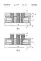
- FIG. 1is a cross-sectional view of the gate stacks and tungsten contact to diffusion (CD) studs prior to mandrel etch;
- FIG. 2is a cross-sectional view of the gate stacks and CD studs as in FIG. 1 after hard-mask oxide removal;
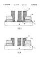
- FIG. 3is a cross-sectional view of the gate stacks and CD studs as in FIG. 2 after mandrel polysilicon etch;
- FIG. 4is a cross-sectional view of the gate stacks and CD studs as in FIG. 3 after NF 3 /SF 6 clean-up etch;
- FIG. 5is a flow chart of the steps of the present invention.
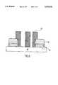
- FIG. 6is a cross-sectional view of the gate stacks and CD studs after the polysilicon is stripped with HBr chemistry and backside He cooling is turned off according to the present invention.
- FIG. 1a cross-sectional view of a semiconductor device designated generally as reference numeral 10, and having gate stacks and Contact to Diffusion (CD) studs surrounded by a hard-mask oxide and temporary silicon mandrel, prior to a silicon etch process.
- CDContact to Diffusion
- layers 13 and 15may be formed of not only undoped polysilicon, but also doped polysilicon or single crystal silicon.
- process parameters of the present inventiondiscussed further below, would remain approximately the same regardless of the type of silicon utilized in layers 13 and 15.
- the semiconductor device 10comprises a substrate 14 on which gate conductors 11 have been formed.
- the gate conductors 11are covered by a gate-cap dielectric 16 of silicon nitride or silicon dioxide, and over this structure is formed a mandrel polysilicon layer 13 which is planarized by chemical-mechanical polishing (CMP) to the level of the gate-cap dielectric.
- CMPchemical-mechanical polishing
- This mandrel polysilicon layeris then extended as a polysilicon layer 15.
- a hard-mask oxide layer 18is formed over the extended layer 15 to define openings to be formed in the polysilicon layers 13 and 15.
- the polysilicon layersare etched using the mask and fluorine-free etch chemistry to obtain high-aspect-ratio vias in the polysilicon mandrel. These vias are filled using CVD tungsten (W) deposition followed by tungsten CMP to form the CD studs 12.
- the hard-mask oxide layer 18 and temporary polysilicon fill, comprising mandrel layer 13 and extended layer 15,are necessary in order to etch the borderless contacts selectively to the gate oxide cap. After fulfilling this purpose, the hard-mask oxide and polysilicon fill have to be replaced by an insulator.
- the purpose of the subsequent mandrel strip processis to remove all of the mask oxide and polysilicon fill around the studs and between the gate stacks while minimizing the attack on the tungsten studs and the gate cap dielectric.
- a reactive ion etch (RIE)is first used to strip the hard-mask oxide layer 18. See FIG. 2. This results in mask oxide removal with minimal attack on the tungsten studs 12.
- a polymeric layer or film 17, mainly composed from carbon and fluorine,is formed during the mask oxide RIE. This polymer film helps to protect the tungsten from being etched, thus maintaining its stud height during the mask oxide RIE. Polymer deposition during the mask oxide RIE is required because the free fluorine would otherwise attack the tungsten.
- Isotropic etchingis required for the mandrel polysilicon strip process because the polymeric caps 17 on top of the studs 12 would otherwise mask the polysilicon if an anisotropic etch were used.
- FIG. 3illustrates a conventional method of stripping the mandrel polysilicon layers 13 and 15 with HBr chemistry.
- some mandrel polysilicon residual stringers 19remain attached to the base of the CD studs 12 and gate insulators 16 following this etch step. These residual stringers 19 cause stud to stud leakage and must therefore be removed.
- FIG. 5represents a flow chart of the process of the present invention, which overcomes the aforementioned problem of removing the residual polysilicon stringers 19, but with minimal reduction of the CD stud height.
- a waferas for example the semiconductor device 10 in FIG. 1, is prepared for etching and is provided in step 20 (see FIG. 5).
- the hard-mask oxide 18is etched using an oxide etch at approximately 240 mTorr pressure, 1200 watts power, and having an electrode gap of 1.015 cm.
- the hard-mask oxidecan be a silicon oxide (SiO x ), such as silicon dioxide, which may be deposited in many ways, for example, by "cracking" of tetraethylorthosilicate (TEOS), sputtering from a SiO x target, or evaporation of SiO x .
- TEOStetraethylorthosilicate
- Other chemical vapor depositions with precursors other than TEOS, such as SiH 4 and N 2 O,may also be used to form the mask oxide.
- the mask oxide etchuses an approximate combination of Ar at 200 sccm (standard cubic centimeters per minute), CF 4 at 60 sccm and CHF 3 at 20 sccm.
- the helium (He) clamp pressureis kept at 12 Torr during this step.
- the oxide etchis stopped using conventional endpoint detection, which measures the intensity of a desired wavelength with an optical spectrometer.
- step 30the wafer may then be overetched to ensure complete hard-mask oxide removal. This step exposes the wafer to the same conditions as in the previous step 20, for a time of about 28% of that of the initial mask oxide etch in step 20.
- the next three steps--steps 40, 50, and 60--demonstrate the polysilicon etch process according to the present inventionare set to zero (0) Torr. By removing this backside cooling, the wafer temperatures for steps 40-60 reach on the order of 260° C. Also, during all three steps, the polysilicon is plasma stripped using HBr chemistry at about 300 sccm while the power remains constant at about 575 watts.
- step 40the extended polysilicon layer 15 is etched.
- the waferis exposed to a pressure of 650 mTorr and the electrode gap is widened from 1.015 cm in the previous step to 1.3 cm.
- the duration of this etch stepis about 20 seconds.
- the pressureis lowered to 350 mTorr and the electrode gap is reduced to 0.8 cm.
- the duration of this etch stepis about 20 seconds. This step is done to "break through” any interface between the mandrel polysilicon layer 13 and the extended polysilicon layer 15.
- FIG. 6is a cross-sectional view of the resulting gate stacks and CD studs after completion of step 60.
- the process of the present inventionis effective in removing the polysilicon stringers even where the above described process parameter target values (e.g., power, pressure, gas flow rate, time, and electrode gap spacing) vary by about +/-20%.
- process parameter target valuese.g., power, pressure, gas flow rate, time, and electrode gap spacing
- the selectivity of etching polysilicon to that of tungstengreatly increases from 6:1 to 15:1. Also, the polysilicon stringers are removed from the sidewalls while maintaining the high selectivity of polysilicon to both the tungsten studs and the gate cap dielectric.
- oxide etch steps (20 and 30) and silicon etch steps (40-60)may be performed in the same chamber or in separate chambers. That is, one can do the oxide etch, change the electrode gap, and then do the silicon etch steps in the same chamber, or use two separate chambers to perform the functions.
Landscapes
- Engineering & Computer Science (AREA)
- Physics & Mathematics (AREA)
- Manufacturing & Machinery (AREA)
- Power Engineering (AREA)
- Microelectronics & Electronic Packaging (AREA)
- Computer Hardware Design (AREA)
- Condensed Matter Physics & Semiconductors (AREA)
- General Physics & Mathematics (AREA)
- General Chemical & Material Sciences (AREA)
- Chemical Kinetics & Catalysis (AREA)
- Chemical & Material Sciences (AREA)
- Plasma & Fusion (AREA)
- Drying Of Semiconductors (AREA)
- Electrodes Of Semiconductors (AREA)
- Crystals, And After-Treatments Of Crystals (AREA)
- Insulated Gate Type Field-Effect Transistor (AREA)
- Silicon Compounds (AREA)
- ing And Chemical Polishing (AREA)
- Semiconductor Memories (AREA)
- Internal Circuitry In Semiconductor Integrated Circuit Devices (AREA)
Abstract
Description
Claims (20)
Priority Applications (7)
| Application Number | Priority Date | Filing Date | Title |
|---|---|---|---|
| US08/430,011US5670018A (en) | 1995-04-27 | 1995-04-27 | Isotropic silicon etch process that is highly selective to tungsten |
| EP96105741AEP0740334B1 (en) | 1995-04-27 | 1996-04-11 | Isotropic silicon etch process that is highly selective to tungsten |
| DE69626562TDE69626562T2 (en) | 1995-04-27 | 1996-04-11 | Process for the isotropic etching of silicon, which is highly selective towards tungsten |
| AT96105741TATE234508T1 (en) | 1995-04-27 | 1996-04-11 | METHOD FOR ISOTROPIC ETCHING SILICON THAT IS HIGHLY SELECTIVE TOWARDS TUNGSTEN |
| KR1019960012159AKR100432984B1 (en) | 1995-04-27 | 1996-04-22 | Isotropic Silicon Etching Method with High Etch Selectivity for Tungsten |
| JP8102931AJPH09104991A (en) | 1995-04-27 | 1996-04-24 | Isotropic silicon etching method |
| TW085105653ATW299469B (en) | 1995-04-27 | 1996-05-14 |
Applications Claiming Priority (1)
| Application Number | Priority Date | Filing Date | Title |
|---|---|---|---|
| US08/430,011US5670018A (en) | 1995-04-27 | 1995-04-27 | Isotropic silicon etch process that is highly selective to tungsten |
Publications (1)
| Publication Number | Publication Date |
|---|---|
| US5670018Atrue US5670018A (en) | 1997-09-23 |
Family
ID=23705701
Family Applications (1)
| Application Number | Title | Priority Date | Filing Date |
|---|---|---|---|
| US08/430,011Expired - Fee RelatedUS5670018A (en) | 1995-04-27 | 1995-04-27 | Isotropic silicon etch process that is highly selective to tungsten |
Country Status (7)
| Country | Link |
|---|---|
| US (1) | US5670018A (en) |
| EP (1) | EP0740334B1 (en) |
| JP (1) | JPH09104991A (en) |
| KR (1) | KR100432984B1 (en) |
| AT (1) | ATE234508T1 (en) |
| DE (1) | DE69626562T2 (en) |
| TW (1) | TW299469B (en) |
Cited By (16)
| Publication number | Priority date | Publication date | Assignee | Title |
|---|---|---|---|---|
| US5980769A (en)* | 1996-11-18 | 1999-11-09 | Speedfam Co., Ltd. | Plasma etching method |
| US6001688A (en)* | 1997-12-08 | 1999-12-14 | Advanced Micro Devices, Inc. | Method of eliminating poly stringer in a memory device |
| US6383931B1 (en)* | 2000-02-11 | 2002-05-07 | Lam Research Corporation | Convertible hot edge ring to improve low-K dielectric etch |
| US6514378B1 (en) | 2000-03-31 | 2003-02-04 | Lam Research Corporation | Method for improving uniformity and reducing etch rate variation of etching polysilicon |
| US6551942B2 (en) | 2001-06-15 | 2003-04-22 | International Business Machines Corporation | Methods for etching tungsten stack structures |
| US6576507B1 (en) | 2000-11-14 | 2003-06-10 | International Business Machines Corporation | Selectively removable filler layer for BiCMOS process |
| US20040083975A1 (en)* | 2002-09-20 | 2004-05-06 | Lam Research Corporation | Apparatus for reducing polymer deposition on a substrate and substrate support |
| US20060252191A1 (en)* | 2005-05-03 | 2006-11-09 | Advanced Micro Devices, Inc. | Methodology for deposition of doped SEG for raised source/drain regions |
| US20060281271A1 (en)* | 2005-06-13 | 2006-12-14 | Advanced Micro Devices, Inc. | Method of forming a semiconductor device having an epitaxial layer and device thereof |
| US7241700B1 (en) | 2004-10-20 | 2007-07-10 | Advanced Micro Devices, Inc. | Methods for post offset spacer clean for improved selective epitaxy silicon growth |
| US7402207B1 (en) | 2004-05-05 | 2008-07-22 | Advanced Micro Devices, Inc. | Method and apparatus for controlling the thickness of a selective epitaxial growth layer |
| US7402485B1 (en) | 2004-10-20 | 2008-07-22 | Advanced Micro Devices, Inc. | Method of forming a semiconductor device |
| US7456062B1 (en) | 2004-10-20 | 2008-11-25 | Advanced Micro Devices, Inc. | Method of forming a semiconductor device |
| US20090078980A1 (en)* | 2007-09-25 | 2009-03-26 | Inho Park | Method for Producing an Integrated Circuit, Integrated Circuit, DRAM Device and Memory Module |
| US7553732B1 (en) | 2005-06-13 | 2009-06-30 | Advanced Micro Devices, Inc. | Integration scheme for constrained SEG growth on poly during raised S/D processing |
| US7572705B1 (en) | 2005-09-21 | 2009-08-11 | Advanced Micro Devices, Inc. | Semiconductor device and method of manufacturing a semiconductor device |
Families Citing this family (8)
| Publication number | Priority date | Publication date | Assignee | Title |
|---|---|---|---|---|
| KR100451496B1 (en)* | 1998-12-26 | 2004-12-08 | 주식회사 하이닉스반도체 | Metal film etching method of semiconductor device |
| US6230402B1 (en)* | 1999-02-17 | 2001-05-15 | Scitex Digital Printing, Inc. | Electrical contact termination for a flexible circuit |
| US6362033B1 (en)* | 1999-12-14 | 2002-03-26 | Infineon Technologies Ag | Self-aligned LDD formation with one-step implantation for transistor formation |
| DE10114778A1 (en)* | 2001-03-26 | 2002-10-17 | Infineon Technologies Ag | Method of manufacturing a MOSFET with a very small channel length |
| KR100945226B1 (en)* | 2002-12-30 | 2010-03-03 | 주식회사 하이닉스반도체 | Highly Selective Polysilicon Etching Method Using Isotropic Dry Etching |
| JP2008306067A (en)* | 2007-06-08 | 2008-12-18 | Elpida Memory Inc | Contact plug forming method and semiconductor device manufacturing method |
| JP6063264B2 (en)* | 2012-09-13 | 2017-01-18 | 東京エレクトロン株式会社 | Method for processing substrate and plasma processing apparatus |
| JP6820730B2 (en)* | 2016-12-02 | 2021-01-27 | 東京エレクトロン株式会社 | Etching method and plasma processing equipment |
Citations (1)
| Publication number | Priority date | Publication date | Assignee | Title |
|---|---|---|---|---|
| JPH05166761A (en)* | 1991-12-16 | 1993-07-02 | Fujitsu Ltd | Method for manufacturing semiconductor device |
Family Cites Families (6)
| Publication number | Priority date | Publication date | Assignee | Title |
|---|---|---|---|---|
| EP0030798B1 (en)* | 1979-12-17 | 1983-12-28 | Hughes Aircraft Company | Low temperature process for depositing oxide layers by photochemical vapor deposition |
| US5007982A (en)* | 1988-07-11 | 1991-04-16 | North American Philips Corporation | Reactive ion etching of silicon with hydrogen bromide |
| US4998157A (en)* | 1988-08-06 | 1991-03-05 | Seiko Epson Corporation | Ohmic contact to silicon substrate |
| EP0507881A1 (en)* | 1990-01-04 | 1992-10-14 | International Business Machines Corporation | Semiconductor interconnect structure utilizing a polyimide insulator |
| US5094712A (en)* | 1990-10-09 | 1992-03-10 | Micron Technology, Inc. | One chamber in-situ etch process for oxide and conductive material |
| US5242538A (en)* | 1992-01-29 | 1993-09-07 | Applied Materials, Inc. | Reactive ion etch process including hydrogen radicals |
- 1995
- 1995-04-27USUS08/430,011patent/US5670018A/ennot_activeExpired - Fee Related
- 1996
- 1996-04-11EPEP96105741Apatent/EP0740334B1/ennot_activeExpired - Lifetime
- 1996-04-11ATAT96105741Tpatent/ATE234508T1/ennot_activeIP Right Cessation
- 1996-04-11DEDE69626562Tpatent/DE69626562T2/ennot_activeExpired - Fee Related
- 1996-04-22KRKR1019960012159Apatent/KR100432984B1/ennot_activeExpired - Fee Related
- 1996-04-24JPJP8102931Apatent/JPH09104991A/enactivePending
- 1996-05-14TWTW085105653Apatent/TW299469B/zhactive
Patent Citations (1)
| Publication number | Priority date | Publication date | Assignee | Title |
|---|---|---|---|---|
| JPH05166761A (en)* | 1991-12-16 | 1993-07-02 | Fujitsu Ltd | Method for manufacturing semiconductor device |
Cited By (21)
| Publication number | Priority date | Publication date | Assignee | Title |
|---|---|---|---|---|
| US5980769A (en)* | 1996-11-18 | 1999-11-09 | Speedfam Co., Ltd. | Plasma etching method |
| US6001688A (en)* | 1997-12-08 | 1999-12-14 | Advanced Micro Devices, Inc. | Method of eliminating poly stringer in a memory device |
| US6383931B1 (en)* | 2000-02-11 | 2002-05-07 | Lam Research Corporation | Convertible hot edge ring to improve low-K dielectric etch |
| US6514378B1 (en) | 2000-03-31 | 2003-02-04 | Lam Research Corporation | Method for improving uniformity and reducing etch rate variation of etching polysilicon |
| US6576507B1 (en) | 2000-11-14 | 2003-06-10 | International Business Machines Corporation | Selectively removable filler layer for BiCMOS process |
| US6551942B2 (en) | 2001-06-15 | 2003-04-22 | International Business Machines Corporation | Methods for etching tungsten stack structures |
| US7252738B2 (en) | 2002-09-20 | 2007-08-07 | Lam Research Corporation | Apparatus for reducing polymer deposition on a substrate and substrate support |
| US20080041820A1 (en)* | 2002-09-20 | 2008-02-21 | Lam Research Corporation | Apparatus for reducing polymer deposition on a substrate and substrate support |
| US7867356B2 (en) | 2002-09-20 | 2011-01-11 | Lam Research Corporation | Apparatus for reducing polymer deposition on a substrate and substrate support |
| US20040083975A1 (en)* | 2002-09-20 | 2004-05-06 | Lam Research Corporation | Apparatus for reducing polymer deposition on a substrate and substrate support |
| US7402207B1 (en) | 2004-05-05 | 2008-07-22 | Advanced Micro Devices, Inc. | Method and apparatus for controlling the thickness of a selective epitaxial growth layer |
| US7402485B1 (en) | 2004-10-20 | 2008-07-22 | Advanced Micro Devices, Inc. | Method of forming a semiconductor device |
| US7241700B1 (en) | 2004-10-20 | 2007-07-10 | Advanced Micro Devices, Inc. | Methods for post offset spacer clean for improved selective epitaxy silicon growth |
| US7456062B1 (en) | 2004-10-20 | 2008-11-25 | Advanced Micro Devices, Inc. | Method of forming a semiconductor device |
| US20060252191A1 (en)* | 2005-05-03 | 2006-11-09 | Advanced Micro Devices, Inc. | Methodology for deposition of doped SEG for raised source/drain regions |
| US7553732B1 (en) | 2005-06-13 | 2009-06-30 | Advanced Micro Devices, Inc. | Integration scheme for constrained SEG growth on poly during raised S/D processing |
| US20060281271A1 (en)* | 2005-06-13 | 2006-12-14 | Advanced Micro Devices, Inc. | Method of forming a semiconductor device having an epitaxial layer and device thereof |
| US7572705B1 (en) | 2005-09-21 | 2009-08-11 | Advanced Micro Devices, Inc. | Semiconductor device and method of manufacturing a semiconductor device |
| US20090267152A1 (en)* | 2005-09-21 | 2009-10-29 | Advanced Micro Devices, Inc. | Semiconductor device and method of manufacturing a semiconductor device |
| US7910996B2 (en) | 2005-09-21 | 2011-03-22 | Globalfoundries Inc. | Semiconductor device and method of manufacturing a semiconductor device |
| US20090078980A1 (en)* | 2007-09-25 | 2009-03-26 | Inho Park | Method for Producing an Integrated Circuit, Integrated Circuit, DRAM Device and Memory Module |
Also Published As
| Publication number | Publication date |
|---|---|
| EP0740334A2 (en) | 1996-10-30 |
| TW299469B (en) | 1997-03-01 |
| KR960039182A (en) | 1996-11-21 |
| ATE234508T1 (en) | 2003-03-15 |
| DE69626562T2 (en) | 2004-02-19 |
| EP0740334B1 (en) | 2003-03-12 |
| KR100432984B1 (en) | 2004-07-31 |
| DE69626562D1 (en) | 2003-04-17 |
| JPH09104991A (en) | 1997-04-22 |
| EP0740334A3 (en) | 1997-05-28 |
Similar Documents
| Publication | Publication Date | Title |
|---|---|---|
| US5670018A (en) | Isotropic silicon etch process that is highly selective to tungsten | |
| US6630410B2 (en) | Self-aligned PECVD etch mask | |
| US6399511B2 (en) | Plasma etch process in a single inter-level dielectric etch | |
| JP5273482B2 (en) | Method for semiconductor processing | |
| US5164330A (en) | Etchback process for tungsten utilizing a NF3/AR chemistry | |
| US5035768A (en) | Novel etch back process for tungsten contact/via filling | |
| EP1042796B1 (en) | Improved techniques for etching an oxide layer | |
| US6827869B2 (en) | Method of micromachining a multi-part cavity | |
| US5958801A (en) | Anisotropic etch method | |
| US6613691B1 (en) | Highly selective oxide etch process using hexafluorobutadiene | |
| US5935877A (en) | Etch process for forming contacts over titanium silicide | |
| US20050106888A1 (en) | Method of in-situ damage removal - post O2 dry process | |
| JP2002367960A (en) | Method of etching opening having high aspect ratio | |
| KR20070089058A (en) | Etching Methods to Form Anisotropic Features for High Aspect Ratio Applications | |
| JPH0927483A (en) | Method for etching oxide layer | |
| US6271141B2 (en) | Methods of forming materials over uneven surface topologies, and methods of forming insulative materials over and between conductive lines | |
| US6569776B2 (en) | Method of removing silicon nitride film formed on a surface of a material with a process gas containing a higher-order fluorocarbon in combination with a lower-order fluorocarbon | |
| US6103623A (en) | Method for fabricating a tungsten plug structure and an overlying interconnect metal structure without a tungsten etch back or CMP procedure | |
| US5271799A (en) | Anisotropic etch method | |
| US5950092A (en) | Use of a plasma source to form a layer during the formation of a semiconductor device | |
| KR100505450B1 (en) | Method for fabricating semiconductor device using damascene process | |
| US7709343B2 (en) | Use of a plasma source to form a layer during the formation of a semiconductor device | |
| HK1003752A (en) | Isotropic silicon etch process that is highly selective to tungsten | |
| JP2000353688A (en) | Production of semiconductor device | |
| KR19990003943A (en) | Method for forming charge storage electrode of semiconductor device |
Legal Events
| Date | Code | Title | Description |
|---|---|---|---|
| AS | Assignment | Owner name:SIEMENS COMPONENTS, INC., CALIFORNIA Free format text:ASSIGNMENT OF ASSIGNORS INTEREST;ASSIGNOR:HOFFMAN, BIRGIT (DECEASED);REEL/FRAME:008053/0257 Effective date:19950712 Owner name:SIEMENS COMPONENTS, INC., CALIFORNIA Free format text:ASSIGNMENT OF ASSIGNORS INTEREST;ASSIGNOR:ECKSTEIN, ELKE;REEL/FRAME:008053/0238 Effective date:19950407 | |
| AS | Assignment | Owner name:INTERNATIONAL BUSINESS MACHINES CORPORATION, NEW Y Free format text:ASSIGNMENT OF ASSIGNORS INTEREST;ASSIGNORS:KIEWRA, EDWARD W.;KOCON, WALDEMAR W.;WEISS, MARK J.;REEL/FRAME:008097/0614;SIGNING DATES FROM 19951010 TO 19951101 Owner name:SIEMENS AKTIENGESELLSCHAFT, GERMANY Free format text:ASSIGNMENT OF ASSIGNORS INTEREST;ASSIGNOR:SIEMENS COMPONENTS, INC.;REEL/FRAME:008097/0637 Effective date:19960213 | |
| FEPP | Fee payment procedure | Free format text:PAYOR NUMBER ASSIGNED (ORIGINAL EVENT CODE: ASPN); ENTITY STATUS OF PATENT OWNER: LARGE ENTITY | |
| FPAY | Fee payment | Year of fee payment:4 | |
| FEPP | Fee payment procedure | Free format text:PAYOR NUMBER ASSIGNED (ORIGINAL EVENT CODE: ASPN); ENTITY STATUS OF PATENT OWNER: LARGE ENTITY Free format text:PAYER NUMBER DE-ASSIGNED (ORIGINAL EVENT CODE: RMPN); ENTITY STATUS OF PATENT OWNER: LARGE ENTITY | |
| FEPP | Fee payment procedure | Free format text:PAYER NUMBER DE-ASSIGNED (ORIGINAL EVENT CODE: RMPN); ENTITY STATUS OF PATENT OWNER: LARGE ENTITY Free format text:PAYOR NUMBER ASSIGNED (ORIGINAL EVENT CODE: ASPN); ENTITY STATUS OF PATENT OWNER: LARGE ENTITY | |
| FPAY | Fee payment | Year of fee payment:8 | |
| REMI | Maintenance fee reminder mailed | ||
| LAPS | Lapse for failure to pay maintenance fees | ||
| STCH | Information on status: patent discontinuation | Free format text:PATENT EXPIRED DUE TO NONPAYMENT OF MAINTENANCE FEES UNDER 37 CFR 1.362 | |
| FP | Lapsed due to failure to pay maintenance fee | Effective date:20090923 | |
| AS | Assignment | Owner name:INFINEON TECHNOLOGIES AG,GERMANY Free format text:ASSIGNMENT OF ASSIGNORS INTEREST;ASSIGNOR:SIEMENS AKTIENGESELLSCHAFT;REEL/FRAME:024120/0587 Effective date:19990331 | |
| XAS | Not any more in us assignment database | Free format text:ASSIGNMENT OF ASSIGNORS INTEREST;ASSIGNOR:SIEMENS AKTIENGESELLSCHAFT;REEL/FRAME:023957/0001 | |
| AS | Assignment | Owner name:QIMONDA AG,GERMANY Free format text:ASSIGNMENT OF ASSIGNORS INTEREST;ASSIGNOR:INFINEON TECHNOLOGIES AG;REEL/FRAME:024016/0001 Effective date:20060425 |