US5668751A - Antifuse programming method and apparatus - Google Patents
Antifuse programming method and apparatusDownload PDFInfo
- Publication number
- US5668751A US5668751AUS08/690,777US69077796AUS5668751AUS 5668751 AUS5668751 AUS 5668751AUS 69077796 AUS69077796 AUS 69077796AUS 5668751 AUS5668751 AUS 5668751A
- Authority
- US
- United States
- Prior art keywords
- current
- antifuse
- programming
- terminal
- coupled
- Prior art date
- Legal status (The legal status is an assumption and is not a legal conclusion. Google has not performed a legal analysis and makes no representation as to the accuracy of the status listed.)
- Expired - Lifetime
Links
- 238000000034methodMethods0.000titleclaimsdescription18
- 239000003990capacitorSubstances0.000claimsabstractdescription32
- 230000007704transitionEffects0.000claimsdescription7
- 238000012544monitoring processMethods0.000claimsdescription5
- 230000005669field effectEffects0.000claimsdescription3
- 230000002401inhibitory effectEffects0.000claimsdescription3
- 230000008878couplingEffects0.000claims2
- 238000010168coupling processMethods0.000claims2
- 238000005859coupling reactionMethods0.000claims2
- 230000000977initiatory effectEffects0.000abstractdescription3
- 230000006870functionEffects0.000description7
- 238000010586diagramMethods0.000description4
- 238000004519manufacturing processMethods0.000description4
- 230000015654memoryEffects0.000description4
- 238000001514detection methodMethods0.000description3
- 239000002184metalSubstances0.000description3
- 239000004065semiconductorSubstances0.000description3
- 238000012360testing methodMethods0.000description3
- 238000003491arrayMethods0.000description2
- 238000009792diffusion processMethods0.000description2
- 238000009826distributionMethods0.000description2
- 230000002829reductive effectEffects0.000description2
- 239000000969carrierSubstances0.000description1
- 230000015556catabolic processEffects0.000description1
- 239000002800charge carrierSubstances0.000description1
- 230000000593degrading effectEffects0.000description1
- 238000005516engineering processMethods0.000description1
- 230000010354integrationEffects0.000description1
- 230000000670limiting effectEffects0.000description1
- 230000005055memory storageEffects0.000description1
- 230000003647oxidationEffects0.000description1
- 238000007254oxidation reactionMethods0.000description1
- 229910021420polycrystalline siliconInorganic materials0.000description1
- 229920005591polysiliconPolymers0.000description1
- 230000001737promoting effectEffects0.000description1
- 230000004044responseEffects0.000description1
- 230000002441reversible effectEffects0.000description1
- 239000010409thin filmSubstances0.000description1
Images

Classifications
- G—PHYSICS
- G11—INFORMATION STORAGE
- G11C—STATIC STORES
- G11C17/00—Read-only memories programmable only once; Semi-permanent stores, e.g. manually-replaceable information cards
- G11C17/14—Read-only memories programmable only once; Semi-permanent stores, e.g. manually-replaceable information cards in which contents are determined by selectively establishing, breaking or modifying connecting links by permanently altering the state of coupling elements, e.g. PROM
- G11C17/18—Auxiliary circuits, e.g. for writing into memory
Definitions
- This inventionrelates to integrated circuits and more particularly to methods and apparatus for programming an antifuse element.
- Integrated circuitsoften require selective one time programmable (OTP) permanent electrical connections between circuit nodes. Such a connection can be implemented by an antifuse.
- Antifusesare often used to permanently store binary data on an IC. Binary logic states are represented by "on” and “off” states of the antifuse.
- Antifusesare used in numerous memory storage applications including programmable logic arrays (PALs), programmable logic devices, and programmable read only memories (PROMs).
- Antifusesare also often used in memory cell arrays such as dynamic random access memories (DRAMs). After testing the DRAM for failing memory cells, failing cell addresses in the DRAM are remapped to functional cell addresses by selective permanent programming of antifuse elements.
- DRAMsdynamic random access memories
- Antifusesare fabricated with structure similar to that of a capacitor; two conductive electrical terminals are separated by a dielectric layer. An unprogrammed "off” state, in which the antifuse is fabricated, presents a high resistance between the antifuse terminals. The antifuse can also be programmed to an "on” state in which a low resistance connection between the antifuse terminals is desired. To program an antifuse "on,” a large programming voltage is applied across the antifuse terminals, breaking down the interposed dielectric and forming a conductive link between the antifuse terminals.
- a low resistance conductive link between the antifuse terminalsis desired in order to minimize access time in reading the state of the antifuse.
- a characteristic RC time constantis formed by the resistance of the antifuse and the input capacitance of antifuse detection circuitry.
- the conductive link between the antifuse terminalsis sometimes only marginally conductive due to, for example, variations in dielectric thickness between antifuses. Such variations in dielectric thickness between antifuses may occur on the same integrated circuit, on different integrated circuits produced by the same fabrication process, or on different integrated circuits produced by different fabrications processes. Marginally conductive antifuses typically have resistances which are not well controlled, increasing the difficulty in accurately reading the state of the antifuse by detection circuitry.
- a programming circuit for an antifusecomprises a current monitor for monitoring current through the antifuse, a comparison circuit for comparing the monitored current to a selected level of current or current trip point, a switch for interrupting the current through the antifuse, and a delay circuit for turning off the switch to interrupt the current through the antifuse.
- a programming voltageis applied across the antifuse, and a resulting current through the antifuse is monitored. After the antifuse current reaches the selected current which corresponds to the antifuse being programmed, a delay period is initiated. After the delay period, current through the antifuse is interrupted, and programming of the antifuse is complete. The delay period is a function of the current through the programmed antifuse. More resistive antifuses are programmed for a longer delay period after the current trip point is reached. The selected current or current trip point, and the delay period are independently adjustable.
- a known antifuse conductanceis obtained at the beginning of the delay period. Since the delay period is a function of the antifuse conductance, damage to the antifuse and metal interconnects is minimized by controlling the length of the delay period of programming. Programming time is optimized for individual antifuse elements, and a tighter distribution of programmed antifuse resistances is obtained.
- the inventionalso provides a flag signal for control circuits on the same integrated circuit as well as external test equipment when the antifuse has been optimally programmed. These other circuits may use the flag signal to allocate only the optimal programming time for each individual antifuse element, such that programming of an array of such antifuse elements is similarly optimized.
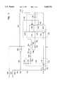
- FIG. 1is a schematic diagram illustrating an antifuse programming controller.
- FIGS. 2A-2Eare timing diagrams of voltages at selected nodes during programming of the antifuse programming controller of FIG. 1.
- FIG. 1is a schematic diagram illustrating a self-timed two phase antifuse programming controller operating on an antifuse 100 having a first and second terminal.
- the first terminal of antifuse 100is coupled to node 102 and receives a programming voltage at node 102.
- the second terminal of antifuse 100is coupled at node 104 to a switch 106 for interrupting a current through the antifuse 100.
- Switch 106is an n-channel metal-oxide-semiconductor (NMOS) field effect transistor (FET) having a drain terminal, a gate terminal, and a source terminal.
- NMOSmetal-oxide-semiconductor
- the drain terminal of switch 106is coupled to the second terminal of antifuse 100 at node 104.
- the gate terminal of switch 106receives a shutoff control voltage at node 108.
- the source terminal of switch 106is coupled at node 110 to a diode-connected NMOS current monitor FET 112 for monitoring the current through antifuse 100.
- a drain terminal and a gate terminal of current monitor FET 112are each coupled to node 110.
- a source terminal of NMOS current monitor FET 112is coupled to ground node 114.
- the antifuse programming controller of FIG. 1also comprises a first detector such as comparison circuit 116 for comparing the monitored current to a selected level of current such as a current trip point.
- comparison circuit 116comprises an NMOS first current mirror FET 118, a resistor 120, and a first comparator 122 which is more specifically an inverter.
- First current mirror FET 118replicates the current in current monitor FET 112 and scales this current by a first current mirroring ratio to provide a signal representative of the programming current flowing through the antifuse 100.
- the first current mirroring ratiois programmable, for example by switching in FETs in parallel with first current mirror FET 118, such that a current trip point is adjusted.
- a gate terminal of first current mirror FET 118is coupled at node 110 to each of the gate and drain terminals of current monitor FET 112.
- a source terminal of first current mirror FET 118is coupled to ground node 114.
- a drain terminal of first current mirror FET 118is coupled at node 124 to resistor 120. Resistor 120 receives the current replicated and sealed by first current mirror FET 118 and converts this current to a voltage at node 124.
- Resistor 120is coupled between a bias voltage, more particularly a power supply voltage at node 126, and the drain terminal of first current mirror FET 118.
- resistor 120is implemented as an integrated circuit resistor, such as a polysilicon resistor, a source/drain diffusion resistor, a well diffusion resistor, or a thin film resistor.
- resistor 120is implemented as an active device such as a FET.
- resistor 120is made either trimmable or programmable to adjust the current trip point.
- First comparator 122is an inverter, although other known voltage comparator topologies could also be used.
- First comparator 122has a first comparator input terminal coupled to node 124 where it receives the voltage derived by resistor 120 from the current replicated by first current mirror FET 118.
- First comparator 122provides an output voltage at a first comparator output terminal at node 128 in response to the voltage at node 124 compared to an input voltage trip point of first comparator 122.
- the antifuse programming controller of FIG. 1also comprises a second detector such as delay circuit 130 for turning off switch 106 to interrupt the current through antifuse 100 after adequate programming.
- Delay circuit 130comprises a second current mirror FET 132, a capacitor 134, a second comparator 136, and a shorting switch 138.
- Second current mirror FET 132replicates the current in current monitor FET 112, and scales this current by a second current mirroring ratio to provide a signal representative of the programming current flowing through the antifuse 100.
- the second current mirroring ratiois adjustable, for example by switching in FETs in parallel with second current mirror FET 132.
- a gate terminal of second current mirror FET 132is coupled at node 110 to each of the gate and drain terminals of current monitor FET 112.
- a source terminal of second current mirror FET 132is coupled to Found node 114.
- a drain terminal of second current mirror FET 132is coupled at node 140 to a first capacitor terminal of capacitor 134, which receives and integrates the current replicated and scaled by second current mirror FET 132, thereby producing a resulting voltage at node 140.
- a second capacitor terminal of capacitor 134is coupled at node 126 to the power supply voltage.
- Second comparator 136is an inverter, although other known voltage comparator topologies could also be used. Second comparator 136 has a second comparator input terminal coupled to and receiving the voltage at node 140 resulting from the integration by capacitor 134 of the current replicated by second current mirror FET 132. Second comparator 136 provides a binary logic output voltage at a flag node 142 based upon a comparison of the voltage at node 140 to an input voltage trip point of second comparator 136.
- Shorting switch 138is a p-channel metal-oxide-semiconductor (PMOS) FET having a source terminal coupled at node 126 to the second capacitor terminal, a drain terminal coupled at node 140 to the first capacitor terminal, and a gate terminal receiving a shorting control signal at node 146.
- Shorting switch 138is initially "on" during the time period when the antifuse 100 is not being programmed such that capacitor 134 is approximately discharged and the voltage at node 140 is approximately equal to the power supply voltage at node 126.
- the antifuse programming controller of FIG. 1also comprises logic circuits for turning on switch 106 until the current through antifuse 100 reaches a current trip point representing adequate programming of the antifuse 100. These logic circuits then initiate the delay period and turn off switch 106 after the delay period.
- the fast comparator output terminal at node 128is coupled by inverter 148 at node 150 to a first input terminal of 2-input NAND gate 158.
- Inverters 152 and 154couple the first capacitor terminal at node 140 to a second input terminal of NAND gate 158 at node 156.
- An output terminal of NAND gate 158provides the shorting control signal at node 146.
- NAND gate 158also has an enable input, referred to as EN, at program control node 160.
- the shorting control signal at node 146is also provided to a gate terminal of NMOS FET 162, which has a drain terminal coupled to the first capacitor terminal at node 140 and a source terminal coupled at node 164 to a drain terminal of FET 275.
- FET 275has a source terminal coupled to ground node 114 and a gate terminal coupled at flag node 142 to an output terminal of second comparator 136.
- the output terminal of second comparator 136is also coupled at flag node 142 to a first input of 2-input NOR gate 166.
- the second input of NOR gate 166is coupled to program control node 160.
- the output of NOR gate 166provides the shutoff control voltage at node 108. It is understood that other logic circuits could be substituted in FIG.
- flag node 142provides the output signal of the second comparator 136 to other circuitry as illustrated by an output connection 144.
- the other circuitrymay also provide control of program control node 160 to control programming current.
- FIGS. 2A, 2B, 2C, 2D and 2Eare timing diagrams illustrating time varying voltages at nodes 160, 110, 124, 140 and 142 respectively of the antifuse programming controller of FIG. 1 during programming of antifuse 100.
- Signal 260illustrates the voltage at program control node 160.
- Signals 210, 224, and 240illustrate the voltage at nodes 110, 124, and 140 respectively.
- Signal 242illustrates the voltage at flag node 142.
- antifuse programming controller of FIG. 1Before programming antifuse 100, the antifuse programming controller of FIG. 1 is placed in a known initial state, illustrated at time zero in FIGS. 2A-E.
- antifuse 100provides a high resistance between its first terminal at node 102 and its second terminal at node 104.
- the shutoff control voltage at node 108is low, thus switch 106 is off.
- Program control node 160is high, disabling NAND gate 158, forcing the shorting control signal at node 146 low, and turning on shorting switch 138.
- Capacitor 134is approximately discharged through shorting switch 138.
- FET 162is off and flag node 142 is low.
- program control node 160is transitioned from high to low at time t 1 .
- a programming voltage of approximately 10 voltsis applied to node 102 at time t 2 .
- the voltage transition of program control node 160 at time t 1turns on switch 106 and enables NAND gate 158.
- the shorting control signal at the output of NAND gate 158 at node 146remains low because nodes 124 and 140 are pulled high by resistor 120 and shorting switch 138 respectively.
- the voltage across the first and second terminals of antifuse 100is approximately equal to the difference between the programming voltage (approximately 10 volts) and a voltage slightly more positive than a FET threshold voltage (approximately 0.7 volt) of current monitor FET 112.
- This large voltageinduces breakdown of the dielectric of antifuse 100, thereby forming a conductive link between the first and second terminals of antifuse 100 and allowing current to flow through antifuse 100, switch 106, and current monitor FET 112.
- switch 106allows a programming current to flow through antifuse 100.
- the current flowing through current monitor FET 112is replicated and scaled by first current mirror FET 118 to form a current representative of the current flowing through antifuse 100.
- Resistor 120receives the current replicated and scaled by first current mirror FET 118, thereby lowering the voltage at node 124 toward the current trip point corresponding to the input voltage trip point of inverter 122.
- Shorting switch 138turns off upon initiation of the delay period at approximately time t 2 , and FET 162 turns on.
- Capacitor 134begins to charge by integrating a current received from second current mirror FET 132, which replicates and scales the current in current monitor FET 112 to form a current representative of the programming current flowing through antifuse 100.
- Capacitor 134lowers the voltage at node 140 as it integrates the current received at node 140 from second current mirror FET 132. Since the current received from second current mirror FET 132 is a function of the current through antifuse 100, the resulting delay period corresponds to an integral of the current through antifuse 100.
- the voltage across capacitor 134reaches a predetermined level at time t 3 , such that the voltage at node 140 is lowered below the input voltage trip point of second comparator 136, causing the logic value at the output terminal of the second comparator 136, at flag node 142, to transition from low to high at approximately time t 3 .
- FET 275turns on, thereby latching the voltage at node 140 such that it is approximately equal to the voltage at ground node 114.
- the shutoff control voltage at node 108transitions from high to low and switch 106 turns off, thereby inhibiting programming current from flowing through antifuse 100 and completing the programming of the antifuse 100.
- transition of the logic value at flag node 142 from low to highis used to flag control circuits at node 144 that programming of the antifuse 100 is complete, such that the programming current at node 160 may be stopped, and other antifuse 100 elements may be programmed after returning the program control node to a high logic level at time t 4 .
- the self-timing programming controllerminimizes the time required to optimally program an array of antifuse 100 elements.
- the current trip point and the delay periodare, in one embodiment, independently programmable. This allows increased flexibility to accommodate variations within the same fabrication process, or between different fabrication processes, which affect programming characteristics of the antifuse 100.
- the current trip pointis made adjustable, for example, by switching in FETs in parallel with first current mirror FET 118, thereby adjusting the first current mirroring ratio.
- resistor 120is made either trimmable or programmable to adjust the current trip point.
- the delay periodis made adjustable, for example, by switching in FETs in parallel with second current mirror FET 132, thereby adjusting the second current mirroring ratio.
- capacitor 134 valueis made programmable to adjust the delay period.
- the present inventionprovides a convenient method and apparatus for self-timed programming of an antifuse element, featuring monitoring which includes an independently programmable current trip point and delay period.
- the delay periodis a function of programming current through the antifuse 100.
- a higher resistance of antifuse 100results in a longer delay period and hence a longer programming time.
- Programming timeis optimized for individual antifuse 100 elements, and a flag signal is provided to other circuitry, on the same integrated circuit chip or external testing circuits. These other circuits may use this flag signal to monitor or control programming of an array of antifuse 100 elements, such that overall programming time for the array is reduced.
Landscapes
- Design And Manufacture Of Integrated Circuits (AREA)
Abstract
Description
Claims (24)
Priority Applications (2)
| Application Number | Priority Date | Filing Date | Title |
|---|---|---|---|
| US08/690,777US5668751A (en) | 1996-08-01 | 1996-08-01 | Antifuse programming method and apparatus |
| US08/858,945US5815429A (en) | 1996-08-01 | 1997-05-20 | Antifuse programming method and apparatus |
Applications Claiming Priority (1)
| Application Number | Priority Date | Filing Date | Title |
|---|---|---|---|
| US08/690,777US5668751A (en) | 1996-08-01 | 1996-08-01 | Antifuse programming method and apparatus |
Related Child Applications (1)
| Application Number | Title | Priority Date | Filing Date |
|---|---|---|---|
| US08/858,945ContinuationUS5815429A (en) | 1996-08-01 | 1997-05-20 | Antifuse programming method and apparatus |
Publications (1)
| Publication Number | Publication Date |
|---|---|
| US5668751Atrue US5668751A (en) | 1997-09-16 |
Family
ID=24773923
Family Applications (2)
| Application Number | Title | Priority Date | Filing Date |
|---|---|---|---|
| US08/690,777Expired - LifetimeUS5668751A (en) | 1996-08-01 | 1996-08-01 | Antifuse programming method and apparatus |
| US08/858,945Expired - LifetimeUS5815429A (en) | 1996-08-01 | 1997-05-20 | Antifuse programming method and apparatus |
Family Applications After (1)
| Application Number | Title | Priority Date | Filing Date |
|---|---|---|---|
| US08/858,945Expired - LifetimeUS5815429A (en) | 1996-08-01 | 1997-05-20 | Antifuse programming method and apparatus |
Country Status (1)
| Country | Link |
|---|---|
| US (2) | US5668751A (en) |
Cited By (12)
| Publication number | Priority date | Publication date | Assignee | Title |
|---|---|---|---|---|
| US5815429A (en)* | 1996-08-01 | 1998-09-29 | Micron Technology, Inc. | Antifuse programming method and apparatus |
| US5852379A (en)* | 1997-05-09 | 1998-12-22 | Integrated Silicon Solution Inc. | Fuse tunable, RC-generated pulse generator |
| US5962910A (en) | 1995-10-04 | 1999-10-05 | Actel Corporation | Metal-to-metal via-type antifuse |
| US6388305B1 (en) | 1999-12-17 | 2002-05-14 | International Business Machines Corporation | Electrically programmable antifuses and methods for forming the same |
| US6545928B1 (en) | 2001-09-25 | 2003-04-08 | Micron Technology, Inc. | Antifuse programming current limiter |
| US6973648B1 (en)* | 1999-01-27 | 2005-12-06 | International Business Machines Corporation | Method and device to process multidimensional array objects |
| US7825479B2 (en) | 2008-08-06 | 2010-11-02 | International Business Machines Corporation | Electrical antifuse having a multi-thickness dielectric layer |
| CN103377710A (en)* | 2012-04-23 | 2013-10-30 | 爱思开海力士有限公司 | Semiconductor device |
| FR2990291A1 (en)* | 2012-05-03 | 2013-11-08 | St Microelectronics Sa | METHOD FOR CONTROLLING THE CLASSIFICATION OF AN ANTIFUSE |
| CN112837733A (en)* | 2021-03-08 | 2021-05-25 | 中国科学院微电子研究所 | A resistive memory cell circuit, resistive memory and writing operation method |
| WO2022059176A1 (en)* | 2020-09-18 | 2022-03-24 | タワー パートナーズ セミコンダクター株式会社 | Semiconductor device |
| US20220266590A1 (en)* | 2021-02-22 | 2022-08-25 | Canon Kabushiki Kaisha | Element substrate, liquid discharge head, and liquid discharge apparatus |
Families Citing this family (13)
| Publication number | Priority date | Publication date | Assignee | Title |
|---|---|---|---|---|
| FR2787911B1 (en)* | 1998-12-23 | 2001-11-02 | St Microelectronics Sa | DIFFERENTIAL STRUCTURE OF MEMORY CELLS WITH UNIQUE PROGRAMMING IN CMOS TECHNOLOGY |
| US6346846B1 (en) | 1999-12-17 | 2002-02-12 | International Business Machines Corporation | Methods and apparatus for blowing and sensing antifuses |
| KR100400306B1 (en)* | 2000-12-29 | 2003-10-01 | 주식회사 하이닉스반도체 | Delay control circuit using anti-fuse |
| US6384666B1 (en) | 2001-03-23 | 2002-05-07 | International Business Machines Corporation | Antifuse latch device with controlled current programming and variable trip point |
| KR100756784B1 (en)* | 2001-12-28 | 2007-09-07 | 주식회사 하이닉스반도체 | Anti-fuse precharge circuit of semiconductor device |
| US6816427B2 (en) | 2002-11-27 | 2004-11-09 | Novocell Semiconductor, Inc. | Method of utilizing a plurality of voltage pulses to program non-volatile memory elements and related embedded memories |
| US6775197B2 (en)* | 2002-11-27 | 2004-08-10 | Novocell Semiconductor, Inc. | Non-volatile memory element integratable with standard CMOS circuitry and related programming methods and embedded memories |
| US6775171B2 (en)* | 2002-11-27 | 2004-08-10 | Novocell Semiconductor, Inc. | Method of utilizing voltage gradients to guide dielectric breakdowns for non-volatile memory elements and related embedded memories |
| US7498655B2 (en)* | 2006-03-28 | 2009-03-03 | Intel Corporation | Probe-based memory |
| US7538597B2 (en)* | 2007-08-13 | 2009-05-26 | Hong Kong Applied Science And Technology Research Institute Co. Ltd. | Fuse cell and method for programming the same |
| US8217684B2 (en)* | 2010-10-12 | 2012-07-10 | Magic Technologies, Inc. | Fast and accurate current driver with zero standby current and features for boost and temperature compensation for MRAM write circuit |
| CN107644659B (en)* | 2016-07-21 | 2020-08-18 | 中芯国际集成电路制造(上海)有限公司 | Multi-time-sequence programmable memory and electronic device |
| US11881274B2 (en) | 2021-11-15 | 2024-01-23 | Ememory Technology Inc. | Program control circuit for antifuse-type one time programming memory cell array |
Citations (10)
| Publication number | Priority date | Publication date | Assignee | Title |
|---|---|---|---|---|
| US5008855A (en)* | 1989-07-18 | 1991-04-16 | Actel Corporation | Method of programming anti-fuse element |
| US5250459A (en)* | 1992-04-14 | 1993-10-05 | Micron Technology, Inc. | Electrically programmable low resistive antifuse element |
| US5257222A (en)* | 1992-01-14 | 1993-10-26 | Micron Technology, Inc. | Antifuse programming by transistor snap-back |
| US5282158A (en)* | 1992-08-21 | 1994-01-25 | Micron Technology, Inc. | Transistor antifuse for a programmable ROM |
| US5301159A (en)* | 1993-02-05 | 1994-04-05 | Micron Technology, Inc. | Anti-fuse circuit and method wherein the read operation and programming operation are reversed |
| US5324681A (en)* | 1991-10-04 | 1994-06-28 | Micron Technology, Inc. | Method of making a 3-dimensional programmable antifuse for integrated circuits |
| US5331196A (en)* | 1991-08-19 | 1994-07-19 | Micron Technology, Inc. | One-time, voltage-programmable, logic element |
| US5371414A (en)* | 1993-05-26 | 1994-12-06 | Actel Corporation | Simultaneous multiple antifuse programming method |
| US5448187A (en)* | 1992-11-18 | 1995-09-05 | Gemplus Card International | Antifuse programming method and circuit which supplies a steady current after a programming voltage has dropped |
| US5495436A (en)* | 1995-01-13 | 1996-02-27 | Vlsi Technology, Inc. | Anti-fuse ROM programming circuit |
Family Cites Families (2)
| Publication number | Priority date | Publication date | Assignee | Title |
|---|---|---|---|---|
| US5689455A (en)* | 1995-08-31 | 1997-11-18 | Micron Technology, Inc. | Circuit for programming antifuse bits |
| US5668751A (en)* | 1996-08-01 | 1997-09-16 | Micron Technology, Inc. | Antifuse programming method and apparatus |
- 1996
- 1996-08-01USUS08/690,777patent/US5668751A/ennot_activeExpired - Lifetime
- 1997
- 1997-05-20USUS08/858,945patent/US5815429A/ennot_activeExpired - Lifetime
Patent Citations (10)
| Publication number | Priority date | Publication date | Assignee | Title |
|---|---|---|---|---|
| US5008855A (en)* | 1989-07-18 | 1991-04-16 | Actel Corporation | Method of programming anti-fuse element |
| US5331196A (en)* | 1991-08-19 | 1994-07-19 | Micron Technology, Inc. | One-time, voltage-programmable, logic element |
| US5324681A (en)* | 1991-10-04 | 1994-06-28 | Micron Technology, Inc. | Method of making a 3-dimensional programmable antifuse for integrated circuits |
| US5257222A (en)* | 1992-01-14 | 1993-10-26 | Micron Technology, Inc. | Antifuse programming by transistor snap-back |
| US5250459A (en)* | 1992-04-14 | 1993-10-05 | Micron Technology, Inc. | Electrically programmable low resistive antifuse element |
| US5282158A (en)* | 1992-08-21 | 1994-01-25 | Micron Technology, Inc. | Transistor antifuse for a programmable ROM |
| US5448187A (en)* | 1992-11-18 | 1995-09-05 | Gemplus Card International | Antifuse programming method and circuit which supplies a steady current after a programming voltage has dropped |
| US5301159A (en)* | 1993-02-05 | 1994-04-05 | Micron Technology, Inc. | Anti-fuse circuit and method wherein the read operation and programming operation are reversed |
| US5371414A (en)* | 1993-05-26 | 1994-12-06 | Actel Corporation | Simultaneous multiple antifuse programming method |
| US5495436A (en)* | 1995-01-13 | 1996-02-27 | Vlsi Technology, Inc. | Anti-fuse ROM programming circuit |
Cited By (19)
| Publication number | Priority date | Publication date | Assignee | Title |
|---|---|---|---|---|
| US5962910A (en) | 1995-10-04 | 1999-10-05 | Actel Corporation | Metal-to-metal via-type antifuse |
| US5815429A (en)* | 1996-08-01 | 1998-09-29 | Micron Technology, Inc. | Antifuse programming method and apparatus |
| US5852379A (en)* | 1997-05-09 | 1998-12-22 | Integrated Silicon Solution Inc. | Fuse tunable, RC-generated pulse generator |
| US6973648B1 (en)* | 1999-01-27 | 2005-12-06 | International Business Machines Corporation | Method and device to process multidimensional array objects |
| US7496923B2 (en) | 1999-01-27 | 2009-02-24 | International Business Machines Corporation | Method and device to process multidimensional array objects |
| US6388305B1 (en) | 1999-12-17 | 2002-05-14 | International Business Machines Corporation | Electrically programmable antifuses and methods for forming the same |
| US6812122B2 (en) | 1999-12-17 | 2004-11-02 | International Business Machines Corporation | Method for forming a voltage programming element |
| US6545928B1 (en) | 2001-09-25 | 2003-04-08 | Micron Technology, Inc. | Antifuse programming current limiter |
| US7825479B2 (en) | 2008-08-06 | 2010-11-02 | International Business Machines Corporation | Electrical antifuse having a multi-thickness dielectric layer |
| CN103377710A (en)* | 2012-04-23 | 2013-10-30 | 爱思开海力士有限公司 | Semiconductor device |
| CN103377710B (en)* | 2012-04-23 | 2018-08-07 | 爱思开海力士有限公司 | Semiconductor devices |
| FR2990291A1 (en)* | 2012-05-03 | 2013-11-08 | St Microelectronics Sa | METHOD FOR CONTROLLING THE CLASSIFICATION OF AN ANTIFUSE |
| US9142318B2 (en) | 2012-05-03 | 2015-09-22 | Stmicroelectronics Sa | Method for controlling the breakdown of an antifuse memory cell |
| US9564242B2 (en) | 2012-05-03 | 2017-02-07 | Stmicroelectronics Sa | Method for controlling the breakdown of an antifuse memory cell |
| WO2022059176A1 (en)* | 2020-09-18 | 2022-03-24 | タワー パートナーズ セミコンダクター株式会社 | Semiconductor device |
| US12260922B2 (en) | 2020-09-18 | 2025-03-25 | Tower Partners Semiconductor Co., Ltd. | Semiconductor device for writing to a storage element |
| US20220266590A1 (en)* | 2021-02-22 | 2022-08-25 | Canon Kabushiki Kaisha | Element substrate, liquid discharge head, and liquid discharge apparatus |
| US11975536B2 (en)* | 2021-02-22 | 2024-05-07 | Canon Kabushiki Kaisha | Element substrate, liquid discharge head, and liquid discharge apparatus |
| CN112837733A (en)* | 2021-03-08 | 2021-05-25 | 中国科学院微电子研究所 | A resistive memory cell circuit, resistive memory and writing operation method |
Also Published As
| Publication number | Publication date |
|---|---|
| US5815429A (en) | 1998-09-29 |
Similar Documents
| Publication | Publication Date | Title |
|---|---|---|
| US5668751A (en) | Antifuse programming method and apparatus | |
| US5831923A (en) | Antifuse detect circuit | |
| EP0157905B1 (en) | Semiconductor device | |
| EP0323643B1 (en) | Semiconductor integrated circuit with a circuit limiting an input voltage to a predetermined voltage | |
| US5896041A (en) | Method and apparatus for programming anti-fuses using internally generated programming voltage | |
| US6266794B1 (en) | Circuit and method for testing an integrated circuit | |
| EP0399240A2 (en) | Semiconductor memory device | |
| US6545926B2 (en) | Antifuse address detecting circuit programmable by applying a high voltage and semiconductor integrated circuit device provided with the same | |
| KR940009349B1 (en) | Semiconductor device having a temperature detection circuit | |
| US4849847A (en) | Power supply switch for wafer scale applications | |
| JP2881729B2 (en) | Burn-in detection circuit for semiconductor memory | |
| US20020000582A1 (en) | Semiconductor device including voltage down converter allowing tuning in short period of time and reduction of chip area | |
| US10566070B2 (en) | Electronic device with a fuse read mechanism | |
| US6549063B1 (en) | Evaluation circuit for an anti-fuse | |
| US6515934B2 (en) | Semiconductor device including internal potential generating circuit allowing tuning in short period of time and reduction of chip area | |
| US6606264B2 (en) | Programmable circuit and its method of operation | |
| US6903986B2 (en) | Method and apparatus for improving the reliability of the reading of integrated circuit fuses | |
| JP3745875B2 (en) | Burn-in stress control circuit for semiconductor memory device | |
| JPH03289568A (en) | Voltage detector | |
| KR950008454B1 (en) | Internal source voltage generating circuit |
Legal Events
| Date | Code | Title | Description |
|---|---|---|---|
| AS | Assignment | Owner name:MICRON TECHNOLOGY, INC., IDAHO Free format text:ASSIGNMENT OF ASSIGNORS INTEREST;ASSIGNORS:SHER, JOSEPH C.;KEETH, BRENT;REEL/FRAME:008155/0974;SIGNING DATES FROM 19960726 TO 19960730 | |
| FEPP | Fee payment procedure | Free format text:PAYOR NUMBER ASSIGNED (ORIGINAL EVENT CODE: ASPN); ENTITY STATUS OF PATENT OWNER: LARGE ENTITY | |
| STCF | Information on status: patent grant | Free format text:PATENTED CASE | |
| CC | Certificate of correction | ||
| FPAY | Fee payment | Year of fee payment:4 | |
| FPAY | Fee payment | Year of fee payment:8 | |
| FPAY | Fee payment | Year of fee payment:12 | |
| AS | Assignment | Owner name:MORGAN STANLEY SENIOR FUNDING, INC., AS COLLATERAL AGENT, MARYLAND Free format text:PATENT SECURITY AGREEMENT;ASSIGNOR:MICRON TECHNOLOGY, INC.;REEL/FRAME:038954/0001 Effective date:20160426 Owner name:MORGAN STANLEY SENIOR FUNDING, INC., AS COLLATERAL Free format text:PATENT SECURITY AGREEMENT;ASSIGNOR:MICRON TECHNOLOGY, INC.;REEL/FRAME:038954/0001 Effective date:20160426 | |
| AS | Assignment | Owner name:MICRON TECHNOLOGY, INC., IDAHO Free format text:RELEASE BY SECURED PARTY;ASSIGNOR:U.S. BANK NATIONAL ASSOCIATION, AS COLLATERAL AGENT;REEL/FRAME:047243/0001 Effective date:20180629 | |
| AS | Assignment | Owner name:MICRON TECHNOLOGY, INC., IDAHO Free format text:RELEASE BY SECURED PARTY;ASSIGNOR:MORGAN STANLEY SENIOR FUNDING, INC., AS COLLATERAL AGENT;REEL/FRAME:050937/0001 Effective date:20190731 |