US5668405A - Semiconductor device with a film carrier tape - Google Patents
Semiconductor device with a film carrier tapeDownload PDFInfo
- Publication number
- US5668405A US5668405AUS08/528,244US52824495AUS5668405AUS 5668405 AUS5668405 AUS 5668405AUS 52824495 AUS52824495 AUS 52824495AUS 5668405 AUS5668405 AUS 5668405A
- Authority
- US
- United States
- Prior art keywords
- semiconductor device
- land
- hole
- bump
- base film
- Prior art date
- Legal status (The legal status is an assumption and is not a legal conclusion. Google has not performed a legal analysis and makes no representation as to the accuracy of the status listed.)
- Expired - Fee Related
Links
Images


Classifications
- H—ELECTRICITY
- H01—ELECTRIC ELEMENTS
- H01L—SEMICONDUCTOR DEVICES NOT COVERED BY CLASS H10
- H01L24/00—Arrangements for connecting or disconnecting semiconductor or solid-state bodies; Methods or apparatus related thereto
- H01L24/01—Means for bonding being attached to, or being formed on, the surface to be connected, e.g. chip-to-package, die-attach, "first-level" interconnects; Manufacturing methods related thereto
- H01L24/50—Tape automated bonding [TAB] connectors, i.e. film carriers; Manufacturing methods related thereto
- H—ELECTRICITY
- H01—ELECTRIC ELEMENTS
- H01L—SEMICONDUCTOR DEVICES NOT COVERED BY CLASS H10
- H01L23/00—Details of semiconductor or other solid state devices
- H01L23/28—Encapsulations, e.g. encapsulating layers, coatings, e.g. for protection
- H01L23/31—Encapsulations, e.g. encapsulating layers, coatings, e.g. for protection characterised by the arrangement or shape
- H01L23/3107—Encapsulations, e.g. encapsulating layers, coatings, e.g. for protection characterised by the arrangement or shape the device being completely enclosed
- H—ELECTRICITY
- H01—ELECTRIC ELEMENTS
- H01L—SEMICONDUCTOR DEVICES NOT COVERED BY CLASS H10
- H01L23/00—Details of semiconductor or other solid state devices
- H01L23/48—Arrangements for conducting electric current to or from the solid state body in operation, e.g. leads, terminal arrangements ; Selection of materials therefor
- H01L23/488—Arrangements for conducting electric current to or from the solid state body in operation, e.g. leads, terminal arrangements ; Selection of materials therefor consisting of soldered or bonded constructions
- H01L23/495—Lead-frames or other flat leads
- H01L23/49572—Lead-frames or other flat leads consisting of thin flexible metallic tape with or without a film carrier
- H—ELECTRICITY
- H01—ELECTRIC ELEMENTS
- H01L—SEMICONDUCTOR DEVICES NOT COVERED BY CLASS H10
- H01L23/00—Details of semiconductor or other solid state devices
- H01L23/48—Arrangements for conducting electric current to or from the solid state body in operation, e.g. leads, terminal arrangements ; Selection of materials therefor
- H01L23/488—Arrangements for conducting electric current to or from the solid state body in operation, e.g. leads, terminal arrangements ; Selection of materials therefor consisting of soldered or bonded constructions
- H01L23/498—Leads, i.e. metallisations or lead-frames on insulating substrates, e.g. chip carriers
- H01L23/49811—Additional leads joined to the metallisation on the insulating substrate, e.g. pins, bumps, wires, flat leads
- H01L23/49816—Spherical bumps on the substrate for external connection, e.g. ball grid arrays [BGA]
- H—ELECTRICITY
- H01—ELECTRIC ELEMENTS
- H01L—SEMICONDUCTOR DEVICES NOT COVERED BY CLASS H10
- H01L23/00—Details of semiconductor or other solid state devices
- H01L23/48—Arrangements for conducting electric current to or from the solid state body in operation, e.g. leads, terminal arrangements ; Selection of materials therefor
- H01L23/488—Arrangements for conducting electric current to or from the solid state body in operation, e.g. leads, terminal arrangements ; Selection of materials therefor consisting of soldered or bonded constructions
- H01L23/498—Leads, i.e. metallisations or lead-frames on insulating substrates, e.g. chip carriers
- H01L23/49827—Via connections through the substrates, e.g. pins going through the substrate, coaxial cables
- H—ELECTRICITY
- H05—ELECTRIC TECHNIQUES NOT OTHERWISE PROVIDED FOR
- H05K—PRINTED CIRCUITS; CASINGS OR CONSTRUCTIONAL DETAILS OF ELECTRIC APPARATUS; MANUFACTURE OF ASSEMBLAGES OF ELECTRICAL COMPONENTS
- H05K3/00—Apparatus or processes for manufacturing printed circuits
- H05K3/36—Assembling printed circuits with other printed circuits
- H05K3/361—Assembling flexible printed circuits with other printed circuits
- H05K3/363—Assembling flexible printed circuits with other printed circuits by soldering
- H—ELECTRICITY
- H01—ELECTRIC ELEMENTS
- H01L—SEMICONDUCTOR DEVICES NOT COVERED BY CLASS H10
- H01L2224/00—Indexing scheme for arrangements for connecting or disconnecting semiconductor or solid-state bodies and methods related thereto as covered by H01L24/00
- H01L2224/01—Means for bonding being attached to, or being formed on, the surface to be connected, e.g. chip-to-package, die-attach, "first-level" interconnects; Manufacturing methods related thereto
- H01L2224/10—Bump connectors; Manufacturing methods related thereto
- H01L2224/15—Structure, shape, material or disposition of the bump connectors after the connecting process
- H01L2224/16—Structure, shape, material or disposition of the bump connectors after the connecting process of an individual bump connector
- H—ELECTRICITY
- H01—ELECTRIC ELEMENTS
- H01L—SEMICONDUCTOR DEVICES NOT COVERED BY CLASS H10
- H01L2224/00—Indexing scheme for arrangements for connecting or disconnecting semiconductor or solid-state bodies and methods related thereto as covered by H01L24/00
- H01L2224/01—Means for bonding being attached to, or being formed on, the surface to be connected, e.g. chip-to-package, die-attach, "first-level" interconnects; Manufacturing methods related thereto
- H01L2224/42—Wire connectors; Manufacturing methods related thereto
- H01L2224/47—Structure, shape, material or disposition of the wire connectors after the connecting process
- H01L2224/48—Structure, shape, material or disposition of the wire connectors after the connecting process of an individual wire connector
- H01L2224/4805—Shape
- H01L2224/4809—Loop shape
- H01L2224/48091—Arched
- H—ELECTRICITY
- H01—ELECTRIC ELEMENTS
- H01L—SEMICONDUCTOR DEVICES NOT COVERED BY CLASS H10
- H01L2224/00—Indexing scheme for arrangements for connecting or disconnecting semiconductor or solid-state bodies and methods related thereto as covered by H01L24/00
- H01L2224/01—Means for bonding being attached to, or being formed on, the surface to be connected, e.g. chip-to-package, die-attach, "first-level" interconnects; Manufacturing methods related thereto
- H01L2224/50—Tape automated bonding [TAB] connectors, i.e. film carriers; Manufacturing methods related thereto
- H—ELECTRICITY
- H01—ELECTRIC ELEMENTS
- H01L—SEMICONDUCTOR DEVICES NOT COVERED BY CLASS H10
- H01L2224/00—Indexing scheme for arrangements for connecting or disconnecting semiconductor or solid-state bodies and methods related thereto as covered by H01L24/00
- H01L2224/73—Means for bonding being of different types provided for in two or more of groups H01L2224/10, H01L2224/18, H01L2224/26, H01L2224/34, H01L2224/42, H01L2224/50, H01L2224/63, H01L2224/71
- H01L2224/732—Location after the connecting process
- H01L2224/73251—Location after the connecting process on different surfaces
- H01L2224/73263—Layer and strap connectors
- H—ELECTRICITY
- H01—ELECTRIC ELEMENTS
- H01L—SEMICONDUCTOR DEVICES NOT COVERED BY CLASS H10
- H01L24/00—Arrangements for connecting or disconnecting semiconductor or solid-state bodies; Methods or apparatus related thereto
- H01L24/01—Means for bonding being attached to, or being formed on, the surface to be connected, e.g. chip-to-package, die-attach, "first-level" interconnects; Manufacturing methods related thereto
- H01L24/42—Wire connectors; Manufacturing methods related thereto
- H01L24/47—Structure, shape, material or disposition of the wire connectors after the connecting process
- H01L24/48—Structure, shape, material or disposition of the wire connectors after the connecting process of an individual wire connector
- H—ELECTRICITY
- H01—ELECTRIC ELEMENTS
- H01L—SEMICONDUCTOR DEVICES NOT COVERED BY CLASS H10
- H01L2924/00—Indexing scheme for arrangements or methods for connecting or disconnecting semiconductor or solid-state bodies as covered by H01L24/00
- H01L2924/0001—Technical content checked by a classifier
- H01L2924/00014—Technical content checked by a classifier the subject-matter covered by the group, the symbol of which is combined with the symbol of this group, being disclosed without further technical details
- H—ELECTRICITY
- H01—ELECTRIC ELEMENTS
- H01L—SEMICONDUCTOR DEVICES NOT COVERED BY CLASS H10
- H01L2924/00—Indexing scheme for arrangements or methods for connecting or disconnecting semiconductor or solid-state bodies as covered by H01L24/00
- H01L2924/01—Chemical elements
- H01L2924/01005—Boron [B]
- H—ELECTRICITY
- H01—ELECTRIC ELEMENTS
- H01L—SEMICONDUCTOR DEVICES NOT COVERED BY CLASS H10
- H01L2924/00—Indexing scheme for arrangements or methods for connecting or disconnecting semiconductor or solid-state bodies as covered by H01L24/00
- H01L2924/01—Chemical elements
- H01L2924/01013—Aluminum [Al]
- H—ELECTRICITY
- H01—ELECTRIC ELEMENTS
- H01L—SEMICONDUCTOR DEVICES NOT COVERED BY CLASS H10
- H01L2924/00—Indexing scheme for arrangements or methods for connecting or disconnecting semiconductor or solid-state bodies as covered by H01L24/00
- H01L2924/01—Chemical elements
- H01L2924/01029—Copper [Cu]
- H—ELECTRICITY
- H01—ELECTRIC ELEMENTS
- H01L—SEMICONDUCTOR DEVICES NOT COVERED BY CLASS H10
- H01L2924/00—Indexing scheme for arrangements or methods for connecting or disconnecting semiconductor or solid-state bodies as covered by H01L24/00
- H01L2924/01—Chemical elements
- H01L2924/01033—Arsenic [As]
- H—ELECTRICITY
- H01—ELECTRIC ELEMENTS
- H01L—SEMICONDUCTOR DEVICES NOT COVERED BY CLASS H10
- H01L2924/00—Indexing scheme for arrangements or methods for connecting or disconnecting semiconductor or solid-state bodies as covered by H01L24/00
- H01L2924/01—Chemical elements
- H01L2924/01057—Lanthanum [La]
- H—ELECTRICITY
- H01—ELECTRIC ELEMENTS
- H01L—SEMICONDUCTOR DEVICES NOT COVERED BY CLASS H10
- H01L2924/00—Indexing scheme for arrangements or methods for connecting or disconnecting semiconductor or solid-state bodies as covered by H01L24/00
- H01L2924/01—Chemical elements
- H01L2924/01075—Rhenium [Re]
- H—ELECTRICITY
- H01—ELECTRIC ELEMENTS
- H01L—SEMICONDUCTOR DEVICES NOT COVERED BY CLASS H10
- H01L2924/00—Indexing scheme for arrangements or methods for connecting or disconnecting semiconductor or solid-state bodies as covered by H01L24/00
- H01L2924/01—Chemical elements
- H01L2924/01078—Platinum [Pt]
- H—ELECTRICITY
- H01—ELECTRIC ELEMENTS
- H01L—SEMICONDUCTOR DEVICES NOT COVERED BY CLASS H10
- H01L2924/00—Indexing scheme for arrangements or methods for connecting or disconnecting semiconductor or solid-state bodies as covered by H01L24/00
- H01L2924/01—Chemical elements
- H01L2924/01079—Gold [Au]
- H—ELECTRICITY
- H01—ELECTRIC ELEMENTS
- H01L—SEMICONDUCTOR DEVICES NOT COVERED BY CLASS H10
- H01L2924/00—Indexing scheme for arrangements or methods for connecting or disconnecting semiconductor or solid-state bodies as covered by H01L24/00
- H01L2924/01—Chemical elements
- H01L2924/01082—Lead [Pb]
- H—ELECTRICITY
- H01—ELECTRIC ELEMENTS
- H01L—SEMICONDUCTOR DEVICES NOT COVERED BY CLASS H10
- H01L2924/00—Indexing scheme for arrangements or methods for connecting or disconnecting semiconductor or solid-state bodies as covered by H01L24/00
- H01L2924/013—Alloys
- H01L2924/0132—Binary Alloys
- H01L2924/01322—Eutectic Alloys, i.e. obtained by a liquid transforming into two solid phases
- H—ELECTRICITY
- H01—ELECTRIC ELEMENTS
- H01L—SEMICONDUCTOR DEVICES NOT COVERED BY CLASS H10
- H01L2924/00—Indexing scheme for arrangements or methods for connecting or disconnecting semiconductor or solid-state bodies as covered by H01L24/00
- H01L2924/10—Details of semiconductor or other solid state devices to be connected
- H01L2924/11—Device type
- H01L2924/12—Passive devices, e.g. 2 terminal devices
- H01L2924/1204—Optical Diode
- H01L2924/12042—LASER
- H—ELECTRICITY
- H01—ELECTRIC ELEMENTS
- H01L—SEMICONDUCTOR DEVICES NOT COVERED BY CLASS H10
- H01L2924/00—Indexing scheme for arrangements or methods for connecting or disconnecting semiconductor or solid-state bodies as covered by H01L24/00
- H01L2924/10—Details of semiconductor or other solid state devices to be connected
- H01L2924/11—Device type
- H01L2924/14—Integrated circuits
- H—ELECTRICITY
- H01—ELECTRIC ELEMENTS
- H01L—SEMICONDUCTOR DEVICES NOT COVERED BY CLASS H10
- H01L2924/00—Indexing scheme for arrangements or methods for connecting or disconnecting semiconductor or solid-state bodies as covered by H01L24/00
- H01L2924/15—Details of package parts other than the semiconductor or other solid state devices to be connected
- H01L2924/151—Die mounting substrate
- H01L2924/1515—Shape
- H01L2924/15153—Shape the die mounting substrate comprising a recess for hosting the device
- H—ELECTRICITY
- H01—ELECTRIC ELEMENTS
- H01L—SEMICONDUCTOR DEVICES NOT COVERED BY CLASS H10
- H01L2924/00—Indexing scheme for arrangements or methods for connecting or disconnecting semiconductor or solid-state bodies as covered by H01L24/00
- H01L2924/15—Details of package parts other than the semiconductor or other solid state devices to be connected
- H01L2924/151—Die mounting substrate
- H01L2924/15165—Monolayer substrate
- H—ELECTRICITY
- H01—ELECTRIC ELEMENTS
- H01L—SEMICONDUCTOR DEVICES NOT COVERED BY CLASS H10
- H01L2924/00—Indexing scheme for arrangements or methods for connecting or disconnecting semiconductor or solid-state bodies as covered by H01L24/00
- H01L2924/15—Details of package parts other than the semiconductor or other solid state devices to be connected
- H01L2924/151—Die mounting substrate
- H01L2924/1517—Multilayer substrate
- H—ELECTRICITY
- H01—ELECTRIC ELEMENTS
- H01L—SEMICONDUCTOR DEVICES NOT COVERED BY CLASS H10
- H01L2924/00—Indexing scheme for arrangements or methods for connecting or disconnecting semiconductor or solid-state bodies as covered by H01L24/00
- H01L2924/15—Details of package parts other than the semiconductor or other solid state devices to be connected
- H01L2924/151—Die mounting substrate
- H01L2924/153—Connection portion
- H01L2924/1531—Connection portion the connection portion being formed only on the surface of the substrate opposite to the die mounting surface
- H01L2924/15311—Connection portion the connection portion being formed only on the surface of the substrate opposite to the die mounting surface being a ball array, e.g. BGA
- H—ELECTRICITY
- H01—ELECTRIC ELEMENTS
- H01L—SEMICONDUCTOR DEVICES NOT COVERED BY CLASS H10
- H01L2924/00—Indexing scheme for arrangements or methods for connecting or disconnecting semiconductor or solid-state bodies as covered by H01L24/00
- H01L2924/15—Details of package parts other than the semiconductor or other solid state devices to be connected
- H01L2924/151—Die mounting substrate
- H01L2924/156—Material
- H01L2924/15786—Material with a principal constituent of the material being a non metallic, non metalloid inorganic material
- H01L2924/15787—Ceramics, e.g. crystalline carbides, nitrides or oxides
- H—ELECTRICITY
- H01—ELECTRIC ELEMENTS
- H01L—SEMICONDUCTOR DEVICES NOT COVERED BY CLASS H10
- H01L2924/00—Indexing scheme for arrangements or methods for connecting or disconnecting semiconductor or solid-state bodies as covered by H01L24/00
- H01L2924/15—Details of package parts other than the semiconductor or other solid state devices to be connected
- H01L2924/161—Cap
- H01L2924/1615—Shape
- H01L2924/16152—Cap comprising a cavity for hosting the device, e.g. U-shaped cap
- H—ELECTRICITY
- H01—ELECTRIC ELEMENTS
- H01L—SEMICONDUCTOR DEVICES NOT COVERED BY CLASS H10
- H01L2924/00—Indexing scheme for arrangements or methods for connecting or disconnecting semiconductor or solid-state bodies as covered by H01L24/00
- H01L2924/15—Details of package parts other than the semiconductor or other solid state devices to be connected
- H01L2924/181—Encapsulation
- H—ELECTRICITY
- H01—ELECTRIC ELEMENTS
- H01L—SEMICONDUCTOR DEVICES NOT COVERED BY CLASS H10
- H01L2924/00—Indexing scheme for arrangements or methods for connecting or disconnecting semiconductor or solid-state bodies as covered by H01L24/00
- H01L2924/30—Technical effects
- H01L2924/35—Mechanical effects
- H01L2924/351—Thermal stress
- H—ELECTRICITY
- H05—ELECTRIC TECHNIQUES NOT OTHERWISE PROVIDED FOR
- H05K—PRINTED CIRCUITS; CASINGS OR CONSTRUCTIONAL DETAILS OF ELECTRIC APPARATUS; MANUFACTURE OF ASSEMBLAGES OF ELECTRICAL COMPONENTS
- H05K1/00—Printed circuits
- H05K1/02—Details
- H05K1/0266—Marks, test patterns or identification means
- H05K1/0269—Marks, test patterns or identification means for visual or optical inspection
- H—ELECTRICITY
- H05—ELECTRIC TECHNIQUES NOT OTHERWISE PROVIDED FOR
- H05K—PRINTED CIRCUITS; CASINGS OR CONSTRUCTIONAL DETAILS OF ELECTRIC APPARATUS; MANUFACTURE OF ASSEMBLAGES OF ELECTRICAL COMPONENTS
- H05K2201/00—Indexing scheme relating to printed circuits covered by H05K1/00
- H05K2201/03—Conductive materials
- H05K2201/0332—Structure of the conductor
- H05K2201/0388—Other aspects of conductors
- H05K2201/0394—Conductor crossing over a hole in the substrate or a gap between two separate substrate parts
- H—ELECTRICITY
- H05—ELECTRIC TECHNIQUES NOT OTHERWISE PROVIDED FOR
- H05K—PRINTED CIRCUITS; CASINGS OR CONSTRUCTIONAL DETAILS OF ELECTRIC APPARATUS; MANUFACTURE OF ASSEMBLAGES OF ELECTRICAL COMPONENTS
- H05K2201/00—Indexing scheme relating to printed circuits covered by H05K1/00
- H05K2201/09—Shape and layout
- H05K2201/09209—Shape and layout details of conductors
- H05K2201/09654—Shape and layout details of conductors covering at least two types of conductors provided for in H05K2201/09218 - H05K2201/095
- H05K2201/0969—Apertured conductors
- H—ELECTRICITY
- H05—ELECTRIC TECHNIQUES NOT OTHERWISE PROVIDED FOR
- H05K—PRINTED CIRCUITS; CASINGS OR CONSTRUCTIONAL DETAILS OF ELECTRIC APPARATUS; MANUFACTURE OF ASSEMBLAGES OF ELECTRICAL COMPONENTS
- H05K2201/00—Indexing scheme relating to printed circuits covered by H05K1/00
- H05K2201/10—Details of components or other objects attached to or integrated in a printed circuit board
- H05K2201/10613—Details of electrical connections of non-printed components, e.g. special leads
- H05K2201/10621—Components characterised by their electrical contacts
- H05K2201/10681—Tape Carrier Package [TCP]; Flexible sheet connector
- H—ELECTRICITY
- H05—ELECTRIC TECHNIQUES NOT OTHERWISE PROVIDED FOR
- H05K—PRINTED CIRCUITS; CASINGS OR CONSTRUCTIONAL DETAILS OF ELECTRIC APPARATUS; MANUFACTURE OF ASSEMBLAGES OF ELECTRICAL COMPONENTS
- H05K2201/00—Indexing scheme relating to printed circuits covered by H05K1/00
- H05K2201/10—Details of components or other objects attached to or integrated in a printed circuit board
- H05K2201/10613—Details of electrical connections of non-printed components, e.g. special leads
- H05K2201/10621—Components characterised by their electrical contacts
- H05K2201/10734—Ball grid array [BGA]; Bump grid array
Definitions
- This inventionrelates to a semiconductor device, and more particularly to, a semiconductor device in which a semiconductor integrated circuit is mounted on a film carrier tape.
- a method for making a conventional semiconductor device with a film carrier tapeis as follows:
- a base filmwhich is made of polyimide, polyester, glass-epoxy or the like and in which sprocket holes for carrying and positioning and device holes for placing semiconductor devices are opened.
- a metal foil of copper or the likeis adhered to the base film by adhesives, thereafter etching the metal foil to form leads with given shapes and pads for electrical selection.
- the inner lead bonding (hereinafter referred to as "ILB") of the leads extending in the device hole of the film carrier tape to bumps formed on electrodes of an IC chipis carried out by a thermo-compression method of eutectic method.
- an electrical selection test and BTburn-in test
- the leadsare cut to desirable lengths to carry out outer lead bonding (hereinafter referred to as "OLB").
- a method of leaving insulating film composing the film carrier tape on the outer end of the outer leadsis often employed. Thereafter, mounting is carried out, for example, by OLB of the leads to the bonding pads on a printed substrate.
- the outer re-flow pitch in QFP which can be re-flownis limited to about 0.4 mm.
- this BGA packageuses a multilayer printed substrate, it can employ a ceramic substrate or film carrier tape.
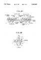
- FIG. 1Ais a cross sectional view showing the BGA package
- FIG. 1Bis a enlarged cross sectional view showing a part of the BGA package which is indicated by a circle B in FIG. 1A.
- a copper-foil wiring 3 formed on a base film 2is connected to a land 3b formed under the base film and a through-hole plating 3d, i.e., the film carrier tape is composed by so called a two layers-two metal technique.
- a solder bump as an outer terminalis formed by providing a solder ball 11.
- a bump 1b on a semiconductor IC chip 1is connected to the inner lead 3a of the copper-foil wiring 3.
- a reinforcing plate 13is pasted by an adhesive 12 thereon to reinforce the film carrier tape, and a heat spreader 15 is pasted by adhesives 10, 14 on the semiconductor IC chip 1 and reinforcing plate 13 to reduce the heat resistance.
- solder pasteis provided with the pads on the mounting substrate, thereafter adhering to the solder ball 11 to mount it.
- the cost making thereofincreases to about five to ten times as compared with a film carrier tape made by a conventional three layers-one metal technique, since the film carrier tape thereof is made by the two layers-two metal technique.
- the film carrier tape made by the two layers-two metal techniqueis subject to lack of mechanical strength caused by the tape thickness of about 50 to 70 ⁇ m, thereby causing an undulation or bend of the substrate to reduce the easiness of mounting which is a excellent property of BGA. Therefore, it needs the reinforcing plate 13 for reinforcing the mechanical strength.
- the solder ball 11 as a connecting means to the substratecan not be checked with the naked eye after mounting.
- the mounting statecan be optionally checked by the other way, for example, a x-ray instrument, it is not a proper way for the mass production and it will result in a package with high cost.
- the first prior artlacks in the easiness of mounting and it is not multipurpose to various use.
- Japanese Patent Applications Laid-Open No. 61-51945 and 1-258454disclose another type of semiconductor device in which the state of soldering after mounting can be checked on a package substrate.
- FIGS. 2A and 2Bshows the semiconductor device disclosed in Japanese Patent Applications Laid-Open No. 1-258454 (hereinafter referred to as "second prior art").
- the semiconductor deviceis called LGA (Land Grid Array). It uses a rigid substrate as a package substrate 16 which is similar to that of the above-mentioned standard BGA package, forming a copper-foil wiring on and under the substrate 16, connecting between lands 17a and 17b which are formed in a grid form on and under the substrate by through-hole plating 17c, further compressing and bonding a copper plate to the center of the backside of the substrate. Solder plating 19 is provided with the land 17b.
- a semiconductor IC chip 1is adhered by an adhesive 10 to the concave portion formed in the center of the substrate.
- the semiconductor IC chip 1 and the copper-foil wiring 17are connected by a bonding wire 20, thereafter being sealed with sealing resin 5.
- solder pasteis previously coated to the pads on eh mounting substrate 9 by a screen printing method or the like, positioning and mounting the LGA package to the mounting substrate 9 and re-flowing the solder.
- solder 21 on the mounting substrate 9climbs up passing the through-hole to form climbed solder 21a.
- the solder junction between the mounting substrate 9 and the package substrate 16can be checked through the climbed solder 21.
- Japanese Patent Application Laid-Open No. 63-34936discloses a LGA package with a film carrier tape (hereinafter referred to as "third prior art").
- This packageis made by forming a copper-foil wiring on the film carrier tape, forming a land on the backside of the tape, connecting them by a through-hole and carrying out ILB of a semiconductor IC chip to the inner leads of the copper-foil wiring.
- this packageis mounted after solder paste is previously coated to a mounting substrate.
- the first and third prior artshave a problem that the state of the solder junction can not be observed after mounting.
- the package costbecomes higher since the package employs a film carrier tape of two layers-two metals structure, and the package lacks in mass producibility since it needs the reinforcing plate 13.
- this packagelacks in mass producibility in that it uses a rigid substrate as a substrate, as compared with a package using a film carrier tape. Further, in this package structure, the through-hole plating 17c, the solder plating 19 on the land 17b and the copper plate 18 for maintaining the level even to the soldered portion after mounting are required. Thus, the package structure is complex, and the package cost becomes higher.
- solder required in mountingis provided not with the package but with the mounting substrate.
- the solder of solder paste or the likeis supplied to a screen printing method.
- the pitch P3 between the lands 17bis 1.27 mm
- the diameter of the landis to be about 0.5 to 0.6 mm.
- the gap between the package and the mounting substrate after mountingneeds to be about 0.5 to 1.0 mm in order to securely connect therebetween and reduce a thermal stress occurred therebetween by the difference in their thermal expansion coefficients. Therefore, it is necessary to supply solder paste to have a thickness of 1.0 to 1.5 mm to the land with a diameter of about 0.5 to 0.6 mm.
- the package in the second and third prior artslack in easiness of mounting.
- a semiconductor devicecomprises:
- a film carrier tapecomprising a base film in which a device hole and a through-hole are formed and a metal-foil wiring layer formed on the base film, wherein the metal-foil wiring layer includes one end extending into the device hole to form a inner lead and the other end extending onto the through-hole to form a land;
- a bumpwhich is formed on the land and is formed on a front or back surface of the base film, the bump being made of a conductive material;
- FIG. 1Ais a cross sectional view showing a conventional semiconductor device
- FIG. 1Bis an enlarged cross sectional view showing a part of the semiconductor device in FIG. 1A,
- FIG. 2Ais a cross sectional view showing another conventional semiconductor device
- FIG. 2Bis a front view showing the mounting state of the semiconductor device in FIG. 2A,
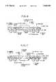
- FIG. 3Ais a cross sectional view showing a semiconductor device in a first preferred embodiment according to the invention.
- FIG. 3Bis an enlarged cross sectional view showing a part of the semiconductor device in FIG. 3A,
- FIGS. 4A to 4Dare cross sectional views showing a method for making the semiconductor device in the first preferred embodiment
- FIG. 5Ais a cross sectional view showing a semiconductor device in a second preferred embodiment according to the invention.
- FIG. 5Bis a cross sectional view showing the mounting state of the semiconductor device in FIG. 5A.
- FIG. 6is a cross sectional view showing a semiconductor device in a third preferred embodiment according to the invention.
- FIG. 7is a cross sectional view showing a semiconductor device in a fourth preferred embodiment according to the invention.
- FIGS. 3A and 3BA semiconductor device in a first preferred embodiment according to the invention will be explained in FIGS. 3A and 3B, wherein like parts are indicated by like reference numerals as used in FIGS. 1A and 1B.
- FIG. 3Ais a cross sectional view showing the semiconductor device in the first preferred embodiment
- FIG. 3Bis an enlarged cross sectional view showing a part of the semiconductor device in FIG. 3A which is indicated by a circle A.
- the semiconductor device in the first embodimentcomprises a semiconductor IC chip 1, a base film 2 forming a basis of a film carrier tape, through-holes 2a and device holes 2b which open in the base film 2, a copper-foil wiring 3 formed on the base film 2, inner leads 3a formed at the inside end of the copper-foil wiring 3, lands 3b for connecting to outside, apertures 3c formed in the center of the respective lands 3b, cover resist 4 formed on the base film 2 except the lands 3b, sealing resin 5 for protecting the semiconductor IC chip 1 and solder bumps 6.
- the dimensions of the opening portions of the through-hole 2a, the aperture 3c in the copper-foil wiring 3 and the cover resist 4are, as shown in FIG. 3B, ⁇ 2, ⁇ 1 and ⁇ 3, respectively, they are formed to keep the relationship of ⁇ 3 ⁇ 2> ⁇ 1.
- the film carrier tapeis made by a method for making a conventional three layers-one metal composition tape.
- the through-holes 2aare opened together with the device holes 2b by a punching or laser method.
- the copper-foil wiring 3which includes the inner leads 3a and land 3b and in which the apertures 3c is formed is formed by resist-coating, exposing, developing and etching to a copper tape.
- the cover resist 4has a predetermined pattern formed by a screen-printing method or the like.
- the solder bumps 6are formed by, for example, disposing solder balls on the lands 3b and re-flowing them.
- the dimensions ( ⁇ 2) of the through-holes 2ais 0.35 to 0.4 mm
- the dimensions (100 1) of the apertures 3c in the copper-foil wiring 3is 0.2 to 0.25 mm
- the dimensions ( ⁇ 3) openings of the cover resist 4is 0.4 to 0.6 mm.
- the height of the solder bump 6becomes about 0.5 to 0.8 mm when a solder ball with a diameter of 0.7 to 0.9 mm is provided and re-flown.
- solderclimbs up to the though-hole 2a through the aperture 3c since the aperture 3c formed in the land 3b gives an escape for the flux and decomposed gas of the solder ball.
- the climbed solder 6adoes not reach the surface of the base film 2 since the side of the through-hole 2a is not plated and the base film 2 is made of polyimide or polyester resin which does not have a good wetness property to the solder. It stops at a constant level from behind the land 3b thereby uniforming the profile and height of the solder bump 6.
- the adhesion strength of the solder bump 6 to the land 3bcan be enhanced since solder is connecting between the front and back surfaces of land 3b through the aperture 3c. Furthermore, since the climbed solder 6a connected to the surface of the base film 2 can be observed from the backside of the base film 2, the junction state of the solder bump 6 can be easily checked.
- FIGS. 4A to 4Dare cross sectional views showing a method for making the semiconductor device in the first embodiment.
- the electrode 1a of the semiconductor IC chip 1is bonded to the inner lead 3a extending from the film carrier tape as explained in FIGS. 3A and 3B.
- the copper-foil wiring 3is formed by a copper foil with a thickness of about 35 ⁇ m.
- the surface of the inner lead 3a or land 3bmay be provided with gold plating with a thickness of 0.2 to 1.0 ⁇ m, or tin plating with a thickness of 0.3 to 0.5 ⁇ m.
- the semiconductor IC chip 1has a bump with a thickness of about 10 to 30 ⁇ m as an electrode 1a.
- an aluminum electrode with a thickness of about 1 to 2 ⁇ mwhich is in general provided with the semiconductor IC chip may be used as it is.
- a package bonding manner (gang bonding manner) or a single point mannercan be employed when the bump is formed as the electrode 1a. If the electrode 1a is an aluminum electrode, the single point manner can be employed.
- the sealing resin 5is formed by supplying resin to the electrode side of the semiconductor IC chip by a potting method and curing it. This is not only for protecting the semiconductor IC chip, but also for protecting the inner lead 3a and securely fixing it to the base film 2.
- the potting methodmay be replaced by a screen printing method or the like.
- the thickness of the sealing resin 5is desirably about 200 to 300 ⁇ m from the surface of the semiconductor IC chip 1.
- the solder bump 6is formed by coating with flux, supplying a solder ball thereto and re-flowing it.
- a screen printing method, a dispenser method, an injection method of supplying fused solder, a ball bonding method of using a solder wire or the likecan be used as the method for forming the solder bump 6, a screen printing method, a dispenser method, an injection method of supplying fused solder, a ball bonding method of using a solder wire or the like can be used.
- the solder bumpmay be replaced by another metal bump.
- a metal ball covered with soldercan be used to form the bump.
- the film carrier BGA type semiconductor device made by such processis mounted on the mounting substrate 9 by means of pads 9a and the solder bumps 6 in a package re-flowing manner.
- solder bumps 6is formed by using solder balls
- mounting to the mounting substrate 9can be performed only by providing solder paste with a thickness of 0.1 to 0.2 mm as the pads 9a and can be performed together with another surface mounting type package, for example, QFP (quad flat package), in the same re-flowing manner.
- QFPquad flat package
- the junction state of the solder to the landcan be easily checked from outside at the stage of supplying the solder balls to the package to form the solder bump 6. Furthermore, also in mounting the BGA package on the mounting substrate 9, the junction state of the solder can be checked by looking at the climbed solder 6a from the through-holes 2a in the base film 2.
- the BGA packagecan be made at a low cost since it uses the film carrier of a cheaper three layers-one metal composition.
- FIG. 5Ais a cross sectional view showing the semiconductor device in the second preferred embodiment
- FIG. 5Bis a cross sectional view showing the state of mounting the semiconductor device in FIG. 5A.
- the semiconductor device in the second embodimentcomprises a semiconductor IC chip 1, a base film 2, through-holes 2a which open in the base film 2, a copper-foil wiring 3, inner leads 3a, land 3b, apertures 3c formed in the center of the respective lands 3b, cover resist 4, sealing resin 5, solder bumps 6 and climbed solder 6a.
- the difference from the first embodimentis that the solder bumps 6 are formed from the copper-foil wiring 3 toward the base film 2.
- the film carrier tapeis also made by a method for making a conventional three layers-one metal composition tape.
- ⁇ 11is 0.1 to 0.2 mm
- ⁇ 22is 0.3 to 0.35 mm
- ⁇ 33is 0.35 to 0.5 mm
- the height of the solder bump 6becomes about 0.4 to 0.6 mm.
- solder ballsdo not short each other since the bump pitch P2 is 1.0 mm and the diameter of the solder ball is 0.6 to 0.7 mm to which ⁇ 22 is 0.3 to 0.35 mm and the base film 2 is made of polyimide resin or the like which does not have a good wetness property to the solder.
- solderclimbs up to the cover resist 4 through the aperture 3c with ⁇ 11 of 0.15 and 0.2 mm formed in the center of the land 3b to form the climbed solder 6a, where the aperture 3c gives an escape for the flux and decomposed gas of the solder ball.
- the climbed bumps 6ado not short each other and the solder bumps 6 after re-flowing have an uniform profile and height of 0.4 to 0.6 mm.
- the junction state of the solder bump 6 which is formed on the back of the base film to land 3bcan be easily checked.
- the semiconductor device made by such processis mounted on the mounting substrate 9 by means of pads 9a and the solder bumps 6 in a package re-flowing manner.
- the back surface of the semiconductor IC chip 1may also be adhered to the mounting substrate 9 by a pad 9b.
- solder bumps 6are formed from the copper-foil wiring 3 toward the base film 2.
- the semiconductor IC chip 1is placed facing to the front surface of the base film 2, i.e., in a face-up manner.
- FIG. 7a semiconductor device in a fourth preferred embodiment will be explained in FIG. 7, wherein like parts are indicated by like reference numerals as used in FIGS. 3A and 3B.
- the semiconductor IC chip 1is placed facing to the back surface of the base film 2, i.e., in a face-down manner.
- a semiconductor IC chipmay be bonded in both a face-up manner and a face-down manner.
- bumpsmay be formed on both a base film and a cover resist. Therefore, the structure of the semiconductor device can be optionally selected depending on the characteristics and mounting structure of an IC chip.
- the semiconductor device according to the inventionhas a structure that the junction state of a solder bump to a copper-foil wiring and the junction state of a package to a mounting substrate can be easily checked. Further, the electrical characteristics of the semiconductor device can be easily observed even after mounting. Thereby, it has an advantage that one can instantly judge the semiconductor device to be repaired or to be again re-flown.
Landscapes
- Engineering & Computer Science (AREA)
- Microelectronics & Electronic Packaging (AREA)
- Computer Hardware Design (AREA)
- Power Engineering (AREA)
- Physics & Mathematics (AREA)
- Condensed Matter Physics & Semiconductors (AREA)
- General Physics & Mathematics (AREA)
- Manufacturing & Machinery (AREA)
- Wire Bonding (AREA)
- Lead Frames For Integrated Circuits (AREA)
Abstract
Description
This invention relates to a semiconductor device, and more particularly to, a semiconductor device in which a semiconductor integrated circuit is mounted on a film carrier tape.
A method for making a conventional semiconductor device with a film carrier tape is as follows:
Prepared is a base film which is made of polyimide, polyester, glass-epoxy or the like and in which sprocket holes for carrying and positioning and device holes for placing semiconductor devices are opened. A metal foil of copper or the like is adhered to the base film by adhesives, thereafter etching the metal foil to form leads with given shapes and pads for electrical selection.
Next, the inner lead bonding (hereinafter referred to as "ILB") of the leads extending in the device hole of the film carrier tape to bumps formed on electrodes of an IC chip is carried out by a thermo-compression method of eutectic method. In the film carrier tape, an electrical selection test and BT (burn-in test) is then conducted. Whereafter, the leads are cut to desirable lengths to carry out outer lead bonding (hereinafter referred to as "OLB").
Herein, in the case of leads with many pins, to prevent the portions for OLB from scattering, a method of leaving insulating film composing the film carrier tape on the outer end of the outer leads is often employed. Thereafter, mounting is carried out, for example, by OLB of the leads to the bonding pads on a printed substrate.
In such method for mounting the semiconductor device with a film carrier tape, when OLB to the printed substrate is carried out, it is difficult to obtain coplanarity in leads for OLB since the lead for OLB is thin to about 35 μm. To deal with this, a bonding tool for OLB which is only used for a film carrier tape was required.
On the other hand, when it is mounted on the same substrate with another package which can be mounted by package re-flowing, for example, QFP (Quad Flat Package), the mounting thereof has to be carried out on the step separated from the re-flowing step. Because of this, a film carrier tape type semiconductor device is exactly used as a special package since it is not multipurpose.
Herein, the outer re-flow pitch in QFP which can be re-flown is limited to about 0.4 mm.
As a surface mounting type package for adapting to the limitation, "Nikkei Microdevices", pp. 58-64, March, 1994 describes BGA (Ball Grid Allay) in which solder bumps as outer terminals are disposed in the form of a lattice on the backside of the package. When a package with 220 pins and a square size of 23 to 24 mm is designed, BGA can realize a pitch of about 1.5 mm, whereas QFP needs a pitch of at least about 0.4 mm. Therefore, BGA is excellent in the mounting performance.
Further, since the outer size of BGA is small, the length of wiring in the package becomes shorter, thereby obtaining a good electrical properties. Though this BGA package uses a multilayer printed substrate, it can employ a ceramic substrate or film carrier tape.
For example, as BGA using a film carrier tape, there is a BGA package (hereinafter referred to as "first prior art") suggested by IBM corporation (EIAJ-JEDEC JWG#2-7 "TAPE BALL GRID ARRAY", May, 1994).
FIG. 1A is a cross sectional view showing the BGA package, and FIG. 1B is a enlarged cross sectional view showing a part of the BGA package which is indicated by a circle B in FIG. 1A.
In the BGA package, a copper-foil wiring 3 formed on abase film 2 is connected to aland 3b formed under the base film and a through-hole plating 3d, i.e., the film carrier tape is composed by so called a two layers-two metal technique. In theland 3b, a solder bump as an outer terminal is formed by providing asolder ball 11. Abump 1b on asemiconductor IC chip 1 is connected to the inner lead 3a of the copper-foil wiring 3. Further, a reinforcing plate 13 is pasted by an adhesive 12 thereon to reinforce the film carrier tape, and aheat spreader 15 is pasted byadhesives semiconductor IC chip 1 and reinforcing plate 13 to reduce the heat resistance.
When the BGA semiconductor device is mounted on the mounting substrate, solder paste is provided with the pads on the mounting substrate, thereafter adhering to thesolder ball 11 to mount it.
However, in the BGA package with a film carrier tape, the cost making thereof increases to about five to ten times as compared with a film carrier tape made by a conventional three layers-one metal technique, since the film carrier tape thereof is made by the two layers-two metal technique.
On the other hand, the film carrier tape made by the two layers-two metal technique is subject to lack of mechanical strength caused by the tape thickness of about 50 to 70 μm, thereby causing an undulation or bend of the substrate to reduce the easiness of mounting which is a excellent property of BGA. Therefore, it needs the reinforcing plate 13 for reinforcing the mechanical strength. However, there is a problem that thesolder ball 11 as a connecting means to the substrate can not be checked with the naked eye after mounting. Though the mounting state can be optionally checked by the other way, for example, a x-ray instrument, it is not a proper way for the mass production and it will result in a package with high cost. In brief, the first prior art lacks in the easiness of mounting and it is not multipurpose to various use.
Next, Japanese Patent Applications Laid-Open No. 61-51945 and 1-258454 disclose another type of semiconductor device in which the state of soldering after mounting can be checked on a package substrate. FIGS. 2A and 2B shows the semiconductor device disclosed in Japanese Patent Applications Laid-Open No. 1-258454 (hereinafter referred to as "second prior art").
The semiconductor device is called LGA (Land Grid Array). It uses a rigid substrate as apackage substrate 16 which is similar to that of the above-mentioned standard BGA package, forming a copper-foil wiring on and under thesubstrate 16, connecting betweenlands hole plating 17c, further compressing and bonding a copper plate to the center of the backside of the substrate.Solder plating 19 is provided with theland 17b.
Asemiconductor IC chip 1 is adhered by an adhesive 10 to the concave portion formed in the center of the substrate. Thesemiconductor IC chip 1 and the copper-foil wiring 17 are connected by abonding wire 20, thereafter being sealed with sealingresin 5.
When the LGA package is mounted on amounting substrate 9, as shown in FIG. 2B, solder paste is previously coated to the pads oneh mounting substrate 9 by a screen printing method or the like, positioning and mounting the LGA package to themounting substrate 9 and re-flowing the solder.
In the mounting, i.e., re-flowing, process, solder 21 on themounting substrate 9 climbs up passing the through-hole to form climbed solder 21a. The solder junction between themounting substrate 9 and thepackage substrate 16 can be checked through the climbedsolder 21.
On the other hand, Japanese Patent Application Laid-Open No. 63-34936 discloses a LGA package with a film carrier tape (hereinafter referred to as "third prior art"). This package is made by forming a copper-foil wiring on the film carrier tape, forming a land on the backside of the tape, connecting them by a through-hole and carrying out ILB of a semiconductor IC chip to the inner leads of the copper-foil wiring. Similarly to the second prior art, this package is mounted after solder paste is previously coated to a mounting substrate.
However, in this package, it is not impossible to check the state of the solder junction from outside after mounting since the copper-foil wiring on the substrate is formed to cover the through-hole.
Accordingly, in the BGA or LGA type semiconductor device, mass producibility, excellent mounting performance, easiness of outside checking after mounting, low package cost and the like are required. Among these requirements, the easiness of outside checking is a most important requirement since it relates to an electrical test, repairing etc. after mounting.
Hereon, the first and third prior arts have a problem that the state of the solder junction can not be observed after mounting. In addition, in the first prior art, the package cost becomes higher since the package employs a film carrier tape of two layers-two metals structure, and the package lacks in mass producibility since it needs the reinforcing plate 13.
In the second prior art, as shown in FIG. 2B, it is possible to check the state of the solder junction from outside after mounting. However, this package lacks in mass producibility in that it uses a rigid substrate as a substrate, as compared with a package using a film carrier tape. Further, in this package structure, the through-hole plating 17c, the solder plating 19 on theland 17b and thecopper plate 18 for maintaining the level even to the soldered portion after mounting are required. Thus, the package structure is complex, and the package cost becomes higher.
In addition, in the second and third prior arts, solder required in mounting is provided not with the package but with the mounting substrate. The solder of solder paste or the like is supplied to a screen printing method. For example, when the pitch P3 between thelands 17b is 1.27 mm, the diameter of the land is to be about 0.5 to 0.6 mm. Herein, the gap between the package and the mounting substrate after mounting needs to be about 0.5 to 1.0 mm in order to securely connect therebetween and reduce a thermal stress occurred therebetween by the difference in their thermal expansion coefficients. Therefore, it is necessary to supply solder paste to have a thickness of 1.0 to 1.5 mm to the land with a diameter of about 0.5 to 0.6 mm. As a result, the package in the second and third prior arts lack in easiness of mounting.
Accordingly, it is an object of the invention to provide a semiconductor device in which the state of the junction of a bump to a land and the state of the junction of a bump to a mounting substrate can be easily checked.
It is another object of the invention to provide a semiconductor device in which electrical characteristics can be easily checked after mounting.
It is a further object of the invention to provide a semiconductor device which satisfies mass producibility and low manufacturing cost.
It is a still further object of the invention to provide a semiconductor device which has an excellent workability in mounting.
According to the invention, a semiconductor device, comprises:
a film carrier tape comprising a base film in which a device hole and a through-hole are formed and a metal-foil wiring layer formed on the base film, wherein the metal-foil wiring layer includes one end extending into the device hole to form a inner lead and the other end extending onto the through-hole to form a land;
a semiconductor integrated circuit chip which is provided with an electrode which is connected with the inner lead of the metal-foil wiring layer;
sealing resin for protecting the semiconductor integrated circuit chip; and
a bump which is formed on the land and is formed on a front or back surface of the base film, the bump being made of a conductive material;
wherein an aperture with dimensions smaller than the through-hole is formed in the center of the land of the metal-foil wiring layer.
The invention will be explained in more detail in conjunction with the appended drawings, wherein:
FIG. 1A is a cross sectional view showing a conventional semiconductor device,
FIG. 1B is an enlarged cross sectional view showing a part of the semiconductor device in FIG. 1A,
FIG. 2A is a cross sectional view showing another conventional semiconductor device,
FIG. 2B is a front view showing the mounting state of the semiconductor device in FIG. 2A,
FIG. 3A is a cross sectional view showing a semiconductor device in a first preferred embodiment according to the invention,
FIG. 3B is an enlarged cross sectional view showing a part of the semiconductor device in FIG. 3A,
FIGS. 4A to 4D are cross sectional views showing a method for making the semiconductor device in the first preferred embodiment,
FIG. 5A is a cross sectional view showing a semiconductor device in a second preferred embodiment according to the invention,
FIG. 5B is a cross sectional view showing the mounting state of the semiconductor device in FIG. 5A,
FIG. 6 is a cross sectional view showing a semiconductor device in a third preferred embodiment according to the invention, and
FIG. 7 is a cross sectional view showing a semiconductor device in a fourth preferred embodiment according to the invention.
A semiconductor device in a first preferred embodiment according to the invention will be explained in FIGS. 3A and 3B, wherein like parts are indicated by like reference numerals as used in FIGS. 1A and 1B. FIG. 3A is a cross sectional view showing the semiconductor device in the first preferred embodiment, and FIG. 3B is an enlarged cross sectional view showing a part of the semiconductor device in FIG. 3A which is indicated by a circle A.
As shown in FIGS. 3A and 3B, the semiconductor device in the first embodiment comprises asemiconductor IC chip 1, abase film 2 forming a basis of a film carrier tape, through-holes 2a anddevice holes 2b which open in thebase film 2, a copper-foil wiring 3 formed on thebase film 2, inner leads 3a formed at the inside end of the copper-foil wiring 3, lands 3b for connecting to outside,apertures 3c formed in the center of therespective lands 3b, cover resist 4 formed on thebase film 2 except thelands 3b, sealingresin 5 for protecting thesemiconductor IC chip 1 and solder bumps 6.
Herein, when the dimensions of the opening portions of the through-hole 2a, theaperture 3c in the copper-foil wiring 3 and the cover resist 4 are, as shown in FIG. 3B, Φ2, Φ1 and Φ3, respectively, they are formed to keep the relationship of Φ3≧Φ2>Φ1.
The film carrier tape is made by a method for making a conventional three layers-one metal composition tape. The through-holes 2a are opened together with the device holes 2b by a punching or laser method. The copper-foil wiring 3 which includes the inner leads 3a andland 3b and in which theapertures 3c is formed is formed by resist-coating, exposing, developing and etching to a copper tape. The cover resist 4 has a predetermined pattern formed by a screen-printing method or the like. The solder bumps 6 are formed by, for example, disposing solder balls on thelands 3b and re-flowing them.
Herein, for example, to provide the solder bumps 6 with a pitch P1 therebetween of 1.27 mm, the dimensions (Φ2) of the through-holes 2a is 0.35 to 0.4 mm, the dimensions (100 1) of theapertures 3c in the copper-foil wiring 3 is 0.2 to 0.25 mm and the dimensions (Φ3) openings of the cover resist 4 is 0.4 to 0.6 mm. In this case, the height of thesolder bump 6 becomes about 0.5 to 0.8 mm when a solder ball with a diameter of 0.7 to 0.9 mm is provided and re-flown.
In the re-flowing process, solder climbs up to the though-hole 2a through theaperture 3c since theaperture 3c formed in theland 3b gives an escape for the flux and decomposed gas of the solder ball. The climbed solder 6a does not reach the surface of thebase film 2 since the side of the through-hole 2a is not plated and thebase film 2 is made of polyimide or polyester resin which does not have a good wetness property to the solder. It stops at a constant level from behind theland 3b thereby uniforming the profile and height of thesolder bump 6.
Hereon, the adhesion strength of thesolder bump 6 to theland 3b can be enhanced since solder is connecting between the front and back surfaces ofland 3b through theaperture 3c. Furthermore, since the climbed solder 6a connected to the surface of thebase film 2 can be observed from the backside of thebase film 2, the junction state of thesolder bump 6 can be easily checked.
FIGS. 4A to 4D are cross sectional views showing a method for making the semiconductor device in the first embodiment. At first, as shown in FIG. 4A, theelectrode 1a of thesemiconductor IC chip 1 is bonded to the inner lead 3a extending from the film carrier tape as explained in FIGS. 3A and 3B. Herein, the copper-foil wiring 3 is formed by a copper foil with a thickness of about 35 μm. Optionally, the surface of the inner lead 3a orland 3b may be provided with gold plating with a thickness of 0.2 to 1.0 μm, or tin plating with a thickness of 0.3 to 0.5 μm.
Thesemiconductor IC chip 1 has a bump with a thickness of about 10 to 30 μm as anelectrode 1a. However, an aluminum electrode with a thickness of about 1 to 2 μm which is in general provided with the semiconductor IC chip may be used as it is. In the method for bonding the inner lead, a package bonding manner (gang bonding manner) or a single point manner can be employed when the bump is formed as theelectrode 1a. If theelectrode 1a is an aluminum electrode, the single point manner can be employed.
Next, as shown in FIG. 4B, the sealingresin 5 is formed by supplying resin to the electrode side of the semiconductor IC chip by a potting method and curing it. This is not only for protecting the semiconductor IC chip, but also for protecting the inner lead 3a and securely fixing it to thebase film 2. For supplying the resin, the potting method may be replaced by a screen printing method or the like. The thickness of the sealingresin 5 is desirably about 200 to 300 μm from the surface of thesemiconductor IC chip 1.
Thereafter, as shown in FIG. 4C, thesolder bump 6 is formed by coating with flux, supplying a solder ball thereto and re-flowing it. As the method for forming thesolder bump 6, a screen printing method, a dispenser method, an injection method of supplying fused solder, a ball bonding method of using a solder wire or the like can be used. The solder bump may be replaced by another metal bump. For example, a metal ball covered with solder can be used to form the bump.
The film carrier BGA type semiconductor device made by such process, as shown in FIG. 4D, is mounted on the mountingsubstrate 9 by means ofpads 9a and the solder bumps 6 in a package re-flowing manner.
In the semiconductor device, since the solder bumps 6 is formed by using solder balls, mounting to the mountingsubstrate 9 can be performed only by providing solder paste with a thickness of 0.1 to 0.2 mm as thepads 9a and can be performed together with another surface mounting type package, for example, QFP (quad flat package), in the same re-flowing manner.
As explained above, in the film carrier BGA type semiconductor device in the first embodiment, since theaperture 3c is formed in the center of theland 3b and the through-hole 2a is formed in thebase film 2, the junction state of the solder to the land can be easily checked from outside at the stage of supplying the solder balls to the package to form thesolder bump 6. Furthermore, also in mounting the BGA package on the mountingsubstrate 9, the junction state of the solder can be checked by looking at the climbed solder 6a from the through-holes 2a in thebase film 2.
Thus, the BGA package can be made at a low cost since it uses the film carrier of a cheaper three layers-one metal composition.
With reference to FIGS. 5A and 5B, a semiconductor device in a second preferred embodiment will be explained. Herein, FIG. 5A is a cross sectional view showing the semiconductor device in the second preferred embodiment, and FIG. 5B is a cross sectional view showing the state of mounting the semiconductor device in FIG. 5A.
As shown in FIG. 5A, the semiconductor device in the second embodiment comprises asemiconductor IC chip 1, abase film 2, through-holes 2a which open in thebase film 2, a copper-foil wiring 3, inner leads 3a,land 3b,apertures 3c formed in the center of therespective lands 3b, cover resist 4, sealingresin 5, solder bumps 6 and climbed solder 6a. The difference from the first embodiment is that the solder bumps 6 are formed from the copper-foil wiring 3 toward thebase film 2.
Herein, when the dimensions of the opening portions of the through-hole 2a, theaperture 3c in the copper-foil wiring 3 and the cover resist 4 are, as shown in FIG. 5A, Φ22, Φ11 and Φ33, respectively, they are formed to keep the relationship of Φ33≧Φ22>Φ11. The film carrier tape is also made by a method for making a conventional three layers-one metal composition tape.
Herein, for example, to provide the solder bumps 6 with a pitch P2 therebetween of 1.0 mm, Φ11 is 0.1 to 0.2 mm, Φ22 is 0.3 to 0.35 mm and Φ33 is 0.35 to 0.5 mm, thereafter coating the through-hole 2a with flux, supplying a solder ball with a diameter of 0.6 to 0.7 mm and re-flowing it. In this case, the height of thesolder bump 6 becomes about 0.4 to 0.6 mm.
In this re-flowing process, the solder balls do not short each other since the bump pitch P2 is 1.0 mm and the diameter of the solder ball is 0.6 to 0.7 mm to which Φ22 is 0.3 to 0.35 mm and thebase film 2 is made of polyimide resin or the like which does not have a good wetness property to the solder. On the other hand, solder climbs up to the cover resist 4 through theaperture 3c with Φ11 of 0.15 and 0.2 mm formed in the center of theland 3b to form the climbed solder 6a, where theaperture 3c gives an escape for the flux and decomposed gas of the solder ball.
Since the backside of theland 3b is coated with the cover resist 4 which does not have a good wetness property, the climbed bumps 6a do not short each other and the solder bumps 6 after re-flowing have an uniform profile and height of 0.4 to 0.6 mm.
In this embodiment, since the climbed solder 6a can be observed from the front of thebase film 2, the junction state of thesolder bump 6 which is formed on the back of the base film toland 3b can be easily checked.
The semiconductor device made by such process, as shown in FIG. 5B, is mounted on the mountingsubstrate 9 by means ofpads 9a and the solder bumps 6 in a package re-flowing manner. Herein, the back surface of thesemiconductor IC chip 1 may also be adhered to the mountingsubstrate 9 by apad 9b. Thereby, according to this embodiment, even if the semiconductor IC chip generates much heat, heat can be discharged from the chip to the mountingsubstrate 9.
Next, a semiconductor device in a third preferred embodiment will be explained in FIG. 6, wherein like parts are indicated by like reference numerals as used in FIGS. 5A and 5B. Also in the third embodiment, the solder bumps 6 are formed from the copper-foil wiring 3 toward thebase film 2. However, thesemiconductor IC chip 1 is placed facing to the front surface of thebase film 2, i.e., in a face-up manner.
Further, a semiconductor device in a fourth preferred embodiment will be explained in FIG. 7, wherein like parts are indicated by like reference numerals as used in FIGS. 3A and 3B. In the fourth embodiment, thesemiconductor IC chip 1 is placed facing to the back surface of thebase film 2, i.e., in a face-down manner.
Thus, in the film carrier BGA type semiconductor device according to the invention, a semiconductor IC chip may be bonded in both a face-up manner and a face-down manner. Also, bumps may be formed on both a base film and a cover resist. Therefore, the structure of the semiconductor device can be optionally selected depending on the characteristics and mounting structure of an IC chip.
The semiconductor device according to the invention has a structure that the junction state of a solder bump to a copper-foil wiring and the junction state of a package to a mounting substrate can be easily checked. Further, the electrical characteristics of the semiconductor device can be easily observed even after mounting. Thereby, it has an advantage that one can instantly judge the semiconductor device to be repaired or to be again re-flown.
Though the invention has been described with respect to specific embodiment for complete and clear disclosure, the appended claims are not to be thus limited but are to be construed as embodying all modification and alternative constructions that may be occurred to one skilled in the art which fairly fall within the basic teaching here is set forth.
Claims (8)
1. A semiconductor device, comprising:
a film carrier tape comprising a base film in which a device hole and through-hole are formed and a metal-foil wiring layer formed on said base film, wherein said metal-foil writing layer includes one coplanar end extending into said device hole to form an inner lead and the other coplanar end extending onto said through-hole to form a land;
a semiconductor integrated circuit chip which is provided with an electrode which is connected with said inner lead of said metal-foil wiring layer;
sealing resin for protecting said semiconductor integrated circuit chip; and
a bump which is formed on said land and is formed on a front or back surface of said base film, said bump being made of a conductor material;
wherein an aperture with dimensions smaller than said through-hole is formed in the center of said land of said metal-foil wiring layer, whereby the material of the bump contacts both the front and back surfaces of the land.
2. A semiconductor device, according to claim 1, further comprising:
cover resist which is formed on said metal-foil wiring layer and has an opening corresponding to said land.
3. A semiconductor device, according to claim 2, wherein:
said opening of said cover resist has dimensions bigger than said through-hole.
4. A semiconductor device, according to claim 1, wherein:
said bump is made of a solder ball.
5. A semiconductor device, according to claim 1, wherein:
said bump has a portion which climbs up through said aperture onto a surface reverse to the surface where said bump is formed.
6. A semiconductor device, according to claim 1, wherein:
said inner lead and/or said land of said metal-foil layer is plated by gold or tin.
7. A semiconductor device, according to claim 1, wherein:
said electrode of said semiconductor integrated circuit forms a bump.
8. A semiconductor device, comprising:
a film carrier tape comprising a base film in which a device hole and a through-hole are formed and a metal-foil wiring layer formed on said base film, wherein said metal-foil wiring layer includes one end extending into said device hole to form an inner lead and the other end extending onto said through-hole to form a land having front and back surfaces;
a semiconductor integrated circuit chip which is provided with an electrode which is connected with said inner lead of said metal-foil wiring layer;
a bump which is formed on said land and is formed on a front or back surface of said base film, said bump being made of a conductive material;
the land in the region of the through-hole having a dimension smaller than said through-hole whereby the material of the bump contacts both the front and back surfaces of the land.
Applications Claiming Priority (2)
| Application Number | Priority Date | Filing Date | Title |
|---|---|---|---|
| JP6244922AJP2595909B2 (en) | 1994-09-14 | 1994-09-14 | Semiconductor device |
| JP6-244922 | 1994-09-14 |
Publications (1)
| Publication Number | Publication Date |
|---|---|
| US5668405Atrue US5668405A (en) | 1997-09-16 |
Family
ID=17125976
Family Applications (1)
| Application Number | Title | Priority Date | Filing Date |
|---|---|---|---|
| US08/528,244Expired - Fee RelatedUS5668405A (en) | 1994-09-14 | 1995-09-14 | Semiconductor device with a film carrier tape |
Country Status (4)
| Country | Link |
|---|---|
| US (1) | US5668405A (en) |
| EP (1) | EP0702404B1 (en) |
| JP (1) | JP2595909B2 (en) |
| DE (1) | DE69525697T2 (en) |
Cited By (119)
| Publication number | Priority date | Publication date | Assignee | Title |
|---|---|---|---|---|
| US5837558A (en)* | 1997-11-04 | 1998-11-17 | Texas Instruments Incorporated | Integrated circuit chip packaging method |
| US5847455A (en)* | 1995-11-07 | 1998-12-08 | Vlsi Technology, Inc. | Molded leadframe ball grid array |
| US5863812A (en)* | 1996-09-19 | 1999-01-26 | Vlsi Technology, Inc. | Process for manufacturing a multi layer bumped semiconductor device |
| US5872405A (en)* | 1996-05-28 | 1999-02-16 | Micron Technology, Inc. | Laser wire bonding for wire embedded dielectrics to integrated circuits |
| US5872399A (en)* | 1996-04-01 | 1999-02-16 | Anam Semiconductor, Inc. | Solder ball land metal structure of ball grid semiconductor package |
| US5892271A (en)* | 1995-04-18 | 1999-04-06 | Nec Corporation | Semiconductor device |
| US5894107A (en)* | 1996-08-19 | 1999-04-13 | Samsung Electronics Co., Ltd. | Chip-size package (CSP) using a multi-layer laminated lead frame |
| US5910686A (en)* | 1998-07-23 | 1999-06-08 | Vlsi Technology, Inc. | Cavity down HBGA package structure |
| US5969424A (en)* | 1997-03-19 | 1999-10-19 | Fujitsu Limited | Semiconductor device with pad structure |
| US5977633A (en)* | 1996-08-15 | 1999-11-02 | Nec Corporation | Semiconductor device with metal base substrate having hollows |
| US5982026A (en)* | 1996-07-16 | 1999-11-09 | Nec Corporation | Inexpensive resin molded semiconductor device |
| US5982033A (en)* | 1995-09-20 | 1999-11-09 | Sony Corporation | Semiconductor chip package |
| US6013953A (en)* | 1997-01-16 | 2000-01-11 | Nec Corporation | Semiconductor device with improved connection reliability |
| US6023097A (en)* | 1999-03-17 | 2000-02-08 | Chipmos Technologies, Inc. | Stacked multiple-chip module micro ball grid array packaging |
| US6028358A (en)* | 1996-05-30 | 2000-02-22 | Nec Corporation | Package for a semiconductor device and a semiconductor device |
| US6057594A (en)* | 1997-04-23 | 2000-05-02 | Lsi Logic Corporation | High power dissipating tape ball grid array package |
| US6072233A (en)* | 1998-05-04 | 2000-06-06 | Micron Technology, Inc. | Stackable ball grid array package |
| US6084300A (en)* | 1997-04-21 | 2000-07-04 | Oki Electric Industry Co., Ltd. | Compact resin-sealed semiconductor device |
| US6104091A (en)* | 1996-05-24 | 2000-08-15 | Sony Corporation | Semiconductor package and the manufacturing method |
| US6111324A (en)* | 1998-02-05 | 2000-08-29 | Asat, Limited | Integrated carrier ring/stiffener and method for manufacturing a flexible integrated circuit package |
| US6114753A (en)* | 1996-05-30 | 2000-09-05 | Hitachi, Ltd. | Circuit tape having adhesive film, semiconductor device, and a method for manufacturing the same |
| US6118178A (en)* | 1998-01-09 | 2000-09-12 | Sony Corporation | Circuit film utilizing a power supply and ground connections |
| US6121576A (en)* | 1998-09-02 | 2000-09-19 | Micron Technology, Inc. | Method and process of contact to a heat softened solder ball array |
| US6159837A (en)* | 1998-07-16 | 2000-12-12 | Kabushiki Kaisha Toshiba | Manufacturing method of semiconductor device |
| US6229222B1 (en)* | 1998-06-09 | 2001-05-08 | Oki Electric Industry Co., Ltd. | Semiconductor device and method of fabricating the same |
| WO2001037337A1 (en)* | 1999-11-15 | 2001-05-25 | Substrate Technologies, Inc. | Ball grid substrate for lead-on-chip semiconductor package |
| US6281571B1 (en)* | 1999-03-26 | 2001-08-28 | Fujitsu Limited | Semiconductor device having an external connection electrode extending through a through hole formed in a substrate |
| US6282062B1 (en)* | 1998-02-27 | 2001-08-28 | Tdk Corporation | Magnetic head apparatus with head IC chip |
| US20010041381A1 (en)* | 2000-05-10 | 2001-11-15 | Samsung Electronics, Co., Ltd | Method for manufacturing digital micro-mirror device (DMD) packages |
| US6323551B1 (en)* | 1997-10-27 | 2001-11-27 | Oki Electric Industry Co., Ltd. | Resin sealed-type semiconductor device and method of manufacturing the same |
| US6365439B2 (en)* | 1996-03-22 | 2002-04-02 | Hitachi, Ltd. | Method of manufacturing a ball grid array type semiconductor package |
| US6365980B1 (en)* | 1999-02-26 | 2002-04-02 | Texas Instruments Incorporated | Thermally enhanced semiconductor ball grid array device and method of fabrication |
| US20020043397A1 (en)* | 2000-07-31 | 2002-04-18 | Tongbi Jiang | Method of selectively adjusting surface tension of soldermask material |
| US6404067B1 (en) | 1998-06-01 | 2002-06-11 | Intel Corporation | Plastic ball grid array package with improved moisture resistance |
| SG89283A1 (en)* | 1998-07-14 | 2002-06-18 | Nat Starch Chem Invest | Method of preparing an electronic package by co-curing adhesive and encapsulant |
| US6420664B1 (en)* | 1998-11-26 | 2002-07-16 | Shinko Electric Industries, Co., Ltd. | Metal foil having bumps, circuit substrate having the metal foil, and semiconductor device having the circuit substrate |
| US6420789B1 (en) | 2000-05-16 | 2002-07-16 | Micron Technology, Inc. | Ball grid array chip packages having improved testing and stacking characteristics |
| US6424036B1 (en)* | 1998-09-17 | 2002-07-23 | Nec Corporation | Semiconductor device and method for manufacturing the same |
| US6423576B1 (en) | 1997-10-14 | 2002-07-23 | Amkor Technology, Inc. | Microelectronic device package having a heat sink structure for increasing the thermal conductivity of the package |
| US6433440B1 (en) | 1997-06-06 | 2002-08-13 | Hitachi, Ltd. | Semiconductor device having a porous buffer layer for semiconductor device |
| US6448506B1 (en) | 2000-12-28 | 2002-09-10 | Amkor Technology, Inc. | Semiconductor package and circuit board for making the package |
| US6455354B1 (en) | 1998-12-30 | 2002-09-24 | Micron Technology, Inc. | Method of fabricating tape attachment chip-on-board assemblies |
| US20020164838A1 (en)* | 2001-05-02 | 2002-11-07 | Moon Ow Chee | Flexible ball grid array chip scale packages and methods of fabrication |
| US6504245B1 (en)* | 2000-05-24 | 2003-01-07 | Oki Electric Industry Co, Ltd. | Semiconductor device |
| US6512288B1 (en) | 1999-06-07 | 2003-01-28 | Amkor Technology, Inc. | Circuit board semiconductor package |
| US6515356B1 (en) | 1999-05-07 | 2003-02-04 | Amkor Technology, Inc. | Semiconductor package and method for fabricating the same |
| US6541848B2 (en)* | 1998-02-25 | 2003-04-01 | Fujitsu Limited | Semiconductor device including stud bumps as external connection terminals |
| US6552436B2 (en)* | 2000-12-08 | 2003-04-22 | Motorola, Inc. | Semiconductor device having a ball grid array and method therefor |
| US6564454B1 (en) | 2000-12-28 | 2003-05-20 | Amkor Technology, Inc. | Method of making and stacking a semiconductor package |
| US20030098470A1 (en)* | 2000-02-24 | 2003-05-29 | Williams Vernon M. | Stereolithographically fabricated conductive elements, semiconductor device components and assemblies including such conductive elements, and methods |
| US20030136814A1 (en)* | 2002-01-18 | 2003-07-24 | International Business Machines Corporation | High density raised stud microjoining system and methods of fabricating the same |
| US20030141596A1 (en)* | 2000-02-28 | 2003-07-31 | Hidehiro Nakamura | Wiring board, semiconductor device, and method of manufacturing wiring board |
| US20030164543A1 (en)* | 2002-03-04 | 2003-09-04 | Teck Kheng Lee | Interposer configured to reduce the profiles of semiconductor device assemblies and packages including the same and methods |
| US20030164548A1 (en)* | 2002-03-04 | 2003-09-04 | Lee Teck Kheng | Flip chip packaging using recessed interposer terminals |
| US6673651B2 (en)* | 1999-07-01 | 2004-01-06 | Oki Electric Industry Co., Ltd. | Method of manufacturing semiconductor device including semiconductor elements mounted on base plate |
| US20040007771A1 (en)* | 1999-08-24 | 2004-01-15 | Amkor Technology, Inc. | Semiconductor package and method for fabricating the smae |
| US6708871B2 (en)* | 2002-01-08 | 2004-03-23 | International Business Machines Corporation | Method for forming solder connections on a circuitized substrate |
| US20040061220A1 (en)* | 1996-03-22 | 2004-04-01 | Chuichi Miyazaki | Semiconductor device and manufacturing method thereof |
| US6730536B1 (en) | 2001-06-28 | 2004-05-04 | Amkor Technology, Inc. | Pre-drilled image sensor package fabrication method |
| US20040099938A1 (en)* | 2002-09-11 | 2004-05-27 | Tessera, Inc. | Assemblies having stacked semiconductor chips and methods of making same |
| US20040104470A1 (en)* | 2002-08-16 | 2004-06-03 | Tessera, Inc. | Microelectronic packages with self-aligning features |
| US20040113271A1 (en)* | 2001-05-16 | 2004-06-17 | Yoshikazu Takahashi | Tape carrier package having stacked semiconductor elements, and short and long leads |
| US6756251B2 (en) | 2001-08-21 | 2004-06-29 | Micron Technology, Inc. | Method of manufacturing microelectronic devices, including methods of underfilling microelectronic components through an underfill aperture |
| US6774467B2 (en)* | 2000-03-24 | 2004-08-10 | Shinko Electric Industries Co., Ltd | Semiconductor device and process of production of same |
| US20040159957A1 (en)* | 2002-03-04 | 2004-08-19 | Lee Teck Kheng | Interposer substrate and wafer scale interposer substrate member for use with flip-chip configured semiconductor dice |
| US6791194B1 (en) | 1996-05-30 | 2004-09-14 | Hitachi, Ltd. | Circuit tape having adhesive film, semiconductor device, and a method for manufacturing the same |
| US20040203190A1 (en)* | 2001-10-09 | 2004-10-14 | Tessera, Inc. | Stacked packages |
| US20040219713A1 (en)* | 2002-01-09 | 2004-11-04 | Micron Technology, Inc. | Elimination of RDL using tape base flip chip on flex for die stacking |
| US20040217461A1 (en)* | 2002-08-05 | 2004-11-04 | Tessera, Inc. | Microelectronic adaptors, assemblies and methods |
| US20040262777A1 (en)* | 2002-10-11 | 2004-12-30 | Tessera, Inc. | Components, methods and assemblies for multi-chip packages |
| US6838768B2 (en) | 1998-06-30 | 2005-01-04 | Micron Technology Inc | Module assembly for stacked BGA packages |
| US6900580B2 (en)* | 1998-11-12 | 2005-05-31 | The Board Of Trustees Of The Leland Stanford Junior University | Self-oriented bundles of carbon nanotubes and method of making same |
| US6936922B1 (en) | 2003-09-26 | 2005-08-30 | Amkor Technology, Inc. | Semiconductor package structure reducing warpage and manufacturing method thereof |
| US20050196902A1 (en)* | 2004-03-02 | 2005-09-08 | Hu Dyi-Chung | Method of fabricating film carrier |
| US20050263860A1 (en)* | 2004-05-26 | 2005-12-01 | Matsushita Electric Industrial Co., Ltd. | Semiconductor device and method for manufacturing the same |
| US6977440B2 (en) | 2001-10-09 | 2005-12-20 | Tessera, Inc. | Stacked packages |
| US7009296B1 (en) | 2004-01-15 | 2006-03-07 | Amkor Technology, Inc. | Semiconductor package with substrate coupled to a peripheral side surface of a semiconductor die |
| US20060087011A1 (en)* | 2004-10-21 | 2006-04-27 | Nitto Denko Corporation | Wired circuit board |
| US7061120B2 (en) | 1999-05-20 | 2006-06-13 | Amkor Technology, Inc. | Stackable semiconductor package having semiconductor chip within central through hole of substrate |
| US20060128060A1 (en)* | 2001-03-26 | 2006-06-15 | Yoichiro Kurita | Thin planar semiconductor device having electrodes on both surfaces and method of fabricating same |
| US7087460B2 (en) | 2002-03-04 | 2006-08-08 | Micron Technology, Inc. | Methods for assembly and packaging of flip chip configured dice with interposer |
| US7094676B1 (en) | 2000-10-13 | 2006-08-22 | Bridge Semiconductor Corporation | Semiconductor chip assembly with embedded metal pillar |
| US7112520B2 (en) | 2002-03-04 | 2006-09-26 | Micron Technology, Inc. | Semiconductor die packages with recessed interconnecting structures and methods for assembling the same |
| US20070013043A1 (en)* | 2005-07-14 | 2007-01-18 | Yu-Tang Pan | Chip package without core and stacked chip package structure thereof |
| US20070040261A1 (en)* | 2004-02-23 | 2007-02-22 | Wolfgang Hetzel | Semiconductor component comprising an interposer substrate and method for the production thereof |
| US20070052081A1 (en)* | 2005-09-01 | 2007-03-08 | Gerber Mark A | Package-on-package semiconductor assembly |
| US7190080B1 (en)* | 2000-10-13 | 2007-03-13 | Bridge Semiconductor Corporation | Semiconductor chip assembly with embedded metal pillar |
| US20070063331A1 (en)* | 2005-09-16 | 2007-03-22 | Stats Chippac Ltd. | Integrated circuit package system with planar interconnects |
| US20070145548A1 (en)* | 2003-12-22 | 2007-06-28 | Amkor Technology, Inc. | Stack-type semiconductor package and manufacturing method thereof |
| US20070158837A1 (en)* | 2005-07-10 | 2007-07-12 | Nec Electronics Corporation | Semiconductor device |
| US20070216033A1 (en)* | 2006-03-20 | 2007-09-20 | Corisis David J | Carrierless chip package for integrated circuit devices, and methods of making same |
| US7320933B2 (en) | 2002-08-20 | 2008-01-22 | Micron Technology, Inc. | Double bumping of flexible substrate for first and second level interconnects |
| US7329945B2 (en) | 1995-12-19 | 2008-02-12 | Micron Technology, Inc. | Flip-chip adaptor package for bare die |
| US20080042274A1 (en)* | 2002-09-06 | 2008-02-21 | Tessera, Inc. | Components, methods and assemblies for stacked packages |
| US20080042252A1 (en)* | 1998-06-30 | 2008-02-21 | Micron Technology, Inc. | Stackable ceramic fbga for high thermal applications |
| US7335995B2 (en) | 2001-10-09 | 2008-02-26 | Tessera, Inc. | Microelectronic assembly having array including passive elements and interconnects |
| USRE40112E1 (en) | 1999-05-20 | 2008-02-26 | Amkor Technology, Inc. | Semiconductor package and method for fabricating the same |
| US20080251894A1 (en)* | 2006-02-21 | 2008-10-16 | Matsushita Electric Industrial Co., Ltd. | Mounted Body and Method for Manufacturing the Same |
| CN100440469C (en)* | 2005-08-31 | 2008-12-03 | 钰桥半导体股份有限公司 | Method for manufacturing semiconductor chip packaging structure with metal wall at welding end |
| US7545029B2 (en) | 2006-08-18 | 2009-06-09 | Tessera, Inc. | Stack microelectronic assemblies |
| US20090146287A1 (en)* | 1996-12-03 | 2009-06-11 | Oki Electric Industry Co., Ltd. | Semiconductor device having a chip-size package |
| US20090243082A1 (en)* | 2008-03-26 | 2009-10-01 | Zigmund Ramirez Camacho | Integrated circuit package system with planar interconnect |
| US20100046186A1 (en)* | 2008-08-25 | 2010-02-25 | Imbera Electronics Oy | Circuit board structure comprising an electrical component and a method for manufacturing a circuit board structure comprising an electrical component |
| US20100052131A1 (en)* | 2008-08-26 | 2010-03-04 | Lionel Chien Hui Tay | Integrated circuit package system with redistribution layer |
| US20110062577A1 (en)* | 2009-09-16 | 2011-03-17 | Ching-Wei Hung | Substrate and package with micro bga configuration |
| US7915718B2 (en) | 2002-03-04 | 2011-03-29 | Micron Technology, Inc. | Apparatus for flip-chip packaging providing testing capability |
| US20110147059A1 (en)* | 2009-12-17 | 2011-06-23 | Qing Ma | Substrate for integrated circuit devices including multi-layer glass core and methods of making the same |
| US20110156237A1 (en)* | 2009-12-29 | 2011-06-30 | Nxp B.V. | Fan-out chip scale package |
| US8072082B2 (en) | 2008-04-24 | 2011-12-06 | Micron Technology, Inc. | Pre-encapsulated cavity interposer |
| USRE43112E1 (en) | 1998-05-04 | 2012-01-17 | Round Rock Research, Llc | Stackable ball grid array package |
| US20120138968A1 (en)* | 2010-12-07 | 2012-06-07 | Na-Rae Shin | Semiconductor package and display panel assembly having the same |
| US20140085846A1 (en)* | 2012-09-24 | 2014-03-27 | Qing Ma | Microelectronic structures having laminated or embedded glass routing structures for high density packaging |
| US20150049443A1 (en)* | 2013-08-13 | 2015-02-19 | Infineon Technologies Ag | Chip arrangement |
| USRE45463E1 (en) | 2003-11-12 | 2015-04-14 | Tessera, Inc. | Stacked microelectronic assemblies with central contacts |
| CN104681529A (en)* | 2013-11-27 | 2015-06-03 | 英飞凌科技股份有限公司 | Semiconductor package and method for producing the same |
| US9445496B2 (en) | 2012-03-07 | 2016-09-13 | Intel Corporation | Glass clad microelectronic substrate |
| US9466545B1 (en) | 2007-02-21 | 2016-10-11 | Amkor Technology, Inc. | Semiconductor package in package |
| US9686861B2 (en) | 2009-12-17 | 2017-06-20 | Intel Corporation | Glass core substrate for integrated circuit devices and methods of making the same |
| TWI855505B (en)* | 2022-11-14 | 2024-09-11 | 南亞科技股份有限公司 | Semiconductor package and manufacturing method thereof |
Families Citing this family (21)
| Publication number | Priority date | Publication date | Assignee | Title |
|---|---|---|---|---|
| JP2899540B2 (en)* | 1995-06-12 | 1999-06-02 | 日東電工株式会社 | Film carrier and semiconductor device using the same |
| US5783866A (en)* | 1996-05-17 | 1998-07-21 | National Semiconductor Corporation | Low cost ball grid array device and method of manufacture thereof |
| DE19758547B4 (en)* | 1996-05-17 | 2005-01-20 | National Semiconductor Corp.(N.D.Ges.D.Staates Delaware), Santa Clara | Ball grid array for semiconductor component - has substrate plate dimensions forming multiple of dimensions of individual substrate parts |
| DE19719983C2 (en)* | 1996-05-17 | 2003-05-15 | Nat Semiconductor Corp | Mounting plate for semiconductor devices and method for the production thereof |
| US6222272B1 (en) | 1996-08-06 | 2001-04-24 | Nitto Denko Corporation | Film carrier and semiconductor device using same |
| US6093971A (en)* | 1996-10-14 | 2000-07-25 | Fraunhofer-Gesellschaft Zur Forderung Der Angewandten Forschung E.V. | Chip module with conductor paths on the chip bonding side of a chip carrier |
| WO1998022980A1 (en)* | 1996-11-21 | 1998-05-28 | Hitachi, Ltd. | Semiconductor device and process for manufacturing the same |
| KR19980044250A (en)* | 1996-12-06 | 1998-09-05 | 황인길 | Manufacturing Method of Lead Frame and Chip Scale Semiconductor Package Using the Same |
| JP2924840B2 (en)* | 1997-02-13 | 1999-07-26 | 日本電気株式会社 | Tape-BGA type semiconductor device |
| JPH1154658A (en) | 1997-07-30 | 1999-02-26 | Hitachi Ltd | Semiconductor device, method of manufacturing the same, and frame structure |
| JP3645701B2 (en)* | 1997-12-16 | 2005-05-11 | 株式会社三井ハイテック | Semiconductor device |
| JPH11214435A (en)* | 1998-01-26 | 1999-08-06 | Sharp Corp | Semiconductor device and manufacturing method thereof |
| US6400018B2 (en)* | 1998-08-27 | 2002-06-04 | 3M Innovative Properties Company | Via plug adapter |
| DE19907168C1 (en) | 1999-02-19 | 2000-08-10 | Micronas Intermetall Gmbh | Layer arrangement and method for its production |
| US6462414B1 (en) | 1999-03-05 | 2002-10-08 | Altera Corporation | Integrated circuit package utilizing a conductive structure for interlocking a conductive ball to a ball pad |
| DE10126655A1 (en) | 2001-06-01 | 2002-12-05 | Endress & Hauser Gmbh & Co Kg | Circuit board for electronic equipment, has electronic component on first surface with first and second contact surfaces connected by solder or adhesive to first and second contact points with access to track |
| US7205178B2 (en)* | 2004-03-24 | 2007-04-17 | Freescale Semiconductor, Inc. | Land grid array packaged device and method of forming same |
| US7446399B1 (en) | 2004-08-04 | 2008-11-04 | Altera Corporation | Pad structures to improve board-level reliability of solder-on-pad BGA structures |
| JP4842574B2 (en)* | 2005-07-13 | 2011-12-21 | 三菱電機株式会社 | Manufacturing method of semiconductor device |
| US7416923B2 (en)* | 2005-12-09 | 2008-08-26 | International Business Machines Corporation | Underfill film having thermally conductive sheet |
| CN104701191A (en)* | 2013-12-06 | 2015-06-10 | 毅宝力科技有限公司 | Systems and methods for producing manufacturing vectors |
Citations (3)
| Publication number | Priority date | Publication date | Assignee | Title |
|---|---|---|---|---|
| US5397921A (en)* | 1993-09-03 | 1995-03-14 | Advanced Semiconductor Assembly Technology | Tab grid array |
| US5468681A (en)* | 1989-08-28 | 1995-11-21 | Lsi Logic Corporation | Process for interconnecting conductive substrates using an interposer having conductive plastic filled vias |
| US5519936A (en)* | 1994-01-28 | 1996-05-28 | International Business Machines Corporation | Method of making an electronic package with a thermally conductive support member having a thin circuitized substrate and semiconductor device bonded thereto |
Family Cites Families (4)
| Publication number | Priority date | Publication date | Assignee | Title |
|---|---|---|---|---|
| JPS6057222B2 (en)* | 1980-03-26 | 1985-12-13 | シャープ株式会社 | Film carrier type semiconductor device |
| US5045914A (en)* | 1989-12-26 | 1991-09-03 | Motorola, Inc. | Plastic pad array electronic AC device |
| US5045921A (en)* | 1989-12-26 | 1991-09-03 | Motorola, Inc. | Pad array carrier IC device using flexible tape |
| JPH06268101A (en)* | 1993-03-17 | 1994-09-22 | Hitachi Ltd | Semiconductor device and manufacturing method thereof, electronic device, lead frame and mounting substrate |
- 1994
- 1994-09-14JPJP6244922Apatent/JP2595909B2/ennot_activeExpired - Lifetime
- 1995
- 1995-09-14EPEP95306473Apatent/EP0702404B1/ennot_activeExpired - Lifetime
- 1995-09-14USUS08/528,244patent/US5668405A/ennot_activeExpired - Fee Related
- 1995-09-14DEDE69525697Tpatent/DE69525697T2/ennot_activeExpired - Fee Related
Patent Citations (3)
| Publication number | Priority date | Publication date | Assignee | Title |
|---|---|---|---|---|
| US5468681A (en)* | 1989-08-28 | 1995-11-21 | Lsi Logic Corporation | Process for interconnecting conductive substrates using an interposer having conductive plastic filled vias |
| US5397921A (en)* | 1993-09-03 | 1995-03-14 | Advanced Semiconductor Assembly Technology | Tab grid array |
| US5519936A (en)* | 1994-01-28 | 1996-05-28 | International Business Machines Corporation | Method of making an electronic package with a thermally conductive support member having a thin circuitized substrate and semiconductor device bonded thereto |
Cited By (289)
| Publication number | Priority date | Publication date | Assignee | Title |
|---|---|---|---|---|
| US5892271A (en)* | 1995-04-18 | 1999-04-06 | Nec Corporation | Semiconductor device |
| US5982033A (en)* | 1995-09-20 | 1999-11-09 | Sony Corporation | Semiconductor chip package |
| US5847455A (en)* | 1995-11-07 | 1998-12-08 | Vlsi Technology, Inc. | Molded leadframe ball grid array |
| US7381591B2 (en) | 1995-12-19 | 2008-06-03 | Micron Technology, Inc. | Flip-chip adaptor package for bare die |
| US7329945B2 (en) | 1995-12-19 | 2008-02-12 | Micron Technology, Inc. | Flip-chip adaptor package for bare die |
| US8299598B2 (en) | 1995-12-19 | 2012-10-30 | Round Rock Research, Llc | Grid array packages and assemblies including the same |
| US8049317B2 (en) | 1995-12-19 | 2011-11-01 | Round Rock Research, Llc | Grid array packages |
| US8164175B2 (en) | 1995-12-19 | 2012-04-24 | Round Rock Research, Llc | Stackable semiconductor device assemblies |
| US8198138B2 (en) | 1995-12-19 | 2012-06-12 | Round Rock Research, Llc | Methods for providing and using grid array packages |
| US20050212142A1 (en)* | 1996-03-22 | 2005-09-29 | Chuichi Miyazaki | Semiconductor device and manufacturing metthod thereof |
| US7420284B2 (en) | 1996-03-22 | 2008-09-02 | Renesas Technology Corp. | Semiconductor device and manufacturing method thereof |
| US7091620B2 (en) | 1996-03-22 | 2006-08-15 | Renesas Technology Corp. | Semiconductor device and manufacturing method thereof |
| US6670215B2 (en) | 1996-03-22 | 2003-12-30 | Renesas Technology Corporation | Semiconductor device and manufacturing method thereof |
| US6664135B2 (en) | 1996-03-22 | 2003-12-16 | Renesas Technology Corporation | Method of manufacturing a ball grid array type semiconductor package |
| US20040061220A1 (en)* | 1996-03-22 | 2004-04-01 | Chuichi Miyazaki | Semiconductor device and manufacturing method thereof |
| US20060261494A1 (en)* | 1996-03-22 | 2006-11-23 | Chuichi Miyazaki | Semiconductor device and manufacturing method thereof |
| US6365439B2 (en)* | 1996-03-22 | 2002-04-02 | Hitachi, Ltd. | Method of manufacturing a ball grid array type semiconductor package |
| US6642083B2 (en) | 1996-03-22 | 2003-11-04 | Hitachi, Ltd. | Semiconductor device and manufacturing method thereof |
| US20050200019A1 (en)* | 1996-03-22 | 2005-09-15 | Chuichi Miyazaki | Semiconductor device and manufacturing method thereof |
| US5872399A (en)* | 1996-04-01 | 1999-02-16 | Anam Semiconductor, Inc. | Solder ball land metal structure of ball grid semiconductor package |
| US6104091A (en)* | 1996-05-24 | 2000-08-15 | Sony Corporation | Semiconductor package and the manufacturing method |
| US6258631B1 (en) | 1996-05-24 | 2001-07-10 | Sony Corporation | Semiconductor package and the manufacturing method |
| US6390853B2 (en) | 1996-05-28 | 2002-05-21 | Micron Technology, Inc. | Laser wire bonding for wire embedded dielectrics to integrated circuits |
| US5872405A (en)* | 1996-05-28 | 1999-02-16 | Micron Technology, Inc. | Laser wire bonding for wire embedded dielectrics to integrated circuits |
| US6001725A (en)* | 1996-05-28 | 1999-12-14 | Micron Technology, Inc. | Laser wire bonding for wire embedded dielectrics to integrated circuits |
| US6709967B2 (en) | 1996-05-28 | 2004-03-23 | Micron Technology, Inc. | Laser wire bonding for wire embedded dielectrics to integrated circuits |
| US6211053B1 (en) | 1996-05-28 | 2001-04-03 | Micron Technology, Inc. | Laser wire bonding for wire embedded dielectrics to integrated circuits |
| US6028358A (en)* | 1996-05-30 | 2000-02-22 | Nec Corporation | Package for a semiconductor device and a semiconductor device |
| US6114753A (en)* | 1996-05-30 | 2000-09-05 | Hitachi, Ltd. | Circuit tape having adhesive film, semiconductor device, and a method for manufacturing the same |
| US7202570B2 (en) | 1996-05-30 | 2007-04-10 | Renesas Technology Corp. | Circuit tape having adhesive film semiconductor device and a method for manufacturing the same |
| US6791194B1 (en) | 1996-05-30 | 2004-09-14 | Hitachi, Ltd. | Circuit tape having adhesive film, semiconductor device, and a method for manufacturing the same |
| US5982026A (en)* | 1996-07-16 | 1999-11-09 | Nec Corporation | Inexpensive resin molded semiconductor device |
| US5977633A (en)* | 1996-08-15 | 1999-11-02 | Nec Corporation | Semiconductor device with metal base substrate having hollows |
| US5894107A (en)* | 1996-08-19 | 1999-04-13 | Samsung Electronics Co., Ltd. | Chip-size package (CSP) using a multi-layer laminated lead frame |
| US5863812A (en)* | 1996-09-19 | 1999-01-26 | Vlsi Technology, Inc. | Process for manufacturing a multi layer bumped semiconductor device |
| US20090146287A1 (en)* | 1996-12-03 | 2009-06-11 | Oki Electric Industry Co., Ltd. | Semiconductor device having a chip-size package |
| US8154124B2 (en)* | 1996-12-03 | 2012-04-10 | Oki Electric Industry Co., Ltd. | Semiconductor device having a chip-size package |
| US6013953A (en)* | 1997-01-16 | 2000-01-11 | Nec Corporation | Semiconductor device with improved connection reliability |
| US5969424A (en)* | 1997-03-19 | 1999-10-19 | Fujitsu Limited | Semiconductor device with pad structure |
| US6232147B1 (en) | 1997-03-19 | 2001-05-15 | Fujitsu Limited | Method for manufacturing semiconductor device with pad structure |
| US6084300A (en)* | 1997-04-21 | 2000-07-04 | Oki Electric Industry Co., Ltd. | Compact resin-sealed semiconductor device |
| US6057594A (en)* | 1997-04-23 | 2000-05-02 | Lsi Logic Corporation | High power dissipating tape ball grid array package |
| US6433440B1 (en) | 1997-06-06 | 2002-08-13 | Hitachi, Ltd. | Semiconductor device having a porous buffer layer for semiconductor device |
| US20040195702A1 (en)* | 1997-06-06 | 2004-10-07 | Masahiko Ogino | Wiring tape for semiconductor device including a buffer layer having interconnected foams |
| US7038325B2 (en) | 1997-06-06 | 2006-05-02 | Hitachi Cable, Ltd. | Wiring tape for semiconductor device including a buffer layer having interconnected foams |
| US20020158343A1 (en)* | 1997-06-06 | 2002-10-31 | Masahiko Ogino | Semiconductor device and wiring tape for semiconductor device |
| US6423576B1 (en) | 1997-10-14 | 2002-07-23 | Amkor Technology, Inc. | Microelectronic device package having a heat sink structure for increasing the thermal conductivity of the package |
| US6323551B1 (en)* | 1997-10-27 | 2001-11-27 | Oki Electric Industry Co., Ltd. | Resin sealed-type semiconductor device and method of manufacturing the same |
| US5837558A (en)* | 1997-11-04 | 1998-11-17 | Texas Instruments Incorporated | Integrated circuit chip packaging method |
| US6118178A (en)* | 1998-01-09 | 2000-09-12 | Sony Corporation | Circuit film utilizing a power supply and ground connections |
| US6111324A (en)* | 1998-02-05 | 2000-08-29 | Asat, Limited | Integrated carrier ring/stiffener and method for manufacturing a flexible integrated circuit package |
| US6541848B2 (en)* | 1998-02-25 | 2003-04-01 | Fujitsu Limited | Semiconductor device including stud bumps as external connection terminals |
| US6282062B1 (en)* | 1998-02-27 | 2001-08-28 | Tdk Corporation | Magnetic head apparatus with head IC chip |
| US6670702B2 (en) | 1998-05-04 | 2003-12-30 | Micron Technology, Inc. | Stackable ball grid array package |
| US6072233A (en)* | 1998-05-04 | 2000-06-06 | Micron Technology, Inc. | Stackable ball grid array package |
| US6738263B2 (en) | 1998-05-04 | 2004-05-18 | Micron Technology, Inc. | Stackable ball grid array package |
| US6331939B1 (en) | 1998-05-04 | 2001-12-18 | Micron Technology, Inc. | Stackable ball grid array package |
| USRE43112E1 (en) | 1998-05-04 | 2012-01-17 | Round Rock Research, Llc | Stackable ball grid array package |
| US6268649B1 (en) | 1998-05-04 | 2001-07-31 | Micron Technology, Inc. | Stackable ball grid array package |
| US6455928B2 (en) | 1998-05-04 | 2002-09-24 | Micron Technology, Inc. | Stackable ball grid array package |
| US6549421B2 (en) | 1998-05-04 | 2003-04-15 | Micron Technology, Inc. | Stackable ball grid array package |
| US6404067B1 (en) | 1998-06-01 | 2002-06-11 | Intel Corporation | Plastic ball grid array package with improved moisture resistance |
| US6229222B1 (en)* | 1998-06-09 | 2001-05-08 | Oki Electric Industry Co., Ltd. | Semiconductor device and method of fabricating the same |
| US7400032B2 (en) | 1998-06-30 | 2008-07-15 | Micron Technology, Inc. | Module assembly for stacked BGA packages |
| US20060060957A1 (en)* | 1998-06-30 | 2006-03-23 | Corisis David J | Module assembly and method for stacked BGA packages |
| US7396702B2 (en) | 1998-06-30 | 2008-07-08 | Micron Technology, Inc. | Module assembly and method for stacked BGA packages |
| US20050110135A1 (en)* | 1998-06-30 | 2005-05-26 | Corisis David J. | Module assembly and method for stacked BGA packages |
| US6838768B2 (en) | 1998-06-30 | 2005-01-04 | Micron Technology Inc | Module assembly for stacked BGA packages |
| US20080042252A1 (en)* | 1998-06-30 | 2008-02-21 | Micron Technology, Inc. | Stackable ceramic fbga for high thermal applications |
| US7408255B2 (en) | 1998-06-30 | 2008-08-05 | Micron Technology, Inc. | Assembly for stacked BGA packages |
| US7829991B2 (en) | 1998-06-30 | 2010-11-09 | Micron Technology, Inc. | Stackable ceramic FBGA for high thermal applications |
| US20060049504A1 (en)* | 1998-06-30 | 2006-03-09 | Corisis David J | Module assembly and method for stacked BGA packages |
| US7279797B2 (en) | 1998-06-30 | 2007-10-09 | Micron Technology, Inc. | Module assembly and method for stacked BGA packages |
| US20060051953A1 (en)* | 1998-06-30 | 2006-03-09 | Corisis David J | Module assembly and method for stacked BGA packages |
| SG89283A1 (en)* | 1998-07-14 | 2002-06-18 | Nat Starch Chem Invest | Method of preparing an electronic package by co-curing adhesive and encapsulant |
| US6159837A (en)* | 1998-07-16 | 2000-12-12 | Kabushiki Kaisha Toshiba | Manufacturing method of semiconductor device |
| US5910686A (en)* | 1998-07-23 | 1999-06-08 | Vlsi Technology, Inc. | Cavity down HBGA package structure |
| US6420681B1 (en) | 1998-09-02 | 2002-07-16 | Micron Technology, Inc. | Method and process of contact to a heat softened solder ball array |
| US6329637B1 (en) | 1998-09-02 | 2001-12-11 | Micron Technology, Inc. | Method and process of contract to a heat softened solder ball array |
| US6121576A (en)* | 1998-09-02 | 2000-09-19 | Micron Technology, Inc. | Method and process of contact to a heat softened solder ball array |
| US6614003B2 (en) | 1998-09-02 | 2003-09-02 | Micron Technology, Inc. | Method and process of contact to a heat softened solder ball array |
| US20040035841A1 (en)* | 1998-09-02 | 2004-02-26 | Hembree David R. | Method and process of contact to a heat softened solder ball array |
| US6967307B2 (en) | 1998-09-02 | 2005-11-22 | Micron Technology, Inc. | Method and process of contact to a heat softened solder ball array |
| US6424036B1 (en)* | 1998-09-17 | 2002-07-23 | Nec Corporation | Semiconductor device and method for manufacturing the same |
| US6900580B2 (en)* | 1998-11-12 | 2005-05-31 | The Board Of Trustees Of The Leland Stanford Junior University | Self-oriented bundles of carbon nanotubes and method of making same |
| US6420664B1 (en)* | 1998-11-26 | 2002-07-16 | Shinko Electric Industries, Co., Ltd. | Metal foil having bumps, circuit substrate having the metal foil, and semiconductor device having the circuit substrate |
| US20020173082A1 (en)* | 1998-12-30 | 2002-11-21 | Tongbi Jiang | Method of fabricating tape attachment chip-on-board assemblies |
| US20060284319A1 (en)* | 1998-12-30 | 2006-12-21 | Tongbi Jiang | Chip-on-board assemblies |
| US7061119B1 (en) | 1998-12-30 | 2006-06-13 | Micron Technology, Inc. | Tape attachment chip-on-board assemblies |
| US6455354B1 (en) | 1998-12-30 | 2002-09-24 | Micron Technology, Inc. | Method of fabricating tape attachment chip-on-board assemblies |
| US6777268B2 (en) | 1998-12-30 | 2004-08-17 | Micron Technology, Inc. | Method of fabricating tape attachment chip-on-board assemblies |
| US6365980B1 (en)* | 1999-02-26 | 2002-04-02 | Texas Instruments Incorporated | Thermally enhanced semiconductor ball grid array device and method of fabrication |
| US6023097A (en)* | 1999-03-17 | 2000-02-08 | Chipmos Technologies, Inc. | Stacked multiple-chip module micro ball grid array packaging |
| US6281571B1 (en)* | 1999-03-26 | 2001-08-28 | Fujitsu Limited | Semiconductor device having an external connection electrode extending through a through hole formed in a substrate |
| US20040164411A1 (en)* | 1999-05-07 | 2004-08-26 | Amkor Technology, Inc. | Semiconductor package and method for fabricating the same |
| US7190071B2 (en) | 1999-05-07 | 2007-03-13 | Amkor Technology, Inc. | Semiconductor package and method for fabricating the same |
| US6717248B2 (en) | 1999-05-07 | 2004-04-06 | Amkor Technology, Inc. | Semiconductor package and method for fabricating the same |
| US6515356B1 (en) | 1999-05-07 | 2003-02-04 | Amkor Technology, Inc. | Semiconductor package and method for fabricating the same |
| USRE40112E1 (en) | 1999-05-20 | 2008-02-26 | Amkor Technology, Inc. | Semiconductor package and method for fabricating the same |
| US7061120B2 (en) | 1999-05-20 | 2006-06-13 | Amkor Technology, Inc. | Stackable semiconductor package having semiconductor chip within central through hole of substrate |
| US6512288B1 (en) | 1999-06-07 | 2003-01-28 | Amkor Technology, Inc. | Circuit board semiconductor package |
| US7592690B2 (en) | 1999-07-01 | 2009-09-22 | Oki Semiconductor Co., Ltd. | Semiconductor device including semiconductor elements mounted on base plate |
| US7723832B2 (en) | 1999-07-01 | 2010-05-25 | Oki Semiconductor Co., Ltd. | Semiconductor device including semiconductor elements mounted on base plate |
| US20040046256A1 (en)* | 1999-07-01 | 2004-03-11 | Shinji Ohuchi | Semiconductor device and method of manufacturing semiconductor device including semiconductor elements mounted on base plate |
| US7427810B2 (en) | 1999-07-01 | 2008-09-23 | Oki Electric Industry Co., Ltd. | Semiconductor device including semiconductor element mounted on another semiconductor element |
| US6673651B2 (en)* | 1999-07-01 | 2004-01-06 | Oki Electric Industry Co., Ltd. | Method of manufacturing semiconductor device including semiconductor elements mounted on base plate |
| US8008129B2 (en) | 1999-07-01 | 2011-08-30 | Oki Semiconductor Co., Ltd. | Method of making semiconductor device packaged by sealing resin member |
| US20050167834A1 (en)* | 1999-07-01 | 2005-08-04 | Shinji Ohuchi | Semiconductor device including semiconductor element mounted on another semiconductor element |
| US20100197079A1 (en)* | 1999-07-01 | 2010-08-05 | Oki Semiconductor Co., Ltd. | Semiconductor device including semiconductor elements mounted on base plate |
| US8486728B2 (en) | 1999-07-01 | 2013-07-16 | Oki Semiconductor Co., Ltd. | Semiconductor device including semiconductor elements mounted on base plate |
| US7211900B2 (en) | 1999-08-24 | 2007-05-01 | Amkor Technology, Inc. | Thin semiconductor package including stacked dies |
| US20050205979A1 (en)* | 1999-08-24 | 2005-09-22 | Shin Won S | Semiconductor package and method for fabricating the same |
| US6982488B2 (en) | 1999-08-24 | 2006-01-03 | Amkor Technology, Inc. | Semiconductor package and method for fabricating the same |
| US20040007771A1 (en)* | 1999-08-24 | 2004-01-15 | Amkor Technology, Inc. | Semiconductor package and method for fabricating the smae |
| WO2001037337A1 (en)* | 1999-11-15 | 2001-05-25 | Substrate Technologies, Inc. | Ball grid substrate for lead-on-chip semiconductor package |
| US6977211B2 (en) | 2000-02-24 | 2005-12-20 | Micron Technology, Inc. | Selective consolidation processes for electrically connecting contacts of semiconductor device components |
| US20050221531A1 (en)* | 2000-02-24 | 2005-10-06 | Williams Vernon M | Carrier substrates and conductive elements thereof |
| US20040255458A1 (en)* | 2000-02-24 | 2004-12-23 | Williams Vernon M. | Programmed material consolidation methods for fabricating semiconductor device components and conductive features thereof |
| US6815253B2 (en) | 2000-02-24 | 2004-11-09 | Micron Technology, Inc. | Stereolithographically fabricated conductive elements, semiconductor device components and assemblies including such conductive elements, and methods |
| US20050006736A1 (en)* | 2000-02-24 | 2005-01-13 | Williams Vernon M. | Selective consolidation processes for electrically connecting contacts of semiconductor device components |
| US6764935B2 (en) | 2000-02-24 | 2004-07-20 | Micron Technology, Inc. | Stereolithographic methods for fabricating conductive elements |
| US20050026414A1 (en)* | 2000-02-24 | 2005-02-03 | Williams Vernon M. | Methods for consolidating previously unconsolidated conductive material to form conductive structures or contact pads or secure conductive structures to contact pads |
| US20050230806A1 (en)* | 2000-02-24 | 2005-10-20 | Williams Vernon M | Conductive elements with adjacent, mutually adhered regions and semiconductor device assemblies including such conductive elements |
| US20070062033A1 (en)* | 2000-02-24 | 2007-03-22 | Williams Vernon M | Selective consolidation methods for fabricating semiconductor device components and conductive features thereof |
| US20030098470A1 (en)* | 2000-02-24 | 2003-05-29 | Williams Vernon M. | Stereolithographically fabricated conductive elements, semiconductor device components and assemblies including such conductive elements, and methods |
| US7137193B2 (en) | 2000-02-24 | 2006-11-21 | Micron Technology, Inc. | Programmed material consolidation methods for fabricating printed circuit board |
| US20050230843A1 (en)* | 2000-02-24 | 2005-10-20 | Williams Vernon M | Flip-chip type semiconductor devices and conductive elements thereof |
| US20040018709A1 (en)* | 2000-02-24 | 2004-01-29 | Williams Vernon M. | Stereolithographic methods for securing conductive elements to contacts of semiconductor device components |
| US6780744B2 (en) | 2000-02-24 | 2004-08-24 | Micron Technology, Inc. | Stereolithographic methods for securing conductive elements to contacts of semiconductor device components |
| US7273802B2 (en) | 2000-02-24 | 2007-09-25 | Micron Technology, Inc. | Methods for consolidating previously unconsolidated conductive material to form conductive structures or contact pads or secure conductive structures to contact pads |
| US6764933B2 (en) | 2000-02-24 | 2004-07-20 | Micron Technology, Inc. | Stereolithographically fabricated conductive elements, semiconductor device components and assemblies including such conductive elements, and methods |
| US6767815B2 (en) | 2000-02-24 | 2004-07-27 | Micron Technology, Inc. | Stereolithographically fabricated conductive elements, semiconductor device components and assemblies including such conductive elements, and methods |
| US7704799B2 (en) | 2000-02-28 | 2010-04-27 | Hitachi Chemical Co., Ltd. | Method of manufacturing wiring substrate |
| US20030141596A1 (en)* | 2000-02-28 | 2003-07-31 | Hidehiro Nakamura | Wiring board, semiconductor device, and method of manufacturing wiring board |
| US7205645B2 (en) | 2000-02-28 | 2007-04-17 | Hitachi Chemical Co., Ltd. | Wiring board, semiconductor device, and method of manufacturing wiring board |
| US20070161228A1 (en)* | 2000-02-28 | 2007-07-12 | Hitachi Chemical Co., Ltd. | Wiring substrate and semiconductor device, and method of manufacturing wiring substrate |
| US6774467B2 (en)* | 2000-03-24 | 2004-08-10 | Shinko Electric Industries Co., Ltd | Semiconductor device and process of production of same |
| US20040150083A1 (en)* | 2000-05-10 | 2004-08-05 | Samsung Electronic Co., Ltd. | Method for manufacturing digital micro-mirror device (DMD) |
| US20010041381A1 (en)* | 2000-05-10 | 2001-11-15 | Samsung Electronics, Co., Ltd | Method for manufacturing digital micro-mirror device (DMD) packages |
| US6720206B2 (en)* | 2000-05-10 | 2004-04-13 | Samsung Electronics Co., Ltd. | Method for manufacturing digital micro-mirror device (DMD) packages |
| US6693363B2 (en) | 2000-05-16 | 2004-02-17 | Micron Technology, Inc. | Ball grid array chip packages having improved testing and stacking characteristics |
| US6600335B2 (en) | 2000-05-16 | 2003-07-29 | Micron Technology, Inc. | Method for ball grid array chip packages having improved testing and stacking characteristics |
| US20050127531A1 (en)* | 2000-05-16 | 2005-06-16 | Tay Wuu Y. | Method for ball grid array chip packages having improved testing and stacking characteristics |
| US6740984B2 (en) | 2000-05-16 | 2004-05-25 | Micron Technology, Inc. | Ball grid array chip packages having improved testing and stacking characteristics |
| US6740983B2 (en) | 2000-05-16 | 2004-05-25 | Micron Technology, Inc. | Method for ball grind array chip packages having improved testing and stacking characteristics |
| US6674175B2 (en) | 2000-05-16 | 2004-01-06 | Micron Technology, Inc. | Ball grid array chip packages having improved testing and stacking characteristics |
| US6420789B1 (en) | 2000-05-16 | 2002-07-16 | Micron Technology, Inc. | Ball grid array chip packages having improved testing and stacking characteristics |
| US6448664B1 (en) | 2000-05-16 | 2002-09-10 | Micron Technology, Inc. | Ball grid array chip packages having improved testing and stacking characteristics |
| US7116122B2 (en) | 2000-05-16 | 2006-10-03 | Micron Technology, Inc. | Method for ball grid array chip packages having improved testing and stacking characteristics |
| US6522019B2 (en) | 2000-05-16 | 2003-02-18 | Micron Technology, Inc. | Ball grid array chip packages having improved testing and stacking characteristics |
| US6847220B2 (en)* | 2000-05-16 | 2005-01-25 | Micron Technology, Inc. | Method for ball grid array chip packages having improved testing and stacking characteristics |
| US6522018B1 (en) | 2000-05-16 | 2003-02-18 | Micron Technology, Inc. | Ball grid array chip packages having improved testing and stacking characteristics |
| US20040021477A1 (en)* | 2000-05-16 | 2004-02-05 | Tay Wuu Yean | Method for ball grid array chip packages having improved testing and stacking characteristics |
| US6707151B2 (en) | 2000-05-24 | 2004-03-16 | Oki Electric Industry Co., Ltd. | Semiconductor device |
| US6504245B1 (en)* | 2000-05-24 | 2003-01-07 | Oki Electric Industry Co, Ltd. | Semiconductor device |
| US20020043397A1 (en)* | 2000-07-31 | 2002-04-18 | Tongbi Jiang | Method of selectively adjusting surface tension of soldermask material |
| US6889430B2 (en)* | 2000-07-31 | 2005-05-10 | Micron Technology, Inc. | Method of selectively adjusting surface tension of soldermask material |
| US7190080B1 (en)* | 2000-10-13 | 2007-03-13 | Bridge Semiconductor Corporation | Semiconductor chip assembly with embedded metal pillar |
| US7094676B1 (en) | 2000-10-13 | 2006-08-22 | Bridge Semiconductor Corporation | Semiconductor chip assembly with embedded metal pillar |
| US6552436B2 (en)* | 2000-12-08 | 2003-04-22 | Motorola, Inc. | Semiconductor device having a ball grid array and method therefor |
| US20030102535A1 (en)* | 2000-12-08 | 2003-06-05 | Burnette Terry E. | Semiconductor device having a ball grid array and method therefor |
| US6564454B1 (en) | 2000-12-28 | 2003-05-20 | Amkor Technology, Inc. | Method of making and stacking a semiconductor package |
| US6448506B1 (en) | 2000-12-28 | 2002-09-10 | Amkor Technology, Inc. | Semiconductor package and circuit board for making the package |
| US20060128060A1 (en)* | 2001-03-26 | 2006-06-15 | Yoichiro Kurita | Thin planar semiconductor device having electrodes on both surfaces and method of fabricating same |
| US7556983B2 (en)* | 2001-03-26 | 2009-07-07 | Nec Corporation | Thin planar semiconductor device having electrodes on both surfaces and method of fabricating same |
| US20080169550A1 (en)* | 2001-03-26 | 2008-07-17 | Nec Corporation | Thin planar semiconductor device having electrodes on both surfaces and method of fabricating same |
| US7622801B2 (en)* | 2001-03-26 | 2009-11-24 | Nec Electronics Corporation | Thin planar semiconductor device |
| US20020164838A1 (en)* | 2001-05-02 | 2002-11-07 | Moon Ow Chee | Flexible ball grid array chip scale packages and methods of fabrication |
| US7115986B2 (en) | 2001-05-02 | 2006-10-03 | Micron Technology, Inc. | Flexible ball grid array chip scale packages |
| US20040113271A1 (en)* | 2001-05-16 | 2004-06-17 | Yoshikazu Takahashi | Tape carrier package having stacked semiconductor elements, and short and long leads |
| US7049687B2 (en)* | 2001-05-16 | 2006-05-23 | Oki Electric Industry Co., Ltd. | Tape carrier package having stacked semiconductor elements, and short and long leads |
| US6730536B1 (en) | 2001-06-28 | 2004-05-04 | Amkor Technology, Inc. | Pre-drilled image sensor package fabrication method |
| US20060267171A1 (en)* | 2001-08-21 | 2006-11-30 | Micron Technology, Inc. | Semiconductor device modules, semiconductor devices, and microelectronic devices |
| US6756251B2 (en) | 2001-08-21 | 2004-06-29 | Micron Technology, Inc. | Method of manufacturing microelectronic devices, including methods of underfilling microelectronic components through an underfill aperture |
| US7087994B2 (en) | 2001-08-21 | 2006-08-08 | Micron Technology, Inc. | Microelectronic devices including underfill apertures |
| US20040224437A1 (en)* | 2001-08-21 | 2004-11-11 | Micron Technology, Inc. | Microelectronic devices including underfill apertures |
| US7335995B2 (en) | 2001-10-09 | 2008-02-26 | Tessera, Inc. | Microelectronic assembly having array including passive elements and interconnects |
| US6913949B2 (en) | 2001-10-09 | 2005-07-05 | Tessera, Inc. | Stacked packages |
| US6977440B2 (en) | 2001-10-09 | 2005-12-20 | Tessera, Inc. | Stacked packages |
| US20040203190A1 (en)* | 2001-10-09 | 2004-10-14 | Tessera, Inc. | Stacked packages |
| US6897565B2 (en) | 2001-10-09 | 2005-05-24 | Tessera, Inc. | Stacked packages |
| US6708871B2 (en)* | 2002-01-08 | 2004-03-23 | International Business Machines Corporation | Method for forming solder connections on a circuitized substrate |
| US8125065B2 (en) | 2002-01-09 | 2012-02-28 | Micron Technology, Inc. | Elimination of RDL using tape base flip chip on flex for die stacking |
| US20080074852A1 (en)* | 2002-01-09 | 2008-03-27 | Micron Technology, Inc. | Elimination of RDL using tape base flip chip on flex for die stacking |
| US7189593B2 (en) | 2002-01-09 | 2007-03-13 | Micron Technology, Inc. | Elimination of RDL using tape base flip chip on flex for die stacking |
| US20040219713A1 (en)* | 2002-01-09 | 2004-11-04 | Micron Technology, Inc. | Elimination of RDL using tape base flip chip on flex for die stacking |
| US7129584B2 (en) | 2002-01-09 | 2006-10-31 | Micron Technology, Inc. | Elimination of RDL using tape base flip chip on flex for die stacking |
| US8441113B2 (en) | 2002-01-09 | 2013-05-14 | Micron Technology, Inc. | Elimination of RDL using tape base flip chip on flex for die stacking |
| US20030136814A1 (en)* | 2002-01-18 | 2003-07-24 | International Business Machines Corporation | High density raised stud microjoining system and methods of fabricating the same |
| US6732908B2 (en)* | 2002-01-18 | 2004-05-11 | International Business Machines Corporation | High density raised stud microjoining system and methods of fabricating the same |
| US20030164543A1 (en)* | 2002-03-04 | 2003-09-04 | Teck Kheng Lee | Interposer configured to reduce the profiles of semiconductor device assemblies and packages including the same and methods |
| US20110204499A1 (en)* | 2002-03-04 | 2011-08-25 | Micron Technology, Inc. | Semiconductor device assemblies |
| US20030164548A1 (en)* | 2002-03-04 | 2003-09-04 | Lee Teck Kheng | Flip chip packaging using recessed interposer terminals |
| US7534660B2 (en) | 2002-03-04 | 2009-05-19 | Micron Technology, Inc. | Methods for assembly and packaging of flip chip configured dice with interposer |
| US7122907B2 (en) | 2002-03-04 | 2006-10-17 | Micron Technology, Inc. | Interposer substrate and wafer scale interposer substrate member for use with flip-chip configured semiconductor dice |
| US8269326B2 (en) | 2002-03-04 | 2012-09-18 | Micron Technology, Inc. | Semiconductor device assemblies |
| US20040159957A1 (en)* | 2002-03-04 | 2004-08-19 | Lee Teck Kheng | Interposer substrate and wafer scale interposer substrate member for use with flip-chip configured semiconductor dice |
| US7112520B2 (en) | 2002-03-04 | 2006-09-26 | Micron Technology, Inc. | Semiconductor die packages with recessed interconnecting structures and methods for assembling the same |
| US7230330B2 (en) | 2002-03-04 | 2007-06-12 | Micron Technology, Inc. | Semiconductor die packages with recessed interconnecting structures |
| US7348215B2 (en) | 2002-03-04 | 2008-03-25 | Micron Technology, Inc. | Methods for assembly and packaging of flip chip configured dice with interposer |
| US6975035B2 (en) | 2002-03-04 | 2005-12-13 | Micron Technology, Inc. | Method and apparatus for dielectric filling of flip chip on interposer assembly |
| US7531906B2 (en) | 2002-03-04 | 2009-05-12 | Micron Technology, Inc. | Flip chip packaging using recessed interposer terminals |
| US20070231964A1 (en)* | 2002-03-04 | 2007-10-04 | Micron Technology, Inc. | Methods of forming semiconductor assemblies |
| US7915718B2 (en) | 2002-03-04 | 2011-03-29 | Micron Technology, Inc. | Apparatus for flip-chip packaging providing testing capability |
| US7902648B2 (en) | 2002-03-04 | 2011-03-08 | Micron Technology, Inc. | Interposer configured to reduce the profiles of semiconductor device assemblies, packages including the same, and methods |
| US7569473B2 (en) | 2002-03-04 | 2009-08-04 | Micron Technology, Inc. | Methods of forming semiconductor assemblies |
| US7161237B2 (en) | 2002-03-04 | 2007-01-09 | Micron Technology, Inc. | Flip chip packaging using recessed interposer terminals |
| US7087460B2 (en) | 2002-03-04 | 2006-08-08 | Micron Technology, Inc. | Methods for assembly and packaging of flip chip configured dice with interposer |
| US7145225B2 (en) | 2002-03-04 | 2006-12-05 | Micron Technology, Inc. | Interposer configured to reduce the profiles of semiconductor device assemblies and packages including the same and methods |
| US20040217461A1 (en)* | 2002-08-05 | 2004-11-04 | Tessera, Inc. | Microelectronic adaptors, assemblies and methods |
| US7053485B2 (en) | 2002-08-16 | 2006-05-30 | Tessera, Inc. | Microelectronic packages with self-aligning features |
| US20040104470A1 (en)* | 2002-08-16 | 2004-06-03 | Tessera, Inc. | Microelectronic packages with self-aligning features |
| US7320933B2 (en) | 2002-08-20 | 2008-01-22 | Micron Technology, Inc. | Double bumping of flexible substrate for first and second level interconnects |
| US7935569B2 (en) | 2002-09-06 | 2011-05-03 | Tessera, Inc. | Components, methods and assemblies for stacked packages |
| US20080042274A1 (en)* | 2002-09-06 | 2008-02-21 | Tessera, Inc. | Components, methods and assemblies for stacked packages |
| US7071547B2 (en) | 2002-09-11 | 2006-07-04 | Tessera, Inc. | Assemblies having stacked semiconductor chips and methods of making same |
| US20040099938A1 (en)* | 2002-09-11 | 2004-05-27 | Tessera, Inc. | Assemblies having stacked semiconductor chips and methods of making same |
| US20040262777A1 (en)* | 2002-10-11 | 2004-12-30 | Tessera, Inc. | Components, methods and assemblies for multi-chip packages |
| US7061122B2 (en) | 2002-10-11 | 2006-06-13 | Tessera, Inc. | Components, methods and assemblies for multi-chip packages |
| US20070166876A1 (en)* | 2002-10-11 | 2007-07-19 | Tessera, Inc. | Components, methods and assemblies for multi-chip packages |
| US6936922B1 (en) | 2003-09-26 | 2005-08-30 | Amkor Technology, Inc. | Semiconductor package structure reducing warpage and manufacturing method thereof |
| USRE45463E1 (en) | 2003-11-12 | 2015-04-14 | Tessera, Inc. | Stacked microelectronic assemblies with central contacts |
| US20070145548A1 (en)* | 2003-12-22 | 2007-06-28 | Amkor Technology, Inc. | Stack-type semiconductor package and manufacturing method thereof |
| US7009296B1 (en) | 2004-01-15 | 2006-03-07 | Amkor Technology, Inc. | Semiconductor package with substrate coupled to a peripheral side surface of a semiconductor die |
| US20070040261A1 (en)* | 2004-02-23 | 2007-02-22 | Wolfgang Hetzel | Semiconductor component comprising an interposer substrate and method for the production thereof |
| US8624372B2 (en)* | 2004-02-23 | 2014-01-07 | Infineon Technologies Ag | Semiconductor component comprising an interposer substrate |
| US20050196902A1 (en)* | 2004-03-02 | 2005-09-08 | Hu Dyi-Chung | Method of fabricating film carrier |
| US7157789B2 (en) | 2004-05-26 | 2007-01-02 | Matsushita Electric Industrial Co., Ltd. | Semiconductor device and method for manufacturing the same |
| US20050263860A1 (en)* | 2004-05-26 | 2005-12-01 | Matsushita Electric Industrial Co., Ltd. | Semiconductor device and method for manufacturing the same |
| US8146246B2 (en) | 2004-10-21 | 2012-04-03 | Nitto Denko Corporation | Method of manufacturing a wired circuit board |
| US8015703B2 (en) | 2004-10-21 | 2011-09-13 | Nitto Denko Corporation | Method of manufacturing a wired circuit board |
| US20110119911A1 (en)* | 2004-10-21 | 2011-05-26 | Nitto Denko Corporation | Wired circuit board |
| US7732900B2 (en) | 2004-10-21 | 2010-06-08 | Nitto Denko Corporation | Wired circuit board |
| US20060087011A1 (en)* | 2004-10-21 | 2006-04-27 | Nitto Denko Corporation | Wired circuit board |
| US20080277142A1 (en)* | 2004-10-21 | 2008-11-13 | Nitto Denko Corporation | Wired circuit board |
| US20070158837A1 (en)* | 2005-07-10 | 2007-07-12 | Nec Electronics Corporation | Semiconductor device |
| US7656046B2 (en)* | 2005-07-10 | 2010-02-02 | Nec Electronics Corporation | Semiconductor device |
| US20070013043A1 (en)* | 2005-07-14 | 2007-01-18 | Yu-Tang Pan | Chip package without core and stacked chip package structure thereof |
| US7723853B2 (en)* | 2005-07-14 | 2010-05-25 | Chipmos Technologies Inc. | Chip package without core and stacked chip package structure |
| US20080303174A1 (en)* | 2005-07-14 | 2008-12-11 | Chipmos Technologies Inc. | Chip package without core and stacked chip package structure |
| US7436074B2 (en)* | 2005-07-14 | 2008-10-14 | Chipmos Technologies Inc. | Chip package without core and stacked chip package structure thereof |
| CN100440469C (en)* | 2005-08-31 | 2008-12-03 | 钰桥半导体股份有限公司 | Method for manufacturing semiconductor chip packaging structure with metal wall at welding end |
| US20070052081A1 (en)* | 2005-09-01 | 2007-03-08 | Gerber Mark A | Package-on-package semiconductor assembly |
| US7675152B2 (en) | 2005-09-01 | 2010-03-09 | Texas Instruments Incorporated | Package-on-package semiconductor assembly |
| WO2007027902A3 (en)* | 2005-09-01 | 2007-05-31 | Texas Instruments Inc | Package-on-package semiconductor assembly |
| US8067831B2 (en)* | 2005-09-16 | 2011-11-29 | Stats Chippac Ltd. | Integrated circuit package system with planar interconnects |
| US20070063331A1 (en)* | 2005-09-16 | 2007-03-22 | Stats Chippac Ltd. | Integrated circuit package system with planar interconnects |
| US7713787B2 (en) | 2006-02-21 | 2010-05-11 | Panasonic Corporation | Mounted body and method for manufacturing the same |
| US20080251894A1 (en)* | 2006-02-21 | 2008-10-16 | Matsushita Electric Industrial Co., Ltd. | Mounted Body and Method for Manufacturing the Same |
| US20100224986A1 (en)* | 2006-02-21 | 2010-09-09 | Panasonic Corporation | Mounted body and method for manufacturing the same |
| US8039307B2 (en)* | 2006-02-21 | 2011-10-18 | Panasonic Corporation | Mounted body and method for manufacturing the same |
| US7504285B2 (en) | 2006-03-20 | 2009-03-17 | Micron Technology, Inc. | Carrierless chip package for integrated circuit devices, and methods of making same |
| US20070216033A1 (en)* | 2006-03-20 | 2007-09-20 | Corisis David J | Carrierless chip package for integrated circuit devices, and methods of making same |
| US9673121B2 (en) | 2006-03-20 | 2017-06-06 | Micron Technology, Inc. | Carrierless chip package for integrated circuit devices, and methods of making same |
| US20080136001A1 (en)* | 2006-03-20 | 2008-06-12 | Micron Technology, Inc. | Carrierless chip package for integrated circuit devices, and methods of making same |
| US7545029B2 (en) | 2006-08-18 | 2009-06-09 | Tessera, Inc. | Stack microelectronic assemblies |
| US9768124B2 (en) | 2007-02-21 | 2017-09-19 | Amkor Technology, Inc. | Semiconductor package in package |
| US9466545B1 (en) | 2007-02-21 | 2016-10-11 | Amkor Technology, Inc. | Semiconductor package in package |
| US9059074B2 (en) | 2008-03-26 | 2015-06-16 | Stats Chippac Ltd. | Integrated circuit package system with planar interconnect |
| US20090243082A1 (en)* | 2008-03-26 | 2009-10-01 | Zigmund Ramirez Camacho | Integrated circuit package system with planar interconnect |
| US8072082B2 (en) | 2008-04-24 | 2011-12-06 | Micron Technology, Inc. | Pre-encapsulated cavity interposer |
| US8399297B2 (en) | 2008-04-24 | 2013-03-19 | Micron Technology, Inc. | Methods of forming and assembling pre-encapsulated assemblies and of forming associated semiconductor device packages |
| US8631566B2 (en)* | 2008-08-25 | 2014-01-21 | Imbera Electronics Oy | Circuit board structure comprising an electrical component and a method for manufacturing a circuit board structure comprising an electrical component |
| US20100046186A1 (en)* | 2008-08-25 | 2010-02-25 | Imbera Electronics Oy | Circuit board structure comprising an electrical component and a method for manufacturing a circuit board structure comprising an electrical component |
| US20100052131A1 (en)* | 2008-08-26 | 2010-03-04 | Lionel Chien Hui Tay | Integrated circuit package system with redistribution layer |
| US8043894B2 (en) | 2008-08-26 | 2011-10-25 | Stats Chippac Ltd. | Integrated circuit package system with redistribution layer |
| US8159063B2 (en)* | 2009-09-16 | 2012-04-17 | Powertech Technology Inc. | Substrate and package with micro BGA configuration |
| US20110062577A1 (en)* | 2009-09-16 | 2011-03-17 | Ching-Wei Hung | Substrate and package with micro bga configuration |
| US9761514B2 (en) | 2009-12-17 | 2017-09-12 | Intel Corporation | Substrate for integrated circuit devices including multi-layer glass core and methods of making the same |
| US9420707B2 (en) | 2009-12-17 | 2016-08-16 | Intel Corporation | Substrate for integrated circuit devices including multi-layer glass core and methods of making the same |
| US10070524B2 (en)* | 2009-12-17 | 2018-09-04 | Intel Corporation | Method of making glass core substrate for integrated circuit devices |
| US9686861B2 (en) | 2009-12-17 | 2017-06-20 | Intel Corporation | Glass core substrate for integrated circuit devices and methods of making the same |
| US20110147059A1 (en)* | 2009-12-17 | 2011-06-23 | Qing Ma | Substrate for integrated circuit devices including multi-layer glass core and methods of making the same |
| US20110156237A1 (en)* | 2009-12-29 | 2011-06-30 | Nxp B.V. | Fan-out chip scale package |
| US8482136B2 (en)* | 2009-12-29 | 2013-07-09 | Nxp B.V. | Fan-out chip scale package |
| US8679963B2 (en) | 2009-12-29 | 2014-03-25 | Nxp B.V. | Fan-out chip scale package |
| US20120138968A1 (en)* | 2010-12-07 | 2012-06-07 | Na-Rae Shin | Semiconductor package and display panel assembly having the same |
| US9793201B2 (en) | 2012-03-07 | 2017-10-17 | Intel Corporation | Glass clad microelectronic substrate |
| US9445496B2 (en) | 2012-03-07 | 2016-09-13 | Intel Corporation | Glass clad microelectronic substrate |
| US20140085846A1 (en)* | 2012-09-24 | 2014-03-27 | Qing Ma | Microelectronic structures having laminated or embedded glass routing structures for high density packaging |
| US9001520B2 (en)* | 2012-09-24 | 2015-04-07 | Intel Corporation | Microelectronic structures having laminated or embedded glass routing structures for high density packaging |
| US9642248B2 (en) | 2012-09-24 | 2017-05-02 | Intel Corporation | Microelectronic structures having laminated or embedded glass routing structures for high density packaging |
| US10008452B2 (en) | 2012-09-24 | 2018-06-26 | Intel Corporation | Microelectronic structures having laminated or embedded glass routing structures for high density packaging |
| US20150049443A1 (en)* | 2013-08-13 | 2015-02-19 | Infineon Technologies Ag | Chip arrangement |
| CN104377177A (en)* | 2013-08-13 | 2015-02-25 | 英飞凌科技股份有限公司 | Chip arrangement |
| CN104681529A (en)* | 2013-11-27 | 2015-06-03 | 英飞凌科技股份有限公司 | Semiconductor package and method for producing the same |
| CN104681529B (en)* | 2013-11-27 | 2017-11-14 | 英飞凌科技股份有限公司 | Semiconductor packages and the method for producing semiconductor packages |
| TWI855505B (en)* | 2022-11-14 | 2024-09-11 | 南亞科技股份有限公司 | Semiconductor package and manufacturing method thereof |
| TWI871851B (en)* | 2022-11-14 | 2025-02-01 | 南亞科技股份有限公司 | Manufacturing method of semiconductor package |
Also Published As
| Publication number | Publication date |
|---|---|
| EP0702404A2 (en) | 1996-03-20 |
| DE69525697D1 (en) | 2002-04-11 |
| JPH0888245A (en) | 1996-04-02 |
| EP0702404A3 (en) | 1997-11-05 |
| JP2595909B2 (en) | 1997-04-02 |
| EP0702404B1 (en) | 2002-03-06 |
| DE69525697T2 (en) | 2002-11-28 |
Similar Documents
| Publication | Publication Date | Title |
|---|---|---|
| US5668405A (en) | Semiconductor device with a film carrier tape | |
| US4724472A (en) | Semiconductor device | |
| US6573609B2 (en) | Microelectronic component with rigid interposer | |
| KR100231276B1 (en) | Semiconductor package structure and its manufacturing method | |
| US6414849B1 (en) | Low stress and low profile cavity down flip chip and wire bond BGA package | |
| JP4308608B2 (en) | Semiconductor device | |
| US6457633B1 (en) | Method of forming a BGA-type semiconductor device having reliable electrical connection for solder balls | |
| EP0797253A2 (en) | Chip carrier and semiconductor device using the same | |
| KR20000022103A (en) | C4 substrate contact pad which has a layer of ni-b plating | |
| KR100244965B1 (en) | Method for manufacturing printed circuit board(PCB) and ball grid array(BGA) package | |
| US5357400A (en) | Tape automated bonding semiconductor device and production process thereof | |
| JPH1116933A (en) | Method of manufacturing circuit board having metal bumps and method of manufacturing semiconductor chip package using this circuit board | |
| JP2001217341A (en) | Wiring board with lead pin | |
| US5661337A (en) | Technique for improving bonding strength of leadframe to substrate in semiconductor IC chip packages | |
| US6222738B1 (en) | Packaging structure for a semiconductor element flip-chip mounted on a mounting board having staggered bump connection location on the pads and method thereof | |
| US6989606B2 (en) | BGA substrate via structure | |
| JP2001250876A (en) | Semiconductor device and its manufacturing method | |
| JPH08191128A (en) | Electronic equipment | |
| CN101217134A (en) | Substrate structure of ball grid array package and ball mounting method thereof | |
| JP3585806B2 (en) | Wiring board with pins | |
| JPH10178144A (en) | Coaxial electrode structure of BGA type electronic components | |
| KR100565766B1 (en) | Semiconductor chip package and manufacturing method thereof | |
| KR20120047098A (en) | Lead pin for package substrate and semiconductor package printed circuit board and method for manufacturing the same | |
| JPH07297236A (en) | Film and structure for mounting semiconductor element thereon | |
| KR100432136B1 (en) | Chip scale package and fabrication method thereof |
Legal Events
| Date | Code | Title | Description |
|---|---|---|---|
| AS | Assignment | Owner name:NEC CORPORATION, JAPAN Free format text:ASSIGNMENT OF ASSIGNORS INTEREST;ASSIGNOR:YAMASHITA, CHIKARA;REEL/FRAME:007667/0884 Effective date:19950911 | |
| FEPP | Fee payment procedure | Free format text:PAYOR NUMBER ASSIGNED (ORIGINAL EVENT CODE: ASPN); ENTITY STATUS OF PATENT OWNER: LARGE ENTITY | |
| FPAY | Fee payment | Year of fee payment:4 | |
| REMI | Maintenance fee reminder mailed | ||
| LAPS | Lapse for failure to pay maintenance fees | ||
| STCH | Information on status: patent discontinuation | Free format text:PATENT EXPIRED DUE TO NONPAYMENT OF MAINTENANCE FEES UNDER 37 CFR 1.362 | |
| FP | Lapsed due to failure to pay maintenance fee | Effective date:20050916 |