US5667940A - Process for creating high density integrated circuits utilizing double coating photoresist mask - Google Patents
Process for creating high density integrated circuits utilizing double coating photoresist maskDownload PDFInfo
- Publication number
- US5667940A US5667940AUS08/746,147US74614796AUS5667940AUS 5667940 AUS5667940 AUS 5667940AUS 74614796 AUS74614796 AUS 74614796AUS 5667940 AUS5667940 AUS 5667940A
- Authority
- US
- United States
- Prior art keywords
- layer
- photoresist
- photoresist layer
- etched
- resolution limit
- Prior art date
- Legal status (The legal status is an assumption and is not a legal conclusion. Google has not performed a legal analysis and makes no representation as to the accuracy of the status listed.)
- Expired - Fee Related
Links
- 229920002120photoresistant polymerPolymers0.000titleclaimsabstractdescription123
- 238000000034methodMethods0.000titleclaimsabstractdescription55
- 238000000576coating methodMethods0.000titleclaimsabstractdescription26
- 239000011248coating agentSubstances0.000titleclaimsabstractdescription18
- 238000000206photolithographyMethods0.000claimsabstractdescription24
- 239000000758substrateSubstances0.000claimsabstractdescription20
- 239000004065semiconductorSubstances0.000claimsabstractdescription16
- 229910021420polycrystalline siliconInorganic materials0.000claimsdescription21
- 229920005591polysiliconPolymers0.000claimsdescription21
- VYPSYNLAJGMNEJ-UHFFFAOYSA-NSilicium dioxideChemical compoundO=[Si]=OVYPSYNLAJGMNEJ-UHFFFAOYSA-N0.000claimsdescription12
- 229910052814silicon oxideInorganic materials0.000claimsdescription12
- 238000004519manufacturing processMethods0.000claimsdescription11
- 239000002184metalSubstances0.000claimsdescription11
- 238000005530etchingMethods0.000claimsdescription7
- 229910052581Si3N4Inorganic materials0.000claimsdescription2
- HQVNEWCFYHHQES-UHFFFAOYSA-Nsilicon nitrideChemical compoundN12[Si]34N5[Si]62N3[Si]51N64HQVNEWCFYHHQES-UHFFFAOYSA-N0.000claimsdescription2
- 238000000151depositionMethods0.000claims5
- 150000002500ionsChemical class0.000claims1
- 239000010410layerSubstances0.000description48
- XUIMIQQOPSSXEZ-UHFFFAOYSA-NSiliconChemical compound[Si]XUIMIQQOPSSXEZ-UHFFFAOYSA-N0.000description4
- 239000005380borophosphosilicate glassSubstances0.000description4
- 229910052710siliconInorganic materials0.000description4
- 239000010703siliconSubstances0.000description4
- QAOWNCQODCNURD-UHFFFAOYSA-NSulfuric acidChemical compoundOS(O)(=O)=OQAOWNCQODCNURD-UHFFFAOYSA-N0.000description2
- 239000002355dual-layerSubstances0.000description2
- 239000000463materialSubstances0.000description2
- QVGXLLKOCUKJST-UHFFFAOYSA-Natomic oxygenChemical compound[O]QVGXLLKOCUKJST-UHFFFAOYSA-N0.000description1
- 238000005286illuminationMethods0.000description1
- 238000005468ion implantationMethods0.000description1
- 238000002955isolationMethods0.000description1
- 229910052760oxygenInorganic materials0.000description1
- 239000001301oxygenSubstances0.000description1
- 238000002161passivationMethods0.000description1
- 238000000059patterningMethods0.000description1
- 230000009467reductionEffects0.000description1
- 239000002356single layerSubstances0.000description1
- 239000000126substanceSubstances0.000description1
Images


Classifications
- H—ELECTRICITY
- H01—ELECTRIC ELEMENTS
- H01L—SEMICONDUCTOR DEVICES NOT COVERED BY CLASS H10
- H01L21/00—Processes or apparatus adapted for the manufacture or treatment of semiconductor or solid state devices or of parts thereof
- H01L21/02—Manufacture or treatment of semiconductor devices or of parts thereof
- H01L21/04—Manufacture or treatment of semiconductor devices or of parts thereof the devices having potential barriers, e.g. a PN junction, depletion layer or carrier concentration layer
- H01L21/18—Manufacture or treatment of semiconductor devices or of parts thereof the devices having potential barriers, e.g. a PN junction, depletion layer or carrier concentration layer the devices having semiconductor bodies comprising elements of Group IV of the Periodic Table or AIIIBV compounds with or without impurities, e.g. doping materials
- H01L21/30—Treatment of semiconductor bodies using processes or apparatus not provided for in groups H01L21/20 - H01L21/26
- H01L21/31—Treatment of semiconductor bodies using processes or apparatus not provided for in groups H01L21/20 - H01L21/26 to form insulating layers thereon, e.g. for masking or by using photolithographic techniques; After treatment of these layers; Selection of materials for these layers
- H01L21/3205—Deposition of non-insulating-, e.g. conductive- or resistive-, layers on insulating layers; After-treatment of these layers
- H01L21/321—After treatment
- H01L21/3213—Physical or chemical etching of the layers, e.g. to produce a patterned layer from a pre-deposited extensive layer
- H01L21/32139—Physical or chemical etching of the layers, e.g. to produce a patterned layer from a pre-deposited extensive layer using masks
- G—PHYSICS
- G03—PHOTOGRAPHY; CINEMATOGRAPHY; ANALOGOUS TECHNIQUES USING WAVES OTHER THAN OPTICAL WAVES; ELECTROGRAPHY; HOLOGRAPHY
- G03F—PHOTOMECHANICAL PRODUCTION OF TEXTURED OR PATTERNED SURFACES, e.g. FOR PRINTING, FOR PROCESSING OF SEMICONDUCTOR DEVICES; MATERIALS THEREFOR; ORIGINALS THEREFOR; APPARATUS SPECIALLY ADAPTED THEREFOR
- G03F7/00—Photomechanical, e.g. photolithographic, production of textured or patterned surfaces, e.g. printing surfaces; Materials therefor, e.g. comprising photoresists; Apparatus specially adapted therefor
- G03F7/0035—Multiple processes, e.g. applying a further resist layer on an already in a previously step, processed pattern or textured surface
- H—ELECTRICITY
- H01—ELECTRIC ELEMENTS
- H01L—SEMICONDUCTOR DEVICES NOT COVERED BY CLASS H10
- H01L21/00—Processes or apparatus adapted for the manufacture or treatment of semiconductor or solid state devices or of parts thereof
- H01L21/02—Manufacture or treatment of semiconductor devices or of parts thereof
- H01L21/027—Making masks on semiconductor bodies for further photolithographic processing not provided for in group H01L21/18 or H01L21/34
- H01L21/0271—Making masks on semiconductor bodies for further photolithographic processing not provided for in group H01L21/18 or H01L21/34 comprising organic layers
- H01L21/0273—Making masks on semiconductor bodies for further photolithographic processing not provided for in group H01L21/18 or H01L21/34 comprising organic layers characterised by the treatment of photoresist layers
- H01L21/0274—Photolithographic processes
- G—PHYSICS
- G03—PHOTOGRAPHY; CINEMATOGRAPHY; ANALOGOUS TECHNIQUES USING WAVES OTHER THAN OPTICAL WAVES; ELECTROGRAPHY; HOLOGRAPHY
- G03F—PHOTOMECHANICAL PRODUCTION OF TEXTURED OR PATTERNED SURFACES, e.g. FOR PRINTING, FOR PROCESSING OF SEMICONDUCTOR DEVICES; MATERIALS THEREFOR; ORIGINALS THEREFOR; APPARATUS SPECIALLY ADAPTED THEREFOR
- G03F7/00—Photomechanical, e.g. photolithographic, production of textured or patterned surfaces, e.g. printing surfaces; Materials therefor, e.g. comprising photoresists; Apparatus specially adapted therefor
- G03F7/26—Processing photosensitive materials; Apparatus therefor
- G03F7/40—Treatment after imagewise removal, e.g. baking
Definitions
- the inventionrelates to the fabrication of integrated circuit devices, and more particularly, to a method of photoresist double coating to fabricate fine lines with narrower spacing than the resolution limit offered by the current best photolithography in the fabrication of integrated circuits.
- FIG. 1there is shown a portion of a partially completed integrated circuit.
- a layer 12 which is to be etchedis deposited over silicon substrate 10.
- U.S. Pat. No. 4,906,552 to Ngo et aldescribes a flood illumination patterning technique that achieves resolutions of 0.5 micrometers or less using a dual layer of photoresist.
- U.S. Pat. Nos. 5,091,290 to Rolfson, 4,704,347 to Vollenbroek et al, and 4,591,547 to Brownellall teach methods of dual layers of photoresist in which one layer of photoresist is at least partially over the other layer of photoresist.
- a principal object of the present inventionis to provide an effective and very manufacturable method of providing narrow line spacing of less than the resolution limit of the photolithography process.
- a new photolithographic process using the method of photoresist double coating to fabricate fine lines with narrow spacingis achieved.
- a layer to be etchedis provided overlying a semiconductor substrate.
- the layer to be etchedis coated with a first layer of photoresist and baked.
- the first photoresist layeris exposed to actinic light through openings in a mask and developed to produce the desired first pattern on the surface of the first photoresist wherein the openings have a minimum width of the resolution limit plus two times the misalignment tolerance of the photolithography process.
- the layer to be etchedis coated with a second photoresist layer where the layer to be etched is exposed within the openings in the first photoresist layer.
- the second photoresist layeris exposed to actinic light through openings in a mask and developed to produce the desired second pattern on the surface of the second photoresist wherein the second pattern alternates with the first photoresist pattern and wherein the spacing between the first and second patterned photoresist coatings has a width equal to the misalignment tolerance.
- the misalignment toleranceis much smaller than the resolution limit so the line spacing achieved is narrower than the resolution limit of the photolithography process.
- FIG. 1schematically illustrates in cross-sectional representation a photolithographic process of the prior art.
- FIGS. 2 through 4schematically illustrate in cross-sectional representation a preferred embodiment of the present invention.
- FIGS. 5 through 8schematically illustrate in cross-sectional representation additional embodiments of the present invention.
- FIG. 9schematically illustrates in cross-sectional representation a completed integrated circuit for one embodiment of the present invention.
- a layer 12 to be etchedhas been deposited over the surface of semiconductor substrate 10.
- This layercan be a single layer or multi-layers and can be a polysilicon word line or metal line or various other structures in the fabrication of an integrated circuit. Specific examples will be discussed in the Examples section to follow.
- the process of the inventionis independent of the material to be etched.
- a first layer of photoresist 14is coated over the surface of the layer 12.
- a positive photoresistis used with a conventional thickness of between about 10,000 to 30,000 Angstroms.
- the photoresist layer 14is exposed to actinic light through openings in a mask and developed to produce the desired pattern on the surface of the photoresist.
- the resulting resist mask layer 14has openings of the size R+2M, where R is the line width and M is the misalignment tolerance.
- the photoresist mask layer 14is baked using an ultraviolet baking process at a temperature of between about 140° to 160° C. for between about 50 to 70 seconds.
- the ultraviolet baking processhardens the photoresist mask layer.
- a second photoresist coating 18is spun onto the wafer into the openings in the photoresist mask layer 14.
- the photoresist layer 18is exposed to actinic light through openings in a mask 20, shown in FIG. 3, and developed to produce the desired pattern on the surface of the photoresist. Since the first photoresist mask 14 has been hardened by the ultraviolet baking process, it will not be removed during developing and etching of the second photoresist layer 18.
- the resulting resist mask layeris illustrated in FIG. 4.
- the spacing between the lineswill be M instead of R as in the prior art. Since M is much smaller than R, the line spacing has been reduced dramatically by using the double photoresist coating method of the invention.
- the photoresist mask layer 14,18can be stripped using a wet or dry photoresist stripping process, such as sulfuric acid or other stripper chemicals for a wet strip, or oxygen plasma for a dry strip.
- a wet or dry photoresist stripping processsuch as sulfuric acid or other stripper chemicals for a wet strip, or oxygen plasma for a dry strip.
- FIG. 5there is illustrated a buried bit mask read-only memory (ROM) process.
- the double photoresist mask 14 and 18is fabricated as described above for FIGS. 2 through 4 on the surface of silicon substrate 10.
- An N+ ion implantation 19 into the substrate 10 through the openings in the photoresist maskforms buried bit lines 21. This process allows the designer to reduce the buried bit line openings and thus reduce the cell size of the memory.
- FIG. 6there is illustrated another buried bit mask ROM process in which polysilicon word lines are to be fabricated.
- a gate silicon oxide layer 22has been grown or deposited over the surface of the silicon substrate 10.
- a layer of polysilicon 24is deposited over the surface of the silicon oxide.
- the photoresist mask 14 and 18is fabricated using the double coating method of the invention. The mask will be used to etch polysilicon word lines, indicated by dotted lines within polysilicon layer 24. Reducing the space between the word lines will reduce the cell size of the memory.
- FIG. 9illustrates the completed integrated circuit of this example showing the word lines 24 and passivation layer 30 of, for example, borophosphosilicate glass.
- FIG. 7illustrates a buried bit line or a NAND-typed double polysilicon erasable-programmable read-only memory (EPROM) or a Flash memory.
- a gate silicon oxide or tunnel silicon oxide layer 32is grown or deposited on the surface of the silicon substrate 10.
- Layer 34is a polysilicon floating gate layer.
- An interpoly dielectric layer 36is deposited over the floating gate 34.
- This layer 36is typically composed of a multiple ONO layer consisting of silicon oxide, silicon nitride, and silicon oxide.
- the control gate polysilicon layer 38is deposited over the ONO layer.
- the double photoresist mask 14 and 18is fabricated following the method of the present invention.
- a stacked gate composed of layers 38, 36, and 34will be etched using the double photoresist mask of the invention as indicated by the dotted lines in FIG. 7.
- the double photoresist coating methodincreases the cell layout density of the memory.
- FIG. 8illustrates metal line definition.
- the semiconductor substrate 10which may contain semiconductor device structures such as gate electrodes and source and drain regions, is covered with an insulating layer 42 composed of borophosphosilicate glass (BPSG), for example.
- BPSGborophosphosilicate glass
- a metal layer 44is deposited over the BPSG layer.
- the double photoresist mask 14 and 18 of the inventionis fabricated over the surface of the metal 44 and is used to etch metal lines as indicated by the dotted lines within layer 44 in FIG. 8.
- the double photoresist coating method of the inventionmay be used in etching active isolation regions and in other etching applications in the manufacture of integrated circuits.
Landscapes
- Engineering & Computer Science (AREA)
- Physics & Mathematics (AREA)
- General Physics & Mathematics (AREA)
- Condensed Matter Physics & Semiconductors (AREA)
- Manufacturing & Machinery (AREA)
- Computer Hardware Design (AREA)
- Microelectronics & Electronic Packaging (AREA)
- Power Engineering (AREA)
- Semiconductor Memories (AREA)
Abstract
Description
This is a continuation of application Ser. No. 08/241,336 filed on May 11, 1994, now abandoned.
(1) Field of the Invention
The invention relates to the fabrication of integrated circuit devices, and more particularly, to a method of photoresist double coating to fabricate fine lines with narrower spacing than the resolution limit offered by the current best photolithography in the fabrication of integrated circuits.
(2) Description of the Prior Art
In the fabrication of integrated circuits, reductions in both the minimum line width and line spacing can lead to a denser circuit layout or smaller die size for the product. However, the minimum line width and line spacing on the wafer are limited conventionally by photolithography's resolution.
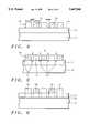
Referring to FIG. 1, there is shown a portion of a partially completed integrated circuit. Alayer 12 which is to be etched is deposited oversilicon substrate 10.Photoresist layer 14 coats the surface of thelayer 12. As shown in FIG. 1, thephotoresist layer 14 is patterned to create a photoresist mask. If the resolution of the photolithography process is R and the minimum misalignment tolerance between two layers is M, then the minimum pitch (line width (15)+line spacing (16)) is R+R=2R, by the conventional photolithographic process of the prior art.
U.S. Pat. No. 4,906,552 to Ngo et al describes a flood illumination patterning technique that achieves resolutions of 0.5 micrometers or less using a dual layer of photoresist. U.S. Pat. Nos. 5,091,290 to Rolfson, 4,704,347 to Vollenbroek et al, and 4,591,547 to Brownell all teach methods of dual layers of photoresist in which one layer of photoresist is at least partially over the other layer of photoresist.
A principal object of the present invention is to provide an effective and very manufacturable method of providing narrow line spacing of less than the resolution limit of the photolithography process.
In accordance with the object of this invention a new photolithographic process using the method of photoresist double coating to fabricate fine lines with narrow spacing is achieved. A layer to be etched is provided overlying a semiconductor substrate. The layer to be etched is coated with a first layer of photoresist and baked. The first photoresist layer is exposed to actinic light through openings in a mask and developed to produce the desired first pattern on the surface of the first photoresist wherein the openings have a minimum width of the resolution limit plus two times the misalignment tolerance of the photolithography process. The layer to be etched is coated with a second photoresist layer where the layer to be etched is exposed within the openings in the first photoresist layer. The second photoresist layer is exposed to actinic light through openings in a mask and developed to produce the desired second pattern on the surface of the second photoresist wherein the second pattern alternates with the first photoresist pattern and wherein the spacing between the first and second patterned photoresist coatings has a width equal to the misalignment tolerance. The misalignment tolerance is much smaller than the resolution limit so the line spacing achieved is narrower than the resolution limit of the photolithography process.
In the accompanying drawings forming a material part of this description, there is shown:
FIG. 1 schematically illustrates in cross-sectional representation a photolithographic process of the prior art.
FIGS. 2 through 4 schematically illustrate in cross-sectional representation a preferred embodiment of the present invention.
FIGS. 5 through 8 schematically illustrate in cross-sectional representation additional embodiments of the present invention.
FIG. 9 schematically illustrates in cross-sectional representation a completed integrated circuit for one embodiment of the present invention.
Referring now more particularly to FIGS. 2 through 4, the photolithographic method of the present invention will be described. Alayer 12 to be etched has been deposited over the surface ofsemiconductor substrate 10. This layer can be a single layer or multi-layers and can be a polysilicon word line or metal line or various other structures in the fabrication of an integrated circuit. Specific examples will be discussed in the Examples section to follow. The process of the invention is independent of the material to be etched.
A first layer ofphotoresist 14 is coated over the surface of thelayer 12. A positive photoresist is used with a conventional thickness of between about 10,000 to 30,000 Angstroms. Thephotoresist layer 14 is exposed to actinic light through openings in a mask and developed to produce the desired pattern on the surface of the photoresist. The resultingresist mask layer 14 has openings of the size R+2M, where R is the line width and M is the misalignment tolerance.
Thephotoresist mask layer 14 is baked using an ultraviolet baking process at a temperature of between about 140° to 160° C. for between about 50 to 70 seconds. The ultraviolet baking process hardens the photoresist mask layer.
A secondphotoresist coating 18 is spun onto the wafer into the openings in thephotoresist mask layer 14. Thephotoresist layer 18 is exposed to actinic light through openings in amask 20, shown in FIG. 3, and developed to produce the desired pattern on the surface of the photoresist. Since the firstphotoresist mask 14 has been hardened by the ultraviolet baking process, it will not be removed during developing and etching of thesecond photoresist layer 18. The resulting resist mask layer is illustrated in FIG. 4. The spacing between the lines will be M instead of R as in the prior art. Since M is much smaller than R, the line spacing has been reduced dramatically by using the double photoresist coating method of the invention. For example, for the 0.6 micrometer design rule, R=0.6 micrometers and M is approximately=0.2 micrometers. After thelayer 12 has been etched, thephotoresist mask layer
The following Examples are given to show the important features of the invention and to aid in the understanding thereof and variations may be made by one skilled in the art without departing from the spirit and scope of the invention.
The following Examples will illustrate some applications for the double photoresist coating process of the invention. Referring now to FIG. 5, there is illustrated a buried bit mask read-only memory (ROM) process. Thedouble photoresist mask silicon substrate 10. AnN+ ion implantation 19 into thesubstrate 10 through the openings in the photoresist mask forms buriedbit lines 21. This process allows the designer to reduce the buried bit line openings and thus reduce the cell size of the memory.
Referring now to FIG. 6, there is illustrated another buried bit mask ROM process in which polysilicon word lines are to be fabricated. A gatesilicon oxide layer 22 has been grown or deposited over the surface of thesilicon substrate 10. A layer ofpolysilicon 24 is deposited over the surface of the silicon oxide. Thephotoresist mask polysilicon layer 24. Reducing the space between the word lines will reduce the cell size of the memory. FIG. 9 illustrates the completed integrated circuit of this example showing the word lines 24 andpassivation layer 30 of, for example, borophosphosilicate glass.
FIG. 7 illustrates a buried bit line or a NAND-typed double polysilicon erasable-programmable read-only memory (EPROM) or a Flash memory. A gate silicon oxide or tunnelsilicon oxide layer 32 is grown or deposited on the surface of thesilicon substrate 10.Layer 34 is a polysilicon floating gate layer. Aninterpoly dielectric layer 36 is deposited over the floatinggate 34. Thislayer 36 is typically composed of a multiple ONO layer consisting of silicon oxide, silicon nitride, and silicon oxide. Finally, the controlgate polysilicon layer 38 is deposited over the ONO layer. Thedouble photoresist mask layers
FIG. 8 illustrates metal line definition. Thesemiconductor substrate 10, which may contain semiconductor device structures such as gate electrodes and source and drain regions, is covered with an insulatinglayer 42 composed of borophosphosilicate glass (BPSG), for example. Ametal layer 44 is deposited over the BPSG layer. Thedouble photoresist mask metal 44 and is used to etch metal lines as indicated by the dotted lines withinlayer 44 in FIG. 8.
The double photoresist coating method of the invention may be used in etching active isolation regions and in other etching applications in the manufacture of integrated circuits.
While the invention has been particularly shown and described with reference to the preferred embodiments thereof, it will be understood by those skilled in the art that various changes in form and details may be made without departing from the spirit and scope of the invention.
Claims (20)
1. A method of forming a double coating photoresist mask to allow line spacing narrower than the photolithography resolution limit in the fabrication of an integrated circuit comprising:
providing a semiconductor substrate including a layer to be etched;
coating said layer to be etched with a first layer of photoresist;
exposing said first photoresist layer to light through a mask, developing said first photoresist layer and removing parts of said first photoresist layer to produce a first pattern from said first photoresist layer having first openings wider than said resolution limit, said first openings flee of photoresist from said first photoresist layer;
hardening said first patterned photoresist layer;
coating said layer to be etched with a second photoresist layer so that said second photoresist layer is within said first openings in said first patterned photoresist layer;
exposing said second photoresist layer to light through a mask, developing said second photoresist layer and removing parts of said second photoresist layer to produce a second pattern from said second photoresist layer having portions of said second pattern within said first openings,
said portions of said second pattern within said first openings having first and second edges on opposing sides of said portion, a first edge separated from said first patterned photoresist layer by a first region of the layer to be etched, and a second edge separated from said first patterned photoresist layer by a second region of the layer to be etched,
said first and second regions of the layer to be etched lying within said first opening; and
wherein at least some of said first and second regions are narrower than said resolution limit of said photolithography process.
2. The method of claim 1, wherein said first patterned photoresist layer is formed on said layer to be etched.
3. The method of claim 2, wherein said second pattern is formed on said layer to be etched.
4. The method of claim 1 wherein said layer to be etched is a stacked gate layer consisting of a polysilicon control gate overlying a dielectric layer overlying a polysilicon floating gate layer.
5. The method of claim 1 wherein said layer to be etched is a metal layer.
6. A method of forming a double coating photoresist mask to allow line widths narrower than the photolithography resolution limit in the fabrication of an integrated circuit comprising:
coating a semiconductor substrate with a first layer of photoresist;
exposing said first photoresist layer to light through a mask, developing said first photoresist layer and removing parts of said first photoresist layer to produce a first patterned photoresist layer having first openings wider than said resolution limit, said first openings free of said first photoresist layer;
hardening said first patterned photoresist layer;
coating said semiconductor substrate with a second photoresist layer so that said second photoresist layer is within said first openings in said first patterned photoresist layer;
exposing said second photoresist layer to light through a mask, developing said second photoresist layer and removing parts of said second photoresist layer to produce a second pattern from said second photoresist layer wherein said second pattern lies within said first openings in said first patterned photoresist layer so that regions of said first patterned photoresist layer are interleaved with regions of said second pattern laterally across at least a portion of said semiconductor substrate, leaving portions of said semiconductor substrate not covered with photoresist between adjacent regions of said first patterned photoresist layer and said second pattern.
7. A method as in claim 6 for forming a double coating resist mask used to form buried bit lines narrower than the photolithography resolution limit, the method further comprising the step of implanting ions into said portions of said semiconductor substrate not covered with photoresist to form said buried bit lines narrower than said resolution limit of said photolithography process.
8. A method as in claim 6, comprising the step of etching said semiconductor substrate not covered by said first and second patterned photoresist layers to form a device having at least some lines narrower than said resolution limit of said photolithography process.
9. A method of forming a double coating photoresist mask to allow for line spacing narrower than the photolithography resolution limit in the fabrication of an integrated circuit comprising:
providing at least one layer to be etched overlying a semiconductor substrate;
coating said layer to be etched with a first layer of photoresist;
exposing said first photoresist layer to light through a mask, developing said first photoresist layer and removing parts of said first photoresist layer to produce a first patterned photoresist layer having first openings wider than said resolution limit as measured along a first direction, said first openings free of photoresist from said first photoresist layer;
hardening said first patterned photoresist layer;
coating said layer to be etched with a second photoresist layer so that said second photoresist layer is within said first openings in said first patterned photoresist layer; and
exposing said second photoresist layer to light through a mask, developing said second photoresist layer and removing parts of said second photoresist layer to produce a second pattern from said second photoresist layer which lies within said first openings in said first patterned photoresist layer so that regions of said first patterned photoresist layer are interleaved with regions of said second pattern laterally along said first direction across at least a portion of said layer to be etched, leaving said layer to be etched not covered with photoresist between adjacent regions of said first patterned photoresist layer and said second pattern.
10. A method as in claim 9 for forming a double coating photoresist mask to allow word line spacing narrower than the photolithography resolution limit in the fabrication of an integrated circuit:
wherein said layer to be etched is formed by providing a gate silicon oxide layer over the surface of said semiconductor substrate and depositing a polysilicon layer over said gate silicon oxide layer; and
etching said polysilicon layer not covered by said first and second patterned photoresist layers to form polysilicon word line spacing narrower than said photolithography resolution limit.
11. A method as in claim 9 wherein said first photoresist layer is baked under ultraviolet light at a temperature of between about 140° to 160° C. for between about 50 to 70 seconds.
12. A method as in claim 9 for forming a double coating photoresist mask to allow metal line spacing narrower than the photolithography resolution limit in the fabrication of an integrated circuit:
wherein said layer to be etched is formed by providing an insulating layer overlying said semiconductor substrate and depositing a metal layer overlying said insulating layer;
etching said metal layer not covered by said first and second patterned photoresist layers wherein said metal line spacing achieved is narrower than said resolution limit of said photolithography process.
13. The method of claim 9 wherein said layer to be etched is a polysilicon layer.
14. The method of claim 9 wherein said layer to be etched is a stacked gate layer consisting of a polysilicon control gate overlying a dielectric layer overlying a polysilicon floating gate layer.
15. The method of claim 9 wherein said layer to be etched is a metal layer.
16. The method of claim 9 wherein said first openings have a minimum width of the resolution limit of the photolithography process plus two times the misalignment tolerance of said photolithography process and wherein said second photoresist pattern alternates with said first photoresist pattern and wherein the spacing between said first and second patterned photoresist coatings has a width equal to said misalignment tolerance wherein said misalignment tolerance is smaller than said resolution limit and wherein the line spacing achieved is smaller than said resolution limit of said photolithography process.
17. A method as in claim 9 for forming a double coating photoresist mask to allow line spacing of a stacked gate memory narrower than the photolithography resolution limit in the fabrication of an integrated circuit:
wherein said layer to be etched is formed by providing an insulating layer over the surface of said semiconductor substrate, depositing a polysilicon floating gate layer overlying said insulating layer, depositing an interpoly dielectric layer overlying said polysilicon floating gate layer and depositing a control gate polysilicon layer overlying said interpoly dielectric layer; and
etching said polysilicon control gate layer, said interpoly dielectric layer, and said polysilicon floating gate layer not covered by said first and second patterned photoresist layers to form said stacked gate structures wherein said line spacings achieved are narrower than said photolithography resolution limit.
18. The method of claim 17 wherein said insulating layer is composed of a gate silicon oxide.
19. The method of claim 17 wherein said insulating layer is composed of a tunnel silicon oxide.
20. The method of claim 17 wherein said interpoly dielectric layer is composed of silicon oxide, silicon nitride, and silicon oxide layers.
Priority Applications (1)
| Application Number | Priority Date | Filing Date | Title |
|---|---|---|---|
| US08/746,147US5667940A (en) | 1994-05-11 | 1996-11-06 | Process for creating high density integrated circuits utilizing double coating photoresist mask |
Applications Claiming Priority (2)
| Application Number | Priority Date | Filing Date | Title |
|---|---|---|---|
| US24133694A | 1994-05-11 | 1994-05-11 | |
| US08/746,147US5667940A (en) | 1994-05-11 | 1996-11-06 | Process for creating high density integrated circuits utilizing double coating photoresist mask |
Related Parent Applications (1)
| Application Number | Title | Priority Date | Filing Date |
|---|---|---|---|
| US24133694AContinuation | 1994-05-11 | 1994-05-11 |
Publications (1)
| Publication Number | Publication Date |
|---|---|
| US5667940Atrue US5667940A (en) | 1997-09-16 |
Family
ID=22910301
Family Applications (1)
| Application Number | Title | Priority Date | Filing Date |
|---|---|---|---|
| US08/746,147Expired - Fee RelatedUS5667940A (en) | 1994-05-11 | 1996-11-06 | Process for creating high density integrated circuits utilizing double coating photoresist mask |
Country Status (1)
| Country | Link |
|---|---|
| US (1) | US5667940A (en) |
Cited By (46)
| Publication number | Priority date | Publication date | Assignee | Title |
|---|---|---|---|---|
| US5763955A (en)* | 1996-07-01 | 1998-06-09 | Vlsi Technology, Inc. | Patterned filled layers for integrated circuit manufacturing |
| US5811223A (en)* | 1995-04-10 | 1998-09-22 | Hyundai Electronics Industries Co., Ltd. | Method for inspecting process defects occurring in semiconductor devices |
| US5817445A (en)* | 1995-10-04 | 1998-10-06 | Hyundai Electronics Industries, Co., Ltd. | Method for inspecting process defects occurring in semiconductor devices |
| US5945259A (en)* | 1997-05-12 | 1999-08-31 | Samsung Aerospace Industries, Ltd. | Method for lead frame etching |
| US6329124B1 (en) | 1999-05-26 | 2001-12-11 | Advanced Micro Devices | Method to produce high density memory cells and small spaces by using nitride spacer |
| EP1045289A3 (en)* | 1999-04-16 | 2002-05-29 | Lucent Technologies Inc. | A lithographic process having sub-wavelength resolution |
| US6409312B1 (en) | 2001-03-27 | 2002-06-25 | Lexmark International, Inc. | Ink jet printer nozzle plate and process therefor |
| US6416933B1 (en) | 1999-04-01 | 2002-07-09 | Advanced Micro Devices, Inc. | Method to produce small space pattern using plasma polymerization layer |
| US6528238B1 (en)* | 2000-09-22 | 2003-03-04 | David Seniuk | Methods for making patterns in radiation sensitive polymers |
| US6548224B1 (en)* | 2000-03-07 | 2003-04-15 | Kulicke & Soffa Holdings, Inc. | Wiring substrate features having controlled sidewall profiles |
| US6617098B1 (en)* | 1999-07-13 | 2003-09-09 | Input/Output, Inc. | Merged-mask micro-machining process |
| US6632592B1 (en)* | 1999-09-09 | 2003-10-14 | Kabushiki Kaisha Toshiba | Resist pattern forming method |
| US6664028B2 (en)* | 2000-12-04 | 2003-12-16 | United Microelectronics Corp. | Method of forming opening in wafer layer |
| US20030232252A1 (en)* | 2002-06-18 | 2003-12-18 | Mancini David P. | Multi-tiered lithographic template and method of formation and use |
| US6849462B1 (en) | 1991-11-22 | 2005-02-01 | Affymetrix, Inc. | Combinatorial strategies for polymer synthesis |
| US6943034B1 (en) | 1991-11-22 | 2005-09-13 | Affymetrix, Inc. | Combinatorial strategies for polymer synthesis |
| US20060127816A1 (en)* | 2004-12-10 | 2006-06-15 | Samsung Electronics Co., Ltd. | Double photolithography methods with reduced intermixing of solvents |
| US20070072094A1 (en)* | 2004-04-01 | 2007-03-29 | Matrix Semiconductor, Inc. | Photomask features with chromeless nonprinting phase shifting window |
| US20070148983A1 (en)* | 2005-12-28 | 2007-06-28 | Hynix Semiconductor Inc. | Method for Manufacturing Semiconductor Device |
| US20080044772A1 (en)* | 2006-08-18 | 2008-02-21 | Guerrero Douglas J | Anti-reflective imaging layer for multiple patterning process |
| RU2325000C1 (en)* | 2006-11-20 | 2008-05-20 | Государственное образовательное учреждение высшего профессионального образования "Мордовский государственный университет им. Н.П. Огарева" | Method of photolithography |
| US20090011374A1 (en)* | 2005-08-24 | 2009-01-08 | Ching-Yu Chang | Method and material for forming high etch resistant double exposure patterns |
| WO2009067354A1 (en) | 2007-11-19 | 2009-05-28 | International Business Machines Corporation | Photoresist compositions and process for multiple exposures with multiple layer photoresist systems |
| US20090142701A1 (en)* | 2007-11-30 | 2009-06-04 | Taiwan Semiconductor Manufacturing Company, Ltd. | Double patterning strategy for contact hole and trench |
| US20090155962A1 (en)* | 2007-12-17 | 2009-06-18 | Sandisk 3D Llc | Method for fabricating pitch-doubling pillar structures |
| US20090233238A1 (en)* | 2008-03-12 | 2009-09-17 | Taiwan Semiconductor Manufacturing Company, Ltd. | Double Patterning Strategy For Contact Hole and Trench in Photolithography |
| WO2009126490A1 (en)* | 2008-04-11 | 2009-10-15 | Sandisk 3D Llc | Double patterning method |
| US20090258318A1 (en)* | 2008-04-11 | 2009-10-15 | Sandisk 3D Llc | Double patterning method |
| US20090269932A1 (en)* | 2008-04-28 | 2009-10-29 | Sandisk 3D Llc | Method for fabricating self-aligned complimentary pillar structures and wiring |
| US20090325379A1 (en)* | 2008-06-30 | 2009-12-31 | Hlad Mark S | Methods for fabricating fine line/space (fls) routing in high density interconnect (hdi) substrates |
| US20100310995A1 (en)* | 2009-02-11 | 2010-12-09 | Taiwan Semiconductor Manufacturing Company, Ltd. | Double patterning strategy for contact hole and trench in photolithography |
| US20110003253A1 (en)* | 2009-07-06 | 2011-01-06 | Sony Corporation | Method of manufacturing semiconductor device and pattern formation method |
| US20110059407A1 (en)* | 2009-09-09 | 2011-03-10 | Taiwan Semiconductor Manufacturing Company, Ltd. | Double patterning strategy for forming fine patterns in photolithography |
| US20110171815A1 (en)* | 2010-01-12 | 2011-07-14 | Sandisk 3D Llc | Patterning method for high density pillar structures |
| CN102147568A (en)* | 2010-02-09 | 2011-08-10 | 台湾积体电路制造股份有限公司 | Photoetching patterning method and double patterning method |
| US20110281220A1 (en)* | 2010-05-11 | 2011-11-17 | Takashi Matsuda | Pattern formation method |
| US8133659B2 (en) | 2008-01-29 | 2012-03-13 | Brewer Science Inc. | On-track process for patterning hardmask by multiple dark field exposures |
| CN103441098A (en)* | 2013-09-12 | 2013-12-11 | 江阴长电先进封装有限公司 | Simple preparation method of wafer-level high-density wiring |
| CN104282613A (en)* | 2013-07-02 | 2015-01-14 | 中芯国际集成电路制造(上海)有限公司 | Semiconductor manufacturing method |
| US20150243504A1 (en)* | 2011-10-20 | 2015-08-27 | Taiwan Semiconductor Manufacturing Company, Ltd. | Method of forming an integrated circuit |
| US20160064393A1 (en)* | 2006-06-27 | 2016-03-03 | Kabushiki Kaisha Toshiba | Nonvolatile semiconductor memory having a word line bent towards a select gate line side |
| US20170025401A1 (en)* | 2013-06-28 | 2017-01-26 | Taiwan Semiconductor Manufacturing Company, Ltd. | Conductive Line Patterning |
| WO2017058589A1 (en)* | 2015-09-30 | 2017-04-06 | Tokyo Electron Limited | Method for patterning a substrate using extreme ultraviolet lithography |
| US9640396B2 (en) | 2009-01-07 | 2017-05-02 | Brewer Science Inc. | Spin-on spacer materials for double- and triple-patterning lithography |
| WO2017087066A1 (en)* | 2015-11-20 | 2017-05-26 | Tokyo Electron Limited | Methods of forming etch masks for sub-resolution substrate patterning |
| US11037820B2 (en)* | 2017-09-29 | 2021-06-15 | Taiwan Semiconductor Manufacturing Co., Ltd. | Method for forming vias and method for forming contacts in vias |
Citations (4)
| Publication number | Priority date | Publication date | Assignee | Title |
|---|---|---|---|---|
| US4591547A (en)* | 1982-10-20 | 1986-05-27 | General Instrument Corporation | Dual layer positive photoresist process and devices |
| US4704347A (en)* | 1985-02-18 | 1987-11-03 | U.S. Philips Corporation | Method of manufacturing a semiconductor device, in which a photolacquer mask is formed by means of a two-layer lacquer system. |
| US4906552A (en)* | 1988-02-22 | 1990-03-06 | Hughes Aircraft Company | Two layer dye photoresist process for sub-half micrometer resolution photolithography |
| US5091290A (en)* | 1990-12-03 | 1992-02-25 | Micron Technology, Inc. | Process for promoting adhesion of a layer of photoresist on a substrate having a previous layer of photoresist |
- 1996
- 1996-11-06USUS08/746,147patent/US5667940A/ennot_activeExpired - Fee Related
Patent Citations (4)
| Publication number | Priority date | Publication date | Assignee | Title |
|---|---|---|---|---|
| US4591547A (en)* | 1982-10-20 | 1986-05-27 | General Instrument Corporation | Dual layer positive photoresist process and devices |
| US4704347A (en)* | 1985-02-18 | 1987-11-03 | U.S. Philips Corporation | Method of manufacturing a semiconductor device, in which a photolacquer mask is formed by means of a two-layer lacquer system. |
| US4906552A (en)* | 1988-02-22 | 1990-03-06 | Hughes Aircraft Company | Two layer dye photoresist process for sub-half micrometer resolution photolithography |
| US5091290A (en)* | 1990-12-03 | 1992-02-25 | Micron Technology, Inc. | Process for promoting adhesion of a layer of photoresist on a substrate having a previous layer of photoresist |
Cited By (96)
| Publication number | Priority date | Publication date | Assignee | Title |
|---|---|---|---|---|
| US6943034B1 (en) | 1991-11-22 | 2005-09-13 | Affymetrix, Inc. | Combinatorial strategies for polymer synthesis |
| US6849462B1 (en) | 1991-11-22 | 2005-02-01 | Affymetrix, Inc. | Combinatorial strategies for polymer synthesis |
| US7736906B2 (en) | 1991-11-22 | 2010-06-15 | Affymetrix, Inc. | Combinatorial strategies for polymer synthesis |
| US7691330B1 (en) | 1991-11-22 | 2010-04-06 | Affymetrix, Inc. | Combinatorial strategies for polymer synthesis |
| US6864101B1 (en) | 1991-11-22 | 2005-03-08 | Affymetrix, Inc. | Combinatorial strategies for polymer synthesis |
| US5811223A (en)* | 1995-04-10 | 1998-09-22 | Hyundai Electronics Industries Co., Ltd. | Method for inspecting process defects occurring in semiconductor devices |
| US5817445A (en)* | 1995-10-04 | 1998-10-06 | Hyundai Electronics Industries, Co., Ltd. | Method for inspecting process defects occurring in semiconductor devices |
| US5763955A (en)* | 1996-07-01 | 1998-06-09 | Vlsi Technology, Inc. | Patterned filled layers for integrated circuit manufacturing |
| US5945259A (en)* | 1997-05-12 | 1999-08-31 | Samsung Aerospace Industries, Ltd. | Method for lead frame etching |
| US6416933B1 (en) | 1999-04-01 | 2002-07-09 | Advanced Micro Devices, Inc. | Method to produce small space pattern using plasma polymerization layer |
| EP1045289A3 (en)* | 1999-04-16 | 2002-05-29 | Lucent Technologies Inc. | A lithographic process having sub-wavelength resolution |
| US6329124B1 (en) | 1999-05-26 | 2001-12-11 | Advanced Micro Devices | Method to produce high density memory cells and small spaces by using nitride spacer |
| US6617098B1 (en)* | 1999-07-13 | 2003-09-09 | Input/Output, Inc. | Merged-mask micro-machining process |
| US6632592B1 (en)* | 1999-09-09 | 2003-10-14 | Kabushiki Kaisha Toshiba | Resist pattern forming method |
| US6548224B1 (en)* | 2000-03-07 | 2003-04-15 | Kulicke & Soffa Holdings, Inc. | Wiring substrate features having controlled sidewall profiles |
| US6528238B1 (en)* | 2000-09-22 | 2003-03-04 | David Seniuk | Methods for making patterns in radiation sensitive polymers |
| US6664028B2 (en)* | 2000-12-04 | 2003-12-16 | United Microelectronics Corp. | Method of forming opening in wafer layer |
| US6409312B1 (en) | 2001-03-27 | 2002-06-25 | Lexmark International, Inc. | Ink jet printer nozzle plate and process therefor |
| WO2003107094A1 (en)* | 2002-06-18 | 2003-12-24 | Motorola, Inc. | Multi-tiered lithographic template |
| JP2005530338A (en)* | 2002-06-18 | 2005-10-06 | フリースケール セミコンダクター インコーポレイテッド | Multistage lithographic template |
| US6852454B2 (en) | 2002-06-18 | 2005-02-08 | Freescale Semiconductor, Inc. | Multi-tiered lithographic template and method of formation and use |
| CN1662852B (en)* | 2002-06-18 | 2010-10-27 | 飞思卡尔半导体公司 | Multi-layer lithographic template |
| US20030232252A1 (en)* | 2002-06-18 | 2003-12-18 | Mancini David P. | Multi-tiered lithographic template and method of formation and use |
| US20070072094A1 (en)* | 2004-04-01 | 2007-03-29 | Matrix Semiconductor, Inc. | Photomask features with chromeless nonprinting phase shifting window |
| US7494765B2 (en)* | 2004-04-01 | 2009-02-24 | Sandisk 3D Llc | Method for patterning photoresist pillars using a photomask having a plurality of chromeless nonprinting phase shifting windows |
| US20060127816A1 (en)* | 2004-12-10 | 2006-06-15 | Samsung Electronics Co., Ltd. | Double photolithography methods with reduced intermixing of solvents |
| US8153350B2 (en)* | 2005-08-24 | 2012-04-10 | Taiwan Semiconductor Manufacturing Co., Ltd. | Method and material for forming high etch resistant double exposure patterns |
| US20090011374A1 (en)* | 2005-08-24 | 2009-01-08 | Ching-Yu Chang | Method and material for forming high etch resistant double exposure patterns |
| US20070148983A1 (en)* | 2005-12-28 | 2007-06-28 | Hynix Semiconductor Inc. | Method for Manufacturing Semiconductor Device |
| US7655568B2 (en) | 2005-12-28 | 2010-02-02 | Hynix Semiconductor Inc. | Method for manufacturing underlying pattern of semiconductor device |
| US20160064393A1 (en)* | 2006-06-27 | 2016-03-03 | Kabushiki Kaisha Toshiba | Nonvolatile semiconductor memory having a word line bent towards a select gate line side |
| TWI453792B (en)* | 2006-08-18 | 2014-09-21 | Brewer Science Inc | Anti-reflective imaging layer for multiple patterning process |
| US20080044772A1 (en)* | 2006-08-18 | 2008-02-21 | Guerrero Douglas J | Anti-reflective imaging layer for multiple patterning process |
| US7914974B2 (en)* | 2006-08-18 | 2011-03-29 | Brewer Science Inc. | Anti-reflective imaging layer for multiple patterning process |
| RU2325000C1 (en)* | 2006-11-20 | 2008-05-20 | Государственное образовательное учреждение высшего профессионального образования "Мордовский государственный университет им. Н.П. Огарева" | Method of photolithography |
| EP2212905A4 (en)* | 2007-11-19 | 2012-03-07 | Ibm | Photoresist compositions and process for multiple exposures with multiple layer photoresist systems |
| WO2009067354A1 (en) | 2007-11-19 | 2009-05-28 | International Business Machines Corporation | Photoresist compositions and process for multiple exposures with multiple layer photoresist systems |
| US20100248147A1 (en)* | 2007-11-19 | 2010-09-30 | International Business Machines Corporation | Photoresist compositions and process for multiple exposures with multiple layer photoresist systems |
| CN101861638A (en)* | 2007-11-19 | 2010-10-13 | 国际商业机器公司 | Photoresist compositions and process for multiple exposures with multiple layer photoresist systems |
| CN101446760B (en)* | 2007-11-30 | 2012-01-18 | 台湾积体电路制造股份有限公司 | Lithography Double Patterning Method |
| US9323155B2 (en) | 2007-11-30 | 2016-04-26 | Taiwan Semiconductor Manufacturing Company, Ltd. | Double patterning strategy for contact hole and trench in photolithography |
| US7935477B2 (en)* | 2007-11-30 | 2011-05-03 | Taiwan Semiconductor Manufacturing Company, Ltd. | Double patterning strategy for contact hole and trench |
| US20090142701A1 (en)* | 2007-11-30 | 2009-06-04 | Taiwan Semiconductor Manufacturing Company, Ltd. | Double patterning strategy for contact hole and trench |
| TWI424469B (en)* | 2007-11-30 | 2014-01-21 | Taiwan Semiconductor Mfg | Double patterning strategy for contact hole and trench |
| US20090155962A1 (en)* | 2007-12-17 | 2009-06-18 | Sandisk 3D Llc | Method for fabricating pitch-doubling pillar structures |
| US7759201B2 (en) | 2007-12-17 | 2010-07-20 | Sandisk 3D Llc | Method for fabricating pitch-doubling pillar structures |
| US8415083B2 (en) | 2008-01-29 | 2013-04-09 | Brewer Science Inc. | On-track process for patterning hardmask by multiple dark field exposures |
| US8133659B2 (en) | 2008-01-29 | 2012-03-13 | Brewer Science Inc. | On-track process for patterning hardmask by multiple dark field exposures |
| US8450052B2 (en) | 2008-03-12 | 2013-05-28 | Taiwan Semiconductor Manufacturing Company, Ltd. | Double patterning strategy for contact hole and trench in photolithography |
| US8048616B2 (en) | 2008-03-12 | 2011-11-01 | Taiwan Semiconductor Manufacturing Company, Ltd. | Double patterning strategy for contact hole and trench in photolithography |
| US20090233238A1 (en)* | 2008-03-12 | 2009-09-17 | Taiwan Semiconductor Manufacturing Company, Ltd. | Double Patterning Strategy For Contact Hole and Trench in Photolithography |
| US7713818B2 (en) | 2008-04-11 | 2010-05-11 | Sandisk 3D, Llc | Double patterning method |
| US7981592B2 (en) | 2008-04-11 | 2011-07-19 | Sandisk 3D Llc | Double patterning method |
| US8178286B2 (en) | 2008-04-11 | 2012-05-15 | Sandisk 3D Llc | Double patterning method |
| US20110236833A1 (en)* | 2008-04-11 | 2011-09-29 | Sandisk 3D Llc | Double Patterning Method |
| WO2009126490A1 (en)* | 2008-04-11 | 2009-10-15 | Sandisk 3D Llc | Double patterning method |
| US20090258501A1 (en)* | 2008-04-11 | 2009-10-15 | Sandisk 3D Llc | Double patterning method |
| US20090258318A1 (en)* | 2008-04-11 | 2009-10-15 | Sandisk 3D Llc | Double patterning method |
| US7786015B2 (en) | 2008-04-28 | 2010-08-31 | Sandisk 3D Llc | Method for fabricating self-aligned complementary pillar structures and wiring |
| US20090269932A1 (en)* | 2008-04-28 | 2009-10-29 | Sandisk 3D Llc | Method for fabricating self-aligned complimentary pillar structures and wiring |
| US7919408B2 (en)* | 2008-06-30 | 2011-04-05 | Intel Corporation | Methods for fabricating fine line/space (FLS) routing in high density interconnect (HDI) substrates |
| US20090325379A1 (en)* | 2008-06-30 | 2009-12-31 | Hlad Mark S | Methods for fabricating fine line/space (fls) routing in high density interconnect (hdi) substrates |
| US9640396B2 (en) | 2009-01-07 | 2017-05-02 | Brewer Science Inc. | Spin-on spacer materials for double- and triple-patterning lithography |
| US8741552B2 (en)* | 2009-02-11 | 2014-06-03 | Taiwan Semiconductor Manufacturing Company, Ltd. | Double patterning strategy for contact hole and trench in photolithography |
| US20100310995A1 (en)* | 2009-02-11 | 2010-12-09 | Taiwan Semiconductor Manufacturing Company, Ltd. | Double patterning strategy for contact hole and trench in photolithography |
| US8445183B2 (en)* | 2009-07-06 | 2013-05-21 | Sony Corporation | Method of manufacturing semiconductor device and pattern formation method |
| US20110003253A1 (en)* | 2009-07-06 | 2011-01-06 | Sony Corporation | Method of manufacturing semiconductor device and pattern formation method |
| US20110059407A1 (en)* | 2009-09-09 | 2011-03-10 | Taiwan Semiconductor Manufacturing Company, Ltd. | Double patterning strategy for forming fine patterns in photolithography |
| US8026178B2 (en) | 2010-01-12 | 2011-09-27 | Sandisk 3D Llc | Patterning method for high density pillar structures |
| US20110171815A1 (en)* | 2010-01-12 | 2011-07-14 | Sandisk 3D Llc | Patterning method for high density pillar structures |
| US8241969B2 (en) | 2010-01-12 | 2012-08-14 | Sandisk 3D Llc | Patterning method for high density pillar structures |
| US8329512B2 (en) | 2010-01-12 | 2012-12-11 | Sandisk 3D Llc | Patterning method for high density pillar structures |
| CN102147568A (en)* | 2010-02-09 | 2011-08-10 | 台湾积体电路制造股份有限公司 | Photoetching patterning method and double patterning method |
| US8445184B2 (en)* | 2010-05-11 | 2013-05-21 | Panasonic Corporation | Pattern formation method |
| US20110281220A1 (en)* | 2010-05-11 | 2011-11-17 | Takashi Matsuda | Pattern formation method |
| US11462408B2 (en) | 2011-10-20 | 2022-10-04 | Taiwan Semiconductor Manufacturing Company, Ltd. | Method of forming an integrated circuit using a patterned mask layer |
| US20150243504A1 (en)* | 2011-10-20 | 2015-08-27 | Taiwan Semiconductor Manufacturing Company, Ltd. | Method of forming an integrated circuit |
| US10665457B2 (en) | 2011-10-20 | 2020-05-26 | Taiwan Semiconductor Manufacturing Company, Ltd. | Method of forming an integrated circuit using a patterned mask layer |
| US12027370B2 (en) | 2011-10-20 | 2024-07-02 | Taiwan Semiconductor Manufacturing Company, Ltd. | Method of forming an integrated circuit using a patterned mask layer |
| US9934971B2 (en) | 2011-10-20 | 2018-04-03 | Taiwan Semiconductor Manufacturing Company, Ltd. | Method of forming an integrated circuit using a patterned mask layer |
| US9640398B2 (en)* | 2011-10-20 | 2017-05-02 | Taiwan Semiconductor Manufacturing Company, Ltd. | Method of forming an integrated circuit using a patterned mask layer |
| US10269785B2 (en)* | 2013-06-28 | 2019-04-23 | Taiwan Semiconductor Manufacturing Company, Ltd. | Conductive line patterning |
| US10998304B2 (en) | 2013-06-28 | 2021-05-04 | Taiwan Semiconductor Manufacturing Company, Ltd. | Conductive line patterning |
| US20170025401A1 (en)* | 2013-06-28 | 2017-01-26 | Taiwan Semiconductor Manufacturing Company, Ltd. | Conductive Line Patterning |
| CN104282613B (en)* | 2013-07-02 | 2017-08-25 | 中芯国际集成电路制造(上海)有限公司 | Semiconductor making method |
| CN104282613A (en)* | 2013-07-02 | 2015-01-14 | 中芯国际集成电路制造(上海)有限公司 | Semiconductor manufacturing method |
| CN103441098A (en)* | 2013-09-12 | 2013-12-11 | 江阴长电先进封装有限公司 | Simple preparation method of wafer-level high-density wiring |
| US10606176B2 (en) | 2015-09-30 | 2020-03-31 | Tokyo Electron Limited | Method for patterning a substrate using extreme ultraviolet lithography |
| TWI625602B (en)* | 2015-09-30 | 2018-06-01 | 東京威力科創股份有限公司 | Method for patterning a substrate using extreme ultraviolet lithography |
| KR20180050425A (en)* | 2015-09-30 | 2018-05-14 | 도쿄엘렉트론가부시키가이샤 | Method for patterning a substrate using extreme ultraviolet lithography |
| WO2017058589A1 (en)* | 2015-09-30 | 2017-04-06 | Tokyo Electron Limited | Method for patterning a substrate using extreme ultraviolet lithography |
| US10103032B2 (en) | 2015-11-20 | 2018-10-16 | Tokyo Electron Limited | Methods of forming etch masks for sub-resolution substrate patterning |
| WO2017087066A1 (en)* | 2015-11-20 | 2017-05-26 | Tokyo Electron Limited | Methods of forming etch masks for sub-resolution substrate patterning |
| US11037820B2 (en)* | 2017-09-29 | 2021-06-15 | Taiwan Semiconductor Manufacturing Co., Ltd. | Method for forming vias and method for forming contacts in vias |
| US20210313220A1 (en)* | 2017-09-29 | 2021-10-07 | Taiwan Semiconductor Manufacturing Company, Ltd. | Method for forming vias and method for forming contacts in vias |
| US11581217B2 (en)* | 2017-09-29 | 2023-02-14 | Taiwan Semiconductor Manufacturing Company, Ltd. | Method for forming vias and method for forming contacts in vias |
Similar Documents
| Publication | Publication Date | Title |
|---|---|---|
| US5667940A (en) | Process for creating high density integrated circuits utilizing double coating photoresist mask | |
| KR0136569B1 (en) | Fabrication method of contact hole in semiconductor device | |
| US7384874B2 (en) | Method of forming hardmask pattern of semiconductor device | |
| US7163898B2 (en) | Method for manufacturing semiconductor integrated circuit structures | |
| US20080064216A1 (en) | Method of manufacturing flash memory device | |
| US5902133A (en) | Method of forming a narrow polysilicon gate with i-line lithography | |
| TWI824292B (en) | Memory device and method of manufacturing the same | |
| KR100273684B1 (en) | Method for manufacturing nonvolatile memory device with high coupling ratio | |
| KR0167607B1 (en) | Rom gate electrode manufacturing method | |
| KR100281543B1 (en) | Offset structure thin film transistor manufacturing method | |
| KR100256808B1 (en) | Method of forming fine pattern of semiconductor device | |
| JP2944902B2 (en) | Method for manufacturing field effect transistor | |
| KR0167608B1 (en) | Rom gate electrode manufacturing method | |
| KR100452634B1 (en) | Flash easy pyrom cell manufacturing method | |
| KR0167668B1 (en) | Method for fabricating thin film transistor | |
| KR100275934B1 (en) | Microconductive Line Formation Method of Semiconductor Device | |
| KR0155787B1 (en) | Formation method of contact hole in semiconductor device | |
| KR100249150B1 (en) | Field oxide film formation method | |
| KR100257770B1 (en) | Fine conductive film pattern formation method of semiconductor device | |
| US20030235790A1 (en) | Method for forming opening and application thereof | |
| KR100336766B1 (en) | Manufacturing method for mos transistor | |
| KR100547241B1 (en) | Method of manufacturing a semiconductor device having a dual gate dielectric | |
| KR100280816B1 (en) | Flash Ipyrom Formation Method | |
| KR0150677B1 (en) | Semiconductor device manufacturing method for forming a fine pattern | |
| JPH0327521A (en) | Manufacture of mos-type transistor |
Legal Events
| Date | Code | Title | Description |
|---|---|---|---|
| FEPP | Fee payment procedure | Free format text:PAYOR NUMBER ASSIGNED (ORIGINAL EVENT CODE: ASPN); ENTITY STATUS OF PATENT OWNER: LARGE ENTITY | |
| FPAY | Fee payment | Year of fee payment:4 | |
| REMI | Maintenance fee reminder mailed | ||
| LAPS | Lapse for failure to pay maintenance fees | ||
| STCH | Information on status: patent discontinuation | Free format text:PATENT EXPIRED DUE TO NONPAYMENT OF MAINTENANCE FEES UNDER 37 CFR 1.362 | |
| FP | Lapsed due to failure to pay maintenance fee | Effective date:20050916 |