US5667622A - In-situ wafer temperature control apparatus for single wafer tools - Google Patents
In-situ wafer temperature control apparatus for single wafer toolsDownload PDFInfo
- Publication number
- US5667622A US5667622AUS08/519,373US51937395AUS5667622AUS 5667622 AUS5667622 AUS 5667622AUS 51937395 AUS51937395 AUS 51937395AUS 5667622 AUS5667622 AUS 5667622A
- Authority
- US
- United States
- Prior art keywords
- wafer
- temperature
- temperature control
- control apparatus
- closed loop
- Prior art date
- Legal status (The legal status is an assumption and is not a legal conclusion. Google has not performed a legal analysis and makes no representation as to the accuracy of the status listed.)
- Expired - Lifetime
Links
- 238000011065in-situ storageMethods0.000titledescription3
- 238000002955isolationMethods0.000claimsabstractdescription18
- 238000005530etchingMethods0.000claimsabstractdescription15
- 238000001816coolingMethods0.000claimsdescription10
- 239000002826coolantSubstances0.000claimsdescription8
- 239000001307heliumSubstances0.000claimsdescription4
- 229910052734heliumInorganic materials0.000claimsdescription4
- SWQJXJOGLNCZEY-UHFFFAOYSA-Nhelium atomChemical compound[He]SWQJXJOGLNCZEY-UHFFFAOYSA-N0.000claimsdescription4
- 230000003247decreasing effectEffects0.000claims1
- 235000012431wafersNutrition0.000description48
- 238000000034methodMethods0.000description15
- 239000007789gasSubstances0.000description8
- 239000004065semiconductorSubstances0.000description5
- 230000008878couplingEffects0.000description4
- 238000010168coupling processMethods0.000description4
- 238000005859coupling reactionMethods0.000description4
- IJGRMHOSHXDMSA-UHFFFAOYSA-NAtomic nitrogenChemical compoundN#NIJGRMHOSHXDMSA-UHFFFAOYSA-N0.000description2
- 230000005679Peltier effectEffects0.000description2
- 239000004642PolyimideSubstances0.000description2
- 230000005678Seebeck effectEffects0.000description2
- WYTGDNHDOZPMIW-RCBQFDQVSA-NalstonineNatural productsC1=CC2=C3C=CC=CC3=NC2=C2N1C[C@H]1[C@H](C)OC=C(C(=O)OC)[C@H]1C2WYTGDNHDOZPMIW-RCBQFDQVSA-N0.000description2
- 239000003990capacitorSubstances0.000description2
- 239000004020conductorSubstances0.000description2
- 238000010276constructionMethods0.000description2
- 238000010586diagramMethods0.000description2
- 239000012530fluidSubstances0.000description2
- 238000010438heat treatmentMethods0.000description2
- 229910052751metalInorganic materials0.000description2
- 239000002184metalSubstances0.000description2
- 229920001721polyimidePolymers0.000description2
- WKBOTKDWSSQWDR-UHFFFAOYSA-NBromine atomChemical compound[Br]WKBOTKDWSSQWDR-UHFFFAOYSA-N0.000description1
- RYGMFSIKBFXOCR-UHFFFAOYSA-NCopperChemical compound[Cu]RYGMFSIKBFXOCR-UHFFFAOYSA-N0.000description1
- 238000010521absorption reactionMethods0.000description1
- 229910052782aluminiumInorganic materials0.000description1
- XAGFODPZIPBFFR-UHFFFAOYSA-NaluminiumChemical compound[Al]XAGFODPZIPBFFR-UHFFFAOYSA-N0.000description1
- 238000009529body temperature measurementMethods0.000description1
- GDTBXPJZTBHREO-UHFFFAOYSA-NbromineSubstancesBrBrGDTBXPJZTBHREO-UHFFFAOYSA-N0.000description1
- 229910052794bromiumInorganic materials0.000description1
- 229910052802copperInorganic materials0.000description1
- 239000010949copperSubstances0.000description1
- 230000008021depositionEffects0.000description1
- 230000000694effectsEffects0.000description1
- 239000001257hydrogenSubstances0.000description1
- 229910052739hydrogenInorganic materials0.000description1
- 125000004435hydrogen atomChemical class[H]*0.000description1
- 238000009413insulationMethods0.000description1
- 150000002500ionsChemical class0.000description1
- 238000004519manufacturing processMethods0.000description1
- 239000000463materialSubstances0.000description1
- 239000011159matrix materialSubstances0.000description1
- 229910052757nitrogenInorganic materials0.000description1
- 239000000126substanceSubstances0.000description1
- XLYOFNOQVPJJNP-UHFFFAOYSA-NwaterSubstancesOXLYOFNOQVPJJNP-UHFFFAOYSA-N0.000description1
Images


Classifications
- H—ELECTRICITY
- H01—ELECTRIC ELEMENTS
- H01L—SEMICONDUCTOR DEVICES NOT COVERED BY CLASS H10
- H01L21/00—Processes or apparatus adapted for the manufacture or treatment of semiconductor or solid state devices or of parts thereof
- H01L21/02—Manufacture or treatment of semiconductor devices or of parts thereof
- H01L21/04—Manufacture or treatment of semiconductor devices or of parts thereof the devices having potential barriers, e.g. a PN junction, depletion layer or carrier concentration layer
- H01L21/18—Manufacture or treatment of semiconductor devices or of parts thereof the devices having potential barriers, e.g. a PN junction, depletion layer or carrier concentration layer the devices having semiconductor bodies comprising elements of Group IV of the Periodic Table or AIIIBV compounds with or without impurities, e.g. doping materials
- H01L21/30—Treatment of semiconductor bodies using processes or apparatus not provided for in groups H01L21/20 - H01L21/26
- H—ELECTRICITY
- H01—ELECTRIC ELEMENTS
- H01L—SEMICONDUCTOR DEVICES NOT COVERED BY CLASS H10
- H01L21/00—Processes or apparatus adapted for the manufacture or treatment of semiconductor or solid state devices or of parts thereof
- H01L21/67—Apparatus specially adapted for handling semiconductor or electric solid state devices during manufacture or treatment thereof; Apparatus specially adapted for handling wafers during manufacture or treatment of semiconductor or electric solid state devices or components ; Apparatus not specifically provided for elsewhere
- H01L21/67005—Apparatus not specifically provided for elsewhere
- H01L21/67011—Apparatus for manufacture or treatment
- H01L21/67098—Apparatus for thermal treatment
- H01L21/67103—Apparatus for thermal treatment mainly by conduction
- H—ELECTRICITY
- H01—ELECTRIC ELEMENTS
- H01L—SEMICONDUCTOR DEVICES NOT COVERED BY CLASS H10
- H01L21/00—Processes or apparatus adapted for the manufacture or treatment of semiconductor or solid state devices or of parts thereof
- H01L21/67—Apparatus specially adapted for handling semiconductor or electric solid state devices during manufacture or treatment thereof; Apparatus specially adapted for handling wafers during manufacture or treatment of semiconductor or electric solid state devices or components ; Apparatus not specifically provided for elsewhere
- H01L21/67005—Apparatus not specifically provided for elsewhere
- H01L21/67011—Apparatus for manufacture or treatment
- H01L21/67017—Apparatus for fluid treatment
- H01L21/67063—Apparatus for fluid treatment for etching
- H01L21/67069—Apparatus for fluid treatment for etching for drying etching
Definitions
- the present inventionrelates to a semiconductor wafer etching tool, and more particularly, to an apparatus for controlling the temperature of a semiconductor wafer during etching.
- wafer surface temperatureis a critical process parameter. Even minor fluctuations in wafer temperature during processing can effect the characteristics of the etched wafer, such as etch rate, taper angle of etched features, and sidewall deposition rate. Accordingly, it is desirable to provide local temperature uniformity during such processing.
- One method of temperature control during processingis obtained by feeding a fluid from a reservoir through a feeding line built within a chuck on which the wafer is suspended during processing. The temperature of the fluid is measured and controlled in the reservoir and is pumped through the chuck. Accordingly, the temperature of the chuck surface is determined by the set temperature of the reservoir and isolation losses in the coolant lines.
- this method for controlling temperatureis very limited. For example, different temperatures across the chuck surface cannot be compensated for or controlled. In fact, this problem escalates as the wafer diameter increases. Furthermore, this method has a very long response time (approximately 2 minutes per degree).
- Another method of controlling temperature during processingis obtained by improving the heat transfer characteristics between the wafer and the chuck through backfilling (introducing helium or a similar gas into the interstices between the wafer and a susceptor to increase the heat exchanging rate between them). This procedure is described in detail in U.S. Pat. No. 5,270,266 to Hirano et at., issued on Dec. 14, 1993. Thus, by varying the pressure of the gas introduced, the temperature of the wafer can be moderately controlled.
- thermoelectric devicehaving an array of thermocouples which operate using the Peltier effect (the absorption of heat at a junction through which an electric current flows).
- Peltier effectthe absorption of heat at a junction through which an electric current flows.
- U.S. Pat. No. 4,493,939 to Blaske et al.discloses a method and apparatus for manufacturing a thermoelectric device comprising a matrix member which is fabricated from an array of thermoelectric elements.
- this patentdoes not indicate how to use the described array of thermoelectric elements in conjunction with a wafer for controlling the temperature of the wafer.
- the object of the present inventionto substantially overcome or eliminate such disadvantages by providing an apparatus for sensing and controlling the local temperature distribution of a semiconductor wafer during processing that is quicker in response time and provides superior localized temperature control as compared to those of the prior art.
- the present inventionis a temperature control apparatus for single wafer etching tools.
- the In-Situ Wafer Temperature Control apparatus for single wafer toolscomprises a cathode, an isolation layer, a layer of thermoelectric elements, and chuck means, respectfully, which are vertically stacked to support a wafer to be etched.
- the layer of thermoelectric elementscomprises a plurality of thermoelectric elements which are connected in a predetermined configuration to form a plurality of closed loops.
- each of the closed loops of thermoelectric elementscomprises a predetermined number of Peltier elements interconnected with a power means and corresponding to a specific area of the wafer.
- the temperatures at the specific areas of the wafercan be controlled by powering a specific closed loop.
- FIG. 1is a front view schematic of an exemplary embodiment of the present invention.
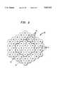
- FIG. 2is a transparent plan view schematic of the layer of thermoelectric elements shown in FIG. 1.
- FIG. 3is a schematic diagram illustrating/he connection of the Peltier elements with a power source.
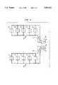
- FIG. 4is a schematic diagram illustrating the coupling of each of the Peltier elements with a corresponding power source.
- the present inventionis shown comprising a reduced-pressure chamber 80 for providing an etching environment and a single wafer support 12 disposed within the chamber 80.
- the chamber 80 of the present inventionis cylindrical in shape. However, it should be understood that the chamber 80 can comprise any shape, such as cubical. Generally, the chamber 80 includes a top surface 88, a bottom surface 86, and a continuous side wall 82. Extending from the top surface 88 of the chamber 80 is an input pipe 100 for supplying an etching gas into the chamber 80. Extending from the side wall 82 of the chamber 80 is an output pipe 102 for removing gas from the chamber. Finally, the side wall 82 of the chamber 80 is connected to ground 89.
- the chamber 80 of the present inventionis fabricated from a conductive metal, such as Aluminum. However, it should be understood that the chamber 80 can be fabricated from any conductive material known in the art capable of maintaining a reduced-pressure environment.
- the support 12comprises a cathode electrode 20, a dielectric isolation layer 30, a layer of thermoelectric elements 40, and chuck means 60.
- the layers of the support 20, 30, 40, 60are designed in size and shape to support the wafer 14.
- each of the layers 20, 30, 40, 60 of the support 12have a diameter of approximately 200 mm, which is the diameter of the wafer 14.
- the size and shape of the layers 20, 30, 40, 60 of the support 12can be varied to accommodate a wafer 14 of any size or shape.
- the cathode electrode 20forms the bottom layer of the support 12 and comprises a top surface 22, a bottom surface 24, and an outer side 23.
- the cathode electrode 20is fabricated from a metal block and provides support for the isolation layer 30, the layer of thermoelectric elements 40, and the chuck means 60.
- the cooling line 25includes the through hole, an input port 26, an output port 27, an input pipe 28, an output pipe 29, and a reservoir 31. It should be understood that the input pipe 28 and output pipe 29 are not restricted to the serpentine configuration shown.
- a coolant 32such as water is contained in the reservoir 31 which is located outside of the chamber 80.
- the coolant 32is pumped (as shown by arrow 33) through the serpentine input pipe 28, which extends into the chamber 80 through an aperture 90 in the bottom surface 86 of the chamber 80, and into the cathode electrode 20 via the input port 26.
- the coolant 32is then circulated through the through-hole to control the temperature associated with the support 12.
- the circulated coolant 32then exits the cathode electrode 20 (as shown by arrow 34) through the serpentine output pipe 29, which extends through an aperture 92 in the bottom surface 86 of the chamber 80 via the output port 27.
- the coolant 32is circulated through the reservoir 31, and the process is repeated.
- the cooling line 25 described hereinis not limited to the configuration shown. Additionally, the coolant 32 can comprise any substance capable of reducing the temperature of the etching tool support 12.
- the cathode electrode 20is capacitively coupled to an RF power source 35 via a coupling capacitor 39 and a match box 37 housing a variable coupling capacitor (not shown).
- a 13.56 MHz power source 35is capacitively coupled to the cathode electrode 20 via a coaxial cable 38 or similar coupling means, which extends from the RF power source 35 through a feed through 96 in the bottom surface 86 of the chamber 80 and to the cathode electrode 20.
- One terminal of the power source 35is connected to ground 36. It should be understood that although a frequency of 13.56 MHz or multiples thereof provides the least amount of interference with radio operations, other frequencies can be employed, depending upon the system parameters.
- the isolation layer 30can be fabricated from any material known in the art for dielectrically isolating the layer of thermoelectric elements 40 from the cathode electrode 20.
- thermoelectric elements 40Disposed above the isolation layer 30 is a layer of thermoelectric elements 40 for locally cooling down or heating up the wafer 14.
- the layer of thermoelectric elements 40can operate under the Peltier Effect (heat is absorbed or generated at the junctions through which an electric current flows) or under the Seebeck Effect (temperature is measured at the junctions through which an electric current flows). It should be understood, however, that the present invention is not limited to the elements described herein.
- FIG. 2fourteen closely packed hexagon shaped Peltier elements 45 (indicated by small bullets) are shown comprising a center area closed loop 53. Similarly, thirty-eight closely packed hexagon shaped Peltier elements 47 (indicated by large bullets) are shown comprising an outer area closed loop 55. The center area dosed loop 53 and the outer area closed loop 55 are isolated via an insulation layer 61.
- the Peltier elements 45, 47are selected and arranged to provide localized temperature control of each region of the wafer 14. However, it should be understood that the number, shape, and size of the Peltier elements 45, 47 can be varied, bearing in mind that localized temperature control is improved by utilizing a greater number of closely packed, smaller Peltier elements.
- the Pettier elements 45, 47 of each closed loop 53, 55are connected in parallel with a first and second DC power source 46, 48, respectively. Specifically, a voltage (V DC1 ) is applied across each of the Peltier elements 45 comprising the center area closed loop 53, and the voltage (V DC2 ) is applied across each of the Peltier elements 47 comprising the outer area closed loop 55.
- first DC power source 46 and the second DC power source 48which are located outside of the chamber 80, to the center area dosed loop 53 and the outer area closed loop 55, via a first pair of feeds 49, 50 and a second pair of feeds 51, 52, respectfully, which extend into the chamber 80 through a feed through 93 in the bottom surface 86 of the chamber 80.
- first pair of feeds 49, 50 and the second pair of feeds 51, 52extend through a first low pass filter 54 and a second low pass filter 56, respectively.
- the multi-loop configuration described hereinprovides superior temperature control as compared to those temperature control devices of the prior art.
- the present inventionis not limited to the center area loop 53 and the outer area loop 55 described herein.
- the number and configuration of the loopscan be varied to address specific temperature control problems encountered during etching, bearing in mind that a greater number of smaller sized loops provides greater localized temperature control.
- the present inventionis not limited to the power supply and feed configurations described herein; the dosed loops can be arranged in any manner for locally controlling the temperature of specific areas of the wafer 14.
- each one of the Peltier elements P 1 -P 52is coupled to a corresponding DC power source V DC1 -V DC52 and a corresponding low pass filter LP 1 -LP 52 to form a closed loop. Accordingly, such a configuration provides greater localized temperature control as compared to those embodiments comprising a fewer number of closed loops.
- a temperature sensing meansDisposed on each of the Peltier elements 45, 47 is a temperature sensing means (not shown), such as a thermocouple, which provides localized temperature sensing at each respective Peltier element 45, 47.
- the temperature sensing meansis not limited to a thermocouple, and can comprise any means for sensing temperature, such as an RTD or a thermistor.
- the chuck means 60Disposed above the layer of Peltier elements 40 is the chuck means 60 for supporting the wafer 14.
- an electrostatic chuck 60of the type that draws and holds the wafer 14 via Coulomb force is provided.
- a conductive layer 62such as Copper, is interposed between a first insulating sheet 64 and a second insulating sheet 66, such as polyimides, to form the electrostatic chuck 60.
- the chuck means 60 of the present inventionis not limited to the electrostatic chuck 60 disclosed herein; any means for supporting the wafer 14 can be utilized, such as a mechanical chuck or a vacuum chuck.
- the electrostatic chuck 60supplies high voltage (V' DC ) to the conductive layer 62 by way of a 2 KV DC power source 68 which is located outside of the chamber 80.
- One terminal of the power source 68is connected to ground 70.
- Poweris fed to the conductive layer 62 through a feed 71 which extends from the power source 68 and through a low pass filter 72 to the conductive layer 62.
- the feed 71extends into the chamber 80 through a feed through 94 in the bottom surface 86 of the chamber 80.
- the power source 68 supplying the chuck 60is not limited to the 2 KV DC source 68 described herein, and can include any power means.
- the wafer 14Upon powering of the chuck 60 via the DC power source 68, the wafer 14 is drawn to the chuck 60 by the electrostatic forces provided. If the surfaces of the wafer 14 are uneven, a plurality of interstices (not shown) may form between the top polyimide layer 64 of the chuck 60 and the wafer 14. These interstices lower the heat exchanging efficiency between the chuck 60 and the wafer 14, which causes the temperature distribution all over the wafer 14 to become non-uniform. In order to reduce these heat exchange losses and to improve the heat transfer characteristics between the wafer 14 and the chuck 60, the interstices can be filled via conventional backfilling techniques, which are well known in the art. Although the backfilling techniques of the present invention use Helium gas, it should be understood that any gas which increases the heat transfer characteristics between the wafer 14 and the chuck 60 can be utilized.
- an etching gassuch as Hydrogen Bromine or Nitrogen Tetrafluoride is introduced into the chamber 80 (as shown by arrow 101) via the input pipe 100, which extends from the top surface 88 of the chamber 80.
- High frequency poweris supplied from the RF power source 35 to between the top surface 88 of the chamber 80, which serves as an upper electrode, and the cathode electrode 20, and a magnetic field is generated therebetween.
- a volume of plasma(not shown) comprising among others ions and free radicals is generated.
- Excess gas and volatile etch productsare then pumped out of the chamber 80 (as shown by arrow 103) through the output pipe 102, which extends from the side wall 82 of the chamber 80, via a vacuum pump (not shown) which is located outside of the chamber 80.
- the Peltier elements 45, 47can be forced to locally cool down or to locally heat up specific areas of the wafer 14 during the etching process.
- a controllercan be provided (not shown) to compare a sensed local temperature with a given setpoint or reference temperature, such as the mean temperature value of all the Peltier elements 45, 47. Upon indication of a temperature that exceeds a predetermined value, any of the closed loops 53, 55 can be energized to cool down or heat up specific areas of the wafer 14.
- each of the Peltier elements 45, 47can function as a temperature sensor by operating under the Seebeck effect (the generation of an electromotive force by a temperature difference between the junctions in a circuit composed of two homogeneous electric conductors of dissimilar composition). By periodically interrupting the current through the Peltier elements 45, 47, the thermovoltage across the Pettier elements 45, 47 can be measured. If a reference temperature is known, such as that of the cooled chuck 60 or that of the temperature measured locally at each thermocouple (not shown), the temperature at each Peltier element 45, 47 can be calculated from the measured thermovoltage. This arrangement provides a simpler construction than that of the arrangement described above, since the number of thermocouples required for reference temperature measurements can be less than the number of Peltier elements 45, 47.
- the present inventionprovides an apparatus for controlling the temperature of a semiconductor wafer during processing.
- the apparatus of the present inventionprovides a layer of thermoelectric elements for locally cooling down or locally heating up a specific area of a wafer surface during etching.
- the present inventionprovides a plurality of closed loops of connected Peltier elements for controlling the temperature of specific areas of a wafer during etching that is more accurate and flexible than those devices of the prior art.
- the apparatus of the present inventionis quicker in response time for controlling the temperature of a wafer as compared to those devices of the prior art.
- the present inventionprovides a plurality of Peltier elements for measuring the temperature profile of a wafer in-situ, which is simpler in construction than those devices of the prior art.
Landscapes
- Engineering & Computer Science (AREA)
- Physics & Mathematics (AREA)
- Condensed Matter Physics & Semiconductors (AREA)
- General Physics & Mathematics (AREA)
- Manufacturing & Machinery (AREA)
- Computer Hardware Design (AREA)
- Microelectronics & Electronic Packaging (AREA)
- Power Engineering (AREA)
- Drying Of Semiconductors (AREA)
- Container, Conveyance, Adherence, Positioning, Of Wafer (AREA)
- Chemical Vapour Deposition (AREA)
Abstract
Description
Claims (20)
Priority Applications (7)
| Application Number | Priority Date | Filing Date | Title |
|---|---|---|---|
| US08/519,373US5667622A (en) | 1995-08-25 | 1995-08-25 | In-situ wafer temperature control apparatus for single wafer tools |
| EP96112921AEP0762480B1 (en) | 1995-08-25 | 1996-08-09 | Single wafer tool comprising an in-situ wafer temperature control apparatus |
| DE69630501TDE69630501T2 (en) | 1995-08-25 | 1996-08-09 | Device for processing single semiconductor wafers with in-situ temperature control |
| CN96113324ACN1088258C (en) | 1995-08-25 | 1996-08-25 | Crystal wafer temmperature on-site controller for single wafer tool |
| KR1019960035495AKR100395846B1 (en) | 1995-08-25 | 1996-08-26 | In-situ wafer temperature controller for single wafer tool |
| JP22415596AJPH09205080A (en) | 1995-08-25 | 1996-08-26 | Wafer temperature controller for single wafer equipment |
| TW085110969ATW494588B (en) | 1995-08-25 | 1996-09-07 | A temperature control apparatus for single wafer etching tool |
Applications Claiming Priority (1)
| Application Number | Priority Date | Filing Date | Title |
|---|---|---|---|
| US08/519,373US5667622A (en) | 1995-08-25 | 1995-08-25 | In-situ wafer temperature control apparatus for single wafer tools |
Publications (1)
| Publication Number | Publication Date |
|---|---|
| US5667622Atrue US5667622A (en) | 1997-09-16 |
Family
ID=24068032
Family Applications (1)
| Application Number | Title | Priority Date | Filing Date |
|---|---|---|---|
| US08/519,373Expired - LifetimeUS5667622A (en) | 1995-08-25 | 1995-08-25 | In-situ wafer temperature control apparatus for single wafer tools |
Country Status (7)
| Country | Link |
|---|---|
| US (1) | US5667622A (en) |
| EP (1) | EP0762480B1 (en) |
| JP (1) | JPH09205080A (en) |
| KR (1) | KR100395846B1 (en) |
| CN (1) | CN1088258C (en) |
| DE (1) | DE69630501T2 (en) |
| TW (1) | TW494588B (en) |
Cited By (60)
| Publication number | Priority date | Publication date | Assignee | Title |
|---|---|---|---|---|
| US5901030A (en)* | 1997-12-02 | 1999-05-04 | Dorsey Gage, Inc. | Electrostatic chuck employing thermoelectric cooling |
| US5996353A (en)* | 1998-05-21 | 1999-12-07 | Applied Materials, Inc. | Semiconductor processing system with a thermoelectric cooling/heating device |
| US6214121B1 (en)* | 1999-07-07 | 2001-04-10 | Applied Materials, Inc. | Pedestal with a thermally controlled platen |
| US6278600B1 (en) | 1994-01-31 | 2001-08-21 | Applied Materials, Inc. | Electrostatic chuck with improved temperature control and puncture resistance |
| US6320736B1 (en) | 1999-05-17 | 2001-11-20 | Applied Materials, Inc. | Chuck having pressurized zones of heat transfer gas |
| US6508062B2 (en) | 2001-01-31 | 2003-01-21 | Applied Materials, Inc. | Thermal exchanger for a wafer chuck |
| US20040195207A1 (en)* | 2003-04-03 | 2004-10-07 | Renesas Technology Corp. | Substrate cleaning device and a method for manufacturing electronic devices |
| US20050057184A1 (en)* | 2003-08-25 | 2005-03-17 | Tdk Corporation | Method and apparatus for managing temperature of light emitting element, and lighting apparatus |
| KR100490894B1 (en)* | 1998-02-04 | 2005-08-31 | 삼성전자주식회사 | Wafer Fixed Electrostatic Chuck |
| KR100551890B1 (en) | 2004-12-29 | 2006-02-14 | 동부아남반도체 주식회사 | Helium temperature controller for wafer temperature control |
| US7297894B1 (en) | 2006-09-25 | 2007-11-20 | Tokyo Electron Limited | Method for multi-step temperature control of a substrate |
| US20070283709A1 (en)* | 2006-06-09 | 2007-12-13 | Veeco Instruments Inc. | Apparatus and methods for managing the temperature of a substrate in a high vacuum processing system |
| US20080017104A1 (en)* | 2006-07-20 | 2008-01-24 | Applied Materials, Inc. | Substrate processing with rapid temperature gradient control |
| US20080083738A1 (en)* | 2006-09-25 | 2008-04-10 | Tokyo Electron Limited | High rate method for stable temperature control of a substrate |
| US20080083724A1 (en)* | 2006-09-25 | 2008-04-10 | Tokyo Electron Limited | Temperature controlled substrate holder having erosion resistant insulating layer for a substrate processing system |
| US20080083723A1 (en)* | 2006-09-25 | 2008-04-10 | Tokyo Electron Limited | Temperature controlled substrate holder with non-uniform insulation layer for a substrate processing system |
| US20080230377A1 (en)* | 2007-03-19 | 2008-09-25 | Micron Technology, Inc. | Apparatus and methods for capacitively coupled plasma vapor processing of semiconductor wafers |
| US20110092072A1 (en)* | 2009-10-21 | 2011-04-21 | Lam Research Corporation | Heating plate with planar heating zones for semiconductor processing |
| US20110143462A1 (en)* | 2009-12-15 | 2011-06-16 | Lam Research Corporation | Adjusting substrate temperature to improve cd uniformity |
| US8222511B2 (en) | 2006-08-03 | 2012-07-17 | Gentherm | Thermoelectric device |
| US8226769B2 (en) | 2006-04-27 | 2012-07-24 | Applied Materials, Inc. | Substrate support with electrostatic chuck having dual temperature zones |
| US20130045883A1 (en)* | 2002-07-30 | 2013-02-21 | Life Technologies Corporation | Sample Block Apparatus and Method for Maintaining a Microcard on a Sample Block |
| US8461674B2 (en) | 2011-09-21 | 2013-06-11 | Lam Research Corporation | Thermal plate with planar thermal zones for semiconductor processing |
| US20130145615A1 (en)* | 2011-12-07 | 2013-06-13 | International Business Machines Corporation | Detecting Leaks In A Fluid Cooling System By Sensing For A Drop Of Fluid Pressure In The System |
| US8546732B2 (en) | 2010-11-10 | 2013-10-01 | Lam Research Corporation | Heating plate with planar heater zones for semiconductor processing |
| US8558193B2 (en) | 2009-07-08 | 2013-10-15 | Hitachi High-Technologies Corporation | Charged particle beam device |
| US8624168B2 (en) | 2011-09-20 | 2014-01-07 | Lam Research Corporation | Heating plate with diode planar heater zones for semiconductor processing |
| US8791392B2 (en) | 2010-10-22 | 2014-07-29 | Lam Research Corporation | Methods of fault detection for multiplexed heater array |
| US8809747B2 (en) | 2012-04-13 | 2014-08-19 | Lam Research Corporation | Current peak spreading schemes for multiplexed heated array |
| US20150288302A1 (en)* | 2012-11-27 | 2015-10-08 | Creative Technology Corporation | Electrostatic chuck, glass substrate processing method, and said glass substrate |
| US9307578B2 (en) | 2011-08-17 | 2016-04-05 | Lam Research Corporation | System and method for monitoring temperatures of and controlling multiplexed heater array |
| US9324589B2 (en) | 2012-02-28 | 2016-04-26 | Lam Research Corporation | Multiplexed heater array using AC drive for semiconductor processing |
| US20160370796A1 (en)* | 2015-06-22 | 2016-12-22 | Lam Research Corporation | System and method for determining field non-uniformities of a wafer processing chamber using a wafer processing parameter |
| US9622588B2 (en) | 2008-07-18 | 2017-04-18 | Gentherm Incorporated | Environmentally-conditioned bed |
| US9651279B2 (en) | 2008-02-01 | 2017-05-16 | Gentherm Incorporated | Condensation and humidity sensors for thermoelectric devices |
| US9662962B2 (en) | 2013-11-05 | 2017-05-30 | Gentherm Incorporated | Vehicle headliner assembly for zonal comfort |
| US9685599B2 (en) | 2011-10-07 | 2017-06-20 | Gentherm Incorporated | Method and system for controlling an operation of a thermoelectric device |
| US20170178978A1 (en)* | 2015-12-18 | 2017-06-22 | Samsung Electronics Co., Ltd. | Electrostatic chuck assembly, semiconductor manufacturing apparatus having the same, and method of measuring temperature of electrostatic chuck |
| US9748120B2 (en) | 2013-07-01 | 2017-08-29 | Lam Research Ag | Apparatus for liquid treatment of disc-shaped articles and heating system for use in such apparatus |
| US9857107B2 (en) | 2006-10-12 | 2018-01-02 | Gentherm Incorporated | Thermoelectric device with internal sensor |
| US9989267B2 (en) | 2012-02-10 | 2018-06-05 | Gentherm Incorporated | Moisture abatement in heating operation of climate controlled systems |
| US10005337B2 (en) | 2004-12-20 | 2018-06-26 | Gentherm Incorporated | Heating and cooling systems for seating assemblies |
| US10026634B2 (en) | 2014-10-22 | 2018-07-17 | Shinko Electric Industries Co., Ltd. | Electrostatic chuck and base member for use in the same |
| US10049948B2 (en) | 2012-11-30 | 2018-08-14 | Lam Research Corporation | Power switching system for ESC with array of thermal control elements |
| US10096506B2 (en) | 2015-06-22 | 2018-10-09 | Lam Research Corporation | Reducing temperature transition in a substrate support |
| US10325798B2 (en) | 2010-12-20 | 2019-06-18 | Ev Group E. Thallner Gmbh | Accommodating device for retaining wafers |
| US10381248B2 (en) | 2015-06-22 | 2019-08-13 | Lam Research Corporation | Auto-correction of electrostatic chuck temperature non-uniformity |
| US10388493B2 (en) | 2011-09-16 | 2019-08-20 | Lam Research Corporation | Component of a substrate support assembly producing localized magnetic fields |
| US10386821B2 (en) | 2015-06-22 | 2019-08-20 | Lam Research Corporation | Systems and methods for calibrating scalar field contribution values for a limited number of sensors including a temperature value of an electrostatic chuck and estimating temperature distribution profiles based on calibrated values |
| US10405667B2 (en) | 2007-09-10 | 2019-09-10 | Gentherm Incorporated | Climate controlled beds and methods of operating the same |
| US10490426B2 (en) | 2014-08-26 | 2019-11-26 | Lam Research Ag | Method and apparatus for processing wafer-shaped articles |
| US10991869B2 (en) | 2018-07-30 | 2021-04-27 | Gentherm Incorporated | Thermoelectric device having a plurality of sealing materials |
| US11033058B2 (en) | 2014-11-14 | 2021-06-15 | Gentherm Incorporated | Heating and cooling technologies |
| US11152557B2 (en) | 2019-02-20 | 2021-10-19 | Gentherm Incorporated | Thermoelectric module with integrated printed circuit board |
| US11164759B2 (en) | 2018-05-10 | 2021-11-02 | Micron Technology, Inc. | Tools and systems for processing one or more semiconductor devices, and related methods |
| US11240883B2 (en) | 2014-02-14 | 2022-02-01 | Gentherm Incorporated | Conductive convective climate controlled seat |
| CN114269969A (en)* | 2019-06-24 | 2022-04-01 | 朗姆研究公司 | Temperature control of multi-segment bases |
| US11639816B2 (en) | 2014-11-14 | 2023-05-02 | Gentherm Incorporated | Heating and cooling technologies including temperature regulating pad wrap and technologies with liquid system |
| US11857004B2 (en) | 2014-11-14 | 2024-01-02 | Gentherm Incorporated | Heating and cooling technologies |
| US11993132B2 (en) | 2018-11-30 | 2024-05-28 | Gentherm Incorporated | Thermoelectric conditioning system and methods |
Families Citing this family (14)
| Publication number | Priority date | Publication date | Assignee | Title |
|---|---|---|---|---|
| US5983644A (en)* | 1997-09-29 | 1999-11-16 | Applied Materials, Inc. | Integrated bake and chill plate |
| US6271459B1 (en)* | 2000-04-26 | 2001-08-07 | Wafermasters, Inc. | Heat management in wafer processing equipment using thermoelectric device |
| US6643604B1 (en) | 2000-06-30 | 2003-11-04 | Advanced Micro Devices, Inc. | System for uniformly heating photoresist |
| TWI303084B (en)* | 2000-09-08 | 2008-11-11 | Tokyo Electron Ltd | Shower head structure, film forming method, and gas processing apparauts |
| KR100420226B1 (en)* | 2001-06-28 | 2004-03-04 | 동부전자 주식회사 | Electrostatic chuck for a plasma process apparatus |
| US6745575B2 (en) | 2002-07-11 | 2004-06-08 | Temptronic Corporation | Workpiece chuck with temperature control assembly having spacers between layers providing clearance for thermoelectric modules |
| JP4403073B2 (en) | 2002-07-11 | 2010-01-20 | テンプトロニック コーポレイション | Workpiece chuck with thermal control assembly having interlayer spacers to create gaps for thermoelectric modules |
| JP4442171B2 (en) | 2003-09-24 | 2010-03-31 | 東京エレクトロン株式会社 | Heat treatment equipment |
| JP2005302851A (en)* | 2004-04-08 | 2005-10-27 | Tokyo Electron Ltd | Substrate mounting table and heat treatment apparatus |
| US7378618B1 (en)* | 2006-12-14 | 2008-05-27 | Applied Materials, Inc. | Rapid conductive cooling using a secondary process plane |
| JP5131762B2 (en)* | 2008-05-09 | 2013-01-30 | サムコ株式会社 | Plasma processing method, plasma processing apparatus, and plasma processing tray |
| US9706605B2 (en)* | 2012-03-30 | 2017-07-11 | Applied Materials, Inc. | Substrate support with feedthrough structure |
| JP6863041B2 (en)* | 2017-04-21 | 2021-04-21 | 東京エレクトロン株式会社 | Substrate heating device |
| CN118866759B (en)* | 2024-07-08 | 2025-02-18 | 安徽华迅科技有限公司 | Chip fixing device for chip processing equipment |
Citations (4)
| Publication number | Priority date | Publication date | Assignee | Title |
|---|---|---|---|---|
| US4493939A (en)* | 1983-10-31 | 1985-01-15 | Varo, Inc. | Method and apparatus for fabricating a thermoelectric array |
| US5179333A (en)* | 1989-11-17 | 1993-01-12 | Kabushiki Kaisha Toshiba | Apparatus for measuring the electrical characteristics of a semiconductor wafer |
| US5270266A (en)* | 1991-12-13 | 1993-12-14 | Tokyo Electron Limited | Method of adjusting the temperature of a semiconductor wafer |
| US5374888A (en)* | 1991-09-05 | 1994-12-20 | Tokyo Electron Kabushiki Kaisha | Electrical characteristics measurement method and measurement apparatus therefor |
Family Cites Families (3)
| Publication number | Priority date | Publication date | Assignee | Title |
|---|---|---|---|---|
| JPH01152639A (en)* | 1987-12-10 | 1989-06-15 | Canon Inc | Chuck |
| JP2737010B2 (en)* | 1989-08-01 | 1998-04-08 | キヤノン株式会社 | Exposure equipment |
| US5059770A (en)* | 1989-09-19 | 1991-10-22 | Watkins-Johnson Company | Multi-zone planar heater assembly and method of operation |
- 1995
- 1995-08-25USUS08/519,373patent/US5667622A/ennot_activeExpired - Lifetime
- 1996
- 1996-08-09EPEP96112921Apatent/EP0762480B1/ennot_activeExpired - Lifetime
- 1996-08-09DEDE69630501Tpatent/DE69630501T2/ennot_activeExpired - Fee Related
- 1996-08-25CNCN96113324Apatent/CN1088258C/ennot_activeExpired - Fee Related
- 1996-08-26JPJP22415596Apatent/JPH09205080A/enactivePending
- 1996-08-26KRKR1019960035495Apatent/KR100395846B1/ennot_activeExpired - Fee Related
- 1996-09-07TWTW085110969Apatent/TW494588B/ennot_activeIP Right Cessation
Patent Citations (4)
| Publication number | Priority date | Publication date | Assignee | Title |
|---|---|---|---|---|
| US4493939A (en)* | 1983-10-31 | 1985-01-15 | Varo, Inc. | Method and apparatus for fabricating a thermoelectric array |
| US5179333A (en)* | 1989-11-17 | 1993-01-12 | Kabushiki Kaisha Toshiba | Apparatus for measuring the electrical characteristics of a semiconductor wafer |
| US5374888A (en)* | 1991-09-05 | 1994-12-20 | Tokyo Electron Kabushiki Kaisha | Electrical characteristics measurement method and measurement apparatus therefor |
| US5270266A (en)* | 1991-12-13 | 1993-12-14 | Tokyo Electron Limited | Method of adjusting the temperature of a semiconductor wafer |
Cited By (119)
| Publication number | Priority date | Publication date | Assignee | Title |
|---|---|---|---|---|
| US6278600B1 (en) | 1994-01-31 | 2001-08-21 | Applied Materials, Inc. | Electrostatic chuck with improved temperature control and puncture resistance |
| WO1999028950A3 (en)* | 1997-12-02 | 1999-08-05 | Dorsey Gage Inc | Electrostatic chuck employing thermoelectric cooling |
| US5901030A (en)* | 1997-12-02 | 1999-05-04 | Dorsey Gage, Inc. | Electrostatic chuck employing thermoelectric cooling |
| KR100490894B1 (en)* | 1998-02-04 | 2005-08-31 | 삼성전자주식회사 | Wafer Fixed Electrostatic Chuck |
| US5996353A (en)* | 1998-05-21 | 1999-12-07 | Applied Materials, Inc. | Semiconductor processing system with a thermoelectric cooling/heating device |
| US6320736B1 (en) | 1999-05-17 | 2001-11-20 | Applied Materials, Inc. | Chuck having pressurized zones of heat transfer gas |
| US6656286B2 (en) | 1999-07-07 | 2003-12-02 | Applied Materials, Inc. | Pedestal with a thermally controlled platen |
| US6214121B1 (en)* | 1999-07-07 | 2001-04-10 | Applied Materials, Inc. | Pedestal with a thermally controlled platen |
| US6508062B2 (en) | 2001-01-31 | 2003-01-21 | Applied Materials, Inc. | Thermal exchanger for a wafer chuck |
| US10253361B2 (en) | 2002-07-30 | 2019-04-09 | Applied Biosystems, Llc | Sample block apparatus and method for maintaining a microcard on a sample block |
| US20130045883A1 (en)* | 2002-07-30 | 2013-02-21 | Life Technologies Corporation | Sample Block Apparatus and Method for Maintaining a Microcard on a Sample Block |
| US20040195207A1 (en)* | 2003-04-03 | 2004-10-07 | Renesas Technology Corp. | Substrate cleaning device and a method for manufacturing electronic devices |
| US20050057184A1 (en)* | 2003-08-25 | 2005-03-17 | Tdk Corporation | Method and apparatus for managing temperature of light emitting element, and lighting apparatus |
| US10005337B2 (en) | 2004-12-20 | 2018-06-26 | Gentherm Incorporated | Heating and cooling systems for seating assemblies |
| KR100551890B1 (en) | 2004-12-29 | 2006-02-14 | 동부아남반도체 주식회사 | Helium temperature controller for wafer temperature control |
| US8226769B2 (en) | 2006-04-27 | 2012-07-24 | Applied Materials, Inc. | Substrate support with electrostatic chuck having dual temperature zones |
| US8663391B2 (en) | 2006-04-27 | 2014-03-04 | Applied Materials, Inc. | Electrostatic chuck having a plurality of heater coils |
| US20070283709A1 (en)* | 2006-06-09 | 2007-12-13 | Veeco Instruments Inc. | Apparatus and methods for managing the temperature of a substrate in a high vacuum processing system |
| US9275887B2 (en) | 2006-07-20 | 2016-03-01 | Applied Materials, Inc. | Substrate processing with rapid temperature gradient control |
| US10257887B2 (en) | 2006-07-20 | 2019-04-09 | Applied Materials, Inc. | Substrate support assembly |
| US9883549B2 (en) | 2006-07-20 | 2018-01-30 | Applied Materials, Inc. | Substrate support assembly having rapid temperature control |
| US20080017104A1 (en)* | 2006-07-20 | 2008-01-24 | Applied Materials, Inc. | Substrate processing with rapid temperature gradient control |
| US8222511B2 (en) | 2006-08-03 | 2012-07-17 | Gentherm | Thermoelectric device |
| US7893387B2 (en) | 2006-09-25 | 2011-02-22 | Tokyo Electron Limited | High rate method for stable temperature control of a substrate |
| US20080083724A1 (en)* | 2006-09-25 | 2008-04-10 | Tokyo Electron Limited | Temperature controlled substrate holder having erosion resistant insulating layer for a substrate processing system |
| US20110015803A1 (en)* | 2006-09-25 | 2011-01-20 | Tokyo Electron Limited | High rate method for stable temperature control of a substrate |
| US7838800B2 (en) | 2006-09-25 | 2010-11-23 | Tokyo Electron Limited | Temperature controlled substrate holder having erosion resistant insulating layer for a substrate processing system |
| US7297894B1 (en) | 2006-09-25 | 2007-11-20 | Tokyo Electron Limited | Method for multi-step temperature control of a substrate |
| US7952049B2 (en) | 2006-09-25 | 2011-05-31 | Tokyo Electron Limited | Method for multi-step temperature control of a substrate |
| US20080083738A1 (en)* | 2006-09-25 | 2008-04-10 | Tokyo Electron Limited | High rate method for stable temperature control of a substrate |
| US8084720B2 (en) | 2006-09-25 | 2011-12-27 | Tokyo Electron Limited | High rate method for stable temperature control of a substrate |
| US8207476B2 (en) | 2006-09-25 | 2012-06-26 | Tokyo Electron Limited | Temperature controlled substrate holder with non-uniform insulation layer for a substrate processing system |
| US7723648B2 (en) | 2006-09-25 | 2010-05-25 | Tokyo Electron Limited | Temperature controlled substrate holder with non-uniform insulation layer for a substrate processing system |
| US20100078424A1 (en)* | 2006-09-25 | 2010-04-01 | Tokyo Electron Limited | Temperature controlled substrate holder with non-uniform insulation layer for a substrate processing system |
| US20110011845A1 (en)* | 2006-09-25 | 2011-01-20 | Tokyo Electron Limited | Temperature controlled substrate holder having erosion resistant insulating layer for a substrate processing system |
| US20090266809A1 (en)* | 2006-09-25 | 2009-10-29 | Tokyo Electron Limited | High rate method for stable temperature control of a substrate |
| US8450657B2 (en) | 2006-09-25 | 2013-05-28 | Tokyo Electron Limited | Temperature controlled substrate holder having erosion resistant insulating layer for a substrate processing system |
| US20080083723A1 (en)* | 2006-09-25 | 2008-04-10 | Tokyo Electron Limited | Temperature controlled substrate holder with non-uniform insulation layer for a substrate processing system |
| US7557328B2 (en) | 2006-09-25 | 2009-07-07 | Tokyo Electron Limited | High rate method for stable temperature control of a substrate |
| US9857107B2 (en) | 2006-10-12 | 2018-01-02 | Gentherm Incorporated | Thermoelectric device with internal sensor |
| US8375890B2 (en)* | 2007-03-19 | 2013-02-19 | Micron Technology, Inc. | Apparatus and methods for capacitively coupled plasma vapor processing of semiconductor wafers |
| US8910591B2 (en) | 2007-03-19 | 2014-12-16 | Micron Technology, Inc. | Apparatus and methods for capacitively coupled plasma vapor processing of semiconductor wafers |
| US20080230377A1 (en)* | 2007-03-19 | 2008-09-25 | Micron Technology, Inc. | Apparatus and methods for capacitively coupled plasma vapor processing of semiconductor wafers |
| US10405667B2 (en) | 2007-09-10 | 2019-09-10 | Gentherm Incorporated | Climate controlled beds and methods of operating the same |
| US9651279B2 (en) | 2008-02-01 | 2017-05-16 | Gentherm Incorporated | Condensation and humidity sensors for thermoelectric devices |
| US10228166B2 (en) | 2008-02-01 | 2019-03-12 | Gentherm Incorporated | Condensation and humidity sensors for thermoelectric devices |
| US11297953B2 (en) | 2008-07-18 | 2022-04-12 | Sleep Number Corporation | Environmentally-conditioned bed |
| US12016466B2 (en) | 2008-07-18 | 2024-06-25 | Sleep Number Corporation | Environmentally-conditioned mattress |
| US10226134B2 (en) | 2008-07-18 | 2019-03-12 | Gentherm Incorporated | Environmentally-conditioned bed |
| US12274365B2 (en) | 2008-07-18 | 2025-04-15 | Sleep Number Corporation | Climate controlled bed with fluid distribution member |
| US9622588B2 (en) | 2008-07-18 | 2017-04-18 | Gentherm Incorporated | Environmentally-conditioned bed |
| US8558193B2 (en) | 2009-07-08 | 2013-10-15 | Hitachi High-Technologies Corporation | Charged particle beam device |
| US9646861B2 (en) | 2009-10-21 | 2017-05-09 | Lam Research Corporation | Heating plate with heating zones for substrate processing and method of use thereof |
| US10236193B2 (en) | 2009-10-21 | 2019-03-19 | Lam Research Corporation | Substrate supports with multi-layer structure including independent operated heater zones |
| US8637794B2 (en) | 2009-10-21 | 2014-01-28 | Lam Research Corporation | Heating plate with planar heating zones for semiconductor processing |
| US10720346B2 (en) | 2009-10-21 | 2020-07-21 | Lam Research Corporation | Substrate support with thermal zones for semiconductor processing |
| US9392643B2 (en) | 2009-10-21 | 2016-07-12 | Lam Research Corporation | Heating plate with planar heater zones for semiconductor processing |
| US20110092072A1 (en)* | 2009-10-21 | 2011-04-21 | Lam Research Corporation | Heating plate with planar heating zones for semiconductor processing |
| US8884194B2 (en) | 2009-10-21 | 2014-11-11 | Lam Research Corporation | Heating plate with planar heater zones for semiconductor processing |
| US20110143462A1 (en)* | 2009-12-15 | 2011-06-16 | Lam Research Corporation | Adjusting substrate temperature to improve cd uniformity |
| US8642480B2 (en) | 2009-12-15 | 2014-02-04 | Lam Research Corporation | Adjusting substrate temperature to improve CD uniformity |
| US10056225B2 (en) | 2009-12-15 | 2018-08-21 | Lam Research Corporation | Adjusting substrate temperature to improve CD uniformity |
| US8791392B2 (en) | 2010-10-22 | 2014-07-29 | Lam Research Corporation | Methods of fault detection for multiplexed heater array |
| US10568163B2 (en) | 2010-10-22 | 2020-02-18 | Lam Research Corporation | Methods of fault detection for multiplexed heater array |
| US8680441B2 (en) | 2010-11-10 | 2014-03-25 | Lam Research Corporation | Heating plate with planar heater zones for semiconductor processing |
| US8546732B2 (en) | 2010-11-10 | 2013-10-01 | Lam Research Corporation | Heating plate with planar heater zones for semiconductor processing |
| US11756818B2 (en) | 2010-12-20 | 2023-09-12 | Ev Group E. Thallner Gmbh | Accommodating device for retaining wafers |
| US11355374B2 (en) | 2010-12-20 | 2022-06-07 | Ev Group E. Thallner Gmbh | Accommodating device for retaining wafers |
| US10325798B2 (en) | 2010-12-20 | 2019-06-18 | Ev Group E. Thallner Gmbh | Accommodating device for retaining wafers |
| US10886156B2 (en) | 2010-12-20 | 2021-01-05 | Ev Group E. Thallner Gmbh | Accomodating device for retaining wafers |
| US9713200B2 (en) | 2011-08-17 | 2017-07-18 | Lam Research Corporation | System and method for monitoring temperatures of and controlling multiplexed heater array |
| US9307578B2 (en) | 2011-08-17 | 2016-04-05 | Lam Research Corporation | System and method for monitoring temperatures of and controlling multiplexed heater array |
| US10872748B2 (en) | 2011-09-16 | 2020-12-22 | Lam Research Corporation | Systems and methods for correcting non-uniformities in plasma processing of substrates |
| US10388493B2 (en) | 2011-09-16 | 2019-08-20 | Lam Research Corporation | Component of a substrate support assembly producing localized magnetic fields |
| US8624168B2 (en) | 2011-09-20 | 2014-01-07 | Lam Research Corporation | Heating plate with diode planar heater zones for semiconductor processing |
| US8461674B2 (en) | 2011-09-21 | 2013-06-11 | Lam Research Corporation | Thermal plate with planar thermal zones for semiconductor processing |
| US8587113B2 (en) | 2011-09-21 | 2013-11-19 | Lam Research Corporation | Thermal plate with planar thermal zones for semiconductor processing |
| US9685599B2 (en) | 2011-10-07 | 2017-06-20 | Gentherm Incorporated | Method and system for controlling an operation of a thermoelectric device |
| US10208990B2 (en) | 2011-10-07 | 2019-02-19 | Gentherm Incorporated | Thermoelectric device controls and methods |
| US8763445B2 (en)* | 2011-12-07 | 2014-07-01 | International Business Machines Corporation | Detecting leaks in a fluid cooling system by sensing for a drop of fluid pressure in the system |
| US20130145615A1 (en)* | 2011-12-07 | 2013-06-13 | International Business Machines Corporation | Detecting Leaks In A Fluid Cooling System By Sensing For A Drop Of Fluid Pressure In The System |
| US10495322B2 (en) | 2012-02-10 | 2019-12-03 | Gentherm Incorporated | Moisture abatement in heating operation of climate controlled systems |
| US9989267B2 (en) | 2012-02-10 | 2018-06-05 | Gentherm Incorporated | Moisture abatement in heating operation of climate controlled systems |
| US9775194B2 (en) | 2012-02-28 | 2017-09-26 | Lam Research Corporation | Multiplexed heater array using AC drive for semiconductor processing |
| US9324589B2 (en) | 2012-02-28 | 2016-04-26 | Lam Research Corporation | Multiplexed heater array using AC drive for semiconductor processing |
| US8809747B2 (en) | 2012-04-13 | 2014-08-19 | Lam Research Corporation | Current peak spreading schemes for multiplexed heated array |
| US9866151B2 (en)* | 2012-11-27 | 2018-01-09 | Creative Technology Corporation | Electrostatic chuck, glass substrate processing method, and said glass substrate |
| US20150288302A1 (en)* | 2012-11-27 | 2015-10-08 | Creative Technology Corporation | Electrostatic chuck, glass substrate processing method, and said glass substrate |
| US10049948B2 (en) | 2012-11-30 | 2018-08-14 | Lam Research Corporation | Power switching system for ESC with array of thermal control elements |
| US10770363B2 (en) | 2012-11-30 | 2020-09-08 | Lam Research Corporation | Power switching system for ESC with array of thermal control elements |
| US9748120B2 (en) | 2013-07-01 | 2017-08-29 | Lam Research Ag | Apparatus for liquid treatment of disc-shaped articles and heating system for use in such apparatus |
| US10266031B2 (en) | 2013-11-05 | 2019-04-23 | Gentherm Incorporated | Vehicle headliner assembly for zonal comfort |
| US9662962B2 (en) | 2013-11-05 | 2017-05-30 | Gentherm Incorporated | Vehicle headliner assembly for zonal comfort |
| US11240883B2 (en) | 2014-02-14 | 2022-02-01 | Gentherm Incorporated | Conductive convective climate controlled seat |
| US11240882B2 (en) | 2014-02-14 | 2022-02-01 | Gentherm Incorporated | Conductive convective climate controlled seat |
| US10490426B2 (en) | 2014-08-26 | 2019-11-26 | Lam Research Ag | Method and apparatus for processing wafer-shaped articles |
| US11195730B2 (en) | 2014-08-26 | 2021-12-07 | Lam Research Ag | Method and apparatus for processing wafer-shaped articles |
| US10026634B2 (en) | 2014-10-22 | 2018-07-17 | Shinko Electric Industries Co., Ltd. | Electrostatic chuck and base member for use in the same |
| US11639816B2 (en) | 2014-11-14 | 2023-05-02 | Gentherm Incorporated | Heating and cooling technologies including temperature regulating pad wrap and technologies with liquid system |
| US11857004B2 (en) | 2014-11-14 | 2024-01-02 | Gentherm Incorporated | Heating and cooling technologies |
| US11033058B2 (en) | 2014-11-14 | 2021-06-15 | Gentherm Incorporated | Heating and cooling technologies |
| US10381248B2 (en) | 2015-06-22 | 2019-08-13 | Lam Research Corporation | Auto-correction of electrostatic chuck temperature non-uniformity |
| US11029668B2 (en) | 2015-06-22 | 2021-06-08 | Lam Research Corporation | Systems and methods for calibrating scalar field contribution values for a limited number of sensors including a temperature value of an electrostatic chuck and estimating temperature distribution profiles based on calibrated values |
| US20160370796A1 (en)* | 2015-06-22 | 2016-12-22 | Lam Research Corporation | System and method for determining field non-uniformities of a wafer processing chamber using a wafer processing parameter |
| US10096506B2 (en) | 2015-06-22 | 2018-10-09 | Lam Research Corporation | Reducing temperature transition in a substrate support |
| US10763142B2 (en)* | 2015-06-22 | 2020-09-01 | Lam Research Corporation | System and method for determining field non-uniformities of a wafer processing chamber using a wafer processing parameter |
| US10386821B2 (en) | 2015-06-22 | 2019-08-20 | Lam Research Corporation | Systems and methods for calibrating scalar field contribution values for a limited number of sensors including a temperature value of an electrostatic chuck and estimating temperature distribution profiles based on calibrated values |
| KR20170073352A (en)* | 2015-12-18 | 2017-06-28 | 삼성전자주식회사 | A electrostatic chuck assembly, a semiconductor manufacturing apparatus having the same, and a temperature mesuring method for electrostatic chuck |
| US9812372B2 (en)* | 2015-12-18 | 2017-11-07 | Samsung Electronics Co., Ltd. | Electrostatic chuck assembly, semiconductor manufacturing apparatus having the same, and method of measuring temperature of electrostatic chuck |
| US20170178978A1 (en)* | 2015-12-18 | 2017-06-22 | Samsung Electronics Co., Ltd. | Electrostatic chuck assembly, semiconductor manufacturing apparatus having the same, and method of measuring temperature of electrostatic chuck |
| US11164759B2 (en) | 2018-05-10 | 2021-11-02 | Micron Technology, Inc. | Tools and systems for processing one or more semiconductor devices, and related methods |
| US12020955B2 (en) | 2018-05-10 | 2024-06-25 | Micron Technology, Inc. | Systems for processing one or more semiconductor devices, and related methods |
| US11223004B2 (en) | 2018-07-30 | 2022-01-11 | Gentherm Incorporated | Thermoelectric device having a polymeric coating |
| US11075331B2 (en) | 2018-07-30 | 2021-07-27 | Gentherm Incorporated | Thermoelectric device having circuitry with structural rigidity |
| US10991869B2 (en) | 2018-07-30 | 2021-04-27 | Gentherm Incorporated | Thermoelectric device having a plurality of sealing materials |
| US11993132B2 (en) | 2018-11-30 | 2024-05-28 | Gentherm Incorporated | Thermoelectric conditioning system and methods |
| US11152557B2 (en) | 2019-02-20 | 2021-10-19 | Gentherm Incorporated | Thermoelectric module with integrated printed circuit board |
| CN114269969A (en)* | 2019-06-24 | 2022-04-01 | 朗姆研究公司 | Temperature control of multi-segment bases |
| US12209312B2 (en) | 2019-06-24 | 2025-01-28 | Lam Research Corporation | Temperature control of a multi-zone pedestal |
Also Published As
| Publication number | Publication date |
|---|---|
| EP0762480B1 (en) | 2003-10-29 |
| JPH09205080A (en) | 1997-08-05 |
| TW494588B (en) | 2002-07-11 |
| CN1088258C (en) | 2002-07-24 |
| DE69630501T2 (en) | 2004-08-05 |
| DE69630501D1 (en) | 2003-12-04 |
| KR100395846B1 (en) | 2003-11-20 |
| KR970013072A (en) | 1997-03-29 |
| EP0762480A1 (en) | 1997-03-12 |
| CN1149761A (en) | 1997-05-14 |
Similar Documents
| Publication | Publication Date | Title |
|---|---|---|
| US5667622A (en) | In-situ wafer temperature control apparatus for single wafer tools | |
| EP0890185B1 (en) | Solid state temperature controlled substrate holder | |
| EP1073096B1 (en) | Semiconductor workpiece processing apparatus | |
| EP1075015A2 (en) | A method and apparatus for thermal control of a semiconductor substrate | |
| KR101840231B1 (en) | Plasma processing apparatus | |
| KR100283853B1 (en) | Plasma process apparatus | |
| US7244311B2 (en) | Heat transfer system for improved semiconductor processing uniformity | |
| KR100904361B1 (en) | Method and system for temperature control of a substrate | |
| TWI494028B (en) | Workpiece support for a plasma reactor with controlled apportionment of rf power to a process kit ring | |
| US8809747B2 (en) | Current peak spreading schemes for multiplexed heated array | |
| US7993460B2 (en) | Substrate support having dynamic temperature control | |
| US20060291132A1 (en) | Electrostatic chuck, wafer processing apparatus and plasma processing method | |
| US20120070914A1 (en) | Temperature control module using gas pressure to control thermal conductance between liquid coolant and component body | |
| US20030087488A1 (en) | Inductively coupled plasma source for improved process uniformity | |
| KR20140142177A (en) | Temperature controlled substrate support assembly | |
| JP2008522446A (en) | Method and apparatus for controlling spatial temperature distribution | |
| JP2001274231A (en) | Apparatus for controlling temperature in semiconductor processing system | |
| US6508062B2 (en) | Thermal exchanger for a wafer chuck | |
| JP3150027B2 (en) | Plasma generator and plasma processing apparatus using this plasma generator | |
| JP3096710B2 (en) | Plasma processing equipment | |
| KR100920399B1 (en) | Cooling block and substrate processing apparatus including the same | |
| JPH07106311A (en) | Plasma treatment equipment | |
| KR100459944B1 (en) | Solid Temperature Control Board Support |
Legal Events
| Date | Code | Title | Description |
|---|---|---|---|
| AS | Assignment | Owner name:SIEMENS COMPONENTS, INC., NEW JERSEY Free format text:ASSIGNMENT OF ASSIGNORS INTEREST;ASSIGNORS:POSCHENRIEDER, BERNHARD L.;TIMME, HANS-JOERG;REEL/FRAME:007718/0882;SIGNING DATES FROM 19951019 TO 19951020 Owner name:IBM CORPORATION, NEW YORK Free format text:ASSIGNMENT OF ASSIGNORS INTEREST;ASSIGNORS:MULLER, KARL PAUL;VAN KESSEL, THEODORE;REEL/FRAME:007718/0873 Effective date:19951019 Owner name:KABUSHIKI KAISHA TOSHIBA, JAPAN Free format text:ASSIGNMENT OF ASSIGNORS INTEREST;ASSIGNOR:HASEGAWA, ISAHIRO;REEL/FRAME:007718/0853 Effective date:19951020 | |
| AS | Assignment | Owner name:SIEMENS AKTIENGESELLSCHAFT, GERMANY Free format text:ASSIGNMENT OF ASSIGNORS INTEREST;ASSIGNOR:SIEMENS COMPONENTS, INC.;REEL/FRAME:008081/0312 Effective date:19960723 | |
| STCF | Information on status: patent grant | Free format text:PATENTED CASE | |
| FEPP | Fee payment procedure | Free format text:PAYOR NUMBER ASSIGNED (ORIGINAL EVENT CODE: ASPN); ENTITY STATUS OF PATENT OWNER: LARGE ENTITY | |
| REMI | Maintenance fee reminder mailed | ||
| FPAY | Fee payment | Year of fee payment:4 | |
| SULP | Surcharge for late payment | ||
| FPAY | Fee payment | Year of fee payment:8 | |
| REMI | Maintenance fee reminder mailed | ||
| FPAY | Fee payment | Year of fee payment:12 | |
| SULP | Surcharge for late payment | Year of fee payment:11 | |
| AS | Assignment | Owner name:INFINEON TECHNOLOGIES AG,GERMANY Free format text:ASSIGNMENT OF ASSIGNORS INTEREST;ASSIGNOR:SIEMENS AKTIENGESELLSCHAFT;REEL/FRAME:024120/0505 Effective date:19990331 | |
| XAS | Not any more in us assignment database | Free format text:ASSIGNMENT OF ASSIGNORS INTEREST;ASSIGNOR:SIEMENS AKTIENGESELLSCHAFT;REEL/FRAME:023957/0508 | |
| AS | Assignment | Owner name:QIMONDA AG,GERMANY Free format text:ASSIGNMENT OF ASSIGNORS INTEREST;ASSIGNOR:INFINEON TECHNOLOGIES AG;REEL/FRAME:023963/0502 Effective date:20060425 | |
| AS | Assignment | Owner name:INFINEON TECHNOLOGIES AG, GERMANY Free format text:ASSIGNMENT OF ASSIGNORS INTEREST;ASSIGNOR:QIMONDA AG;REEL/FRAME:035623/0001 Effective date:20141009 |