US5666300A - Power reduction in a data processing system using pipeline registers and method therefor - Google Patents
Power reduction in a data processing system using pipeline registers and method thereforDownload PDFInfo
- Publication number
- US5666300A US5666300AUS08/361,405US36140594AUS5666300AUS 5666300 AUS5666300 AUS 5666300AUS 36140594 AUS36140594 AUS 36140594AUS 5666300 AUS5666300 AUS 5666300A
- Authority
- US
- United States
- Prior art keywords
- result
- register
- processing system
- instructions
- accumulator
- Prior art date
- Legal status (The legal status is an assumption and is not a legal conclusion. Google has not performed a legal analysis and makes no representation as to the accuracy of the status listed.)
- Expired - Fee Related
Links
Images


Classifications
- G—PHYSICS
- G06—COMPUTING OR CALCULATING; COUNTING
- G06F—ELECTRIC DIGITAL DATA PROCESSING
- G06F7/00—Methods or arrangements for processing data by operating upon the order or content of the data handled
- G—PHYSICS
- G06—COMPUTING OR CALCULATING; COUNTING
- G06F—ELECTRIC DIGITAL DATA PROCESSING
- G06F1/00—Details not covered by groups G06F3/00 - G06F13/00 and G06F21/00
- G06F1/26—Power supply means, e.g. regulation thereof
- G06F1/32—Means for saving power
- G—PHYSICS
- G06—COMPUTING OR CALCULATING; COUNTING
- G06F—ELECTRIC DIGITAL DATA PROCESSING
- G06F7/00—Methods or arrangements for processing data by operating upon the order or content of the data handled
- G06F7/38—Methods or arrangements for performing computations using exclusively denominational number representation, e.g. using binary, ternary, decimal representation
- G06F7/48—Methods or arrangements for performing computations using exclusively denominational number representation, e.g. using binary, ternary, decimal representation using non-contact-making devices, e.g. tube, solid state device; using unspecified devices
- G06F7/544—Methods or arrangements for performing computations using exclusively denominational number representation, e.g. using binary, ternary, decimal representation using non-contact-making devices, e.g. tube, solid state device; using unspecified devices for evaluating functions by calculation
- G06F7/5443—Sum of products
- G—PHYSICS
- G06—COMPUTING OR CALCULATING; COUNTING
- G06F—ELECTRIC DIGITAL DATA PROCESSING
- G06F9/00—Arrangements for program control, e.g. control units
- G06F9/06—Arrangements for program control, e.g. control units using stored programs, i.e. using an internal store of processing equipment to receive or retain programs
- G06F9/30—Arrangements for executing machine instructions, e.g. instruction decode
- G06F9/30003—Arrangements for executing specific machine instructions
- G06F9/30007—Arrangements for executing specific machine instructions to perform operations on data operands
- G06F9/3001—Arithmetic instructions
- G06F9/30014—Arithmetic instructions with variable precision
- G—PHYSICS
- G06—COMPUTING OR CALCULATING; COUNTING
- G06F—ELECTRIC DIGITAL DATA PROCESSING
- G06F9/00—Arrangements for program control, e.g. control units
- G06F9/06—Arrangements for program control, e.g. control units using stored programs, i.e. using an internal store of processing equipment to receive or retain programs
- G06F9/30—Arrangements for executing machine instructions, e.g. instruction decode
- G06F9/30098—Register arrangements
- G06F9/30101—Special purpose registers
- G—PHYSICS
- G06—COMPUTING OR CALCULATING; COUNTING
- G06F—ELECTRIC DIGITAL DATA PROCESSING
- G06F9/00—Arrangements for program control, e.g. control units
- G06F9/06—Arrangements for program control, e.g. control units using stored programs, i.e. using an internal store of processing equipment to receive or retain programs
- G06F9/30—Arrangements for executing machine instructions, e.g. instruction decode
- G06F9/38—Concurrent instruction execution, e.g. pipeline or look ahead
- G06F9/3824—Operand accessing
- G06F9/3826—Bypassing or forwarding of data results, e.g. locally between pipeline stages or within a pipeline stage
- G—PHYSICS
- G06—COMPUTING OR CALCULATING; COUNTING
- G06F—ELECTRIC DIGITAL DATA PROCESSING
- G06F9/00—Arrangements for program control, e.g. control units
- G06F9/06—Arrangements for program control, e.g. control units using stored programs, i.e. using an internal store of processing equipment to receive or retain programs
- G06F9/30—Arrangements for executing machine instructions, e.g. instruction decode
- G06F9/38—Concurrent instruction execution, e.g. pipeline or look ahead
- G06F9/3854—Instruction completion, e.g. retiring, committing or graduating
- G06F9/3858—Result writeback, i.e. updating the architectural state or memory
Definitions
- This inventionrelates generally to data processing, and more particularly, to power reduction in a data processing system using pipeline registers.
- Digital signal processingis the arithmetic processing of read-time signals sampled at regular intervals and digitized.
- a digital signal processor(DSP) is used for digital signal processing functions such as filtering, mixing, and comparison of signals.
- DSPmay be included with a host processor to deal with any digital signal processing chores.
- a host processormay include, for example, a microcomputer or a microprocessor.
- a DSPtypically includes a data arithmetic logic unit (ALU) to perform the mathematical computations.
- the data ALUmay be pipelined to increase performance.
- a pipelined data ALUcomprises a register file of input registers, two execution units, accumulator registers, and pipeline registers.
- a basic operation in an ALUis a multiply/accumulate (MAC) operation. Circuits which multiply two binary numbers and add or accumulate the result with a third binary number are commonly used in digital signal processing. In signal processing algorithms, such as Fourier transforms, finite impulse response filters (FIR), and infinite impulse response filters (IIR), and the like, it is helpful to have the capability to perform a MAC instruction using hardware.
- FIRfinite impulse response filters
- IIRinfinite impulse response filters
- a result of the multiplication operationis used as one operand for the accumulate operation.
- the other operandmay be stored in one of the accumulator registers.
- a result of the accumulate operationas written back to the accumulator registers, or may be written to one of the input registers for each iteration of the MAC instruction.
- the MAC instructionis performed for a predetermined number of iterations, and each time the result of the accumulate operation is written back to the same accumulator register.
- the bus between the accumulator and the accumulator registermay be relatively long and have a relatively heavy capacitive load. Therefore, writing back to the accumulator register after each iteration may consume a significant amount of power.
- a data processing systemhaving a pipelined arithmetic logic unit, the pipelined arithmetic logic unit having an input register, first and second execution units, a pipeline register, and a control circuit.
- the first execution unitis coupled to the input register and performs a first arithmetic operation to obtain a first result.
- the pipeline registeris coupled to the first execution unit, and stores the first result.
- the accumulator registerstores a third operand.
- the second execution unitis coupled to the pipeline register and the accumulator register, and performs a second arithmetic operation to obtain a second result.
- the control circuitmonitors a series of instructions that are provided to the data arithmetic logic unit, when the control circuit detects consecutive instructions of the series of instructions that require identical destinations for the second result, the control circuit causes the second result to be written to the pipeline registers.
- a method for performing an arithmetic operation in a data processing systemhaving the steps of reading a first operand from an input register into a first execution unit, performing a first arithmetic operation on the first operand to obtain a first result, storing the first result in an intermediate register, performing a second arithmetic operation on the first result to obtain a second result, and monitoring a series of instructions for performing the arithmetic operation and detecting when consecutive instructions have identical destinations for the second result, and in response to detecting two identical destinations, storing the second result in the intermediate register.
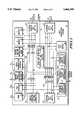
- FIG. 1illustrates in block diagram form, a data processing system in accordance with the present invention.
- FIG. 2illustrates in block diagram form, the data arithmetic logic unit of the data processing system of FIG. 1.
- FIG. 3illustrates a 16-bit multiply/accumulate operation and data alignment in various registers in accordance with an embodiment of the present invention.
- FIG. 4illustrates in block diagram form, a status register of the program control unit of FIG. 1.
- the present inventionprovides for reduced power consumption in a pipelined data ALU. Power consumption is reduced by eliminating unnecessary write backs to the same destination register following a MAC operation.
- a series of instructions provided to the data ALUare monitored. When two or more consecutive instructions having identical destinations for a result are detected, the result is written to a pipeline register instead of to the destination register named in the consecutive instructions. Thus, only a short, lightly loaded bus to the pipeline register is driven, instead of the longer heavily loaded bus to the destination register, resulting in significant power reduction.
- assertand “negate” will be used when referring to the rendering of a signal, status bit, or similar apparatus into its logically true or logically false state, respectively. If the logically true state is a digital logic level one, the logically false state will be a digital logic level zero. And if the logically true state is a digital logic level zero, the logically false state will be a digital logic level one.
- buswill be used to refer to a plurality of signals which may be used to transfer one or more various types of information, such as data, addresses, control, or status.
- FIG. 1illustrates in block diagram form, data processing system 20 in accordance with the present invention.
- data processing system 20is a digital signal processor (DSP) and is located on a single integrated circuit.
- DSPdigital signal processor
- data processing system 20may be, for example, a microcomputer or a microprocessor.
- Data processing system 20includes timer 22, host interface 24, enhanced serial synchronous interface (ESSI) 26, serial asynchronous interface (SCI) 28, program RAM (random access memory) and instruction cache 30, X memory 32, Y memory 34, address generation unit/direct memory access (DMA) controller 36, external address bus switch 38, internal data bus switch 40, DRAM (dynamic random access memory) and SRAM (static random access memory) bus interface and instruction cache control 42, external data bus switch 44, program control unit (PCU) 46, and data arithmetic unit (ALU) 54.
- Program control unit 46includes program interrupt controller 48, program decode controller 50, and program address generator 52.
- Address bus 56labeled “YAB”
- address bus 57labeled “XAB”
- program address bus 58labeled “PAB”
- address bus 59labeled “DAB”
- Data bus 60labeled “DDB”
- Data bus 61labeled “YDB”
- data bus 62labeled “XDB”
- program data bus 63labeled "PDB”
- program data bus 64labeled "GDB” are coupled between internal data bus switch 40 and external data bus switch 44.
- Timer 22includes three timers that can use internal or external timing, and can interrupt data processing system 20 or signal an external device. In addition, timer 22 can be used to signal a DMA transfer after a specified number of events have occurred. Each of the three timers is coupled to a single bi-directional pin or terminal. In addition, each timer of timer 22 is coupled to bus 57, bus 59, program interrupt controller 48, and to bus 60.
- Host interface 24provides a bi-directional interface for communications between data processing system 20 and another device such as a microcomputer, microprocessor, or DMA controller. Also, host interface 24 is bi-directionally coupled to external data bus switch 44 via bus 60, bi-directionally coupled to global data bus 64, to program interrupt controller 48, to address generation unit/DMA controller 36, and to external address bus switch 38 via buses 57 and 59. In addition, host interface 24 is bi-directionally coupled to 50 external pins or terminals for bi-directional data transfers, address register selections, and control communications from a host processor.
- Enhanced serial synchronous interface (ESSI) 26is coupled to 12 bi-directional external pins to provide serial communication with external serial devices including, for example, one or more industry standard codecs, DSPs (digital signal processors), or microprocessors.
- ESSI 26also has terminals coupled to bus 57, bus 59, and bus 60.
- Serial communication interface (SCI) 28is coupled to 3 bi-directional external pins for providing serial communication with external devices. SCI 28 also has terminals coupled to bus 57, bus 59, and bus 60.
- the embodiment of data processing system 20 illustrated in FIG. 1has three memory spaces: program RAM and instruction cache 30, X memory 32, and Y memory 34. In other embodiments, there may be more or fewer memory spaces.
- Program RAM and instruction cache 30is coupled to address bus 58 and to data bus 63.
- X memory 32is coupled to address bus 57, address bus 59, data bus 60, and to data bus 62.
- Y memory 34is coupled to address bus 56, address bus 59, data bus 60, and to data bus 61.
- Address generation unit/DMA controller 36is coupled to address buses 6, 57, 58, and 59. Address generation unit/DMA controller 36 provides memory addresses to timer 22, host interface 24, ESSI 26, SCI 28, program RAM and instruction cache 30, X memory 32, Y memory 34, external address bus switch 38, and to DRAM and SRAM bus interface and instruction cache control 42. In a preferred embodiment, the DMA controller has six channels.
- DRAM and SRAM bus interface and instruction cache 42is coupled to program address bus 58 and to 14 bi-directional external pins.
- the instruction cache of DRAM and SRAM bus interface and instruction cache 42functions as a buffer memory between external main memory (not shown) and program control unit 46.
- the instruction cachestores program instructions that are frequently used. An increase in performance may result when instruction words required by a program are available in the cache, because time required to access the main memory is eliminated.
- Internal data bus switch 40is coupled to data bus 60, data bus 61, data bus 62, program data bus 63, and to global data bus 64.
- External data bus switch 44is coupled to internal data bus switch 40 via data bus 60, data bus 61, data bus 62, program data bus 63, and to global data bus 64.
- external data bus switch 44is coupled to timer 22, host interface 24, ESSI 26, and SCI 28 via data bus 60.
- Internal data bus switch 40is used for transfers between buses. Any two buses can be connected together through internal data bus switch 40.
- External address bus switch 38 and external data bus switch 44couple external buses (not shown) to any internal address bus and internal data bus, respectively.
- program interrupt controller 48arbitrates among interrupt requests, and is coupled to timer 22, host interface 24, ESSI 26, and SCI 28. Also, program interrupt controller 48 is bi-directionally coupled to global data bus 64 and program decode controller 50. Program decode controller 50 decodes each 24-bit instruction and is bi-directionally coupled to program interrupt controller 48 and to program address generator 52. Program address generator 52 contains all of the hardware needed for program address generation, system stack, and loop control. In addition, program address generator 52 is coupled to program address bus 58 and to program data bus 63.
- Data arithmetic logic unit (ALU) 54is coupled to program data bus 63, data bus 61, and to data bus 62. Data ALU 54 performs all of the arithmetic and logical operations on data operands. Data ALU 54 contains registers which may be read or written over by way of buses 61 and 62. Data ALU 54 is also coupled to bus 63 and to bus 60.
- Clock generator circuits(not shown) provide dock signals to all of the blocks shown in FIG. 1. There is also test circuitry in data processing system 20 that is not shown in FIG. 1.
- FIG. 2illustrates in block diagram form, data arithmetic logic unit (ALU) 54 of data processing system 20 of FIG. 1.
- Data ALU 54performs the arithmetic and logical operations for data processing system 20. Data is stored and operated on in signed fractional format in data ALU 54.
- Data ALU 54includes register file 70, multiplier 76, pipeline registers 78, 90, and 96, accumulator and rounding unit 80, accumulator registers 82, shifter/limiter 86, multiplexer 88, control circuit 89, barrel shifter and bit field unit 92, and accumulator shifter 94.
- Register file 70includes registers 71-74.
- Accumulator registers 82includes accumulator register 83 and accumulator register 84.
- Register files 70are coupled to data buses 61 and 62 for receiving data operands from X memory 32, Y memory 34, or from an external memory location (not shown). Each register of registers 71-74 is a read/write register which can store a 24 bit operand. Registers 71-74 serve as input buffer registers between data buses 61 and 62 and data ALU 54. Output terminals of register file 70 are coupled to input terminals of multiplexer 88 and to input terminals of multiplier 76. Multiplier 76 is an execution unit and comprises a conventional array multiplier such as a modified Booth's multiplier, a Wallace Tree, or the like. Multiplier 76 performs multiply operations on operands represented as fractions.
- an intermediate result of a multiply operationis provided to pipeline registers 78, which temporarily stores the intermediate result prior to providing the intermediate result to accumulator and rounding unit 80.
- Accumulator and rounding unit 80also functions as an execution unit in data ALU 54.
- Data ALU 54is pipelined, and every MAC operation is performed in 2 dock cycles.
- the multiplyis performed by multiplier 76 and an intermediate result is stored in pipeline registers 78.
- the accumulatoris added or subtracted from the intermediate result.
- a new instructioncan be initiated in every dock cycle. Rounding is performed if specified in the instruction. The rounding is either convergent rounding (round to the nearest even), or two's complement rounding. The type of rounding is specified by a rounding bit in the status register of program control unit 46.
- Program control unit 46is illustrated in FIG. 1. The bit in the accumulator register that is rounded is specified by the scaling mode bits in the status register.
- Pipeline registers 78are coupled to output terminals of multiplier 76 for receiving the intermediate result from a multiply operation. Output terminals of pipeline registers 78 provide the intermediate result to input terminals of accumulator and rounding unit 80. The intermediate result is added to an operand stored in one of accumulator registers 83 or 84.
- Pipeline registers 96has input terminals coupled to output terminals of accumulator registers 82, and output terminals coupled to input terminals of accumulator and rounding unit 80 for transferring data from one of accumulator registers 83 or 84 to accumulator and rounding unit 80.
- a final resultis typically stored back in the same register, either accumulator register 83 or 84. However, the final result may be written back to a register of register file 70.
- Accumulator registers 83 and 84each comprises 3 concatenated registers to produce a total of 56 bits.
- a 24-bit general purpose read/write register labeled "A0”stores a 24-bit least significant product (LSP).
- A0comprises bits 0-23 of accumulator register 83.
- a 24-bit read/write register labeled "A1”stores a 24-bit most significant product (MSP).
- MSPmost significant product
- A1comprises bits 24-47 of accumulator register 83.
- An 8-bit read/write register labeled "A2"is a sign extension (EXT) and overflow register.
- A2comprises bits 48-56 of accumulator register 83.
- a 24-bit general purpose read/write register labeled "B0"stores 24-bit LSP.
- B0comprises bits 0-23 of accumulator register 84.
- a 24-bit read/write register labeled "B1”stores a 24-bit MSP.
- B1comprises bits 24-47 of accumulator register 84.
- An 8-bit read/write register labeled "B2"functions as a sign extension and overflow register.
- B2comprises bits 48-56 of accumulator register 84.
- Accumulator registers 82, and register file 70are in a programming model for data processing system 20.
- Output terminals of accumulator registers 82are coupled to input terminals of shifter/limiter 86 for transferring 56 bits of data from accumulator registers 82 to shifter/limiter 86.
- Shifter/limiter 86comprises two conventional asynchronous parallel shifter/limiters. One shifter/limiter is coupled to data bus 61 and the other shifter/limiter is coupled to data bus 62.
- the limitersare used to minimize errors due to overflow. Limiting occurs when the extension registers A2 and B2 are in use and the contents of accumulator register 83 or 84 are to be transmitted over data bus 61 or data bus 62. The limiter will substitute a limited data value with a maximum magnitude.
- extension registers A2 and B2are not being used, then the limiters are disabled.
- the two data limiterscan also be combined to form one 48-bit data limiter for long-word operands.
- the data shifters in shifter/limiter 86can shift data one bit to the left (scale up) or one bit the right (scale down), as well as passing the data unshifted (no scaling).
- the shifterspermit dynamic scaling of fixed-point data without modifying the program code. For example, this permits block floating-point algorithms such as fast Fourier transforms to be implemented in data processing system 20.
- Accumulator shifter 94has input terminals coupled to output terminals of accumulator registers 82, and output terminals coupled to accumulator and rounding unit 80.
- Accumulator shifter 94is an asynchronous parallel shifter for shifting the information of accumulator registers 82. Accumulator shifter 94 then provides the shifted information back to accumulator and rounding unit 80.
- Control circuit 89is coupled to accumulator shifter 94, shifter/limiter 86, and barrel shifter and bit field unit 92. Control circuit 89 performs the control functions for data ALU 54 in response to instructions received from program control unit 46 by way of bus 63. For example, control circuit 89 determines the shifting operations required for a MAC instruction that is performed when data ALU 54 is in 16-bit exact mode.
- Multiplexer 88has input terminals coupled to bus 63 and to register file 70. Output terminals of multiplexer 88 are coupled to input terminals of pipeline registers 90. Output terminals of pipeline registers 90 are coupled to barrel shifter and bit field unit 92. Barrel shifter and bit field unit 92 is coupled to input terminals of accumulator registers 82. Barrel shifter and bit field unit 92 contains a 56-bit parallel bi-directional shifter, and performs multibit left shift, multibit right shift, 1-bit rotate (left or right), bit field merge, insert and extract, count leading bits normalization, and logical operations such as AND, OR, exclusive OR, and NOT. Barrel shifter and bit field unit 92 can perform all of these operations for the 24-bit and 16-bit exact modes of operation. In the 16-bit exact mode, the bit field operations are performed on the appropriate bit position for 16-bit data.
- Data ALU 54provides a complete solution for both 24-bit and 16-bit exact arithmetic.
- An entire instruction setcan be executed in 24-bit mode or 16-bit exact mode, including multiprecision arithmetic.
- the same instructions and hardwareare used in both modes.
- a transition between modesis performed by changing a bit in the status register.
- the 16-bit exact mode of operationallows nearly every operation of data ALU 54 to be performed that can performed in 24-bit mode. For example, in 16-bit exact mode, data ALU 54 performs rounding, double precision multiply, moves and shifts. In addition, all bit field operations can be performed in 16-bit exact mode.
- the 16 least significant bits on the buswill be loaded into the 16 most significant bits of the destination register. Zeros are loaded into the 8 least significant bits of the register.
- a 48-bit registersuch as a register formed by concatenating two registers of registers 71-74
- the 16 least significant bits of bus 62are loaded into the 16 most significant bits of registers 72 or 74
- the 16 least significant bits of bus 61are loaded into the 16 most significant bits of registers 71 or 73.
- the datais first aligned and placed in the execution unit in a predetermined alignment to make the 16-bit exact mode transparent to a user of data processing system 20.
- the use of fractional arithmeticmakes the aligning easier.
- Various multiplexing and shifting circuitsare used to accomplish the necessary alignment for 16-bit exact mode. In 16-bit exact mode, rounding of the arithmetic operation is performed on bit 15 of accumulator portion A1/B1 instead of A0/B0 as accomplished in 24-bit mode.
- the scaling, as well as the shifting/limiting operation of data ALU 54are affected accordingly.
- the steps required to perform a 16-bit exact MAC instruction using data ALU 54are illustrated in FIG. 3 as an example.
- a first 16-bit operandis provided to a register of register file 70, for example, register 71 labeled "X0".
- the first operandmay be provided from X memory 32 or Y memory 34 (FIG. 1).
- a second 16-bit operandis provided to another register of register file 70, for example register 73 labeled "Y0".
- the first and second operandsare stored in the 16 most significant bits of the 24-bit registers 71 and 73.
- the 8 least significant bits of registers 71 and 73are negated, or in the illustrated embodiment, written with logical zeros.
- the first 16-bit operand and the second 16-bit operandare multiplied together in multiplier 76 to obtain a 32-bit product.
- the 32-bit productis stored in the 32 most significant bits of an intermediate result register.
- pipeline registers 78function as the intermediate result register.
- the 32-bit productis added to a third operand which is stored in one of accumulator registers 83 or 84.
- the third operandis shifted in accumulator shifter 94 to align, or match, the format of the 32-bit product, and is provided to accumulator and rounding unit 80.
- the result of the additionis written back to the same accumulator register 83 or 84.
- a result of the multiplication instructionis used as an operand for the accumulate instruction.
- the MAC instructionis executed for a predetermined number of iterations.
- the final resultas written back to accumulator registers 82, or is written to one of the registers in register file 70 for each iteration of the MAC instruction.
- the results of the accumulate operationis written back to the same accumulator register.
- the bus between the accumulator and the accumulator registermay be relatively long and have relatively heavy capacitive loading. Therefore, writing back to the accumulator register after each iteration may consume a significant amount of power.
- Control circuit 89monitors the series of instructions being provided to data ALU 54, and detects all cases where consecutive instructions have identical destinations for the final result. Whenever the same register is the destination of consecutive instructions, the result is only written to pipeline register 78, and not to a destination register named in the consecutive instructions. Thus, only the short, lightly loaded bus to pipeline register 78 is driven, instead of the longer heavily loaded bus to the accumulator register, resulting in significant power reduction.
- FIG. 4illustrates in block diagram form, status register 95 of program control unit 46 of FIG. 1.
- Status register 95is a conventional read/write 24-bit register.
- Status bit 97labeled "SA" controls whether data ALU 54 will perform 24-bit arithmetic or 16-bit exact arithmetic.
- control bit 97When control bit 97 is asserted, the 16-bit exact operating mode is entered.
- Status bit 97is cleared during reset of data processing system 20.
Landscapes
- Engineering & Computer Science (AREA)
- Theoretical Computer Science (AREA)
- Software Systems (AREA)
- Physics & Mathematics (AREA)
- General Physics & Mathematics (AREA)
- General Engineering & Computer Science (AREA)
- Computational Mathematics (AREA)
- Mathematical Analysis (AREA)
- Mathematical Optimization (AREA)
- Pure & Applied Mathematics (AREA)
- Computing Systems (AREA)
- Advance Control (AREA)
- Microcomputers (AREA)
- Complex Calculations (AREA)
Abstract
Description
Claims (14)
Priority Applications (4)
| Application Number | Priority Date | Filing Date | Title |
|---|---|---|---|
| US08/361,405US5666300A (en) | 1994-12-22 | 1994-12-22 | Power reduction in a data processing system using pipeline registers and method therefor |
| GB9525824AGB2296118B (en) | 1994-12-22 | 1995-12-18 | Power reduction in a data processing system using pipeline registers and method therefor |
| KR1019950051134AKR100446564B1 (en) | 1994-12-22 | 1995-12-18 | Data processing system and how to run calculations on it |
| CN95120893ACN1132879A (en) | 1994-12-22 | 1995-12-20 | Power reduction in data processing system using pipeline registers and method therefor |
Applications Claiming Priority (1)
| Application Number | Priority Date | Filing Date | Title |
|---|---|---|---|
| US08/361,405US5666300A (en) | 1994-12-22 | 1994-12-22 | Power reduction in a data processing system using pipeline registers and method therefor |
Publications (1)
| Publication Number | Publication Date |
|---|---|
| US5666300Atrue US5666300A (en) | 1997-09-09 |
Family
ID=23421909
Family Applications (1)
| Application Number | Title | Priority Date | Filing Date |
|---|---|---|---|
| US08/361,405Expired - Fee RelatedUS5666300A (en) | 1994-12-22 | 1994-12-22 | Power reduction in a data processing system using pipeline registers and method therefor |
Country Status (4)
| Country | Link |
|---|---|
| US (1) | US5666300A (en) |
| KR (1) | KR100446564B1 (en) |
| CN (1) | CN1132879A (en) |
| GB (1) | GB2296118B (en) |
Cited By (20)
| Publication number | Priority date | Publication date | Assignee | Title |
|---|---|---|---|---|
| US5870581A (en)* | 1996-12-20 | 1999-02-09 | Oak Technology, Inc. | Method and apparatus for performing concurrent write operations to a single-write-input register file and an accumulator register |
| EP0967544A3 (en)* | 1998-06-25 | 2001-02-14 | Texas Instruments Incorporated | Digital signal processor for data having a large bit-length |
| US6564238B1 (en)* | 1999-10-11 | 2003-05-13 | Samsung Electronics Co., Ltd. | Data processing apparatus and method for performing different word-length arithmetic operations |
| US20030144826A1 (en)* | 2002-01-29 | 2003-07-31 | Mandell Michael I. | Register repositioning method for functional verification systems |
| EP1383041A1 (en)* | 2002-07-17 | 2004-01-21 | St Microelectronics S.A. | Interrupt processing during an Iterative instruction execution |
| WO2005024542A3 (en)* | 2003-09-08 | 2005-05-26 | On Demand Microelectronics Gmb | Digital signal processing device |
| US20050177706A1 (en)* | 2003-03-31 | 2005-08-11 | Lee Ruby B. | Parallel subword instructions for directing results to selected subword locations of data processor result register |
| US20060277241A1 (en)* | 2005-06-01 | 2006-12-07 | Atmel Corporation, A Delaware Corporation | Apparatus and method for performing efficient multiply-accumulate operations in microprocessors |
| US20070239968A1 (en)* | 2006-04-05 | 2007-10-11 | Moyer William C | Data processing system having bit exact instructions and methods therefor |
| US20080229075A1 (en)* | 2007-03-16 | 2008-09-18 | Benjamin Francis Froemming | Microcontroller with low-cost digital signal processing extensions |
| US20080229067A1 (en)* | 2007-03-16 | 2008-09-18 | Benjamin Francis Froemming | Data pointers with fast context switching |
| US7890566B1 (en)* | 2000-02-18 | 2011-02-15 | Texas Instruments Incorporated | Microprocessor with rounding dot product instruction |
| US20110055445A1 (en)* | 2009-09-03 | 2011-03-03 | Azuray Technologies, Inc. | Digital Signal Processing Systems |
| US20110153995A1 (en)* | 2009-12-18 | 2011-06-23 | Electronics And Telecommunications Research Institute | Arithmetic apparatus including multiplication and accumulation, and dsp structure and filtering method using the same |
| US9483266B2 (en) | 2013-03-15 | 2016-11-01 | Intel Corporation | Fusible instructions and logic to provide OR-test and AND-test functionality using multiple test sources |
| US9886277B2 (en) | 2013-03-15 | 2018-02-06 | Intel Corporation | Methods and apparatus for fusing instructions to provide OR-test and AND-test functionality on multiple test sources |
| US10901492B1 (en)* | 2019-03-29 | 2021-01-26 | Amazon Technologies, Inc. | Power reduction in processor pipeline by detecting zeros |
| US11144367B2 (en) | 2019-02-08 | 2021-10-12 | International Business Machines Corporation | Write power optimization for hardware employing pipe-based duplicate register files |
| CN113504893A (en)* | 2021-07-23 | 2021-10-15 | 河南亿秒电子科技有限公司 | Intelligent chip architecture and method for efficiently processing data |
| CN114237550A (en)* | 2021-11-10 | 2022-03-25 | 电子科技大学 | A Multi-input Shift-Sum Accumulator Based on Wallace Tree |
Families Citing this family (4)
| Publication number | Priority date | Publication date | Assignee | Title |
|---|---|---|---|---|
| US7131017B2 (en)* | 2002-08-16 | 2006-10-31 | Carnegie Mellon University | Programmable pipeline fabric having mechanism to terminate signal propagation |
| JP4893154B2 (en)* | 2006-08-21 | 2012-03-07 | 富士通セミコンダクター株式会社 | Image processing apparatus and image processing method |
| CN109656867B (en)* | 2016-11-03 | 2023-05-16 | 中科寒武纪科技股份有限公司 | SLAM arithmetic device and method |
| US11579843B2 (en)* | 2020-06-15 | 2023-02-14 | Micron Technology, Inc. | Bit string accumulation in multiple registers |
Citations (3)
| Publication number | Priority date | Publication date | Assignee | Title |
|---|---|---|---|---|
| US4575812A (en)* | 1984-05-31 | 1986-03-11 | Motorola, Inc. | X×Y Bit array multiplier/accumulator circuit |
| US4843585A (en)* | 1987-09-14 | 1989-06-27 | Motorola, Inc. | Pipelineable structure for efficient multiplication and accumulation operations |
| US5204828A (en)* | 1989-02-10 | 1993-04-20 | Intel Corporation | Bus apparatus having hold registers for parallel processing in a microprocessor |
Family Cites Families (7)
| Publication number | Priority date | Publication date | Assignee | Title |
|---|---|---|---|---|
| GB8401807D0 (en)* | 1984-01-24 | 1984-02-29 | Int Computers Ltd | Pipelined data processing apparatus |
| GB2204431A (en)* | 1987-04-25 | 1988-11-09 | Ferranti Plc | Digital signal processing and transducer array beamforming |
| JPH04119430A (en)* | 1990-09-11 | 1992-04-20 | Mitsubishi Electric Corp | Pipeline control method |
| KR950015181B1 (en)* | 1991-07-01 | 1995-12-23 | 후지쓰 가부시끼가이샤 | Apparatus for sum-of-product operation |
| JPH05174050A (en)* | 1991-12-26 | 1993-07-13 | Matsushita Electric Ind Co Ltd | Series arithmetic unit |
| JPH05257683A (en)* | 1992-03-16 | 1993-10-08 | Sharp Corp | Pipeline structure of large scale integrated circuit |
| JPH06282418A (en)* | 1993-03-30 | 1994-10-07 | N T T Idou Tsuushinmou Kk | Arithmetic unit |
- 1994
- 1994-12-22USUS08/361,405patent/US5666300A/ennot_activeExpired - Fee Related
- 1995
- 1995-12-18KRKR1019950051134Apatent/KR100446564B1/ennot_activeExpired - Fee Related
- 1995-12-18GBGB9525824Apatent/GB2296118B/ennot_activeExpired - Fee Related
- 1995-12-20CNCN95120893Apatent/CN1132879A/enactivePending
Patent Citations (3)
| Publication number | Priority date | Publication date | Assignee | Title |
|---|---|---|---|---|
| US4575812A (en)* | 1984-05-31 | 1986-03-11 | Motorola, Inc. | X×Y Bit array multiplier/accumulator circuit |
| US4843585A (en)* | 1987-09-14 | 1989-06-27 | Motorola, Inc. | Pipelineable structure for efficient multiplication and accumulation operations |
| US5204828A (en)* | 1989-02-10 | 1993-04-20 | Intel Corporation | Bus apparatus having hold registers for parallel processing in a microprocessor |
Non-Patent Citations (2)
| Title |
|---|
| Motorola Inc., "DSP56000 Digital Signal Processor Family Manual", 1992, pp. 3-1 through 3-19. |
| Motorola Inc., DSP56000 Digital Signal Processor Family Manual , 1992, pp. 3 1 through 3 19.* |
Cited By (32)
| Publication number | Priority date | Publication date | Assignee | Title |
|---|---|---|---|---|
| US5870581A (en)* | 1996-12-20 | 1999-02-09 | Oak Technology, Inc. | Method and apparatus for performing concurrent write operations to a single-write-input register file and an accumulator register |
| EP0967544A3 (en)* | 1998-06-25 | 2001-02-14 | Texas Instruments Incorporated | Digital signal processor for data having a large bit-length |
| US6564238B1 (en)* | 1999-10-11 | 2003-05-13 | Samsung Electronics Co., Ltd. | Data processing apparatus and method for performing different word-length arithmetic operations |
| US7890566B1 (en)* | 2000-02-18 | 2011-02-15 | Texas Instruments Incorporated | Microprocessor with rounding dot product instruction |
| US20030144826A1 (en)* | 2002-01-29 | 2003-07-31 | Mandell Michael I. | Register repositioning method for functional verification systems |
| US7783691B2 (en) | 2002-07-17 | 2010-08-24 | Stmicroelectronics S.A. | Sharing of a logic operator having a work register |
| EP1383041A1 (en)* | 2002-07-17 | 2004-01-21 | St Microelectronics S.A. | Interrupt processing during an Iterative instruction execution |
| US7730292B2 (en)* | 2003-03-31 | 2010-06-01 | Hewlett-Packard Development Company, L.P. | Parallel subword instructions for directing results to selected subword locations of data processor result register |
| US20050177706A1 (en)* | 2003-03-31 | 2005-08-11 | Lee Ruby B. | Parallel subword instructions for directing results to selected subword locations of data processor result register |
| US20070033152A1 (en)* | 2003-09-08 | 2007-02-08 | On Demand Microelectronics, Gmbh | Digital signal processing device |
| WO2005024542A3 (en)* | 2003-09-08 | 2005-05-26 | On Demand Microelectronics Gmb | Digital signal processing device |
| US8015229B2 (en)* | 2005-06-01 | 2011-09-06 | Atmel Corporation | Apparatus and method for performing efficient multiply-accumulate operations in microprocessors |
| US20060277241A1 (en)* | 2005-06-01 | 2006-12-07 | Atmel Corporation, A Delaware Corporation | Apparatus and method for performing efficient multiply-accumulate operations in microprocessors |
| US20070239968A1 (en)* | 2006-04-05 | 2007-10-11 | Moyer William C | Data processing system having bit exact instructions and methods therefor |
| US8307196B2 (en) | 2006-04-05 | 2012-11-06 | Freescale Semiconductor, Inc. | Data processing system having bit exact instructions and methods therefor |
| US20080229075A1 (en)* | 2007-03-16 | 2008-09-18 | Benjamin Francis Froemming | Microcontroller with low-cost digital signal processing extensions |
| US20080229067A1 (en)* | 2007-03-16 | 2008-09-18 | Benjamin Francis Froemming | Data pointers with fast context switching |
| US7797516B2 (en)* | 2007-03-16 | 2010-09-14 | Atmel Corporation | Microcontroller with low-cost digital signal processing extensions |
| US8370606B2 (en) | 2007-03-16 | 2013-02-05 | Atmel Corporation | Switching data pointers based on context |
| US20110055445A1 (en)* | 2009-09-03 | 2011-03-03 | Azuray Technologies, Inc. | Digital Signal Processing Systems |
| WO2011028723A3 (en)* | 2009-09-03 | 2011-09-29 | Azuray Technologies, Inc. | Digital signal processing systems |
| US20110055303A1 (en)* | 2009-09-03 | 2011-03-03 | Azuray Technologies, Inc. | Function Generator |
| US20110153995A1 (en)* | 2009-12-18 | 2011-06-23 | Electronics And Telecommunications Research Institute | Arithmetic apparatus including multiplication and accumulation, and dsp structure and filtering method using the same |
| US9483266B2 (en) | 2013-03-15 | 2016-11-01 | Intel Corporation | Fusible instructions and logic to provide OR-test and AND-test functionality using multiple test sources |
| US9886277B2 (en) | 2013-03-15 | 2018-02-06 | Intel Corporation | Methods and apparatus for fusing instructions to provide OR-test and AND-test functionality on multiple test sources |
| US10296347B2 (en) | 2013-03-15 | 2019-05-21 | Intel Corporation | Fusible instructions and logic to provide or-test and and-test functionality using multiple test sources |
| US11144367B2 (en) | 2019-02-08 | 2021-10-12 | International Business Machines Corporation | Write power optimization for hardware employing pipe-based duplicate register files |
| US10901492B1 (en)* | 2019-03-29 | 2021-01-26 | Amazon Technologies, Inc. | Power reduction in processor pipeline by detecting zeros |
| CN113504893A (en)* | 2021-07-23 | 2021-10-15 | 河南亿秒电子科技有限公司 | Intelligent chip architecture and method for efficiently processing data |
| CN113504893B (en)* | 2021-07-23 | 2022-08-26 | 河南亿秒电子科技有限公司 | Intelligent chip architecture and method for efficiently processing data |
| CN114237550A (en)* | 2021-11-10 | 2022-03-25 | 电子科技大学 | A Multi-input Shift-Sum Accumulator Based on Wallace Tree |
| CN114237550B (en)* | 2021-11-10 | 2023-10-13 | 电子科技大学 | Wallace tree-based multi-input shift sum accumulator |
Also Published As
| Publication number | Publication date |
|---|---|
| CN1132879A (en) | 1996-10-09 |
| GB2296118B (en) | 1999-10-06 |
| GB9525824D0 (en) | 1996-02-21 |
| KR960024896A (en) | 1996-07-20 |
| KR100446564B1 (en) | 2004-11-03 |
| GB2296118A (en) | 1996-06-19 |
Similar Documents
| Publication | Publication Date | Title |
|---|---|---|
| US5666300A (en) | Power reduction in a data processing system using pipeline registers and method therefor | |
| US5598362A (en) | Apparatus and method for performing both 24 bit and 16 bit arithmetic | |
| US5422805A (en) | Method and apparatus for multiplying two numbers using signed arithmetic | |
| JP3756967B2 (en) | Multiple bit shift apparatus, data processor using the same, and method thereof | |
| US6564238B1 (en) | Data processing apparatus and method for performing different word-length arithmetic operations | |
| EP0789297B1 (en) | Data processor loading data and performing multiply-add operation in parallel | |
| US4740893A (en) | Method for reducing the time for switching between programs | |
| US6374346B1 (en) | Processor with conditional execution of every instruction | |
| JPH10187438A (en) | How to reduce transitions for multiplier inputs. | |
| US5436860A (en) | Combined multiplier/shifter and method therefor | |
| JP2001501330A (en) | Digital signal processing integrated circuit architecture | |
| JP3403759B2 (en) | Method and processor for writing result of data operation to storage register | |
| US7631207B1 (en) | Reducing power consumption for processing of common values in microprocessor registers and execution units | |
| JPH11504744A (en) | System for performing arithmetic operations in single or double precision | |
| US5958000A (en) | Two-bit booth multiplier with reduced data path width | |
| EP0901067A2 (en) | Method and system for executing operations on denormalised numbers | |
| EP2267596B1 (en) | Processor core for processing instructions of different formats | |
| US7111155B1 (en) | Digital signal processor computation core with input operand selection from operand bus for dual operations | |
| US4631672A (en) | Arithmetic control apparatus for a pipeline processing system | |
| US6820189B1 (en) | Computation core executing multiple operation DSP instructions and micro-controller instructions of shorter length without performing switch operation | |
| EP0260837B1 (en) | Microprocessor with selective cache memory | |
| US7107302B1 (en) | Finite impulse response filter algorithm for implementation on digital signal processor having dual execution units | |
| JP2001501001A (en) | Input operand control in data processing systems | |
| KR100431726B1 (en) | Method for performing signed division | |
| US6859872B1 (en) | Digital signal processor computation core with pipeline having memory access stages and multiply accumulate stages positioned for efficient operation |
Legal Events
| Date | Code | Title | Description |
|---|---|---|---|
| AS | Assignment | Owner name:MOTOROLA, INC., ILLINOIS Free format text:ASSIGNMENT OF ASSIGNORS INTEREST;ASSIGNORS:ADELMAN, JUDAH L.;GALANTI, DAVID;SALANT, YORAM;REEL/FRAME:007418/0844;SIGNING DATES FROM 19950216 TO 19950228 | |
| FPAY | Fee payment | Year of fee payment:4 | |
| AS | Assignment | Owner name:FREESCALE SEMICONDUCTOR, INC., TEXAS Free format text:ASSIGNMENT OF ASSIGNORS INTEREST;ASSIGNOR:MOTOROLA, INC.;REEL/FRAME:015698/0657 Effective date:20040404 Owner name:FREESCALE SEMICONDUCTOR, INC.,TEXAS Free format text:ASSIGNMENT OF ASSIGNORS INTEREST;ASSIGNOR:MOTOROLA, INC.;REEL/FRAME:015698/0657 Effective date:20040404 | |
| FPAY | Fee payment | Year of fee payment:8 | |
| AS | Assignment | Owner name:CITIBANK, N.A. AS COLLATERAL AGENT, NEW YORK Free format text:SECURITY AGREEMENT;ASSIGNORS:FREESCALE SEMICONDUCTOR, INC.;FREESCALE ACQUISITION CORPORATION;FREESCALE ACQUISITION HOLDINGS CORP.;AND OTHERS;REEL/FRAME:018855/0129 Effective date:20061201 Owner name:CITIBANK, N.A. AS COLLATERAL AGENT,NEW YORK Free format text:SECURITY AGREEMENT;ASSIGNORS:FREESCALE SEMICONDUCTOR, INC.;FREESCALE ACQUISITION CORPORATION;FREESCALE ACQUISITION HOLDINGS CORP.;AND OTHERS;REEL/FRAME:018855/0129 Effective date:20061201 | |
| REMI | Maintenance fee reminder mailed | ||
| LAPS | Lapse for failure to pay maintenance fees | ||
| STCH | Information on status: patent discontinuation | Free format text:PATENT EXPIRED DUE TO NONPAYMENT OF MAINTENANCE FEES UNDER 37 CFR 1.362 | |
| FP | Lapsed due to failure to pay maintenance fee | Effective date:20090909 | |
| AS | Assignment | Owner name:FREESCALE SEMICONDUCTOR, INC., TEXAS Free format text:PATENT RELEASE;ASSIGNOR:CITIBANK, N.A., AS COLLATERAL AGENT;REEL/FRAME:037354/0225 Effective date:20151207 |