US5666270A - Bump electrode, semiconductor integrated circuit device using the same, multi-chip module having the semiconductor integrated circuit devices and method for producing semicondutcor device having the bump electrode - Google Patents
Bump electrode, semiconductor integrated circuit device using the same, multi-chip module having the semiconductor integrated circuit devices and method for producing semicondutcor device having the bump electrodeDownload PDFInfo
- Publication number
- US5666270A US5666270AUS08/280,327US28032794AUS5666270AUS 5666270 AUS5666270 AUS 5666270AUS 28032794 AUS28032794 AUS 28032794AUS 5666270 AUS5666270 AUS 5666270A
- Authority
- US
- United States
- Prior art keywords
- conductive film
- electrically conductive
- electrode
- bump electrode
- bump
- Prior art date
- Legal status (The legal status is an assumption and is not a legal conclusion. Google has not performed a legal analysis and makes no representation as to the accuracy of the status listed.)
- Expired - Lifetime
Links
Images


Classifications
- H—ELECTRICITY
- H01—ELECTRIC ELEMENTS
- H01L—SEMICONDUCTOR DEVICES NOT COVERED BY CLASS H10
- H01L24/00—Arrangements for connecting or disconnecting semiconductor or solid-state bodies; Methods or apparatus related thereto
- H01L24/80—Methods for connecting semiconductor or other solid state bodies using means for bonding being attached to, or being formed on, the surface to be connected
- H01L24/81—Methods for connecting semiconductor or other solid state bodies using means for bonding being attached to, or being formed on, the surface to be connected using a bump connector
- H—ELECTRICITY
- H01—ELECTRIC ELEMENTS
- H01L—SEMICONDUCTOR DEVICES NOT COVERED BY CLASS H10
- H01L24/00—Arrangements for connecting or disconnecting semiconductor or solid-state bodies; Methods or apparatus related thereto
- H01L24/01—Means for bonding being attached to, or being formed on, the surface to be connected, e.g. chip-to-package, die-attach, "first-level" interconnects; Manufacturing methods related thereto
- H01L24/10—Bump connectors ; Manufacturing methods related thereto
- H01L24/11—Manufacturing methods
- H—ELECTRICITY
- H01—ELECTRIC ELEMENTS
- H01L—SEMICONDUCTOR DEVICES NOT COVERED BY CLASS H10
- H01L24/00—Arrangements for connecting or disconnecting semiconductor or solid-state bodies; Methods or apparatus related thereto
- H01L24/01—Means for bonding being attached to, or being formed on, the surface to be connected, e.g. chip-to-package, die-attach, "first-level" interconnects; Manufacturing methods related thereto
- H01L24/10—Bump connectors ; Manufacturing methods related thereto
- H01L24/12—Structure, shape, material or disposition of the bump connectors prior to the connecting process
- H01L24/13—Structure, shape, material or disposition of the bump connectors prior to the connecting process of an individual bump connector
- H—ELECTRICITY
- H01—ELECTRIC ELEMENTS
- H01L—SEMICONDUCTOR DEVICES NOT COVERED BY CLASS H10
- H01L24/00—Arrangements for connecting or disconnecting semiconductor or solid-state bodies; Methods or apparatus related thereto
- H01L24/74—Apparatus for manufacturing arrangements for connecting or disconnecting semiconductor or solid-state bodies
- H01L24/75—Apparatus for connecting with bump connectors or layer connectors
- H—ELECTRICITY
- H01—ELECTRIC ELEMENTS
- H01L—SEMICONDUCTOR DEVICES NOT COVERED BY CLASS H10
- H01L2224/00—Indexing scheme for arrangements for connecting or disconnecting semiconductor or solid-state bodies and methods related thereto as covered by H01L24/00
- H01L2224/01—Means for bonding being attached to, or being formed on, the surface to be connected, e.g. chip-to-package, die-attach, "first-level" interconnects; Manufacturing methods related thereto
- H01L2224/02—Bonding areas; Manufacturing methods related thereto
- H01L2224/04—Structure, shape, material or disposition of the bonding areas prior to the connecting process
- H01L2224/05—Structure, shape, material or disposition of the bonding areas prior to the connecting process of an individual bonding area
- H01L2224/05001—Internal layers
- H01L2224/05099—Material
- H01L2224/051—Material with a principal constituent of the material being a metal or a metalloid, e.g. boron [B], silicon [Si], germanium [Ge], arsenic [As], antimony [Sb], tellurium [Te] and polonium [Po], and alloys thereof
- H01L2224/05117—Material with a principal constituent of the material being a metal or a metalloid, e.g. boron [B], silicon [Si], germanium [Ge], arsenic [As], antimony [Sb], tellurium [Te] and polonium [Po], and alloys thereof the principal constituent melting at a temperature of greater than or equal to 400°C and less than 950°C
- H01L2224/05124—Aluminium [Al] as principal constituent
- H—ELECTRICITY
- H01—ELECTRIC ELEMENTS
- H01L—SEMICONDUCTOR DEVICES NOT COVERED BY CLASS H10
- H01L2224/00—Indexing scheme for arrangements for connecting or disconnecting semiconductor or solid-state bodies and methods related thereto as covered by H01L24/00
- H01L2224/01—Means for bonding being attached to, or being formed on, the surface to be connected, e.g. chip-to-package, die-attach, "first-level" interconnects; Manufacturing methods related thereto
- H01L2224/10—Bump connectors; Manufacturing methods related thereto
- H01L2224/12—Structure, shape, material or disposition of the bump connectors prior to the connecting process
- H01L2224/13—Structure, shape, material or disposition of the bump connectors prior to the connecting process of an individual bump connector
- H01L2224/13001—Core members of the bump connector
- H01L2224/13099—Material
- H01L2224/131—Material with a principal constituent of the material being a metal or a metalloid, e.g. boron [B], silicon [Si], germanium [Ge], arsenic [As], antimony [Sb], tellurium [Te] and polonium [Po], and alloys thereof
- H01L2224/13101—Material with a principal constituent of the material being a metal or a metalloid, e.g. boron [B], silicon [Si], germanium [Ge], arsenic [As], antimony [Sb], tellurium [Te] and polonium [Po], and alloys thereof the principal constituent melting at a temperature of less than 400°C
- H01L2224/13111—Tin [Sn] as principal constituent
- H—ELECTRICITY
- H01—ELECTRIC ELEMENTS
- H01L—SEMICONDUCTOR DEVICES NOT COVERED BY CLASS H10
- H01L2224/00—Indexing scheme for arrangements for connecting or disconnecting semiconductor or solid-state bodies and methods related thereto as covered by H01L24/00
- H01L2224/01—Means for bonding being attached to, or being formed on, the surface to be connected, e.g. chip-to-package, die-attach, "first-level" interconnects; Manufacturing methods related thereto
- H01L2224/10—Bump connectors; Manufacturing methods related thereto
- H01L2224/15—Structure, shape, material or disposition of the bump connectors after the connecting process
- H01L2224/16—Structure, shape, material or disposition of the bump connectors after the connecting process of an individual bump connector
- H—ELECTRICITY
- H01—ELECTRIC ELEMENTS
- H01L—SEMICONDUCTOR DEVICES NOT COVERED BY CLASS H10
- H01L2224/00—Indexing scheme for arrangements for connecting or disconnecting semiconductor or solid-state bodies and methods related thereto as covered by H01L24/00
- H01L2224/01—Means for bonding being attached to, or being formed on, the surface to be connected, e.g. chip-to-package, die-attach, "first-level" interconnects; Manufacturing methods related thereto
- H01L2224/42—Wire connectors; Manufacturing methods related thereto
- H01L2224/47—Structure, shape, material or disposition of the wire connectors after the connecting process
- H01L2224/48—Structure, shape, material or disposition of the wire connectors after the connecting process of an individual wire connector
- H01L2224/4805—Shape
- H01L2224/4809—Loop shape
- H01L2224/48091—Arched
- H—ELECTRICITY
- H01—ELECTRIC ELEMENTS
- H01L—SEMICONDUCTOR DEVICES NOT COVERED BY CLASS H10
- H01L2224/00—Indexing scheme for arrangements for connecting or disconnecting semiconductor or solid-state bodies and methods related thereto as covered by H01L24/00
- H01L2224/01—Means for bonding being attached to, or being formed on, the surface to be connected, e.g. chip-to-package, die-attach, "first-level" interconnects; Manufacturing methods related thereto
- H01L2224/42—Wire connectors; Manufacturing methods related thereto
- H01L2224/47—Structure, shape, material or disposition of the wire connectors after the connecting process
- H01L2224/48—Structure, shape, material or disposition of the wire connectors after the connecting process of an individual wire connector
- H01L2224/481—Disposition
- H01L2224/48151—Connecting between a semiconductor or solid-state body and an item not being a semiconductor or solid-state body, e.g. chip-to-substrate, chip-to-passive
- H01L2224/48221—Connecting between a semiconductor or solid-state body and an item not being a semiconductor or solid-state body, e.g. chip-to-substrate, chip-to-passive the body and the item being stacked
- H01L2224/48225—Connecting between a semiconductor or solid-state body and an item not being a semiconductor or solid-state body, e.g. chip-to-substrate, chip-to-passive the body and the item being stacked the item being non-metallic, e.g. insulating substrate with or without metallisation
- H01L2224/48227—Connecting between a semiconductor or solid-state body and an item not being a semiconductor or solid-state body, e.g. chip-to-substrate, chip-to-passive the body and the item being stacked the item being non-metallic, e.g. insulating substrate with or without metallisation connecting the wire to a bond pad of the item
- H—ELECTRICITY
- H01—ELECTRIC ELEMENTS
- H01L—SEMICONDUCTOR DEVICES NOT COVERED BY CLASS H10
- H01L2224/00—Indexing scheme for arrangements for connecting or disconnecting semiconductor or solid-state bodies and methods related thereto as covered by H01L24/00
- H01L2224/01—Means for bonding being attached to, or being formed on, the surface to be connected, e.g. chip-to-package, die-attach, "first-level" interconnects; Manufacturing methods related thereto
- H01L2224/42—Wire connectors; Manufacturing methods related thereto
- H01L2224/47—Structure, shape, material or disposition of the wire connectors after the connecting process
- H01L2224/48—Structure, shape, material or disposition of the wire connectors after the connecting process of an individual wire connector
- H01L2224/484—Connecting portions
- H01L2224/48463—Connecting portions the connecting portion on the bonding area of the semiconductor or solid-state body being a ball bond
- H01L2224/48465—Connecting portions the connecting portion on the bonding area of the semiconductor or solid-state body being a ball bond the other connecting portion not on the bonding area being a wedge bond, i.e. ball-to-wedge, regular stitch
- H—ELECTRICITY
- H01—ELECTRIC ELEMENTS
- H01L—SEMICONDUCTOR DEVICES NOT COVERED BY CLASS H10
- H01L2224/00—Indexing scheme for arrangements for connecting or disconnecting semiconductor or solid-state bodies and methods related thereto as covered by H01L24/00
- H01L2224/73—Means for bonding being of different types provided for in two or more of groups H01L2224/10, H01L2224/18, H01L2224/26, H01L2224/34, H01L2224/42, H01L2224/50, H01L2224/63, H01L2224/71
- H01L2224/732—Location after the connecting process
- H01L2224/73251—Location after the connecting process on different surfaces
- H01L2224/73253—Bump and layer connectors
- H—ELECTRICITY
- H01—ELECTRIC ELEMENTS
- H01L—SEMICONDUCTOR DEVICES NOT COVERED BY CLASS H10
- H01L2224/00—Indexing scheme for arrangements for connecting or disconnecting semiconductor or solid-state bodies and methods related thereto as covered by H01L24/00
- H01L2224/74—Apparatus for manufacturing arrangements for connecting or disconnecting semiconductor or solid-state bodies and for methods related thereto
- H01L2224/75—Apparatus for connecting with bump connectors or layer connectors
- H—ELECTRICITY
- H01—ELECTRIC ELEMENTS
- H01L—SEMICONDUCTOR DEVICES NOT COVERED BY CLASS H10
- H01L2224/00—Indexing scheme for arrangements for connecting or disconnecting semiconductor or solid-state bodies and methods related thereto as covered by H01L24/00
- H01L2224/80—Methods for connecting semiconductor or other solid state bodies using means for bonding being attached to, or being formed on, the surface to be connected
- H01L2224/81—Methods for connecting semiconductor or other solid state bodies using means for bonding being attached to, or being formed on, the surface to be connected using a bump connector
- H01L2224/818—Bonding techniques
- H01L2224/81801—Soldering or alloying
- H—ELECTRICITY
- H01—ELECTRIC ELEMENTS
- H01L—SEMICONDUCTOR DEVICES NOT COVERED BY CLASS H10
- H01L2924/00—Indexing scheme for arrangements or methods for connecting or disconnecting semiconductor or solid-state bodies as covered by H01L24/00
- H01L2924/01—Chemical elements
- H01L2924/01005—Boron [B]
- H—ELECTRICITY
- H01—ELECTRIC ELEMENTS
- H01L—SEMICONDUCTOR DEVICES NOT COVERED BY CLASS H10
- H01L2924/00—Indexing scheme for arrangements or methods for connecting or disconnecting semiconductor or solid-state bodies as covered by H01L24/00
- H01L2924/01—Chemical elements
- H01L2924/01006—Carbon [C]
- H—ELECTRICITY
- H01—ELECTRIC ELEMENTS
- H01L—SEMICONDUCTOR DEVICES NOT COVERED BY CLASS H10
- H01L2924/00—Indexing scheme for arrangements or methods for connecting or disconnecting semiconductor or solid-state bodies as covered by H01L24/00
- H01L2924/01—Chemical elements
- H01L2924/01013—Aluminum [Al]
- H—ELECTRICITY
- H01—ELECTRIC ELEMENTS
- H01L—SEMICONDUCTOR DEVICES NOT COVERED BY CLASS H10
- H01L2924/00—Indexing scheme for arrangements or methods for connecting or disconnecting semiconductor or solid-state bodies as covered by H01L24/00
- H01L2924/01—Chemical elements
- H01L2924/01033—Arsenic [As]
- H—ELECTRICITY
- H01—ELECTRIC ELEMENTS
- H01L—SEMICONDUCTOR DEVICES NOT COVERED BY CLASS H10
- H01L2924/00—Indexing scheme for arrangements or methods for connecting or disconnecting semiconductor or solid-state bodies as covered by H01L24/00
- H01L2924/01—Chemical elements
- H01L2924/0105—Tin [Sn]
- H—ELECTRICITY
- H01—ELECTRIC ELEMENTS
- H01L—SEMICONDUCTOR DEVICES NOT COVERED BY CLASS H10
- H01L2924/00—Indexing scheme for arrangements or methods for connecting or disconnecting semiconductor or solid-state bodies as covered by H01L24/00
- H01L2924/01—Chemical elements
- H01L2924/01078—Platinum [Pt]
- H—ELECTRICITY
- H01—ELECTRIC ELEMENTS
- H01L—SEMICONDUCTOR DEVICES NOT COVERED BY CLASS H10
- H01L2924/00—Indexing scheme for arrangements or methods for connecting or disconnecting semiconductor or solid-state bodies as covered by H01L24/00
- H01L2924/01—Chemical elements
- H01L2924/01079—Gold [Au]
- H—ELECTRICITY
- H01—ELECTRIC ELEMENTS
- H01L—SEMICONDUCTOR DEVICES NOT COVERED BY CLASS H10
- H01L2924/00—Indexing scheme for arrangements or methods for connecting or disconnecting semiconductor or solid-state bodies as covered by H01L24/00
- H01L2924/01—Chemical elements
- H01L2924/01082—Lead [Pb]
- H—ELECTRICITY
- H01—ELECTRIC ELEMENTS
- H01L—SEMICONDUCTOR DEVICES NOT COVERED BY CLASS H10
- H01L2924/00—Indexing scheme for arrangements or methods for connecting or disconnecting semiconductor or solid-state bodies as covered by H01L24/00
- H01L2924/013—Alloys
- H01L2924/014—Solder alloys
- H—ELECTRICITY
- H01—ELECTRIC ELEMENTS
- H01L—SEMICONDUCTOR DEVICES NOT COVERED BY CLASS H10
- H01L2924/00—Indexing scheme for arrangements or methods for connecting or disconnecting semiconductor or solid-state bodies as covered by H01L24/00
- H01L2924/10—Details of semiconductor or other solid state devices to be connected
- H01L2924/11—Device type
- H01L2924/14—Integrated circuits
- H—ELECTRICITY
- H01—ELECTRIC ELEMENTS
- H01L—SEMICONDUCTOR DEVICES NOT COVERED BY CLASS H10
- H01L2924/00—Indexing scheme for arrangements or methods for connecting or disconnecting semiconductor or solid-state bodies as covered by H01L24/00
- H01L2924/15—Details of package parts other than the semiconductor or other solid state devices to be connected
- H01L2924/151—Die mounting substrate
- H01L2924/153—Connection portion
- H01L2924/1531—Connection portion the connection portion being formed only on the surface of the substrate opposite to the die mounting surface
- H01L2924/15312—Connection portion the connection portion being formed only on the surface of the substrate opposite to the die mounting surface being a pin array, e.g. PGA
- H—ELECTRICITY
- H01—ELECTRIC ELEMENTS
- H01L—SEMICONDUCTOR DEVICES NOT COVERED BY CLASS H10
- H01L2924/00—Indexing scheme for arrangements or methods for connecting or disconnecting semiconductor or solid-state bodies as covered by H01L24/00
- H01L2924/15—Details of package parts other than the semiconductor or other solid state devices to be connected
- H01L2924/161—Cap
- H01L2924/1615—Shape
- H01L2924/16195—Flat cap [not enclosing an internal cavity]
Definitions
- the present inventiongenerally relates to semiconductor integrated circuit devices, and more particularly to a bump electrode used in such devices. More particularly, the present invention is concerned with a bump electrode for flip chip mounting.
- a flip chip mounting method utilizing bump electrodesis known as a method for achieving high-density mounting of semiconductor elements.
- ithas been desired to lengthen the fatigue-based duration of life in regard to a temperature cycle.
- An object of the present inventionis to provide a bump electrode having a longer fatigue-based duration of life.
- a bump electrodecomprising: a core portion provided on an intermediate electrode layer formed on an electrode pad formed on a surface of an element, the core portion containing a material having a Young's modulus less than that of soldering; and an electrically conductive film covering the core portion.
- the core portioncomprises silicone resin, and the core portion has a dome shape.
- a protection filmwhich covers the electrically conductive film except for a portion of the electrically conductive film. The portion of the electrically conductive film is to be in contact with an electrode formed on a member on which the element should be mounted.
- the protection filmcomprises an insulating material.
- Another object of the present inventionis to provide a semiconductor device equipped with such a bump electrode.
- a semiconductor devicecomprising: a chip; and a plurality of bump electrodes, each of the bump electrodes comprising: a core portion provided on an intermediate electrode layer formed on an electrode pad formed on a surface of the chip, the core portion containing a material having a Young's modulus less than that of soldering; and an electrically conductive film covering the core portion.
- a semiconductor devicecomprising: a chip; a plurality of bump electrodes; a circuit board having pads which are in contact with the plurality of bumps; a package base supporting the circuit board and having terminals connected to the pads; and leads electrically connecting the circuit board to the terminals of the package base.
- Each of the bump electrodescomprises: a core portion provided on an intermediate electrode layer formed on an electrode pad formed on a surface of the chip, the core portion containing a material having a Young's modulus less than that of solder; and an electrically conductive film covering the core portion.
- Yet another object of the present inventionis to provide a method for producing the above-mentioned bump electrode.
- a method for producing a semiconductor device having a prior art bump electrode as described abovecomprising the steps of: (a) forming a core portion on an intermediate electrode layer formed on an electrode pad formed on a surface of an element, the core portion containing a material having a Young's modulus less than that of soldering; and (b) forming an electrically conductive film covering the core portion.
- the step (a)comprises steps of: (a-1) forming an ultraviolet-hardening silicone resin on the surface of the element; and (a-2) patterning the ultraviolet-hardening silicon resin so that a projection of the ultraviolet-hardening silicon resin is formed, the projection corresponding to the core portion of the bump electrode.
- the step (a-2)further comprises the step of removing edges of the projection.
- the methodfurther comprises the step (c) of forming a protection film which covers the electrically conductive film except for a portion of the electrically conductive film, the portion of the electrically conductive film to be in contact with an electrode formed on a member on which the element should be mounted, the protection film comprising an insulating material.
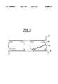
- FIG. 1is a cross-sectional view of a prior art bump electrode related to the present invention
- FIG. 2is an enlarged side view of flip-chip mounting utilizing the bump electrode shown in FIG. 1;
- FIG. 3is a diagram showing a disadvantage of the bump electrode shown in FIGS. 1 and 2;
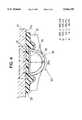
- FIG. 4is a cross-sectional view of a prior art bump electrode according to an embodiment of the present invention.
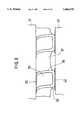
- FIG. 5is a side view of a multi-chip module using the bump electrode shown in FIG. 4;
- FIG. 6is a side view showing advantages of the present invention.
- FIGS. 7A, 7B, 7C, 7D, 7E and 7Fare diagrams of a method of producing the bump electrode shown in FIG. 4.
- FIG. 1is a cross-sectional view of a prior art bump electrode 10 related to the present invention.
- An electrode pad 12 and a protection film 13are formed on a lower surface 11a of a semiconductor element 11.
- the bump electrode 10is formed so that a soldering bump 14 is provided on the electrode pad 12 via a metallic intermediate layer 15.
- FIG. 2shows a semiconductor device 17 in which the semiconductor element 11 equipped with the bump electrode 10 is flip-chip mounted on a mounting circuit board 16.
- the semiconductor device 17radiates heat during operation. When the semiconductor device 17 stops operating, it is cooled to the room temperature and subjected to a temperature cycle.
- the soldering bump 14is an alloy of Pb/Sn (9:1), and the Young's modulus is as high as 1.9 ⁇ 10 3 (kgf/mm 2 ), so that the soldering bump 14 is not likely to deform.
- the semiconductor element 11is made of silicon, and the coefficient of thermal expansion thereof is 3.5 ⁇ 10 -6 (1/°C.).
- the mounting circuit board 16is made of AlN or glass epoxy resin. The coefficient of thermal expansion of AlN is 4.2 ⁇ 10 -6 (1/°C.), and the coefficient of thermal expansion of glass epoxy resin is 12.0 ⁇ 10 -6 (1/°C.).
- the inventorsobtained, by a computer simulation, the fatigue-based duration of life of bump electrode 10 (soldering bump 14) in accordance with the temperature cycle. Even when the AlN mounting circuit board 16 is used in such a way that the difference in the coefficient of thermal expansion is reduced, the fatigue-based duration of life of the bump electrode 10 (soldering bump 14) was approximately 2600 times.
- soldering bump 14is broken as indicated by reference number 19, and accordingly, electric conduction is broken in soldering bump 14.
- the duration of life of 2600 temperature cyclesis not a sufficiently long period of time.
- the mounting circuit board 16is made of glass epoxy resin in order to reduce the production cost of the semiconductor device 17, there is a large difference between the coefficient of thermal expansion of the semiconductor element 11 and that of the mounting circuit board 16. Hence, the duration of life will be greatly shorter than the duration of life of 2600 temperature cycles.
- the present inventionis intended to lengthen the duration of life of bump electrodes and thus semiconductor devices equipped with such bump electrodes.
- FIG. 4shows a prior art bump electrode 30 according to an embodiment of the present invention.
- a semiconductor element 31such as a chip to be mounted, is made of silicon, and has a lower surface 31a on which an electrode pad 32, made of aluminum, is formed.
- the electrode pad 32has a diameter a of 200 to 300 ⁇ m.
- the lower surface 31a of the semiconductor element 31is covered by a protection film 33 made of C-PSG except for the electrode pad 32.
- the electrode pad 32is covered by a metallic intermediate layer 34 serving as a metal barrier layer.
- the bump electrode 30will be described below.
- the bump electrode 30is made up of a core portion 35 and an electrically conductive film 36.
- the core part 35 of the bump electrode 30is made of UV (Ultraviolet)-hardening silicone resin marketed by SHINETSU SILICONE COMPANY in Japan.
- the core portion 35has a reverse dome shape and is formed on the metallic intermediate layer 34.
- the core portion 35has a diameter b of 150 to 200 ⁇ m, and a height of 50 to 150 ⁇ m.
- the Young's modulus of the UV-hardening silicone resinis 1.4 ⁇ 10 1 (kgf/cm 2 ), and is approximately equal to 1/100 of the Young's modulus of soldering. Hence, the core portion 35 has a small stiffness and is flexible.
- the conductive film 36is made of gold (Au) and covers the whole surface of the core portion 35.
- the conductive film 36is electrically connected to the surface of the metallic intermediate layer 34.
- the conductive film 36is 5 to 20 ⁇ m thick.
- the core portion 35has a small stiffness and is flexible, and is easily deformed by a small magnitude of external force. Also, the conductive film 36 is easily deformed in response to a deformation of the core portion 35. Hence, the bump electrode 30 is easily deformed by an external force, as indicated by the two-dot chained lines shown in FIG. 4.
- the bump electrode 30is covered by the protection film 37 except for the lowermost (apex) portion 30a, the protection film 37 being made of thermoplastic silicone resin.
- the protection film 37is provided taking into account the fact that the adhesion between the conductive film 36 and the core portion 35 is weak.
- the protection film 37presses down the conductive film 36 in order to prevent the conductive film 36 from coming off from the core portion 35.
- the protection film 37covers the periphery of the bump electrode 30.
- the protection film 37has a small Young's modulus of 1.4 ⁇ 10 1 (kgf/mm 2 ), and is flexible. Hence, the protection film 37 prevents deformations of the bump electrode 30.
- FIG. 5is a multi-chip module having bump electrodes having the structure shown in FIG. 4.
- a plurality (two in FIG. 5) of semiconductor elements 31are mounted on an AlN mounting circuit board 41 by the flip-chip method utilizing bump electrodes 30.
- the bump electrodes 30have lowermost portions, which are electrically connected to electrode pads 42 provided on the mounting circuit board 41.
- the semiconductor elements 31 and the mounting circuit board 41are electrically connected via the conductive films 36 of the bump electrodes 30.
- the mounting circuit board 41is fastened to the upper surface of a package base 43. Electrodes 51 formed on the mounting circuit board 41 are electrically connected to pads 49 formed on the upper surface of the package base 43 by means of wires 45. The pads formed on the upper surface of the package base 43 are electrically connected to pin terminals 44, which project from the lower surface of the package base 43.
- a heat sink 46 to which the semiconductor elements 31 are attachedis supported by a seal ring 47 placed on the upper surface of the package base 43, so that the semiconductor elements 31 and the mounting circuit base 41 are sealed.
- the multi-chip module 40While the multi-chip module 40 is operating, it radiates heats and the semiconductor elements 31 and mounting circuit board 41 are thermally expanded. A mismatch between the coefficient of thermal expansion of the semiconductor elements 31 and that of the mounting circuit board 41 can be easily absorbed due to the mechanism by which the bump electrodes 30 yields in the shearing direction of the bump electrodes 30, as shown in FIG. 6.
- the obtained duration of life of the bump electrodes 30was approximately equal to 5000 times, which is approximately twice the duration of life of the related art bump electrodes. It is thus concluded that the bump electrode 30 has a greatly longer duration of life than the related art bump electrodes.
- the bump electrodes 30have the following advantages in addition to the above advantage. First, even if there are deviations in the heights of the bump electrodes 30, higher bump electrodes are deformed in the direction in which the higher bump electrodes are depressed so that the bump electrodes can be leveled. Hence, even if there are deviations in the heights of the bump electrodes 30, abnormal stress is not applied to the semiconductor elements 31 and the mounting surface board 41, and the multi-chip module 40 has a high reliability.
- FIG. 7Ashows step 50 of forming an UV-hardening silicone resin layer 60.
- UV-hardening silicone resinis coated to a thickness t 1 of 50 to 150 ⁇ m on the surface of the semiconductor element 31 including the protection layer 33.
- the electrode pad 32, the protection film 33 and the metallic intermediate layer 34have been formed on the semiconductor element 31 before step 50.
- FIG. 7Bshows an UV exposure step 51.
- a mask 61is used and ultraviolet rays are selectively projected onto portions of the UV-hardening silicone resin layer 60 corresponding to the position of the electrode pad 32. The above portion onto which the ultraviolet rays are projected is hardened.
- FIG. 7Cshows an etching step 52.
- step 52etching is performed using an organic solvent, and the masked unexposed portion of the UV-hardening silicone resin layer 60 is removed.
- a projection 64 made of silicone resinremains on the metallic intermediate layer 34.
- FIG. 7Dshows an etching step 53, in which etching is performed by using an organic solvent so that edges of the projection 64 are removed and the projection 64 has a dome shape.
- the dome-shaped projection 64corresponds to the core portion 35.
- FIG. 7Eshows step 54 of forming the conductive film 36.
- step S54evaporating or plating of Au is performed so that the conductive film 36 having a thickness t 2 of 5 to 20 ⁇ m is formed on the surface of the core portion 35. Thereby, the bump electrode 30 is formed.
- FIG. 7Fshows step 55 of forming the protection film 37.
- thermoplasticity silicone resinis coated so that the apex portion 30a of the bump electrode 30 is exposed.
- the bump electrode 30 thus formedcan be applied to another element to be mounted on a circuit board.
- an InSb infrared image sensor equipped with the bump electrode 30can be mounted on a circuit board.
Landscapes
- Engineering & Computer Science (AREA)
- Computer Hardware Design (AREA)
- Microelectronics & Electronic Packaging (AREA)
- Power Engineering (AREA)
- Manufacturing & Machinery (AREA)
- Wire Bonding (AREA)
Abstract
Description
Claims (20)
Applications Claiming Priority (2)
| Application Number | Priority Date | Filing Date | Title |
|---|---|---|---|
| JP5-260057 | 1993-10-18 | ||
| JP5260057AJPH07115096A (en) | 1993-10-18 | 1993-10-18 | Bump electrode |
Publications (1)
| Publication Number | Publication Date |
|---|---|
| US5666270Atrue US5666270A (en) | 1997-09-09 |
Family
ID=17342710
Family Applications (1)
| Application Number | Title | Priority Date | Filing Date |
|---|---|---|---|
| US08/280,327Expired - LifetimeUS5666270A (en) | 1993-10-18 | 1994-07-25 | Bump electrode, semiconductor integrated circuit device using the same, multi-chip module having the semiconductor integrated circuit devices and method for producing semicondutcor device having the bump electrode |
Country Status (2)
| Country | Link |
|---|---|
| US (1) | US5666270A (en) |
| JP (1) | JPH07115096A (en) |
Cited By (31)
| Publication number | Priority date | Publication date | Assignee | Title |
|---|---|---|---|---|
| US5761048A (en)* | 1996-04-16 | 1998-06-02 | Lsi Logic Corp. | Conductive polymer ball attachment for grid array semiconductor packages |
| WO1998026476A1 (en)* | 1996-12-13 | 1998-06-18 | Tessera, Inc. | Electrical connection with inwardly deformable contacts |
| US5885849A (en)* | 1995-03-28 | 1999-03-23 | Tessera, Inc. | Methods of making microelectronic assemblies |
| US5971253A (en)* | 1995-07-31 | 1999-10-26 | Tessera, Inc. | Microelectronic component mounting with deformable shell terminals |
| GB2345191A (en)* | 1998-12-22 | 2000-06-28 | Nec Corp | Mounting semiconductor packages on substrates |
| US6111628A (en)* | 1997-03-06 | 2000-08-29 | Sharp Kabushiki Kaisha | Liquid crystal display device including plural bump electrodes |
| US6154372A (en)* | 1993-09-02 | 2000-11-28 | Siemens Aktiengesellschaft | Multichip module for surface mounting on printed circuit boards |
| US6211572B1 (en) | 1995-10-31 | 2001-04-03 | Tessera, Inc. | Semiconductor chip package with fan-in leads |
| US6247228B1 (en) | 1996-08-12 | 2001-06-19 | Tessera, Inc. | Electrical connection with inwardly deformable contacts |
| US6284563B1 (en) | 1995-10-31 | 2001-09-04 | Tessera, Inc. | Method of making compliant microelectronic assemblies |
| WO2001075969A1 (en)* | 2000-03-31 | 2001-10-11 | Infineon Technologies Ag | Electronic component with flexible contact points and method for the production thereof |
| US20020149917A1 (en)* | 2001-04-02 | 2002-10-17 | Christian Hauser | Electronic component with a semiconductor chip, and method of producing the electronic component |
| US20030089969A1 (en)* | 1997-01-17 | 2003-05-15 | Seiko Epson Corporation | Electronic component, semiconductor device, methods of manufacturing the same, circuit board, and electronic instrument |
| KR100385560B1 (en)* | 2000-12-27 | 2003-05-27 | 엘지전선 주식회사 | Conductive ball for anisotropic conductive film |
| GB2389460A (en)* | 1998-12-22 | 2003-12-10 | Nec Corp | Mounting semiconductor packages on substrates |
| US6747875B2 (en)* | 2001-06-19 | 2004-06-08 | Innoveta Technologies | Surface mount power supplies for standard assembly process |
| US20040135252A1 (en)* | 2002-12-11 | 2004-07-15 | Axel Brintzinger | Arrangement for the protection of three-dimensional structures on wafers |
| US20040169263A1 (en)* | 1996-12-12 | 2004-09-02 | Tessera, Inc. | Compliant package with conductive elastomeric posts |
| US20040222518A1 (en)* | 2003-02-25 | 2004-11-11 | Tessera, Inc. | Ball grid array with bumps |
| US20050006788A1 (en)* | 2003-06-13 | 2005-01-13 | Seiko Epson Corporation | Bump structure and method of manufacturing the same, and mounting structure for IC chip and circuit board |
| US20050139986A1 (en)* | 1994-09-20 | 2005-06-30 | Tessera, Inc. | Methods of making microelectronic assemblies including compliant interfaces |
| US20050146030A1 (en)* | 2003-12-30 | 2005-07-07 | Hiroshi Miyazaki | Solder ball pad structure |
| US20050208703A1 (en)* | 1999-06-17 | 2005-09-22 | Infineon Technologies, Ag | Method of producing an electronic component with flexible bonding pads |
| WO2005093816A1 (en)* | 2004-03-05 | 2005-10-06 | Infineon Technologies Ag | Semiconductor device for radio frequency applications and method for making the same |
| US20060194365A1 (en)* | 2005-02-25 | 2006-08-31 | Tessera, Inc. | Microelectronic assemblies having compliancy |
| US20070015363A1 (en)* | 2005-07-14 | 2007-01-18 | Seiko Epson Corporation | Electronic board and manufacturing method thereof, electro-optical device, and electronic apparatus |
| US20090201267A1 (en)* | 2008-02-13 | 2009-08-13 | Hitachi Displays, Ltd. | Display device having touch panel |
| US7749886B2 (en) | 2006-12-20 | 2010-07-06 | Tessera, Inc. | Microelectronic assemblies having compliancy and methods therefor |
| US20120250282A1 (en)* | 2009-12-16 | 2012-10-04 | Giesecke & Devrient Gmbh | Fastening and electroconductive connecting of a chip module to a chip card |
| DE10250634B4 (en)* | 2001-10-31 | 2013-09-05 | Qimonda Ag | Semiconductor structure with compliant interconnecting element and method of making the same |
| US20240038706A1 (en)* | 2020-07-27 | 2024-02-01 | Sony Semiconductor Solutions Corporation | Electronic device |
Families Citing this family (2)
| Publication number | Priority date | Publication date | Assignee | Title |
|---|---|---|---|---|
| US6518675B2 (en)* | 2000-12-29 | 2003-02-11 | Samsung Electronics Co., Ltd. | Wafer level package and method for manufacturing the same |
| JP7078821B2 (en)* | 2017-04-28 | 2022-06-01 | 東北マイクロテック株式会社 | Solid-state image sensor |
Citations (3)
| Publication number | Priority date | Publication date | Assignee | Title |
|---|---|---|---|---|
| US4999460A (en)* | 1989-08-10 | 1991-03-12 | Casio Computer Co., Ltd. | Conductive connecting structure |
| US5001302A (en)* | 1988-12-29 | 1991-03-19 | Casio Computer Co., Ltd. | Connecting structure for an electronic part |
| JPH05243231A (en)* | 1992-03-03 | 1993-09-21 | Matsushita Electric Ind Co Ltd | Electronic part mounting connecting body and manufacture thereof |
- 1993
- 1993-10-18JPJP5260057Apatent/JPH07115096A/ennot_activeWithdrawn
- 1994
- 1994-07-25USUS08/280,327patent/US5666270A/ennot_activeExpired - Lifetime
Patent Citations (3)
| Publication number | Priority date | Publication date | Assignee | Title |
|---|---|---|---|---|
| US5001302A (en)* | 1988-12-29 | 1991-03-19 | Casio Computer Co., Ltd. | Connecting structure for an electronic part |
| US4999460A (en)* | 1989-08-10 | 1991-03-12 | Casio Computer Co., Ltd. | Conductive connecting structure |
| JPH05243231A (en)* | 1992-03-03 | 1993-09-21 | Matsushita Electric Ind Co Ltd | Electronic part mounting connecting body and manufacture thereof |
Non-Patent Citations (2)
| Title |
|---|
| Ward, "Pressure Contact Type Chip Join Technique", IBM Tech. Disclosure Bulletin, vol. 18, No. 9, Feb. 1976, p. 2817. |
| Ward, Pressure Contact Type Chip Join Technique , IBM Tech. Disclosure Bulletin, vol. 18, No. 9, Feb. 1976, p. 2817.* |
Cited By (86)
| Publication number | Priority date | Publication date | Assignee | Title |
|---|---|---|---|---|
| US6154372A (en)* | 1993-09-02 | 2000-11-28 | Siemens Aktiengesellschaft | Multichip module for surface mounting on printed circuit boards |
| US20050139986A1 (en)* | 1994-09-20 | 2005-06-30 | Tessera, Inc. | Methods of making microelectronic assemblies including compliant interfaces |
| US20060049498A1 (en)* | 1994-09-20 | 2006-03-09 | Tessera, Inc. | Methods of making microelectronic assemblies including compliant interfaces |
| US7368818B2 (en) | 1994-09-20 | 2008-05-06 | Tessera, Inc. | Methods of making microelectronic assemblies including compliant interfaces |
| US5885849A (en)* | 1995-03-28 | 1999-03-23 | Tessera, Inc. | Methods of making microelectronic assemblies |
| US6204455B1 (en) | 1995-07-31 | 2001-03-20 | Tessera, Inc. | Microelectronic component mounting with deformable shell terminals |
| US5971253A (en)* | 1995-07-31 | 1999-10-26 | Tessera, Inc. | Microelectronic component mounting with deformable shell terminals |
| US6465878B2 (en) | 1995-10-31 | 2002-10-15 | Tessera, Inc. | Compliant microelectronic assemblies |
| US20060261476A1 (en)* | 1995-10-31 | 2006-11-23 | Tessera, Inc. | Microelectronic assemblies having compliant layers |
| US20040227225A1 (en)* | 1995-10-31 | 2004-11-18 | Tessera, Inc. | Microelectronic assemblies having compliant layers |
| US6284563B1 (en) | 1995-10-31 | 2001-09-04 | Tessera, Inc. | Method of making compliant microelectronic assemblies |
| US7872344B2 (en) | 1995-10-31 | 2011-01-18 | Tessera, Inc. | Microelectronic assemblies having compliant layers |
| US6847101B2 (en) | 1995-10-31 | 2005-01-25 | Tessera, Inc. | Microelectronic package having a compliant layer with bumped protrusions |
| US7408260B2 (en) | 1995-10-31 | 2008-08-05 | Tessera, Inc. | Microelectronic assemblies having compliant layers |
| US20110095441A1 (en)* | 1995-10-31 | 2011-04-28 | Tessera, Inc. | Microelectronic assemblies having compliant layers |
| US6847107B2 (en) | 1995-10-31 | 2005-01-25 | Tessera, Inc. | Image forming apparatus with improved transfer efficiency |
| US6211572B1 (en) | 1995-10-31 | 2001-04-03 | Tessera, Inc. | Semiconductor chip package with fan-in leads |
| US20060237836A1 (en)* | 1995-10-31 | 2006-10-26 | Tessera, Inc. | Microelectronic assemblies having compliant layers |
| US7112879B2 (en) | 1995-10-31 | 2006-09-26 | Tessera, Inc. | Microelectronic assemblies having compliant layers |
| US8558386B2 (en) | 1995-10-31 | 2013-10-15 | Tessera, Inc. | Methods of making compliant semiconductor chip packages |
| US8338925B2 (en) | 1995-10-31 | 2012-12-25 | Tessera, Inc. | Microelectronic assemblies having compliant layers |
| US5761048A (en)* | 1996-04-16 | 1998-06-02 | Lsi Logic Corp. | Conductive polymer ball attachment for grid array semiconductor packages |
| US6247228B1 (en) | 1996-08-12 | 2001-06-19 | Tessera, Inc. | Electrical connection with inwardly deformable contacts |
| US6972495B2 (en) | 1996-12-12 | 2005-12-06 | Tessera, Inc. | Compliant package with conductive elastomeric posts |
| US20060084250A1 (en)* | 1996-12-12 | 2006-04-20 | Tessera, Inc. | Methods of making microelectronic packages with conductive elastomeric posts |
| US20040169263A1 (en)* | 1996-12-12 | 2004-09-02 | Tessera, Inc. | Compliant package with conductive elastomeric posts |
| US7276400B2 (en) | 1996-12-12 | 2007-10-02 | Tessera, Inc. | Methods of making microelectronic packages with conductive elastomeric posts |
| US6706973B2 (en) | 1996-12-13 | 2004-03-16 | Tessera, Inc. | Electrical connection with inwardly deformable contacts |
| US6978538B2 (en) | 1996-12-13 | 2005-12-27 | Tessera, Inc. | Method for making a microelectronic interposer |
| WO1998026476A1 (en)* | 1996-12-13 | 1998-06-18 | Tessera, Inc. | Electrical connection with inwardly deformable contacts |
| US6700072B2 (en) | 1996-12-13 | 2004-03-02 | Tessera, Inc. | Electrical connection with inwardly deformable contacts |
| US20040045159A1 (en)* | 1996-12-13 | 2004-03-11 | Tessera, Inc. | Electrical connection with inwardly deformable contacts |
| US20060040522A1 (en)* | 1996-12-13 | 2006-02-23 | Tessera, Inc. | Method for making a microelectronic interposer |
| US20090111260A1 (en)* | 1997-01-17 | 2009-04-30 | Seiko Epson Corporation | Electronic component, semiconductor device, methods of manufacturing the same, circuit board, and electronic instrument |
| US20100240176A1 (en)* | 1997-01-17 | 2010-09-23 | Seiko Epson Corporation | Electronic component, semiconductor device, methods of manufacturing the same, circuit board, and electronic instrument |
| US7755205B2 (en) | 1997-01-17 | 2010-07-13 | Seiko Epson Corporation | Electronic component, semiconductor device, methods of manufacturing the same, circuit board, and electronic instrument |
| US7235881B2 (en) | 1997-01-17 | 2007-06-26 | Seiko Epson Corporation | Electronic component, semiconductor device, methods of manufacturing the same, circuit board, and electronic instrument |
| US7485973B2 (en) | 1997-01-17 | 2009-02-03 | Seiko Epson Corporation | Electronic component, semiconductor device, methods of manufacturing the same, circuit board, and electronic instrument |
| US7888177B2 (en) | 1997-01-17 | 2011-02-15 | Seiko Epson Corporation | Electronic component, semiconductor device, methods of manufacturing the same, circuit board, and electronic instrument |
| US20110095422A1 (en)* | 1997-01-17 | 2011-04-28 | Seiko Epson Corporation | Electronic component, semiconductor device, methods of manufacturing the same, circuit board, and electronic instrument |
| US8399999B2 (en) | 1997-01-17 | 2013-03-19 | Seiko Epson Corporation | Electronic component, semiconductor device, methods of manufacturing the same, circuit board, and electronic instrument |
| US20080079162A1 (en)* | 1997-01-17 | 2008-04-03 | Seiko Epson Corporation | Electronic component, semiconductor device, methods of manufacturing the same, circuit board, and electronic instrument |
| US7307351B2 (en) | 1997-01-17 | 2007-12-11 | Seiko Epson Corporation | Electronic component, semiconductor device, methods of manufacturing the same, circuit board, and electronic instrument |
| US20070187825A1 (en)* | 1997-01-17 | 2007-08-16 | Seiko Epson Corporation | Electronic component, semiconductor device, methods of manufacturing the same, circuit board, and electronic instrument |
| US20030089969A1 (en)* | 1997-01-17 | 2003-05-15 | Seiko Epson Corporation | Electronic component, semiconductor device, methods of manufacturing the same, circuit board, and electronic instrument |
| US6111628A (en)* | 1997-03-06 | 2000-08-29 | Sharp Kabushiki Kaisha | Liquid crystal display device including plural bump electrodes |
| GB2389460A (en)* | 1998-12-22 | 2003-12-10 | Nec Corp | Mounting semiconductor packages on substrates |
| US6559390B1 (en) | 1998-12-22 | 2003-05-06 | Nec Corporation | Solder connect assembly and method of connecting a semiconductor package and a printed wiring board |
| GB2345191A (en)* | 1998-12-22 | 2000-06-28 | Nec Corp | Mounting semiconductor packages on substrates |
| US7820482B2 (en) | 1999-06-17 | 2010-10-26 | Qimonda Ag | Method of producing an electronic component with flexible bonding |
| US20050208703A1 (en)* | 1999-06-17 | 2005-09-22 | Infineon Technologies, Ag | Method of producing an electronic component with flexible bonding pads |
| US20030067755A1 (en)* | 2000-03-31 | 2003-04-10 | Alfred Haimerl | Electronic component with flexible contacting pads and method for producing the electronic component |
| US20050127527A1 (en)* | 2000-03-31 | 2005-06-16 | Infineon Technologies Ag | Electronic component with flexible contacting pads and method for producing the electronic component |
| WO2001075969A1 (en)* | 2000-03-31 | 2001-10-11 | Infineon Technologies Ag | Electronic component with flexible contact points and method for the production thereof |
| US6897568B2 (en) | 2000-03-31 | 2005-05-24 | Infineon Technologies Ag | Electronic component with flexible contacting pads and method for producing the electronic component |
| US7312533B2 (en) | 2000-03-31 | 2007-12-25 | Infineon Technologies Ag | Electronic component with flexible contacting pads and method for producing the electronic component |
| KR100385560B1 (en)* | 2000-12-27 | 2003-05-27 | 엘지전선 주식회사 | Conductive ball for anisotropic conductive film |
| US20020149917A1 (en)* | 2001-04-02 | 2002-10-17 | Christian Hauser | Electronic component with a semiconductor chip, and method of producing the electronic component |
| US6906928B2 (en) | 2001-04-02 | 2005-06-14 | Infineon Technologies Ag | Electronic component with a semiconductor chip, and method of producing the electronic component |
| US6747875B2 (en)* | 2001-06-19 | 2004-06-08 | Innoveta Technologies | Surface mount power supplies for standard assembly process |
| DE10250634B4 (en)* | 2001-10-31 | 2013-09-05 | Qimonda Ag | Semiconductor structure with compliant interconnecting element and method of making the same |
| US7514798B2 (en)* | 2002-12-11 | 2009-04-07 | Infineon Technologies Ag | Arrangement for the protection of three-dimensional structures on wafers |
| US20040135252A1 (en)* | 2002-12-11 | 2004-07-15 | Axel Brintzinger | Arrangement for the protection of three-dimensional structures on wafers |
| US20040222518A1 (en)* | 2003-02-25 | 2004-11-11 | Tessera, Inc. | Ball grid array with bumps |
| US7402508B2 (en)* | 2003-06-13 | 2008-07-22 | Seiko Epson Corporation | Bump structure and method of manufacturing the same, and mounting structure for IC chip and circuit board |
| US20050006788A1 (en)* | 2003-06-13 | 2005-01-13 | Seiko Epson Corporation | Bump structure and method of manufacturing the same, and mounting structure for IC chip and circuit board |
| US20070210452A1 (en)* | 2003-06-13 | 2007-09-13 | Seiko Epson Corporation | Bump structure and method of manufacturing the same, and mounting structure for IC chip and circuit board |
| US20080026559A1 (en)* | 2003-12-30 | 2008-01-31 | Texas Instruments Incorporated | Solder Ball Pad Structure |
| US20050146030A1 (en)* | 2003-12-30 | 2005-07-07 | Hiroshi Miyazaki | Solder ball pad structure |
| US7294929B2 (en)* | 2003-12-30 | 2007-11-13 | Texas Instruments Incorporated | Solder ball pad structure |
| WO2005093816A1 (en)* | 2004-03-05 | 2005-10-06 | Infineon Technologies Ag | Semiconductor device for radio frequency applications and method for making the same |
| US8610266B2 (en) | 2004-03-05 | 2013-12-17 | Infineon Technologies Ag | Semiconductor device for radio frequency applications and method for making the same |
| US20070075410A1 (en)* | 2004-03-05 | 2007-04-05 | Kai Chong Chan | Semiconductor device for radio frequency applications and method for making the same |
| US20060194365A1 (en)* | 2005-02-25 | 2006-08-31 | Tessera, Inc. | Microelectronic assemblies having compliancy |
| US7999379B2 (en) | 2005-02-25 | 2011-08-16 | Tessera, Inc. | Microelectronic assemblies having compliancy |
| US8143728B2 (en) | 2005-07-14 | 2012-03-27 | Seiko Epson Corporation | Electronic board and manufacturing method thereof, electro-optical device, and electronic apparatus |
| US20070015363A1 (en)* | 2005-07-14 | 2007-01-18 | Seiko Epson Corporation | Electronic board and manufacturing method thereof, electro-optical device, and electronic apparatus |
| US8115308B2 (en) | 2006-12-20 | 2012-02-14 | Tessera, Inc. | Microelectronic assemblies having compliancy and methods therefor |
| US20100230812A1 (en)* | 2006-12-20 | 2010-09-16 | Tessera, Inc. | Microelectronic Assemblies Having Compliancy and Methods Therefor |
| US7749886B2 (en) | 2006-12-20 | 2010-07-06 | Tessera, Inc. | Microelectronic assemblies having compliancy and methods therefor |
| US8759973B2 (en) | 2006-12-20 | 2014-06-24 | Tessera, Inc. | Microelectronic assemblies having compliancy and methods therefor |
| US8416202B2 (en)* | 2008-02-13 | 2013-04-09 | Hitachi Displays, Ltd. | Display device having touch panel |
| US20090201267A1 (en)* | 2008-02-13 | 2009-08-13 | Hitachi Displays, Ltd. | Display device having touch panel |
| US20120250282A1 (en)* | 2009-12-16 | 2012-10-04 | Giesecke & Devrient Gmbh | Fastening and electroconductive connecting of a chip module to a chip card |
| US11055596B2 (en) | 2009-12-16 | 2021-07-06 | Giesecke+Devrient Mobile Security Gmbh | Method of fastening and electroconductive connecting a chip module to a chip card |
| US20240038706A1 (en)* | 2020-07-27 | 2024-02-01 | Sony Semiconductor Solutions Corporation | Electronic device |
Also Published As
| Publication number | Publication date |
|---|---|
| JPH07115096A (en) | 1995-05-02 |
Similar Documents
| Publication | Publication Date | Title |
|---|---|---|
| US5666270A (en) | Bump electrode, semiconductor integrated circuit device using the same, multi-chip module having the semiconductor integrated circuit devices and method for producing semicondutcor device having the bump electrode | |
| US5477087A (en) | Bump electrode for connecting electronic components | |
| EP0734065B1 (en) | Chip sized semiconductor device and multi-chip-sized semiconductor device | |
| US5610442A (en) | Semiconductor device package fabrication method and apparatus | |
| US6753602B2 (en) | Semiconductor package with heat-dissipating structure and method of making the same | |
| JP3335575B2 (en) | Semiconductor device and manufacturing method thereof | |
| US5682061A (en) | Component for connecting a semiconductor chip to a substrate | |
| US5930603A (en) | Method for producing a semiconductor device | |
| US7413926B2 (en) | Methods of making microelectronic packages | |
| US5904497A (en) | Method and apparatus for semiconductor assembly which includes testing of chips and replacement of bad chips prior to final assembly | |
| KR100385766B1 (en) | Semiconductor device having resin members provided separately corresponding to externally connecting electrodes | |
| JPH07147466A (en) | Electronic component unit and manufacturing method thereof | |
| JP3376356B2 (en) | Thin photosensitive semiconductor device | |
| US20050212129A1 (en) | Semiconductor package with build-up structure and method for fabricating the same | |
| US5889333A (en) | Semiconductor device and method for manufacturing such | |
| KR20030069321A (en) | Fabrication and assembly method of image sensor using by flip chip packaging process | |
| JPH0779059A (en) | Multichip module allowing upgrading | |
| JP3686047B2 (en) | Manufacturing method of semiconductor device | |
| JP2806362B2 (en) | Method for manufacturing semiconductor device | |
| JP3529507B2 (en) | Semiconductor device | |
| EP0321239A2 (en) | Fabricating method of semiconductor device | |
| JP3331146B2 (en) | Manufacturing method of BGA type semiconductor device | |
| JP3359824B2 (en) | Method of manufacturing BGA type semiconductor device | |
| JP2841822B2 (en) | Manufacturing method of hybrid integrated circuit | |
| JPH09172126A (en) | Resin-sealed semiconductor device and its manufacture |
Legal Events
| Date | Code | Title | Description |
|---|---|---|---|
| AS | Assignment | Owner name:FUJITSU LIMITED, JAPAN Free format text:ASSIGNMENT OF ASSIGNORS INTEREST;ASSIGNORS:MATSUDA, TATSUHARU;MINAMIZAWA, MASAHARU;REEL/FRAME:007084/0575 Effective date:19940713 | |
| STCF | Information on status: patent grant | Free format text:PATENTED CASE | |
| FEPP | Fee payment procedure | Free format text:PAYOR NUMBER ASSIGNED (ORIGINAL EVENT CODE: ASPN); ENTITY STATUS OF PATENT OWNER: LARGE ENTITY | |
| CC | Certificate of correction | ||
| FPAY | Fee payment | Year of fee payment:4 | |
| FPAY | Fee payment | Year of fee payment:8 | |
| AS | Assignment | Owner name:FUJITSU MICROELECTRONICS LIMITED, JAPAN Free format text:ASSIGNMENT OF ASSIGNORS INTEREST;ASSIGNOR:FUJITSU LIMITED;REEL/FRAME:021985/0715 Effective date:20081104 Owner name:FUJITSU MICROELECTRONICS LIMITED,JAPAN Free format text:ASSIGNMENT OF ASSIGNORS INTEREST;ASSIGNOR:FUJITSU LIMITED;REEL/FRAME:021985/0715 Effective date:20081104 | |
| FPAY | Fee payment | Year of fee payment:12 | |
| AS | Assignment | Owner name:FUJITSU SEMICONDUCTOR LIMITED, JAPAN Free format text:CHANGE OF NAME;ASSIGNOR:FUJITSU MICROELECTRONICS LIMITED;REEL/FRAME:024794/0500 Effective date:20100401 |