US5666044A - Start up circuit and current-foldback protection for voltage regulators - Google Patents
Start up circuit and current-foldback protection for voltage regulatorsDownload PDFInfo
- Publication number
- US5666044A US5666044AUS08/722,342US72234296AUS5666044AUS 5666044 AUS5666044 AUS 5666044AUS 72234296 AUS72234296 AUS 72234296AUS 5666044 AUS5666044 AUS 5666044A
- Authority
- US
- United States
- Prior art keywords
- current
- voltage
- terminal
- signal
- responsive
- Prior art date
- Legal status (The legal status is an assumption and is not a legal conclusion. Google has not performed a legal analysis and makes no representation as to the accuracy of the status listed.)
- Expired - Lifetime
Links
Images


Classifications
- G—PHYSICS
- G05—CONTROLLING; REGULATING
- G05F—SYSTEMS FOR REGULATING ELECTRIC OR MAGNETIC VARIABLES
- G05F1/00—Automatic systems in which deviations of an electric quantity from one or more predetermined values are detected at the output of the system and fed back to a device within the system to restore the detected quantity to its predetermined value or values, i.e. retroactive systems
- G05F1/10—Regulating voltage or current
- G05F1/46—Regulating voltage or current wherein the variable actually regulated by the final control device is DC
- G05F1/56—Regulating voltage or current wherein the variable actually regulated by the final control device is DC using semiconductor devices in series with the load as final control devices
- G05F1/565—Regulating voltage or current wherein the variable actually regulated by the final control device is DC using semiconductor devices in series with the load as final control devices sensing a condition of the system or its load in addition to means responsive to deviations in the output of the system, e.g. current, voltage, power factor
- G05F1/569—Regulating voltage or current wherein the variable actually regulated by the final control device is DC using semiconductor devices in series with the load as final control devices sensing a condition of the system or its load in addition to means responsive to deviations in the output of the system, e.g. current, voltage, power factor for protection
- G05F1/573—Regulating voltage or current wherein the variable actually regulated by the final control device is DC using semiconductor devices in series with the load as final control devices sensing a condition of the system or its load in addition to means responsive to deviations in the output of the system, e.g. current, voltage, power factor for protection with overcurrent detector
- Y—GENERAL TAGGING OF NEW TECHNOLOGICAL DEVELOPMENTS; GENERAL TAGGING OF CROSS-SECTIONAL TECHNOLOGIES SPANNING OVER SEVERAL SECTIONS OF THE IPC; TECHNICAL SUBJECTS COVERED BY FORMER USPC CROSS-REFERENCE ART COLLECTIONS [XRACs] AND DIGESTS
- Y10—TECHNICAL SUBJECTS COVERED BY FORMER USPC
- Y10S—TECHNICAL SUBJECTS COVERED BY FORMER USPC CROSS-REFERENCE ART COLLECTIONS [XRACs] AND DIGESTS
- Y10S323/00—Electricity: power supply or regulation systems
- Y10S323/901—Starting circuits
Definitions
- the present inventionrelates to a circuit that provides start-up capability and current-foldback protection, in addition to current-limit protection, and in particular such functions are provided for a voltage regulator.
- the internal bias circuitry for the reference voltage and error or difference amplifieris directly derived from the regulated output voltage.
- these elementsmay not be self-starting when power is first applied to the regulator or when the output of the voltage regulator is shorted to ground. It is therefore required, in all these cases, to include start-up circuits to initiate and, if necessary, to maintain the flow of current independent of output conditions.
- most monolithic voltage regulatorsin addition to current limit protection, also incorporate current foldback protection to prevent unnecessary power dissipation under short-circuit or current overload condition. This technique reduces the short-circuit current while still allowing full output current to be obtained during normal regulator operation.
- An embodiment of the present inventioncomprises a start-up circuit to provide a start-up signal to start pass current in the pass transistor, and a foldback signal, wherein the start-up signal and the foldback signal are responsive to a start-up control signal; an output stage circuit, having an input terminal with an input voltage, responsive to the start-up signal, to control the pass current in response to the input voltage when the pass transistor is coupled to the output stage circuit; a signal generator circuit, coupled to the output voltage terminal, to provide a current limit signal and the start-up control signal, wherein the current limit signal and the start-up control signal are responsive to the output voltage; a signal combiner circuit connected to receive the foldback signal and the current limit signal so as to provide a limit signal responsive to the foldback signal and the current limit signal; and a current limit amplifier responsive to a current sense signal and the limit signal, and coupled to the input terminal of the output stage to limit the pass current from exceeding a current limit threshold, where the current sense signal is indicative of the pass current.
- the signal generator circuitcomprises a voltage reference circuit, responsive to the output voltage, to provide a first reference voltage; a voltage controlled current sink, responsive to the first reference voltage and the output voltage, to provide a reference current; a first current mirror to provide the start-up control signal, where the start-up control signal is a start-up control current responsive to the reference current, and to provide a first mirror current responsive to the reference current; and a second current mirror, responsive to the reference current, to provide the current limit signal, where the current limit signal is a limit current responsive to the first mirror current.
- the voltage reference circuitprovides a second reference voltage, responsive to the output voltage, to a difference amplifier and the first current mirror provides a bias current to the difference amplifier responsive to the reference current, wherein the difference amplifier is responsive to the second reference voltage, the output voltage, and the bias current, the difference amplifier having an output terminal with a control voltage, wherein the control voltage is responsive to the difference between the second reference voltage and a difference input voltage, wherein the difference input voltage is a function of the output voltage, the difference amplifier including a matched pair of transistors having emitters where current flow in the emitters is regulated by the bias current, the output terminal of the difference amplifier coupled to the input terminal of the output stage circuit to regulate the output voltage at the output voltage terminal.
- the start-up circuitcomprises a current source to provide a source current to a third current mirror, where the third current mirror provides the foldback signal in the form of a foldback current and also provides a second mirror current to a fourth current mirror, where the fourth current mirror is responsive to the second mirror current and provides the start-up signal in the form of a start-up current so as to start pass current in the pass transistor when the voltage regulator is first connected to a power supply.
- FIG. 1is a block diagram of an embodiment of the present invention
- FIG. 2is a circuit schematic of an embodiment of the present invention
- FIG. 3is a plot showing the relationship between the foldback current and the limit current as a function of the output voltage for an embodiment of the present invention.
- FIG. 4is a plot of output voltage vs. output current to illustrate the foldback protection provided by an embodiment of the present invention.
- FIG. 1shows a block diagram of an embodiment of the present invention.
- Input terminal 10is connected to a power supply (not shown) supplying an input voltage V IN .
- Output terminal 15provides a regulated output voltage, V OUT , to a load (not shown) connected to output terminal 15.
- Pass transistor 20has a pass current flowing from its collector to its emitter.
- Output stage circuit 25is connected to input terminal 10 via line 30, and has an input terminal 35 and output terminals 40 and 45. The voltage difference between output terminals 40 and 45 depends upon an input applied to input terminal 35.
- the amount of pass current flowing through pass transistor 20is directly controlled by the voltage difference between output terminals 40 and 45, which is in turn controlled by an input applied to input terminal 35.
- the pass currentis controlled so that the output voltage V OUT is regulated for varying loads.
- output stage circuit 25The essential function of output stage circuit 25 is to provide current gain so that pass transistor 20 can be controlled without loading down input terminal 35. Any circuit achieving this function may be used as an output stage circuit.
- Signal generator circuit 47is connected to output terminal 15 via line 50.
- Signal generator circuit 47provides a start-up control signal on line 55, a bias current on line 60, a reference voltage on line 65, and a current limit signal on line 70.
- the functions of the start-up control signal, the bias current, the reference voltage, and the current limit signalwill be explained in the course of describing the other components of FIG. 1.
- An important feature shared by the start-up control signal, current limit signal, reference voltage, and bias currentis that they are regulated directly by the output voltage V OUT .
- Difference amplifier 75has an input connected to line 65 to receive the reference voltage and an input connected to line 80, where line 80 has a voltage proportional to V OUT because of the voltage divider defined by resistors 85 and 90. Difference amplifier 75 outputs a control voltage on line 95, which is connected to input terminal 35 of output stage circuit 25. Difference amplifier 75 amplifies the difference between the voltages at its inputs, and receives a bias current on line 60. The bias current is supplied by signal generator circuit 47.
- the output voltage V OUTis regulated by difference amplifier 75 adjusting the control voltage so as to keep the voltage on line 80 essentially equal to the reference voltage on line 65. Because the bias current and reference voltage applied to difference amplifier 75 are provided by signal generator circuit 47, and because signal generator circuit 47 derives its power directly from terminal 15 and ground, where the output voltage V OUT of terminal 15 is regulated, the bias current and reference voltage are better regulated than in a conventional circuit in which the bias current and reference voltage are directly derived from the unregulated input terminal 10. That is, feedback from terminal 15 to difference amplifier 75 via signal generator circuit 47 further enhances regulation.
- Start-up circuit 100is connected to input terminal 10 via line 105 and supplies a start-up signal on line 110.
- Current shunt circuit 120shunts current on line 115 from start-up circuit 100 in response to the start-up control signal on line 55.
- the start-up signalis at a maximum when no current is being shunted from start-up circuit 100, and decreases as current is shunted.
- start-up circuit 100When V OUT is below the lower limit, which will be the case immediately after input terminal 10 is connected to a power supply, start-up circuit 100 is active and supplies a start-up signal on line 110 sufficient to cause output stage circuit 25 to turn pass transistor 20 ON. This will cause V OUT to rise above the lower limit, which will cause signal generator circuit 47 to provide a start-up control signal to current shunt circuit 120. This start-up control signal will cause current shunt circuit 120 to shunt current from the start-up circuit, which causes the start-up signal to diminish. When the shunt current is sufficiently large, start-up circuit 100 is not active in the sense that the start-up signal is absent. The output voltage V OUT is then properly regulated by the action of difference amplifier 75, as discussed earlier.
- current sense amplifier 125It is also desirable to prevent the pass current from exceeding a current limit threshold. This is accomplished by current sense amplifier 125.
- Current sense amplifier 125has an input connected to line 130 to receive a limit signal and another input connected to line 135 to receive a current sense signal.
- the current sense signalis indicative of the pass current, and is generated by current sense circuit 140.
- the limit signalsets the current limit threshold.
- the output of current sense amplifier 125is connected to transistor 145. Depending upon the relationship between the limit signal and the current sense signal, the output of current sense amplifier 125 will go high, bringing transistor 145 into conduction and shunting current from input 35 of output stage circuit 25, which in turn causes a decrease in the pass current.
- the voltages of the current sense and limit signalsare the quantities of interest, where the voltage of the current sense signal decreases as the pass current increases.
- the output of current sense amplifier 125will go high when the voltage of the current sense signal is less than the voltage of the limit signal, and therefore the current limit threshold is that value of the pass current for which the voltages of the limit signal and the current sense signal are equal.
- Current sense amplifier 125may be a conventional amplifier, such as a compensated op-amp.
- the limit signalis provided by signal combiner circuit 150, which in turn is responsive to the current limit signal on line 70 and a foldback signal on line 155. Under normal operating conditions when the start-up circuit is not active, the foldback signal is not present and the limit signal is responsive only to the current limit signal. Because signal generator circuit 47 operates directly from output terminal 15, it will begin to shut down when the output voltage V OUT drops below the lower limit, as discussed previously. As V OUT drops below the lower limit, it is desirable that the current limit threshold decrease, so as to prevent destruction of pass transistor 20. Thus, for the preferred embodiment in which the voltage of the current sense signal decreases as the pass current increases, it is desirable that the voltage of the limit signal increases as V OUT decreases so that the current limit threshold decreases.
- a foldback signalis provided by start-up circuit 100 so as not to set the current limit threshold to zero when V OUT falls below the lower limit. With the foldback signal present when start-up circuit 100 is activated, signal combiner circuit 150 provides a limit signal even though the current limit signal may not be present.
- current sense circuit 140is such that the voltage of the current sense signal increases when the pass current increases, in which case the signal combiner circuit 150 would be constructed such that the voltage of the limit signal would decrease as signal generator circuit 47 runs out of headroom.
- a foldback signalwould still be advantageous to prevent the limit signal from decreasing to its minimum value, so that the current limit threshold is not set too low.
- Current sense circuit 140may be coupled to pass transistor 20 in various ways, which is discussed in reference to FIG. 2. Circle 152 indicates that this coupling may be performed in many ways without departing from the spirit or scope of the present invention.
- FIG. 2is a more detailed schematic of the presently preferred embodiment. Some components in FIG. 2 with a corresponding component in FIG. 1 are labeled with the same numerals.
- Matched transistors 155 and 160form the so-called long-tailed pair of difference amplifier 75.
- Matched transistors 165 and 170form a current mirror serving as the active load for transistors 155 and 160.
- Transistor 175serves as an emitter follower 175.
- Signal generator circuit 47may be identified with voltage reference circuit 180, transistor 185, transistors 190, 195, 200, 205, and 210, which serve as a current mirror, and transistors 215, 220, and 225, which serve as another current mirror.
- Reference voltage circuit 180can be, for example, any well-known bandgap voltage reference circuit.
- Reference voltage circuit 180also provides a second voltage reference, V b , at the base of transistor 185.
- Transistor 185serves as a voltage-controlled current sink, sinking a bias or reference current I ref at its collector.
- the voltage V bis a temperature-independent voltage and the reference current I ref has a low temperature coefficient.
- the negative temperature variation, -2mV/°C., of the base-emitter voltage, V BE is of transistor 185is canceled by properly choosing the value of resistor 230, which has a positive temperature coefficient.
- the reference currentis mirrored by the current mirror comprising transistors 190, 195, 200, 205, and 210.
- the collector of transistor 210provides the bias current to the matched transistor pair 155 and 160 of difference amplifier 75.
- the collector of transistor 190provides the start-up control signal on line 55, in which case the start-up control signal may be considered a start-up control current because the quantity of interest is a current.
- the collector of transistor 205provides a second reference current to the current mirror comprising transistors 215, 220, and 225.
- the collector of transistor 225provides the current limit signal on line 70, which may be considered a limit current because the quantity of interest is a current.
- the reference voltage V ref and the bias current for difference amplifier 75is directly derived from the regulated output voltage via line 50 to improve the performance of the regulator.
- the reference voltage and the bias current, as well as the start-up control current and limit currentare regulated by the output voltage at output terminal 15.
- the relative values of the start-up control current, the bias current, and the limit current relative to the reference currentare determined by the emitter areas and emitter resistors associated with transistors 185, 190, 200, 205, 210, 215, and 225.
- Transistors 195 and 220serve as buffers to supply base currents to their respective current mirrors.
- the arrow at the collector of transistor 195indicates that it is a vertical pnp transistor in which its collector is connected to the substrate, or ground.
- Transistor 175is also a vertical pnp transistor with its collector connected to ground.
- Transistors 235, 240, 245, 250, and 255form the output stage circuit of the regulator.
- Difference amplifier 75drives the base of transistor 235 in such a manner that when the output voltage rises above the desired regulated value, the voltage at this node decreases, in turn causing a decrease in current conducted by transistors 235, 240, 245, 250, 255, and pass transistor 20.
- Pass transistor 20is conventionally structured comprising individual base regions with a number of individually ballasted emitter stripes.
- Resistor 260represents the ballast resistors for the individual emitter stripes of transistor 20.
- Start-up circuit 100comprises current source 265, which sources a source current, a current mirror comprising transistors 270, 275, and 280, and a current mirror comprising transistors 285 and 290.
- Current shunt circuit 120is connected to current source 265. Assume that current shunt circuit 120 is not shunting current. Then, when the power supply voltage is first applied to input terminal 10, transistor 275 sinks a current from the current mirror comprising transistors 285 and 290, which in turn provides the start-up signal on line 110, which is a start-up current, to the base of transistor 240, whose conduction causes the output stage circuit to turn ON and pass transistor 20 to conduct. Transistor 280 also sinks a current at its collector, which is the foldback signal. Thus, the foldback signal on line 155 is a foldback current due to the current mirror comprising transistors 270 and 280.
- start-up circuit 100ensures the flow of pass current independently of output condition when the power is first applied to the voltage regulator. Start-up circuit 100 must not interfere with the normal operation of the regulator once the circuit has reached the desired regulation point. It is therefore required that, as the output of the regulator approaches the desired regulation point, start-up circuit 100 is turned OFF by the start-up control signal, which is responsive to reference current I ref .
- the start-up currentbegins to increase, the voltage at output terminal 15 starts to increase from ground potential and when it is greater than two base-emitter voltage drops, which is necessary to turn ON transistors 195 and 200 and to develop a forward biasing voltage at the base of transistor 230, transistor 230 starts to conduct and initiates current flow for I ref . From this point on, the reference current I ref gradually increases before reaching the desired operating value, providing the bias current for the difference amplifier 75 which in turn drives the voltage regulator into regulation. As I ref increases toward the desired value, transistor 190 provides the start-up control current to current shunt circuit 120.
- Current shunt circuit 120comprises transistors 295 and 300 configured as a current mirror. In response to the start-up control current on line 55, the collector of transistor 300 sinks current, thereby shunting some or all of the source current provided by current source 265. It would be clear to one of ordinary skill that current shunt circuit 120 may be realized by other circuit configurations than the one illustrated in FIG. 2. For example, a field-effect transistor (FET) may be used to shunt current from current source 265 to ground (the substrate). In this case, line 55 would be coupled to the gate of the FET, and the gate would be coupled to ground via a resistor. The FET's drain (or source) would be connected to current source 265 to shunt current. Consequently, current shunt circuit 120 maybe any circuit which shunts current from current source 265 in response to the start-up control signal on line 55 without departing from the scope or spirit of the present invention.
- FETfield-effect transistor
- Transistor 145 and current limit amplifier 125comprise a current limit circuit.
- Transistor 305which has emitter area n times smaller than transistor 20, acts as a current sensing transistor such that its collector current is a fraction of the current conducted by pass transistor 20, providing a direct measure of the output current. It would be clear to one of ordinary skill that other methods may be employed to sense the pass current. For example, a current sense resistor can be connected to the collector of transistor 20 in which the voltage drop across the current sense resistor is proportional to the pass current.
- Transistor 305 and resistors 310 and 315serve the function of current sense circuit 140.
- the value of resistor 315is n times that of resistor 260 and, as a result, the total current conducted by transistor 305 is n times smaller than the current conducted by pass transistor 20.
- the current conducted by sensing transistor 305is not part of the ground current and does not contribute to stand-by current, being directly available for the output load.
- the current conducted by transistor 305is sensed by resistor 3 10 and a voltage drop is developed across this resistor which is substantially proportional to the output current of the regulator circuit.
- the current sense signalis developed at node 320 and the quantity of interest is its voltage, where the voltage of the current sense signal increases when the pass current decreases.
- Current limit amplifier 125drives transistor 145 into conduction whenever the voltage drop across resistor 320 reaches a threshold value established by the voltage developed across resistor 325. Specifically, when the voltage developed at node 330 is greater than the voltage developed at node 320, current sense amplifier 125 causes transistor 145 to shunt drive current away from the base of transistor 240 therefore limiting the current conducted by pass transistor 20 to maintain the balance in the input voltages at the current limit amplifier.
- Signal combiner circuit 150consists simply of the connection of lines 155 and 70 at node 335, and the connection of resistor 325 to node 335, as seen in FIG. 2.
- the limit signalis thus seen to be a limit voltage developed at node 330.
- the limit voltageis a function of the sum of the foldback current and the limit current, and increases as this sum decreases. Because of the low temperature coefficient of the reference current I ref , the limit voltage developed at node 330 for the current limit amplifier is approximately temperature insensitive, and temperature changes minimally add to variations in the current limit threshold.
- the overall change of the current limit thresholdis only a mere 6% across the full temperature range that extends from -40° C. to 150° C., with the current limit threshold being actually lower at the two temperature extremes -40° C. and 150° C.
- current mirror transistor 280provides the foldback current, which causes the current limit circuit of current sense amplifier 125 and transistor 145 to limit the pass current of the voltage regulator to lower current limit threshold values when a short-circuit condition is approached at output terminal 15. This prevents unnecessary power dissipation under short-circuit or current overload conditions
- the limiting of pass currentcauses a drop in the voltage at output terminal 15, which in turn causes a progressive reduction in the limit current on line 70.
- the progressive decrease of this currentis due to a combination of two factors. First, because the limit current is directly derived from the regulated output voltage at output terminal 15, lower values for the output voltage V OUT correspond to lower values for the limit current. Second, as the regulated output voltage decreases below a lower limit, the voltage reference circuit 180, which also derives its bias voltage directly from the output terminal 15, starts to run out of "headroom” resulting in a consequent decrease in the second reference voltage applied at the base of transistor 230, which in turn causes a drop in I ref and therefore in the limit current on line 70.
- voltage reference circuit 180starts to run out "headroom” depends on the type of voltage reference circuit being used, and consequently the lower limit is equal to either two base-emitter voltage drops, 2V BE , or that output voltage at which voltage reference circuit 180 runs out of headroom, which ever is greater. In a preferred embodiment the voltage reference circuit 180 runs out of headroom when the regulated output voltage drops below 2.5 V.
- the reference current I refis turned completely off and so is the limit current on line 70.
- Current mirror transistors 270, 275, and 280are fully turned ON, and the current limit threshold reaches a lower limit exceeding zero, determined by the voltage drop developed across resistor 325 by the foldback current provided by transistor 280.
- FIG. 3illustrates the behavior of the limit current and the foldback current versus the output voltage at output terminal 15.
- values for the limit current and the foldback currentare chosen to define the short-circuit current to be no greater than one half of the maximum output current.
- the source current provided by current source 265has a low temperature coefficient, being substantially the same as the temperature coefficient of reference current I ref .
- the source currentsets the current-foldback point through transistor 280 and resistor 325, a low temperature coefficient in the source current of current source 265 directly yields a small change in the short-circuit current limit threshold due to temperature variations.
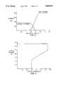
- FIG. 4illustrates how the current limit function of the embodiment in FIG. 2 affects the operation of the voltage regulator as a short-circuit condition is approached at outputs terminal 15.
- the nominal regulated output voltageis 3.3V
- the maximum current limit threshold(when the foldback current is zero and I ref is at its maximum) is chosen to be 650 mA
- the minimum or short-circuit current limit threshold(when I ref is zero and the foldback current is at its maximum) is chosen to be 300 mA.
- other valuesmay be used if desired.
- the current limit function of the voltage regulator of FIG. 2causes the current limit threshold to decrease as the output voltage at output terminal 15 drops below 2.4 V, due to an overload condition present at output terminal 15.
- This first breakpointcorresponds to the progressive decrease of the limit current on line 70 due to the drop in the output voltage.
- a second breakpointis introduced in the curve.
- the limit currentis equal to zero, the start-up current is completely turned on, and a minimum current limit threshold value is established by the foldback current and resistor 325.
- the short-circuit current limit thresholdis less than the current limit threshold at the first breakpoint, and unnecessary power dissipation is prevented.
- the quantity of interest in the current limit signalmay be a voltage, rather than a current as in the embodiment of FIG. 2, where this voltage may be provided directly from voltage reference circuit 180.
- the quantity of interest in the foldback signalmay also be a voltage.
- signal combiner circuit 150would be a voltage summing amplifier.
- the start-up control signal provided by signal generator circuit 47could be a voltage, in which case current shunt circuit 120 could be a FET with its gate responsive to the voltage of the start-up control signal.
Landscapes
- Engineering & Computer Science (AREA)
- Physics & Mathematics (AREA)
- Electromagnetism (AREA)
- General Physics & Mathematics (AREA)
- Radar, Positioning & Navigation (AREA)
- Automation & Control Theory (AREA)
- Continuous-Control Power Sources That Use Transistors (AREA)
Abstract
Description
Claims (24)
Priority Applications (1)
| Application Number | Priority Date | Filing Date | Title |
|---|---|---|---|
| US08/722,342US5666044A (en) | 1995-09-29 | 1996-09-27 | Start up circuit and current-foldback protection for voltage regulators |
Applications Claiming Priority (2)
| Application Number | Priority Date | Filing Date | Title |
|---|---|---|---|
| US462595P | 1995-09-29 | 1995-09-29 | |
| US08/722,342US5666044A (en) | 1995-09-29 | 1996-09-27 | Start up circuit and current-foldback protection for voltage regulators |
Publications (1)
| Publication Number | Publication Date |
|---|---|
| US5666044Atrue US5666044A (en) | 1997-09-09 |
Family
ID=26673257
Family Applications (1)
| Application Number | Title | Priority Date | Filing Date |
|---|---|---|---|
| US08/722,342Expired - LifetimeUS5666044A (en) | 1995-09-29 | 1996-09-27 | Start up circuit and current-foldback protection for voltage regulators |
Country Status (1)
| Country | Link |
|---|---|
| US (1) | US5666044A (en) |
Cited By (47)
| Publication number | Priority date | Publication date | Assignee | Title |
|---|---|---|---|---|
| US5821740A (en)* | 1996-02-15 | 1998-10-13 | Harris Corporation | DC-to-DC converter having fast over-current detection and associated methods |
| US5994884A (en)* | 1998-08-27 | 1999-11-30 | The United States Of America As Represented By The Secretary Of The Navy | Booster circuit for foldback current limited power supplies |
| EP0987615A1 (en)* | 1998-09-16 | 2000-03-22 | Matsushita Electric Industrial Co., Ltd. | Power circuit including inrush current limiter, and integrated circuit including the power circuit |
| EP0968871A3 (en)* | 1998-07-03 | 2000-03-29 | Hitachi, Ltd. | Power-feed control apparatus provided in a vehicle |
| US6163140A (en)* | 2000-02-01 | 2000-12-19 | Micrel Incorporated | Start-up circuit for voltage regulators |
| EP1093044A1 (en)* | 1999-10-13 | 2001-04-18 | Sgs Thomson Microelectronics Sa | Linear regulator with low serial voltage dropout |
| US6285569B1 (en)* | 2000-02-22 | 2001-09-04 | Semiconductor Components Industries Llc | Switched mode power supply controller circuit and method thereof |
| US6373339B2 (en)* | 2000-06-23 | 2002-04-16 | International Business Machines Corporation | Active bias network circuit for radio frequency amplifier |
| US6429631B2 (en)* | 2000-02-29 | 2002-08-06 | Sharp Kabushiki Kaisha | Regulated power source circuit including an overcurrent detecting mechanism for eliminating loss in the output control element |
| US6441594B1 (en)* | 2001-04-27 | 2002-08-27 | Motorola Inc. | Low power voltage regulator with improved on-chip noise isolation |
| US6466422B2 (en) | 2001-01-02 | 2002-10-15 | Shenzhen Sts Microelectronics Co., Ltd. | Current limit protection circuit for a voltage regulator |
| US6483684B2 (en)* | 1999-11-30 | 2002-11-19 | Ando Electric Co., Ltd. | Current limiting apparatus |
| US6518906B2 (en)* | 2000-07-25 | 2003-02-11 | Agere Systems Guardian Corp. | Use of current folding to improve the performance of a current -steered DAC operating at low supply voltage |
| US6525515B1 (en)* | 2001-09-24 | 2003-02-25 | Supertex, Inc. | Feedback apparatus and method for adaptively controlling power supplied to a hot-pluggable subsystem |
| US20030054780A1 (en)* | 2000-09-05 | 2003-03-20 | Hitachi, Ltd. | High frequency power amplifying circuit, and mobile communication apparatus using it |
| US20030224624A1 (en)* | 2002-05-28 | 2003-12-04 | Semiconductor Components Industries,Llc | Method of forming a semiconductor device and structure therefor |
| US6664773B1 (en) | 2002-05-23 | 2003-12-16 | Semiconductor Components Industries Llc | Voltage mode voltage regulator with current mode start-up |
| US6894468B1 (en)* | 1999-07-07 | 2005-05-17 | Synqor, Inc. | Control of DC/DC converters having synchronous rectifiers |
| US20050116692A1 (en)* | 2003-12-02 | 2005-06-02 | Minoru Sugiyama | Method and apparatus for power supplying capable of effectively eliminating overshoot voltage |
| WO2005064239A1 (en) | 2003-12-30 | 2005-07-14 | Nuovo Pignone Holding S.P.A. | Combustion system with low polluting emissions |
| US20050157437A1 (en)* | 2003-11-25 | 2005-07-21 | Katsunori Kimura | Overcurrent protection circuit |
| US20070001657A1 (en)* | 2005-06-30 | 2007-01-04 | Mellachurvu Murthy R | Supply regulator |
| US20070040602A1 (en)* | 2005-08-17 | 2007-02-22 | Chung-Wei Lin | Circuit for reference current and voltage generation |
| US20080030177A1 (en)* | 2006-08-01 | 2008-02-07 | Hung-I Chen | Soft-start circuit of linear voltage regulator and method thereof |
| US20080061752A1 (en)* | 2006-09-13 | 2008-03-13 | Linear Technology Corporation | Programmable constant power foldback |
| US20090021308A1 (en)* | 2007-07-17 | 2009-01-22 | Benjamin Heilmann | Voltage Regulator Startup Method and Apparatus |
| US20090243565A1 (en)* | 2008-03-27 | 2009-10-01 | Microsemi Corp. - Analog Mixed Signal Group, Ltd. | Method and apparatus for detecting end of start up phase |
| US20090309511A1 (en)* | 2008-06-16 | 2009-12-17 | Anthony Mangiaracina | Dimming fluorescent ballast system with shutdown control circuit |
| US20090309562A1 (en)* | 2008-06-12 | 2009-12-17 | Laszlo Lipcsei | Power regulator |
| US20100103707A1 (en)* | 2008-10-27 | 2010-04-29 | Atmel Corporation | Contactless Interface |
| US20100327828A1 (en)* | 2009-06-30 | 2010-12-30 | Green Solution Technology Co., Ltd. | Mosfet current limiting circuit, linear voltage regulator and voltage converting circuit |
| US7969127B1 (en) | 2008-04-25 | 2011-06-28 | National Semiconductor Corporation | Start-up circuit for a shunt regulator |
| EP2450768A1 (en) | 2010-09-20 | 2012-05-09 | Dialog Semiconductor GmbH | Startup circuit for self-supplied voltage regulator |
| US20120187930A1 (en)* | 2011-01-25 | 2012-07-26 | Microchip Technology Incorporated | Voltage regulator having current and voltage foldback based upon load impedance |
| US20130120891A1 (en)* | 2011-11-14 | 2013-05-16 | Texas Instruments Incorporated | Systems and Methods of Over-Load Protection with Voltage Fold-Back |
| US20130270902A1 (en)* | 2012-04-17 | 2013-10-17 | Siemens Aktiengesellschaft | Fault Protection System For A Power System Of Dynamically Positioned Vessel |
| US8674672B1 (en)* | 2011-12-30 | 2014-03-18 | Cypress Semiconductor Corporation | Replica node feedback circuit for regulated power supply |
| EP2677388A3 (en)* | 2012-05-31 | 2014-03-19 | Nxp B.V. | Voltage regulator circuit with adaptive current limit and method for operating the voltage regulator circuit |
| US20140184166A1 (en)* | 2011-06-10 | 2014-07-03 | Keiichiro Ohkawa | Battery control device and battery system |
| US20140184185A1 (en)* | 2013-01-03 | 2014-07-03 | Stmicroelectronics S.R.L. | Electric system comprising a load driving apparatus by auto-recovery mode, and method of operating the apparatus |
| US8847565B2 (en)* | 2012-09-14 | 2014-09-30 | Nxp B.V. | Shunt regulator for adverse voltage/circuit conditions |
| EP2887174A1 (en)* | 2013-12-20 | 2015-06-24 | Dialog Semiconductor GmbH | CC-CV method to control the startup current for LDO |
| US20160268896A1 (en)* | 2015-03-12 | 2016-09-15 | Qualcomm Incorporated | Switched mode power supply having a staircase current limit |
| US9667134B2 (en)* | 2015-09-15 | 2017-05-30 | Texas Instruments Deutschland Gmbh | Startup circuit for reference circuits |
| WO2017201214A1 (en)* | 2016-05-17 | 2017-11-23 | Texas Instruments Incorporated | Generating the under voltage protection threshold |
| US20220035392A1 (en)* | 2020-07-28 | 2022-02-03 | Medtronic Minimed, Inc. | Linear voltage regulator with isolated supply current |
| US11378993B2 (en) | 2020-09-23 | 2022-07-05 | Microsoft Technology Licensing, Llc | Voltage regulator circuit with current limiter stage |
Citations (4)
| Publication number | Priority date | Publication date | Assignee | Title |
|---|---|---|---|---|
| US3753078A (en)* | 1972-05-03 | 1973-08-14 | Gen Electric | Foldback current control circuit |
| US3988643A (en)* | 1974-10-25 | 1976-10-26 | Litton Business Systems, Inc. | Latch circuit |
| US4016461A (en)* | 1976-05-06 | 1977-04-05 | Amp Incorporated | Starting circuit for switching regulator |
| US5592072A (en)* | 1995-01-24 | 1997-01-07 | Dell Usa, L.P. | High performance dual section voltage regulator |
- 1996
- 1996-09-27USUS08/722,342patent/US5666044A/ennot_activeExpired - Lifetime
Patent Citations (4)
| Publication number | Priority date | Publication date | Assignee | Title |
|---|---|---|---|---|
| US3753078A (en)* | 1972-05-03 | 1973-08-14 | Gen Electric | Foldback current control circuit |
| US3988643A (en)* | 1974-10-25 | 1976-10-26 | Litton Business Systems, Inc. | Latch circuit |
| US4016461A (en)* | 1976-05-06 | 1977-04-05 | Amp Incorporated | Starting circuit for switching regulator |
| US5592072A (en)* | 1995-01-24 | 1997-01-07 | Dell Usa, L.P. | High performance dual section voltage regulator |
Cited By (84)
| Publication number | Priority date | Publication date | Assignee | Title |
|---|---|---|---|---|
| US5821740A (en)* | 1996-02-15 | 1998-10-13 | Harris Corporation | DC-to-DC converter having fast over-current detection and associated methods |
| US6320275B1 (en) | 1998-07-03 | 2001-11-20 | Hitachi, Ltd. | Power-feed control apparatus provided in a vehicle |
| EP0968871A3 (en)* | 1998-07-03 | 2000-03-29 | Hitachi, Ltd. | Power-feed control apparatus provided in a vehicle |
| US5994884A (en)* | 1998-08-27 | 1999-11-30 | The United States Of America As Represented By The Secretary Of The Navy | Booster circuit for foldback current limited power supplies |
| US6150800A (en)* | 1998-09-16 | 2000-11-21 | Matsushita Electric Industrial Co., Ltd. | Power circuit including inrush current limiter, and integrated circuit including the power circuit |
| EP0987615A1 (en)* | 1998-09-16 | 2000-03-22 | Matsushita Electric Industrial Co., Ltd. | Power circuit including inrush current limiter, and integrated circuit including the power circuit |
| US6894468B1 (en)* | 1999-07-07 | 2005-05-17 | Synqor, Inc. | Control of DC/DC converters having synchronous rectifiers |
| US7119524B2 (en) | 1999-07-07 | 2006-10-10 | Bank America, N.A. | Control of DC/DC converters having synchronous rectifiers |
| US6445167B1 (en) | 1999-10-13 | 2002-09-03 | Stmicroelectronics S.A. | Linear regulator with a low series voltage drop |
| EP1093044A1 (en)* | 1999-10-13 | 2001-04-18 | Sgs Thomson Microelectronics Sa | Linear regulator with low serial voltage dropout |
| FR2799849A1 (en)* | 1999-10-13 | 2001-04-20 | St Microelectronics Sa | LINEAR REGULATOR WITH LOW VOLTAGE DROP SERIES |
| US6483684B2 (en)* | 1999-11-30 | 2002-11-19 | Ando Electric Co., Ltd. | Current limiting apparatus |
| US6163140A (en)* | 2000-02-01 | 2000-12-19 | Micrel Incorporated | Start-up circuit for voltage regulators |
| US6285569B1 (en)* | 2000-02-22 | 2001-09-04 | Semiconductor Components Industries Llc | Switched mode power supply controller circuit and method thereof |
| US6429631B2 (en)* | 2000-02-29 | 2002-08-06 | Sharp Kabushiki Kaisha | Regulated power source circuit including an overcurrent detecting mechanism for eliminating loss in the output control element |
| US6373339B2 (en)* | 2000-06-23 | 2002-04-16 | International Business Machines Corporation | Active bias network circuit for radio frequency amplifier |
| US6518906B2 (en)* | 2000-07-25 | 2003-02-11 | Agere Systems Guardian Corp. | Use of current folding to improve the performance of a current -steered DAC operating at low supply voltage |
| US20030054780A1 (en)* | 2000-09-05 | 2003-03-20 | Hitachi, Ltd. | High frequency power amplifying circuit, and mobile communication apparatus using it |
| US6466422B2 (en) | 2001-01-02 | 2002-10-15 | Shenzhen Sts Microelectronics Co., Ltd. | Current limit protection circuit for a voltage regulator |
| WO2002088863A1 (en)* | 2001-04-27 | 2002-11-07 | Motorola, Inc. | Low power voltage regulator with improved on-chip noise isolation |
| US6441594B1 (en)* | 2001-04-27 | 2002-08-27 | Motorola Inc. | Low power voltage regulator with improved on-chip noise isolation |
| US6525515B1 (en)* | 2001-09-24 | 2003-02-25 | Supertex, Inc. | Feedback apparatus and method for adaptively controlling power supplied to a hot-pluggable subsystem |
| US6664773B1 (en) | 2002-05-23 | 2003-12-16 | Semiconductor Components Industries Llc | Voltage mode voltage regulator with current mode start-up |
| US6791390B2 (en) | 2002-05-28 | 2004-09-14 | Semiconductor Components Industries, L.L.C. | Method of forming a voltage regulator semiconductor device having feedback and structure therefor |
| US20030224624A1 (en)* | 2002-05-28 | 2003-12-04 | Semiconductor Components Industries,Llc | Method of forming a semiconductor device and structure therefor |
| US7289308B2 (en)* | 2003-11-25 | 2007-10-30 | Seiko Instruments Inc. | Overcurrent protection circuit |
| US20050157437A1 (en)* | 2003-11-25 | 2005-07-21 | Katsunori Kimura | Overcurrent protection circuit |
| US7638987B2 (en)* | 2003-12-02 | 2009-12-29 | Ricoh Company, Ltd. | Method and apparatus for power supplying capable of effectively eliminating overshoot voltage |
| US20050116692A1 (en)* | 2003-12-02 | 2005-06-02 | Minoru Sugiyama | Method and apparatus for power supplying capable of effectively eliminating overshoot voltage |
| WO2005064239A1 (en) | 2003-12-30 | 2005-07-14 | Nuovo Pignone Holding S.P.A. | Combustion system with low polluting emissions |
| US20070001657A1 (en)* | 2005-06-30 | 2007-01-04 | Mellachurvu Murthy R | Supply regulator |
| US7557550B2 (en)* | 2005-06-30 | 2009-07-07 | Silicon Laboratories Inc. | Supply regulator using an output voltage and a stored energy source to generate a reference signal |
| US20070040602A1 (en)* | 2005-08-17 | 2007-02-22 | Chung-Wei Lin | Circuit for reference current and voltage generation |
| US7436244B2 (en)* | 2005-08-17 | 2008-10-14 | Industrial Technology Research Institute | Circuit for reference current and voltage generation |
| US20080030177A1 (en)* | 2006-08-01 | 2008-02-07 | Hung-I Chen | Soft-start circuit of linear voltage regulator and method thereof |
| US20080061752A1 (en)* | 2006-09-13 | 2008-03-13 | Linear Technology Corporation | Programmable constant power foldback |
| US7538528B2 (en)* | 2006-09-13 | 2009-05-26 | Linear Technology Corporation | Constant power foldback mechanism programmable to approximate safe operating area of pass device for providing connection to load |
| US20090021308A1 (en)* | 2007-07-17 | 2009-01-22 | Benjamin Heilmann | Voltage Regulator Startup Method and Apparatus |
| US7855542B2 (en)* | 2007-07-17 | 2010-12-21 | Qimonda Ag | Voltage regulator startup method and apparatus |
| US20090243565A1 (en)* | 2008-03-27 | 2009-10-01 | Microsemi Corp. - Analog Mixed Signal Group, Ltd. | Method and apparatus for detecting end of start up phase |
| US8149602B2 (en)* | 2008-03-27 | 2012-04-03 | Microsemi Corp.-Analog Mixed Signal Group, Ltd. | Method and apparatus for detecting end of start up phase |
| US7969127B1 (en) | 2008-04-25 | 2011-06-28 | National Semiconductor Corporation | Start-up circuit for a shunt regulator |
| US8570013B2 (en) | 2008-06-12 | 2013-10-29 | O2Micro, Inc. | Power regulator for converting an input voltage to an output voltage |
| US20090309562A1 (en)* | 2008-06-12 | 2009-12-17 | Laszlo Lipcsei | Power regulator |
| US8143872B2 (en)* | 2008-06-12 | 2012-03-27 | O2Micro, Inc | Power regulator |
| WO2010005608A1 (en)* | 2008-06-16 | 2010-01-14 | Nextek Power Systems, Inc. | Dimming fluorescent ballast system with shutdown control circuit |
| US8022639B2 (en) | 2008-06-16 | 2011-09-20 | Nextek Power Systems, Inc. | Dimming fluorescent ballast system with shutdown control circuit |
| US20090309511A1 (en)* | 2008-06-16 | 2009-12-17 | Anthony Mangiaracina | Dimming fluorescent ballast system with shutdown control circuit |
| US8611119B2 (en) | 2008-10-27 | 2013-12-17 | Inside Contactless S.A. | Contactless interface |
| CN102203806A (en)* | 2008-10-27 | 2011-09-28 | 英赛瑟库尔公司 | Contactless interface |
| US20100103707A1 (en)* | 2008-10-27 | 2010-04-29 | Atmel Corporation | Contactless Interface |
| CN102203806B (en)* | 2008-10-27 | 2015-04-15 | 英赛瑟库尔公司 | Contactless interface |
| US20100327828A1 (en)* | 2009-06-30 | 2010-12-30 | Green Solution Technology Co., Ltd. | Mosfet current limiting circuit, linear voltage regulator and voltage converting circuit |
| TWI420277B (en)* | 2009-06-30 | 2013-12-21 | Green Solution Tech Co Ltd | Mosfet current limiting circuit and voltage converter using the same |
| EP2450768A1 (en) | 2010-09-20 | 2012-05-09 | Dialog Semiconductor GmbH | Startup circuit for self-supplied voltage regulator |
| US8400124B2 (en) | 2010-09-20 | 2013-03-19 | Dialog Semiconductor Gmbh | Startup circuit for self-supplied voltage regulator |
| CN103392159B (en)* | 2011-01-25 | 2016-11-23 | 密克罗奇普技术公司 | There is electric current based on load impedance and the voltage regulator of voltage foldback |
| US8841897B2 (en)* | 2011-01-25 | 2014-09-23 | Microchip Technology Incorporated | Voltage regulator having current and voltage foldback based upon load impedance |
| CN103392159A (en)* | 2011-01-25 | 2013-11-13 | 密克罗奇普技术公司 | Voltage regulator having current and voltage foldback based upon load impedance |
| US20120187930A1 (en)* | 2011-01-25 | 2012-07-26 | Microchip Technology Incorporated | Voltage regulator having current and voltage foldback based upon load impedance |
| TWI547783B (en)* | 2011-01-25 | 2016-09-01 | 微晶片科技公司 | Voltage regulator having current and voltage foldback based upon load impedance |
| US9641011B2 (en)* | 2011-06-10 | 2017-05-02 | Hitachi Automotive Systems, Ltd. | Battery control device adapting the battery current limit by decreasing the stored current limit by comparing it with the measured battery current |
| US20140184166A1 (en)* | 2011-06-10 | 2014-07-03 | Keiichiro Ohkawa | Battery control device and battery system |
| US20130120891A1 (en)* | 2011-11-14 | 2013-05-16 | Texas Instruments Incorporated | Systems and Methods of Over-Load Protection with Voltage Fold-Back |
| US9680365B2 (en)* | 2011-11-14 | 2017-06-13 | Texas Insturments Incorporated | Systems and methods of over-load protection with voltage fold-back |
| US8674672B1 (en)* | 2011-12-30 | 2014-03-18 | Cypress Semiconductor Corporation | Replica node feedback circuit for regulated power supply |
| US20130270902A1 (en)* | 2012-04-17 | 2013-10-17 | Siemens Aktiengesellschaft | Fault Protection System For A Power System Of Dynamically Positioned Vessel |
| US9543748B2 (en)* | 2012-04-17 | 2017-01-10 | Siemens Aktiengesellschaft | Fault protection system for a power system of dynamically positioned vessel |
| US9075422B2 (en) | 2012-05-31 | 2015-07-07 | Nxp B.V. | Voltage regulator circuit with adaptive current limit and method for operating the voltage regulator circuit |
| EP2677388A3 (en)* | 2012-05-31 | 2014-03-19 | Nxp B.V. | Voltage regulator circuit with adaptive current limit and method for operating the voltage regulator circuit |
| US8847565B2 (en)* | 2012-09-14 | 2014-09-30 | Nxp B.V. | Shunt regulator for adverse voltage/circuit conditions |
| US20140184185A1 (en)* | 2013-01-03 | 2014-07-03 | Stmicroelectronics S.R.L. | Electric system comprising a load driving apparatus by auto-recovery mode, and method of operating the apparatus |
| US9436193B2 (en)* | 2013-01-03 | 2016-09-06 | Stmicroelectronics S.R.L. | Electric system comprising a load driving apparatus by auto-recovery mode, and method of operating the apparatus |
| US20150177757A1 (en)* | 2013-12-20 | 2015-06-25 | Dialog Semiconductor Gmbh | CC-CV Method to Control the Startup Current for LDO |
| US9170594B2 (en)* | 2013-12-20 | 2015-10-27 | Dialog Semiconductor Gmbh | CC-CV method to control the startup current for LDO |
| EP2887174A1 (en)* | 2013-12-20 | 2015-06-24 | Dialog Semiconductor GmbH | CC-CV method to control the startup current for LDO |
| US20160268896A1 (en)* | 2015-03-12 | 2016-09-15 | Qualcomm Incorporated | Switched mode power supply having a staircase current limit |
| US10027225B2 (en)* | 2015-03-12 | 2018-07-17 | Qualcomm Incorporated | Switched mode power supply having a staircase current limit |
| US9667134B2 (en)* | 2015-09-15 | 2017-05-30 | Texas Instruments Deutschland Gmbh | Startup circuit for reference circuits |
| WO2017201214A1 (en)* | 2016-05-17 | 2017-11-23 | Texas Instruments Incorporated | Generating the under voltage protection threshold |
| US20220035392A1 (en)* | 2020-07-28 | 2022-02-03 | Medtronic Minimed, Inc. | Linear voltage regulator with isolated supply current |
| US11960311B2 (en)* | 2020-07-28 | 2024-04-16 | Medtronic Minimed, Inc. | Linear voltage regulator with isolated supply current |
| US12405624B2 (en) | 2020-07-28 | 2025-09-02 | Medtronic Minimed, Inc. | Linear voltage regulator and test system |
| US11378993B2 (en) | 2020-09-23 | 2022-07-05 | Microsoft Technology Licensing, Llc | Voltage regulator circuit with current limiter stage |
Similar Documents
| Publication | Publication Date | Title |
|---|---|---|
| US5666044A (en) | Start up circuit and current-foldback protection for voltage regulators | |
| US5570060A (en) | Circuit for limiting the current in a power transistor | |
| US7151365B2 (en) | Constant voltage generator and electronic equipment using the same | |
| JP2689708B2 (en) | Bias current control circuit | |
| US5552697A (en) | Low voltage dropout circuit with compensating capacitance circuitry | |
| US5563501A (en) | Low voltage dropout circuit with compensating capacitance circuitry | |
| US5939867A (en) | Low consumption linear voltage regulator with high supply line rejection | |
| US5274323A (en) | Control circuit for low dropout regulator | |
| KR101071799B1 (en) | Constant voltage circuit and method of controlling output voltage of constant voltage circuit | |
| US6819165B2 (en) | Voltage regulator with dynamically boosted bias current | |
| US5625278A (en) | Ultra-low drop-out monolithic voltage regulator | |
| US5548205A (en) | Method and circuit for control of saturation current in voltage regulators | |
| US6559626B2 (en) | Voltage regulator | |
| US6441594B1 (en) | Low power voltage regulator with improved on-chip noise isolation | |
| US7615977B2 (en) | Linear voltage regulator and method of limiting the current in such a regulator | |
| EP0846996B1 (en) | Power transistor control circuit for a voltage regulator | |
| US5410241A (en) | Circuit to reduce dropout voltage in a low dropout voltage regulator using a dynamically controlled sat catcher | |
| US20040046532A1 (en) | Low dropout voltage regulator using a depletion pass transistor | |
| US5929616A (en) | Device for voltage regulation with a low internal dissipation of energy | |
| JPH10133754A (en) | Regulator circuit and semiconductor integrated circuit device | |
| EP0967538B1 (en) | Output control circuit for a voltage regulator | |
| US20220229455A1 (en) | Low-power voltage regulator with fast transient response | |
| US6310467B1 (en) | LDO regulator with thermal shutdown system and method | |
| US7049799B2 (en) | Voltage regulator and electronic device | |
| CN111488028A (en) | Method of forming semiconductor device |
Legal Events
| Date | Code | Title | Description |
|---|---|---|---|
| AS | Assignment | Owner name:CHERRY SEMICONDUCTOR CORPORATION, RHODE ISLAND Free format text:ASSIGNMENT OF ASSIGNORS INTEREST;ASSIGNOR:TUOZZOLO, CLAUDIO;REEL/FRAME:008322/0556 Effective date:19961030 | |
| STCF | Information on status: patent grant | Free format text:PATENTED CASE | |
| FEPP | Fee payment procedure | Free format text:PAYOR NUMBER ASSIGNED (ORIGINAL EVENT CODE: ASPN); ENTITY STATUS OF PATENT OWNER: LARGE ENTITY | |
| AS | Assignment | Owner name:CHASE MANHATTAN BANK, THE, NEW YORK Free format text:SECURITY INTEREST;ASSIGNOR:SEMICONDUCTOR COMPONENTS INDUSTRIES OF RHODE ISLAND, INC.;REEL/FRAME:010785/0094 Effective date:20000403 | |
| AS | Assignment | Owner name:SEMICONDUCTOR COMPONENTS INDUSTRIES OF RHODE ISLAN Free format text:CHANGE OF NAME;ASSIGNOR:CHERRY SEMICONDUCTOR CORPORATION, A RHODE ISLAND CORPORATION;REEL/FRAME:011044/0427 Effective date:20000403 | |
| FPAY | Fee payment | Year of fee payment:4 | |
| AS | Assignment | Owner name:JPMORGAN CHASE BANK, AS COLLATERAL AGENT, NEW YORK Free format text:SUPPLEMENT TO SECURITY AGREEMENT;ASSIGNORS:SEMICONDUCTOR COMPONENTS INDUSTRIES, LLC;SEMICONDUCTOR COMPONENTS OF RHODE ISLAND, INC.;REEL/FRAME:012991/0180 Effective date:20020505 | |
| AS | Assignment | Owner name:WELLS FARGO BANK MINNESOTA, NATIONAL ASSOCIATION, Free format text:SECURITY AGREEMENT;ASSIGNORS:SEMICONDUCTOR COMPONENTS INDUSTRIES, LLC;SEMICONDUCTOR COMPONENTS INDUSTRIES OF RHODE ISLAND, INC.;REEL/FRAME:012958/0638 Effective date:20020506 | |
| AS | Assignment | Owner name:JPMORGAN CHASE BANK, NEW YORK Free format text:SECURITY INTEREST;ASSIGNOR:SEMICONDUCTOR COMPONENTS INDUSTRIES, LLC;REEL/FRAME:014007/0239 Effective date:20030303 | |
| FPAY | Fee payment | Year of fee payment:8 | |
| FPAY | Fee payment | Year of fee payment:12 | |
| AS | Assignment | Owner name:SEMICONDUCTOR COMPONENTS INDUSTRIES, LLC, ARIZONA Free format text:ASSIGNMENT OF ASSIGNORS INTEREST;ASSIGNOR:SEMICONDUCTOR COMPONENTS INDUSTRIES OF RHODE ISLAND, INC.;REEL/FRAME:034021/0452 Effective date:20141023 | |
| AS | Assignment | Owner name:DEUTSCHE BANK AG NEW YORK BRANCH, NEW YORK Free format text:SECURITY INTEREST;ASSIGNOR:SEMICONDUCTOR COMPONENTS INDUSTRIES, LLC;REEL/FRAME:038620/0087 Effective date:20160415 | |
| AS | Assignment | Owner name:SEMICONDUCTOR COMPONENTS INDUSTRIES, LLC, ARIZONA Free format text:RELEASE BY SECURED PARTY;ASSIGNOR:WELLS FARGO BANK MINNESOTA, NATIONAL ASSOCIATION, AS COLLATERAL AGENT;REEL/FRAME:038543/0039 Effective date:20050217 | |
| AS | Assignment | Owner name:SEMICONDUCTOR COMPONENTS INDUSTRIES, LLC, ARIZONA Free format text:RELEASE BY SECURED PARTY;ASSIGNOR:JPMORGAN CHASE BANK, N.A., AS ADMINISTRATIVE AGENT AND COLLATERAL AGENT;REEL/FRAME:038631/0345 Effective date:20100511 Owner name:SEMICONDUCTOR COMPONENTS INDUSTRIES, LLC, ARIZONA Free format text:RELEASE BY SECURED PARTY;ASSIGNOR:JPMORGAN CHASE BANK, N.A. (ON ITS BEHALF AND ON BEHALF OF ITS PREDECESSOR IN INTEREST, CHASE MANHATTAN BANK);REEL/FRAME:038632/0074 Effective date:20160415 | |
| AS | Assignment | Owner name:DEUTSCHE BANK AG NEW YORK BRANCH, AS COLLATERAL AG Free format text:CORRECTIVE ASSIGNMENT TO CORRECT THE INCORRECT PATENT NUMBER 5859768 AND TO RECITE COLLATERAL AGENT ROLE OF RECEIVING PARTY IN THE SECURITY INTEREST PREVIOUSLY RECORDED ON REEL 038620 FRAME 0087. ASSIGNOR(S) HEREBY CONFIRMS THE SECURITY INTEREST;ASSIGNOR:SEMICONDUCTOR COMPONENTS INDUSTRIES, LLC;REEL/FRAME:039853/0001 Effective date:20160415 Owner name:DEUTSCHE BANK AG NEW YORK BRANCH, AS COLLATERAL AGENT, NEW YORK Free format text:CORRECTIVE ASSIGNMENT TO CORRECT THE INCORRECT PATENT NUMBER 5859768 AND TO RECITE COLLATERAL AGENT ROLE OF RECEIVING PARTY IN THE SECURITY INTEREST PREVIOUSLY RECORDED ON REEL 038620 FRAME 0087. ASSIGNOR(S) HEREBY CONFIRMS THE SECURITY INTEREST;ASSIGNOR:SEMICONDUCTOR COMPONENTS INDUSTRIES, LLC;REEL/FRAME:039853/0001 Effective date:20160415 | |
| AS | Assignment | Owner name:FAIRCHILD SEMICONDUCTOR CORPORATION, ARIZONA Free format text:RELEASE OF SECURITY INTEREST IN PATENTS RECORDED AT REEL 038620, FRAME 0087;ASSIGNOR:DEUTSCHE BANK AG NEW YORK BRANCH, AS COLLATERAL AGENT;REEL/FRAME:064070/0001 Effective date:20230622 Owner name:SEMICONDUCTOR COMPONENTS INDUSTRIES, LLC, ARIZONA Free format text:RELEASE OF SECURITY INTEREST IN PATENTS RECORDED AT REEL 038620, FRAME 0087;ASSIGNOR:DEUTSCHE BANK AG NEW YORK BRANCH, AS COLLATERAL AGENT;REEL/FRAME:064070/0001 Effective date:20230622 |