US5665249A - Micro-electromechanical die module with planarized thick film layer - Google Patents
Micro-electromechanical die module with planarized thick film layerDownload PDFInfo
- Publication number
- US5665249A US5665249AUS08/330,146US33014694AUS5665249AUS 5665249 AUS5665249 AUS 5665249AUS 33014694 AUS33014694 AUS 33014694AUS 5665249 AUS5665249 AUS 5665249A
- Authority
- US
- United States
- Prior art keywords
- thick film
- polyimide
- substrate
- patterned
- film layer
- Prior art date
- Legal status (The legal status is an assumption and is not a legal conclusion. Google has not performed a legal analysis and makes no representation as to the accuracy of the status listed.)
- Expired - Lifetime
Links
- 229920001721polyimidePolymers0.000claimsabstractdescription128
- 239000004642PolyimideSubstances0.000claimsabstractdescription127
- 239000000758substrateSubstances0.000claimsabstractdescription54
- 230000015572biosynthetic processEffects0.000claimsabstractdescription39
- 238000005755formation reactionMethods0.000claimsabstractdescription39
- 238000000059patterningMethods0.000claimsabstractdescription8
- 238000005498polishingMethods0.000claimsdescription68
- 238000010438heat treatmentMethods0.000claimsdescription50
- 239000011324beadSubstances0.000claimsdescription33
- 239000002002slurrySubstances0.000claimsdescription30
- 238000000034methodMethods0.000claimsdescription28
- 238000004519manufacturing processMethods0.000claimsdescription27
- XUIMIQQOPSSXEZ-UHFFFAOYSA-NSiliconChemical compound[Si]XUIMIQQOPSSXEZ-UHFFFAOYSA-N0.000claimsdescription13
- 239000010703siliconSubstances0.000claimsdescription13
- 229910052710siliconInorganic materials0.000claimsdescription13
- 230000004888barrier functionEffects0.000claimsdescription9
- 238000004528spin coatingMethods0.000claimsdescription8
- 238000003491arrayMethods0.000claimsdescription6
- 238000000151depositionMethods0.000claimsdescription5
- 238000005520cutting processMethods0.000claims1
- 238000006073displacement reactionMethods0.000claims1
- 239000000463materialSubstances0.000abstractdescription16
- 230000008021depositionEffects0.000abstractdescription4
- 235000012431wafersNutrition0.000description128
- 239000010410layerSubstances0.000description119
- 239000000976inkSubstances0.000description63
- 230000008569processEffects0.000description14
- 238000012876topographyMethods0.000description11
- 239000000853adhesiveSubstances0.000description9
- 230000001070adhesive effectEffects0.000description9
- 229910052751metalInorganic materials0.000description9
- 239000002184metalSubstances0.000description8
- 238000007517polishing processMethods0.000description8
- 239000000243solutionSubstances0.000description8
- VYPSYNLAJGMNEJ-UHFFFAOYSA-NSilicium dioxideChemical compoundO=[Si]=OVYPSYNLAJGMNEJ-UHFFFAOYSA-N0.000description7
- 239000007788liquidSubstances0.000description7
- 239000012790adhesive layerSubstances0.000description6
- 230000006872improvementEffects0.000description5
- 238000007639printingMethods0.000description5
- 229910052715tantalumInorganic materials0.000description5
- GUVRBAGPIYLISA-UHFFFAOYSA-Ntantalum atomChemical compound[Ta]GUVRBAGPIYLISA-UHFFFAOYSA-N0.000description5
- 229910052581Si3N4Inorganic materials0.000description4
- 230000000694effectsEffects0.000description4
- 230000013011matingEffects0.000description4
- 238000002161passivationMethods0.000description4
- 238000000926separation methodMethods0.000description4
- HQVNEWCFYHHQES-UHFFFAOYSA-Nsilicon nitrideChemical compoundN12[Si]34N5[Si]62N3[Si]51N64HQVNEWCFYHHQES-UHFFFAOYSA-N0.000description4
- BNGXYYYYKUGPPF-UHFFFAOYSA-M(3-methylphenyl)methyl-triphenylphosphanium;chlorideChemical compound[Cl-].CC1=CC=CC(C[P+](C=2C=CC=CC=2)(C=2C=CC=CC=2)C=2C=CC=CC=2)=C1BNGXYYYYKUGPPF-UHFFFAOYSA-M0.000description3
- 229910052782aluminiumInorganic materials0.000description3
- XAGFODPZIPBFFR-UHFFFAOYSA-NaluminiumChemical compound[Al]XAGFODPZIPBFFR-UHFFFAOYSA-N0.000description3
- 238000005336crackingMethods0.000description3
- 239000013078crystalSubstances0.000description3
- 239000003989dielectric materialSubstances0.000description3
- 238000005516engineering processMethods0.000description3
- 238000005530etchingMethods0.000description3
- -1for exampleSubstances0.000description3
- 239000011521glassSubstances0.000description3
- TWNQGVIAIRXVLR-UHFFFAOYSA-Noxo(oxoalumanyloxy)alumaneChemical compoundO=[Al]O[Al]=OTWNQGVIAIRXVLR-UHFFFAOYSA-N0.000description3
- 239000011241protective layerSubstances0.000description3
- 239000000377silicon dioxideSubstances0.000description3
- 235000012239silicon dioxideNutrition0.000description3
- 238000011144upstream manufacturingMethods0.000description3
- XLYOFNOQVPJJNP-UHFFFAOYSA-NwaterSubstancesOXLYOFNOQVPJJNP-UHFFFAOYSA-N0.000description3
- 230000009471actionEffects0.000description2
- 238000003486chemical etchingMethods0.000description2
- 239000011248coating agentSubstances0.000description2
- 238000000576coating methodMethods0.000description2
- 239000010438graniteSubstances0.000description2
- 239000011810insulating materialSubstances0.000description2
- 230000005499meniscusEffects0.000description2
- 238000012986modificationMethods0.000description2
- 230000004048modificationEffects0.000description2
- 239000002245particleSubstances0.000description2
- 230000002265preventionEffects0.000description2
- 238000007665saggingMethods0.000description2
- 239000004065semiconductorSubstances0.000description2
- 239000000126substanceSubstances0.000description2
- VHUUQVKOLVNVRT-UHFFFAOYSA-NAmmonium hydroxideChemical compound[NH4+].[OH-]VHUUQVKOLVNVRT-UHFFFAOYSA-N0.000description1
- JOYRKODLDBILNP-UHFFFAOYSA-NEthyl urethaneChemical compoundCCOC(N)=OJOYRKODLDBILNP-UHFFFAOYSA-N0.000description1
- ZLMJMSJWJFRBEC-UHFFFAOYSA-NPotassiumChemical compound[K]ZLMJMSJWJFRBEC-UHFFFAOYSA-N0.000description1
- 238000005299abrasionMethods0.000description1
- 239000003929acidic solutionSubstances0.000description1
- 230000002378acidificating effectEffects0.000description1
- 239000000908ammonium hydroxideSubstances0.000description1
- 238000013459approachMethods0.000description1
- 239000006227byproductSubstances0.000description1
- 230000008859changeEffects0.000description1
- BGTFCAQCKWKTRL-YDEUACAXSA-Nchembl1095986Chemical compoundC1[C@@H](N)[C@@H](O)[C@H](C)O[C@H]1O[C@@H]([C@H]1C(N[C@H](C2=CC(O)=CC(O[C@@H]3[C@H]([C@@H](O)[C@H](O)[C@@H](CO)O3)O)=C2C=2C(O)=CC=C(C=2)[C@@H](NC(=O)[C@@H]2NC(=O)[C@@H]3C=4C=C(C(=C(O)C=4)C)OC=4C(O)=CC=C(C=4)[C@@H](N)C(=O)N[C@@H](C(=O)N3)[C@H](O)C=3C=CC(O4)=CC=3)C(=O)N1)C(O)=O)=O)C(C=C1)=CC=C1OC1=C(O[C@@H]3[C@H]([C@H](O)[C@@H](O)[C@H](CO[C@@H]5[C@H]([C@@H](O)[C@H](O)[C@@H](C)O5)O)O3)O[C@@H]3[C@H]([C@@H](O)[C@H](O)[C@@H](CO)O3)O[C@@H]3[C@H]([C@H](O)[C@@H](CO)O3)O)C4=CC2=C1BGTFCAQCKWKTRL-YDEUACAXSA-N0.000description1
- 239000007795chemical reaction productSubstances0.000description1
- 239000008119colloidal silicaSubstances0.000description1
- 238000004891communicationMethods0.000description1
- 239000002131composite materialSubstances0.000description1
- 238000013329compoundingMethods0.000description1
- 150000001875compoundsChemical class0.000description1
- 230000001010compromised effectEffects0.000description1
- 238000005260corrosionMethods0.000description1
- 230000007797corrosionEffects0.000description1
- 239000006184cosolventSubstances0.000description1
- 230000001351cycling effectEffects0.000description1
- 230000002939deleterious effectEffects0.000description1
- 230000001419dependent effectEffects0.000description1
- 230000001627detrimental effectEffects0.000description1
- 229910003460diamondInorganic materials0.000description1
- 239000010432diamondSubstances0.000description1
- 239000000945fillerSubstances0.000description1
- 238000010304firingMethods0.000description1
- 239000012530fluidSubstances0.000description1
- 210000000497foam cellAnatomy0.000description1
- 230000037406food intakeEffects0.000description1
- 238000009472formulationMethods0.000description1
- 238000007641inkjet printingMethods0.000description1
- 239000012212insulatorSubstances0.000description1
- 150000002500ionsChemical class0.000description1
- 238000003475laminationMethods0.000description1
- 238000010297mechanical methods and processMethods0.000description1
- 230000005226mechanical processes and functionsEffects0.000description1
- 239000007769metal materialSubstances0.000description1
- 150000002739metalsChemical class0.000description1
- 238000004377microelectronicMethods0.000description1
- 239000000203mixtureSubstances0.000description1
- 230000003287optical effectEffects0.000description1
- 239000012044organic layerSubstances0.000description1
- 230000010355oscillationEffects0.000description1
- 230000003534oscillatory effectEffects0.000description1
- 230000002093peripheral effectEffects0.000description1
- 238000000206photolithographyMethods0.000description1
- 229920000728polyesterPolymers0.000description1
- 239000013047polymeric layerSubstances0.000description1
- 239000004814polyurethaneSubstances0.000description1
- 229920002635polyurethanePolymers0.000description1
- 239000011148porous materialSubstances0.000description1
- 229910052700potassiumInorganic materials0.000description1
- KWYUFKZDYYNOTN-UHFFFAOYSA-Mpotassium hydroxideSubstances[OH-].[K+]KWYUFKZDYYNOTN-UHFFFAOYSA-M0.000description1
- 230000000135prohibitive effectEffects0.000description1
- 230000001737promoting effectEffects0.000description1
- 230000009467reductionEffects0.000description1
- 230000001172regenerating effectEffects0.000description1
- 238000012216screeningMethods0.000description1
- 238000007789sealingMethods0.000description1
- 239000011856silicon-based particleSubstances0.000description1
- 239000007787solidSubstances0.000description1
- 238000009987spinningMethods0.000description1
- 238000005507sprayingMethods0.000description1
- 238000003892spreadingMethods0.000description1
- 230000007480spreadingEffects0.000description1
- 239000007858starting materialSubstances0.000description1
Images


Classifications
- B—PERFORMING OPERATIONS; TRANSPORTING
- B41—PRINTING; LINING MACHINES; TYPEWRITERS; STAMPS
- B41J—TYPEWRITERS; SELECTIVE PRINTING MECHANISMS, i.e. MECHANISMS PRINTING OTHERWISE THAN FROM A FORME; CORRECTION OF TYPOGRAPHICAL ERRORS
- B41J2/00—Typewriters or selective printing mechanisms characterised by the printing or marking process for which they are designed
- B41J2/005—Typewriters or selective printing mechanisms characterised by the printing or marking process for which they are designed characterised by bringing liquid or particles selectively into contact with a printing material
- B41J2/01—Ink jet
- B41J2/135—Nozzles
- B41J2/16—Production of nozzles
- B41J2/1621—Manufacturing processes
- B41J2/1623—Manufacturing processes bonding and adhesion
- B—PERFORMING OPERATIONS; TRANSPORTING
- B24—GRINDING; POLISHING
- B24B—MACHINES, DEVICES, OR PROCESSES FOR GRINDING OR POLISHING; DRESSING OR CONDITIONING OF ABRADING SURFACES; FEEDING OF GRINDING, POLISHING, OR LAPPING AGENTS
- B24B37/00—Lapping machines or devices; Accessories
- B24B37/04—Lapping machines or devices; Accessories designed for working plane surfaces
- B—PERFORMING OPERATIONS; TRANSPORTING
- B41—PRINTING; LINING MACHINES; TYPEWRITERS; STAMPS
- B41J—TYPEWRITERS; SELECTIVE PRINTING MECHANISMS, i.e. MECHANISMS PRINTING OTHERWISE THAN FROM A FORME; CORRECTION OF TYPOGRAPHICAL ERRORS
- B41J2/00—Typewriters or selective printing mechanisms characterised by the printing or marking process for which they are designed
- B41J2/005—Typewriters or selective printing mechanisms characterised by the printing or marking process for which they are designed characterised by bringing liquid or particles selectively into contact with a printing material
- B41J2/01—Ink jet
- B41J2/135—Nozzles
- B41J2/16—Production of nozzles
- B41J2/1601—Production of bubble jet print heads
- B41J2/1604—Production of bubble jet print heads of the edge shooter type
- B—PERFORMING OPERATIONS; TRANSPORTING
- B41—PRINTING; LINING MACHINES; TYPEWRITERS; STAMPS
- B41J—TYPEWRITERS; SELECTIVE PRINTING MECHANISMS, i.e. MECHANISMS PRINTING OTHERWISE THAN FROM A FORME; CORRECTION OF TYPOGRAPHICAL ERRORS
- B41J2/00—Typewriters or selective printing mechanisms characterised by the printing or marking process for which they are designed
- B41J2/005—Typewriters or selective printing mechanisms characterised by the printing or marking process for which they are designed characterised by bringing liquid or particles selectively into contact with a printing material
- B41J2/01—Ink jet
- B41J2/135—Nozzles
- B41J2/16—Production of nozzles
- B41J2/1621—Manufacturing processes
- B41J2/1626—Manufacturing processes etching
- B—PERFORMING OPERATIONS; TRANSPORTING
- B41—PRINTING; LINING MACHINES; TYPEWRITERS; STAMPS
- B41J—TYPEWRITERS; SELECTIVE PRINTING MECHANISMS, i.e. MECHANISMS PRINTING OTHERWISE THAN FROM A FORME; CORRECTION OF TYPOGRAPHICAL ERRORS
- B41J2/00—Typewriters or selective printing mechanisms characterised by the printing or marking process for which they are designed
- B41J2/005—Typewriters or selective printing mechanisms characterised by the printing or marking process for which they are designed characterised by bringing liquid or particles selectively into contact with a printing material
- B41J2/01—Ink jet
- B41J2/135—Nozzles
- B41J2/16—Production of nozzles
- B41J2/1621—Manufacturing processes
- B41J2/1631—Manufacturing processes photolithography
- B—PERFORMING OPERATIONS; TRANSPORTING
- B41—PRINTING; LINING MACHINES; TYPEWRITERS; STAMPS
- B41J—TYPEWRITERS; SELECTIVE PRINTING MECHANISMS, i.e. MECHANISMS PRINTING OTHERWISE THAN FROM A FORME; CORRECTION OF TYPOGRAPHICAL ERRORS
- B41J2/00—Typewriters or selective printing mechanisms characterised by the printing or marking process for which they are designed
- B41J2/005—Typewriters or selective printing mechanisms characterised by the printing or marking process for which they are designed characterised by bringing liquid or particles selectively into contact with a printing material
- B41J2/01—Ink jet
- B41J2/135—Nozzles
- B41J2/16—Production of nozzles
- B41J2/1621—Manufacturing processes
- B41J2/1632—Manufacturing processes machining
- B—PERFORMING OPERATIONS; TRANSPORTING
- B41—PRINTING; LINING MACHINES; TYPEWRITERS; STAMPS
- B41J—TYPEWRITERS; SELECTIVE PRINTING MECHANISMS, i.e. MECHANISMS PRINTING OTHERWISE THAN FROM A FORME; CORRECTION OF TYPOGRAPHICAL ERRORS
- B41J2/00—Typewriters or selective printing mechanisms characterised by the printing or marking process for which they are designed
- B41J2/005—Typewriters or selective printing mechanisms characterised by the printing or marking process for which they are designed characterised by bringing liquid or particles selectively into contact with a printing material
- B41J2/01—Ink jet
- B41J2/135—Nozzles
- B41J2/16—Production of nozzles
- B41J2/1621—Manufacturing processes
- B41J2/1635—Manufacturing processes dividing the wafer into individual chips
- B—PERFORMING OPERATIONS; TRANSPORTING
- B41—PRINTING; LINING MACHINES; TYPEWRITERS; STAMPS
- B41J—TYPEWRITERS; SELECTIVE PRINTING MECHANISMS, i.e. MECHANISMS PRINTING OTHERWISE THAN FROM A FORME; CORRECTION OF TYPOGRAPHICAL ERRORS
- B41J2/00—Typewriters or selective printing mechanisms characterised by the printing or marking process for which they are designed
- B41J2/005—Typewriters or selective printing mechanisms characterised by the printing or marking process for which they are designed characterised by bringing liquid or particles selectively into contact with a printing material
- B41J2/01—Ink jet
- B41J2/135—Nozzles
- B41J2/16—Production of nozzles
- B41J2/1621—Manufacturing processes
- B41J2/164—Manufacturing processes thin film formation
- B41J2/1642—Manufacturing processes thin film formation thin film formation by CVD [chemical vapor deposition]
- B—PERFORMING OPERATIONS; TRANSPORTING
- B41—PRINTING; LINING MACHINES; TYPEWRITERS; STAMPS
- B41J—TYPEWRITERS; SELECTIVE PRINTING MECHANISMS, i.e. MECHANISMS PRINTING OTHERWISE THAN FROM A FORME; CORRECTION OF TYPOGRAPHICAL ERRORS
- B41J2/00—Typewriters or selective printing mechanisms characterised by the printing or marking process for which they are designed
- B41J2/005—Typewriters or selective printing mechanisms characterised by the printing or marking process for which they are designed characterised by bringing liquid or particles selectively into contact with a printing material
- B41J2/01—Ink jet
- B41J2/135—Nozzles
- B41J2/16—Production of nozzles
- B41J2/1621—Manufacturing processes
- B41J2/164—Manufacturing processes thin film formation
- B41J2/1645—Manufacturing processes thin film formation thin film formation by spincoating
- B—PERFORMING OPERATIONS; TRANSPORTING
- B41—PRINTING; LINING MACHINES; TYPEWRITERS; STAMPS
- B41J—TYPEWRITERS; SELECTIVE PRINTING MECHANISMS, i.e. MECHANISMS PRINTING OTHERWISE THAN FROM A FORME; CORRECTION OF TYPOGRAPHICAL ERRORS
- B41J2202/00—Embodiments of or processes related to ink-jet or thermal heads
- B41J2202/01—Embodiments of or processes related to ink-jet heads
- B41J2202/03—Specific materials used
- Y—GENERAL TAGGING OF NEW TECHNOLOGICAL DEVELOPMENTS; GENERAL TAGGING OF CROSS-SECTIONAL TECHNOLOGIES SPANNING OVER SEVERAL SECTIONS OF THE IPC; TECHNICAL SUBJECTS COVERED BY FORMER USPC CROSS-REFERENCE ART COLLECTIONS [XRACs] AND DIGESTS
- Y10—TECHNICAL SUBJECTS COVERED BY FORMER USPC
- Y10T—TECHNICAL SUBJECTS COVERED BY FORMER US CLASSIFICATION
- Y10T29/00—Metal working
- Y10T29/49—Method of mechanical manufacture
- Y10T29/49401—Fluid pattern dispersing device making, e.g., ink jet
Definitions
- the present inventionrelates to micro-electromechanical die modules of the type having a planarized, patterned thick film layer sandwiched between silicon substrates, and more particularly to an improved thermal ink jet die module for use as a printhead and method of manufacture therefor, the die module eliminating the effects of standoff between two bonded parts thereof caused by topographic formations formed in a thick film insulating layer sandwiched between said two parts during deposition and patterning thereof.
- the ink jet die moduleis a specific example of a general class of micro-electromechanical die modules which combine electrical and mechanical functionality in an integrated device.
- an ink jet printheadexpels ink droplets on demand by the selective application of a current pulse to a thermal energy generator, usually a resistor, located in capillary-filled, parallel ink channels a predetermined distance upstream from the channel nozzles or orifices.
- a thermal energy generatorusually a resistor, located in capillary-filled, parallel ink channels a predetermined distance upstream from the channel nozzles or orifices.
- U.S. Pat. No. Re. 32,572 to Hawkins et al.exemplifies such a thermal ink jet printhead and several fabricating processes therefor. Each printhead is composed of two parts aligned and bonded together.
- One partis a substantially flat substrate which contains on the surface thereof a linear array of heating elements and addressing electrodes (heater plate), and the second part is a substrate having at least one recess anisotropically etched therein to serve as an ink supply reservoir when the two parts are bonded together (channel plate).
- a linear array of parallel groovesare also formed in the second part, so that one end of the grooves communicate with the reservoir recess and the other ends are open for use as ink droplet expelling nozzles.
- Many printheadscan be made simultaneously by producing a plurality of sets of heating element arrays with their addressing elements on a silicon wafer and by mating a second silicon wafer having a corresponding plurality of sets of channel grooves and associated manifolds therein. After the two wafers are aligned and bonded together, the mated wafers are diced into many separate printheads.
- thermal ink jet printheadsinclude U.S. Pat. No. 4,638,337 to Torpey et al., that discloses an improved printhead similar to that of Hawkins et al., but has each of its heating elements located in a recess (termed heater pit).
- the recess walls containing the heating elementsprevent lateral movement of the bubbles through the nozzle and, therefore, the sudden release of vaporized ink to the atmosphere, known as blow-out, which causes ingestion of air and interrupts the printhead operation.
- a thick film insulative layersuch as polyimide, Riston® or Vacrel® is formed on the wafer containing the heating elements and patterned to provide the recesses for the heating elements, so that the thick film layer is interposed between the two wafers when they are mated together.
- U.S. Pat. No. 4,774,530 to Hawkinsfurther refines the two-part printhead by disclosing an improvement over the patent to Torpey et al.
- further recessesare patterned in the thick film layer to provide a flow path for the ink from the manifold to the channels by enabling the ink to flow around the closed ends of the channels, thereby eliminating the fabrication steps required to open the groove closed ends to the manifold recess.
- the heater plateshaving the aforementioned improvements of heater pits and bypass pits formed in the thick film insulative layer covering the heater plate surface, are aligned with and bonded to the channel plate, so that each channel groove has a recessed heating element therein and a bypass pit to provide an ink passage from the ink manifold to the channel groove.
- U.S. Pat. No. 4,678,529 to Drake et al.discloses a method of bonding ink jet printhead components together by spin coating or spraying a relatively thin, uniform layer of adhesive on a flexible substrate and then manually placing the flexible substrate surface with the adhesive layer against the channel wafer surface having the etched sets of channel grooves and associated manifolds or reservoirs. A uniform pressure and temperature is applied to ensure adhesive contact with all coplanar surface portions and then the flexible substrate peeled away, leaving a uniformly thin coating on the channel wafer surface to be bonded to the heater wafer.
- two wafersare bonded together after alignment for subsequent dicing into individual printheads.
- Each printhead partis formed individually on two separate substrates or wafers, where one contains heating elements and the other ink channels or passageways.
- the wafer containing the ink channelsis silicon, and the channels are formed by an anisotropic etching process.
- the anisotropic or orientation dependent etchinghas been shown to be a high yielding process that produces very planar and highly precise channel plates.
- the other wafer containing the heating elements as well as heater addressing logicis covered by a thick film insulating layer in which heater and bypass pits are formed using photolithography.
- the thick film-layeris preferably polyimide, because it can be patterned in the geometries required, can withstand the temperature cycling of the heater, and is chemically resistant to the ink.
- polyimide materialis its tendency to form unwanted topographical formations, such as raised edges or lips (1-8 microns high) at photoimaged edges.
- each printheadis composed of parts aligned and bonded together.
- One partis a substantially flat substrate which contains on the surface thereof a linear array of heating elements and addressing electrodes (heater plate).
- This parthas a thick film insulative material deposited on the surface with the heating elements and addressing electrodes, and the thick film layer is photolithographically patterned to form ink flow paths, each containing a one of the heating elements, from an ink inlet.
- This inletis usually provided through the flat substrate or heater plate to the heating elements.
- This patterned thick film layeris usually referred to as a "barrier layer".
- the final partis a nozzle plate containing an array of nozzles.
- the nozzle plateis aligned and bonded to the patterned barrier layer, so that each nozzle is aligned directly over one of the heating elements for droplet ejection through the nozzles in a direction perpendicular to the heating element.
- the roofshooter type thermal ink jet printheadis also concerned with topographic formation in the surface of the patterned barrier layer which would prevent adequate bonding of the nozzle plate thereto.
- Polyimide topographysuch as raised edges or lips, are undesirable byproducts resulting from photoimaged and cured heater pits and bypass pits or trenches on heater plates.
- the raised edgesare polyimide topographical features that are formed at the edge of photoimaged areas that do not shrink during curing as would the generally non-patterned larger areas of the polyimide. Consequently, raised edges critically interfere with both the mating and bonding of the heater and channel plates of edge shooter type printheads and the mating and bonding of the heater and nozzle plates of the roofshooter printheads.
- edge beads or raised areas at the edge of the waferAnother form of polyimide topography is encountered in the form of edge beads or raised areas at the edge of the wafer, when a layer of liquid polyimide is dispensed and spun onto a wafer.
- centripetal forcespush the spinning liquid polyimide towards the outside of the wafer to form an edge bead.
- the edge bead on a 4 inch diameter waferfor example, is on the order of 3 mm-15 mm wide radially from the outer edge thereof.
- the periphery of the wafersis not completely circular.
- the thickness of the edge beadvaries from a few micrometers thicker than the rest of the polyimide layer to twice as thick as the majority center portion. Due to the asymmetry of the periphery of the wafer caused by the flats, the thickness of the edge bead varies substantially around the edge of each wafer. Such edge beads of polyimide prevent adequate bonding between the wafers.
- Edge beadscan also cause a reduction in yield, because the additional stress placed on the center area of the channel plate during heater and channel plated bonding may cause cracking. Edge beads, if removed from the edge of the heater wafers, cantilevers the channel plate at its outside edges and can again cause cracks to be formed in the outer peripheral area of the channel wafer. Such cracking in the channel wafer will degrade the reliability of the individual printheads after they have separated from the wafer pair.
- Raised edges and edge beadsare not the only topographical formation created from photoimaged polyimide.
- Other topographical formationssuch as wall sags or dips, compound the negative effects of raised edges by adding to the standoff between the bonded heater and channel plates.
- Wall dipsare slumps in the polyimide walls between closely adjacent polyimide photoimaged pits.
- the polyimide layer sandwiched between the two wafersgenerally has a thickness of 10 to 40 ⁇ m (cured) and can form more than 2 microns of topographical variation.
- the bonding adhesiveis approximately 2 microns or less thick which does not allow the adhesive to bridge or fill in the formation of inter-channel gaps caused by the topographic formations.
- a final cause of polyimide surface topographyresults from the presence of topography associated with the microelectronic device fabrication prior to spin casting the polyimide.
- Spin castingtends to cause the polyimide to conform and replicate features present on the wafer's surface. Since the surface contains features up to 4 ⁇ m thick, the polyimide surface varies by a similar amount. It is important to point out that even if no polyimide was present, it would still be difficult to completely bond a channel wafer to a heater wafer. In this content it is desirable to add an intermediate polyimide layer, if its surface can subsequently be planarized, after first being patterned to expose critical device structures. In the more general case of microelectromechanical die modules, the polyimide layer or other suitable organic layer can be added solely for this purpose.
- the fabrication sequencecompensates for the raised edges by including a non-functional straddling channel that nullifies the standoff created by the raised edge and a corresponding additional non-functional pit that positions the raised edge away from the functional channels and nozzles.
- this fabrication techniquecompensates for polyimide raised edges, it does not attempt to solve the problem of edge bead or dips between channels.
- the slurrytypically consists of fumed silicon particles in an alkaline medium such as potassium or ammonium hydroxide.
- the polishing padis generally made of cast or sliced polyurethane with a filler of urethane coated polyester felt. Pores in the pad surface aid in slurry transport, and the polymeric foam cell walls of the pad, in combination with the slurry particles, remove the reaction products from the wafer surface. Glazing of the pad's surface is thought to be the reason for the pad's drop in efficiency and removal rate over time. This means the pad surface must be reconditioned after every run by abrading its surface with, for example, a diamond wheel, thereby regenerating the surface rather than removing material from the pad.
- the primary focus for chemical-mechanical polishingis to planarize continuous surfaces such as oxide passivation layers and continuous surfaces containing both oxides and metals.
- the present inventionis concerned with obtaining a planarized polyimide layer which has a discontinuous surface; i.e., one having recesses therein.
- CMPchemical-mechanical polishing
- Japanese Laid-Open No. 3-268392discloses a manufacturing method for a multilayer interconnection or wiring board.
- a first wiring patternis formed on an insulating substrate, together with cylindrical electroconductive columns connected thereto.
- the first wiring pattern and electroconductive columnsare covered by an insulating layer.
- the surface of insulating layeris polished to planarize the insulating layer surface and to expose the electroconductive columns by a scanning polishing jig which has a polishing area smaller than 30% of the area of the wiring pattern.
- a second wiring patternis formed on the flat insulating layer surface and connected to the exposed electroconductive columns.
- U.S. Pat. No. 4,944,836 to Beyer et al.discloses a method for producing coplanar metal/insulator films on a substrate by chemical-mechanical polishing.
- a substrate having an insulating layer of dielectric material thereonis patterned to produce recesses therein and then the patterned insulating layer is coated with a layer of metal.
- the substrateis placed in a polisher and the metal is removed everywhere except in the recesses. This is made possible by the use of a selective slurry which removes the metal much faster than the dielectric material, thereby producing a continuous coplanar surface of metal and insulating material.
- a substrate having a patterned metallic layeris coated with an insulating layer and then subjected to chemical-mechanical polishing.
- the structureis coplanarized by the chemical-mechanical removal of the insulating material at a significantly higher rate than the underlying metal to be exposed at the termination of the polishing.
- the polishing padis firm enough so that it does not deform under the polishing load.
- patterned polymeric materialsuch as, for example, polyimide
- a micro-electromechanical devicesuch as an ink jet printhead
- MEMSmicro-electromechanical systems
- Such MEMS devicesgenerally have two silicon wafers or substrates bonded together by an intermediate, patterned thick film polymeric layer, such as, for example, polyimide.
- the patterned features in the thick film layerprovide cavities for the housing of electrical and electromechanical devices, such as, pressure sensors, accelerometers, and the like and including liquid flow structures and passageways that are hermetically sealed between the two silicon wafers. Planarizing the thick film layer to remove protruding topographic formations caused, for example, by the patterning process results in a stronger bond between the wafers, as well as better seals between the wafers and the thick film layer with the patterned recesses.
- a MEMS deviceis an ink jet die module which may be either an "edge shooter” or “roof shooter” type thermal ink jet printhead.
- the heater plateIn a roof shooter type printhead, the heater plate has an array of heating elements with addressing electrodes and an opening therethrough for use as an ink inlet.
- a barrier layer of photopatternable materialis deposited over the heating elements and addressing electrodes and then patterned to define liquid (ink) flow directing passageways. Each passageway contains a heating element and is in communication with the ink inlet.
- a nozzle plate containing an array of nozzles or orificeis aligned and bonded to the patterned barrier layer, so that one nozzle is positioned directly over a heating element for droplet ejection therethrough in a direction perpendicular to the heating element.
- a heater platehas an array of heating elements and addressing electrodes on one surface thereof, and a thick film layer is deposited over this surface and the heating elements. The thick film layer is patterned to expose the heating elements in pits and provide bypass pits for the passageway of ink.
- a channel plateis etched to form, in one surface thereof, an array of parallel channels having open ends for nozzles and closed ends adjacent an ink reservoir with an ink inlet.
- the channel plateis aligned and bonded to the patterned thick film layer.
- Each channelhas at least one heating element located a predetermined distance from the channel open ends or nozzles, which are located along one edge, generally referenced to as a nozzle face. Droplets of ink are ejected through the nozzles in a direction parallel to the surface of the heating elements.
- the patterning of the thick film layer of a MEMS devicecauses protruding topographic formations such as raised lips or sagging walls referred to as dips.
- the thick film layeris applied to one of the substrates of the die module (e.g., a heater plate or heater wafer) by spin coating, an edge bead is formed at the periphery of the substrate. If the substrate does not have a circular shape, for example, a wafer with flats (removed chordal sections) for subsequent in identifying wafer type, crystal plane orientation, and use as alignment edges, the edge bead will vary in thickness around the periphery. These topographic formations are detrimental to all micro-electromechanical systems (MEMS).
- MEMSmicro-electromechanical systems
- the present inventionis a MEMS device having a planarized intermediate patterned thick film layer and-method of achieving the planarization.
- the heater and channel wafer standoff by topographic formationsis eliminated by planarization of the polyimide layer by a predetermined chemical-mechanical polishing process after it is patterned and cured and prior to its alignment and bonding to the channel wafer. Because the curing of the polyimide increases the topographic variation, prior art printheads used only partially cured polyimide which was not as robust and resistant to attack by a wider range of inks as a fully cured polyimide.
- the method of fabricating an edge shooter type ink jet printhead having a substrate, such as a silicon wafer, containing a plurality of heating elements and driver circuitry on one surface thereof which are covered by a thick film insulative layer having recesses patterned therein,comprises the following steps:
- a thick film insulative layersuch as polyimide
- the thick filmcan be deposited by spin coating from the liquid state or lamination from the solid state.
- the thick film layer of polyimideis patterned and cured to provide a predetermined number of recesses with substantially vertical walls at predetermined locations in the outer surface of the thick film layer.
- the recess wallsintersect the thick film outer surface to define an edge around each recess, where unwanted topographic formations are formed.
- a chemical-mechanical polishing processis performed on the outer surface of the patterned thick film layer to remove the topographic formations and thereby planarize the thick film outer surface without rounding off the recess edges, so that the raised ridges and other unwanted topographic formations are removed at a faster rate than the remainder of the outer surface of the thick film layer.
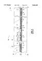
- FIG. 1is an enlarged cross-sectional view of a portion of a typical prior art bonded channel wafer and heater plates.
- FIG. 2is an enlarged view of the area identified in FIG. 1 by circle 2.
- FIG. 3is an enlarged cross-sectional view of a portion of a typical prior art bonded wafer pair.
- FIG. 4is a cross-sectional front view of a portion of an aligned and adhesively bonded channel wafer and heater wafer formed in accordance with the present invention.
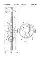
- FIG. 5is an enlarged view of the area identified in FIG. 3 by circle 5.
- FIG. 6is an enlarged, schematic cross-sectional view of a single printhead after being severed from the aligned and bonded wafer pair in FIG. 4.
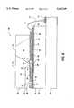
- FIG. 7is a schematically shown, partially sectioned, side elevation view of a chemical-mechanical polishing device having a rotatable vacuum chuck holding a wafer with a thick film layer to be planarized against a rotatable pad with a polishing slurry thereon.
- FIG. 8is a schematic plan view of the rotatable pad and rotatable vacuum chucks of FIG. 7, showing the relative movements of the chucks and pad with the polishing slurry omitted.
- the present inventionis described using an ink jet die module or printhead as a typical MEMS device.
- An edge shooter configuration for the die modulehas been arbitrarily selected, but the planarization of the ink flow directing barrier layer of a roof shooter type die module is achieved in the same way.
- FIG. 1shows a cross-sectional view of wafer pair 54 with the cross-section being perpendicular to the channels 20
- FIG. 3shows a cross-sectional view of the wafer pair with the cross-section being taken parallel to and through one of the channels 20.
- FIG. 2is an enlarged view of the area circled in FIG. 1 identified by circle 2.
- a thick film layer 18 of photopatternable materialsuch as polyimide
- a thick film layer 18 of photopatternable materialis deposited over the surface of a silicon substrate or wafer 49 having a plurality of linear arrays of heating elements 34 with protective layer 17, usually tantalum, and driver/logic circuitry (not shown) for each heating element array formed on an underglaze layer 39, such as silicon nitride or silicon dioxide, which thermally isolates the heating elements from the silicon wafer.
- the circuitry, including electrodes 33, (FIG. 3)is passivated by a layer 45 of silicon nitride or CVD silicon dioxide prior to the deposition of the polyimide.
- Topographic formations 40, 41are formed when heater pits 26 are photolithographically processed in a thick film insulating layer 18, such as polyimide, on heater wafer 49. These formations on the outer opposing pits in the array have the negative quality of increasing the standoff between channel wafer 47 and heater wafer 49.
- One topographic formation formed while curing the photoimaged polyimideis raised edge or lip 40 which attributes to heater and channel plate standoff as indicated by spacing 42 in FIG. 2.
- Raised edge 40is formed in polyimide thick film layer 18 on the outer sides of the outer heater pits 26 and outer sides of the bypass pits 38, (see FIG. 3), as well as in the front and back of each of the heater and bypass pits.
- Lips 40are formed on any edge of a large area of polyimide, such as for recesses 55 formed for die cuts 48 shown in FIGS. 1 and 3.
- the channel plate standoff caused by the lips formed to the front and back of the pitshas less effect because the channels 20 and reservoirs 24 straddle them, but the lips on the sides of pits 26 and recesses 55 produce the substantial separation or standoff.
- a second topographic formationis a sag or dip in wall 15 between the pits as indicated by spacing 41 in FIGS. 1 and 2. Sag is caused by the narrow width of polyimide between recesses, such as that formed between the closely spaced heater pits and bypass pits.
- a third topographic formationis edge bead 73.
- This topographic formationis not a function of the photopatterning process for polyimides, but rather a function of centripetal forces incurred while spin forming the fluid polyimide layer 18 on the heater wafer 49.
- the edge bead 73is held on the wafer by surface tension.
- the polyimideis applied to the wafer 49 as a viscous liquid and spun to cover the wafer.
- the width and height of the edge beadis determined by the spin parameters, shape of the wafer (flats and locations), and thickness of the film.
- the width of the edge bead 73is on the order of 3 mm, as indicated by the distance 75, and the thickness of the edge bead is about 32 ⁇ m in some locations as indicated by the dimension 74.
- chordal portions of a circular wafer, such as wafer 49are removed to form straight edge flats (not shown), the periphery of the wafer is no longer circular, so that the edge bead 73 formed varies in thickness, compounding the problem of planarization.
- the flatsare necessary for identification of wafer type, location of crystal planes, and for use in assembly operation for alignment purposes.
- the patterning or etching of recesses in a single polyimide layersuch as, for example, heater and bypass pits of FIGS. 1-3, cause raised lips or edges at the edges of the recesses, whenever the recess edge was adjacent a relatively large area of unpatterned polyimide layer.
- the polyimide wallwould sag.
- the walls of polyimide between the heater and bypass pitswould generally sag, while the upstream and downstream edges of the pits relative to the subsequent nozzle location would develop raised lips.
- the outer edges of the outer pits in each array of heater and bypass pitsdeveloped raised lips.
- the pits 26 for the outer heating element in each array and the outer bypass pit 38have raised edges of 1 to 8 ⁇ m, when the polyimide is in the 35 to 50 ⁇ m thickness range, the minimum thickness required for the prevention of lateral movement of the droplet ejecting bubbles for printing at 300 spots per inch (spi).
- the upstream and downstream ends of the prior art pits relative to the subsequent nozzle locationalso have raised edges, but these raised edges generally do not interfere with bonding of the channel and heater wafers because the channels straddle the heater pits and the raised edges on the downstream ends of the bypass pits.
- the other ends of the bypass pitsare in the large reservoir recess 24 with the open bottom 25 for ink inlet.
- the polyimide layer 18is spin coated over the heating element arrays and their associated driver/logic circuitry.
- thermal ink jet die or printheads 10(FIG. 6) of the present invention are generated in batches by aligning and adhesively bonding an anisotropically etched channel wafer 47 to a heater wafer 49 (FIG. 4) followed by a dicing step to separate the bonded wafers into individual printheads 10.
- an underglaze layer 39is formed thereon, such as, silicon dioxide or silicon nitride.
- a protection layer for the heating elementsis formed with a layer of tantalum, electrically insulated from the heater surface with silicon nitride.
- addressing electrodes 33are formed.
- a passivation layer 45 for the electrodes and active circuitryis deposited and patterned away from the heating elements 34 and contact pads 32 (see FIG. 6). It can consist of PSG, Si x N y , polyimide, or a composite thereof.
- each heating element 34is 4 wt. % PSG, covered by 3-4 microns of polyimide. It provides an ion barrier to protect exposed electrodes from the ink.
- a layer of thick-film, polymeric, insulative material 18, such as, polyimideis spin deposited on surface 30 of the heater wafer 49 and over the passivated heating element, driver circuitry, and electrodes.
- the thick filmhas a thickness of 15 to 65 ⁇ m, which will cure to a thickness of 10 to 35 microns except for the edge bead 73, as discussed earlier with respect to FIGS. 1 and 3.
- a primary function of the thick filmis to contain the expanding vapor bubble following pulsing of the heater to eject an ink droplet. Consequently, the thickness of the thick film layer 18 is determined by the size of the drop required. For 300 spi, the optimal thickness is about 35 microns.
- the polyimide layer 18is patterned to remove the polyimide over the heating elements (forming pits 26), bypass pits 38, and recesses 55 for dicing cuts, and then cured.
- Fully cured polyimideis known to be much more resistant to chemical attack by more aggressive inks which have high pH and contain aggressive cosolvents. Unfortunately, fully curing of the patterned polyimide layer 18 causes the unwanted topographic formations, such as raised lips, to increase in height. Therefore, the patterned polyimide layers could not be fully cured before planarization was made practical.
- a heater waferis mounted on each of the two rotatable, circular vacuum chucks 53 of a partially shown, chemical-mechanical polishing device 52, as shown in FIG. 7.
- the surface of the heater wafer 49, opposite the one with the polyimide layer,is gripped by a vacuum force from a vacuum pump (not shown) connected to small openings 64 in the vacuum chuck.
- a vacuum pumpnot shown
- the patterned polyimide layer 18is faced downward confronting a circular polishing pad 56 mounted on a rotatable table 66 located in an open cylindrical chamber 57 formed by chamber wall 58 and chamber floor 59.
- a liquid polishing solution or slurry 50is dispensed from tube 65 onto a rotatable granite polishing table 66 covered with a polishing pad 56.
- the slurryis dispensed through tube 65 from a slurry supply tank (not shown) onto the pad of the pad, as the pad and a table are rotated by a motor (not shown) about axis shaft 63.
- the polishing solution or slurry 50is provided from the supply tank by a pump (not shown) within the chemical-mechanical polishing device.
- the polishing solution or slurry of aluminum oxide and aluminum nitrateis available from Rodel as R90 slurry which is diluted with water 10:1 by volume.
- the average aluminum oxide particle size 0.8-1.4 microns and the water soluble aluminum nitrateprovides a slightly acidic slurry.
- the slurryis used at room temperature.
- the wafersare mounted in the vacuum chucks 53 and the vacuum chucks are swivelly mounted on rotatable spindles 60 in the chemical-mechanical polishing device with polyimide layer 18 face down.
- the spindlesare lowered and the polyimide layer on the wafers brought down onto the rotating pad 56 covered granite table.
- the padis coated with slurry which is dispensed from tube 65 and flows across it, with a pressure of from 0.5 to 10 psi.
- a backpressurecan be applied simultaneously with the downforce by drawing vacuum on the wafer.
- the backpressure by the vacuumshapes the wafer to be concave.
- the vacuum backpressure on the wafercan vary from 0-15 psi.
- the backpressureis 10 psi with a spindle applied downforce of 2 psi.
- the downforce on the heater waferis preferably 4 psi.
- the table 66can rotate between 10 and 250 RPM.
- the spindlescan rotate between 10 and 250 RPM in a direction with, as well as opposite to, that of the table. As shown in FIG.
- the spindlescan oscillate with a stroke of 0-6 inches at a frequency from 0 to 20 cycles per minute (cpm), thus moving the polyimide layer against the slurry covered pad 56 in an oscillatory, back-and-forth direction other as indicated by arrows 81, while concurrently being rotated as indicated by arrows 51.
- the preferred table speedis 100 RPM and the spindle speed is 125 RPM in the same rotary direction with a 1 inch oscillation at 6 cpm, during the planarization by the chemical-mechanical polishing procedure.
- the flow of the slurryis maintained across the interface between the surface of the polyimide layer and the polishing pad by the continual dispensing thereof from the tube 65, the oscillating and rotary movement of the vacuum chucks and the rotary movement of the polishing pad.
- a pattern of circular recesses or dimples 68 in the surface of the polishing padalso assists in maintaining a relatively uniform layer of slurry between the polyimide layer on the wafer and the polishing pad surface 69.
- the slurry flow rateis preferably 400 ml/min.
- the raised surface of the polyimide layer in contact with the polishing padis removed at a faster rate than the surface portions that are in contact only with the polishing solution.
- Uniform pressure of the polishing pad against the polyimide layercauses the polishing accomplished by the combination of polishing solution and polishing pad to remove the unwanted topographical formations (i.e., raised lips and edge bead) without wearing or rounding the edges of the heater pits and bypass pits.
- the heater waferhas uneven topography because of the patterned polyimide layer.
- the uneven heater wafer surfacecomes from both the multiple layers (field oxide, Al metal, passivation, PSG flow glass) which are used to create the circuitry and, more importantly, from curing of the final polyimide layer, which is about 35 ⁇ m thick.
- the edgesdevelop "lips" or ridges following curing.
- Polyimideis a very rigid material after it is fully cured. The high areas prevent good sealing between the low areas of the heater wafer and the channel wafer and the resulting die module produced poor print quality.
- One known process which was used for die modules which printed at 300 spiwas to optimize the polyimide cure cycle so that the material was not fully cured. Not fully curing the polyimide was necessary because, as polyimide becomes more fully cured, the topographic formations become more severe; i.e., the lip height grows. Therefore, the degree of cure of the polyimide layer was compromised to achieve acceptable topography. When the polishing process above is used, the patterned polyimide may be fully cured.
- the spin casting of polyimidecreates an edge bead 73 around the periphery of the heater wafer 49 which is nonuniform in thickness, because of the flats diced on the wafer, and can be twice as high as the central portion of the polyimide layer's surface (70 ⁇ m thick).
- application of pressuretends to crack the channel wafer even before the wafer surfaces contact each other during the mating and bonding step.
- One prior art process usedis to chemically remove the polyimide around the edge of the wafer. Although this enables the wafers to be bonded, yield loss occurs because the heater wafer edge and the channel wafer edge extend beyond the sandwiched polyimide layer, forming cantilevered edges, and cracking occurs around the edge of the channel wafer during bonding.
- the preferred solution to the heater wafer topography problemis to planarize the surface of the heater wafer after the polyimide layer is applied and patterned.
- typical polishing techniquesincluding known chemical-mechanical polishing, eliminated the lips, but polished the edges of the heater and bypass pits more rapidly than the bulk surface, creating dips between the heaters, made the wafers' thickness nonuniform in bulk or non-patterned areas of the polyimide layer, although they started out uniformly thick, tore off pieces of the polyimide walls between the pits, and could not completely remove the relatively large edge bead.
- the present invention for polishing polyimideis only a mechanical process.
- the etch rateis slow and nonuniform.
- the slurry that was found to produce satisfactory results for polyimideis a lightly acidic solution of aluminum oxide, aluminum nitrate, and water, as discussed above, and consequently no chemical etching occurs.
- Typical pressures for chemical-mechanical polishing, as well as conventional glass polishing processes,are at least 7 psi. When a pressure this high was used for patterned polyimide layers on heater wafers, the edge bead was not removed and the bulk non-patterned areas of polyimide becomes nonuniform.
- a key challenge to polishing patterned polyimide layers with an edge beadis that the edge bead thickness is nonuniform because of the wafer flats, and in some places along the edge bead, it is twice as thick as the bulk non-patterned areas.
- the amount of polyimide thickness to be removed from the other patterned structuresis approximately an order of magnitude less. Because of the topography of the patterned polyimide layer with the nonuniform height of the edge bead, the wafer is nonparallel to the polishing table, during at least the initial polishing procedure. At conventional polishing pressures, the wafer deforms enough and bulges from the vacuum chuck to polish in the center simultaneously with polishing at the edge.
- the edge beadBecause the thickness of the edge bead is much greater than in the center, too much material is removed from the center, the edge is not planarized, and some of the edge bead remains. From this result, a low pressure, i.e. ⁇ 2 psi and a hard polishing pad was tried, but the low pressures resulted in severe wall 15 damage between the pits 26. Thus, the optimal pressures were found to vary with the pattern of the polyimide film on the wafer, and in the preferred embodiment for a die module printing at 300 spi, the downward pressure was established as indicated above.
- FIG. 4is a cross-sectional front view of a portion of an aligned and adhesively bonded channel wafer 47 and heater wafer 49 prior to separation into a plurality of individual thermal ink jet printheads 10, shown in FIG. 6.
- FIG. 5is an enlarged cross-sectional view of one of the channels 20 in FIG. 4 and identified by circle 5.
- FIG. 5shows the outer edge of the heater pit 26 after the planarization of the polyimide layer 18 and bonding of the two wafers.
- the interface between the planarized polyimide layer and the channel waferare in full contact, the usual topographic formations of lip 40 and sag 43 having been polished away.
- FIG. 2for comparison.
- the FIG. 4not only are the edge beads and raised lips of FIG. 1 removed by the planarization of the photopatternable, thick film layer, preferably polyimide, but enough of the polyimide layer is removed to eliminate the sag 43 in the walls 15 of polyimide between heater pits 26 and dips due to underlying topography, not planarized by the polyimide.
- the channel wafer surface between channels 20 and the polyimide walls 15 between heater pits 26are in full contact (the adhesive layer not being shown for clarity), as depicted at the interface indicated by index numeral 44.
- FIG. 6a cross-sectional view taken along the length of the channel 20 of printhead 10, incorporating the present invention and showing the front face 29 thereof containing droplet emitting nozzles 27.
- Ink(not shown) flows from the manifold or reservoir 24 and around the end 21 of the groove or ink channel 20, as depicted by arrow 23.
- the lower electrically insulating substrate or heating element plate 28has the heating elements or resistors 34, driver circuitry 36, and addressing elements 33 produced monolithically on underglaze insulating layer 39 formed on surface 30 thereof, while the upper substrate or channel plate 31 has parallel grooves 20 which extend in one direction and penetrate through the channel plate front face 29.
- the end of grooves 20 opposite the nozzlesterminate at slanted wall 21.
- the through recess 24is used as the ink supply manifold for the capillary filled ink channels 20 and has an open bottom 25 for use an as ink fill hole.
- the surface of the channel plate with the groovesare aligned and bonded to the heater plate 28, so that a respective one of the plurality of heating elements 34 is positioned in each channel 20, formed by the grooves and the lower substrate or heater plate.
- the heating elementsare covered by protective layer 17, such as tantalum (Ta), to prevent cavitational damage to the heating elements caused by the collapsing vapor bubbles.
- the printheadscan be mounted on daughterboards 19 and electrically connected to electrodes 12 thereon by wire bonds 14 between the daughterboard electrodes 12 and the contact pads 32 of the printhead.
- the daughterboardprovides the interface with the printer controller (not shown) and power supplies (not shown).
- the patterned polyimide layer 18provides heater pits 26 and ink flow bypass pits 38. The planarization of the patterned polyimide layer 18 eliminates the unwanted topographic formations, so that the channel plate surface between channels 20 and the polyimide walls 15 between the heater pits and bypass pits have full contact (the bonding adhesive is omitted in FIG. 6 for clarity).
Landscapes
- Engineering & Computer Science (AREA)
- Manufacturing & Machinery (AREA)
- Mechanical Engineering (AREA)
- Particle Formation And Scattering Control In Inkjet Printers (AREA)
Abstract
Description
Claims (10)
Priority Applications (2)
| Application Number | Priority Date | Filing Date | Title |
|---|---|---|---|
| US08/330,146US5665249A (en) | 1994-10-17 | 1994-10-17 | Micro-electromechanical die module with planarized thick film layer |
| JP7261704AJPH08118653A (en) | 1994-10-17 | 1995-10-09 | Suppersmall-sized electromechanical die module having flattened thick film layer |
Applications Claiming Priority (1)
| Application Number | Priority Date | Filing Date | Title |
|---|---|---|---|
| US08/330,146US5665249A (en) | 1994-10-17 | 1994-10-17 | Micro-electromechanical die module with planarized thick film layer |
Publications (1)
| Publication Number | Publication Date |
|---|---|
| US5665249Atrue US5665249A (en) | 1997-09-09 |
Family
ID=23288500
Family Applications (1)
| Application Number | Title | Priority Date | Filing Date |
|---|---|---|---|
| US08/330,146Expired - LifetimeUS5665249A (en) | 1994-10-17 | 1994-10-17 | Micro-electromechanical die module with planarized thick film layer |
Country Status (2)
| Country | Link |
|---|---|
| US (1) | US5665249A (en) |
| JP (1) | JPH08118653A (en) |
Cited By (92)
| Publication number | Priority date | Publication date | Assignee | Title |
|---|---|---|---|---|
| US5826333A (en)* | 1994-10-31 | 1998-10-27 | Canon Kabushiki Kaisha | Method of manufacturing an ink jet head |
| US5867192A (en)* | 1997-03-03 | 1999-02-02 | Xerox Corporation | Thermal ink jet printhead with pentagonal ejector channels |
| EP0916499A1 (en)* | 1997-11-17 | 1999-05-19 | Xerox Corporation | Method and materials for fabricating an ink-jet printhead |
| US5962955A (en)* | 1996-03-19 | 1999-10-05 | Fujitsu Limited | Piezoelectric device and method for fabricating the same, and ink jet printer head and method for fabricating the same |
| US5995688A (en)* | 1998-06-01 | 1999-11-30 | Lucent Technologies, Inc. | Micro-opto-electromechanical devices and method therefor |
| US6065823A (en)* | 1999-04-16 | 2000-05-23 | Hewlett-Packard Company | Heat spreader for ink-jet printhead |
| US6079819A (en)* | 1998-01-08 | 2000-06-27 | Xerox Corporation | Ink jet printhead having a low cross talk ink channel structure |
| US6093651A (en)* | 1997-12-23 | 2000-07-25 | Intel Corporation | Polish pad with non-uniform groove depth to improve wafer polish rate uniformity |
| US6126276A (en)* | 1998-03-02 | 2000-10-03 | Hewlett-Packard Company | Fluid jet printhead with integrated heat-sink |
| WO2000064679A1 (en)* | 1999-04-23 | 2000-11-02 | Silverbrook Research Pty. Ltd. | A duplex network color printer |
| US6179413B1 (en)* | 1997-10-31 | 2001-01-30 | Hewlett-Packard Company | High durability polymide-containing printhead system and method for making the same |
| US6183069B1 (en) | 1998-01-08 | 2001-02-06 | Xerox Corporation | Ink jet printhead having a patternable ink channel structure |
| US6245248B1 (en)* | 1998-11-02 | 2001-06-12 | Dbtel Incorporated | Method of aligning a nozzle plate with a mask |
| US6284436B1 (en)* | 1998-11-03 | 2001-09-04 | Samsung Electronics Co., Ltd. | Method of manufacturing a micro injecting device |
| US6294317B1 (en) | 1999-07-14 | 2001-09-25 | Xerox Corporation | Patterned photoresist structures having features with high aspect ratios and method of forming such structures |
| US6297069B1 (en) | 1999-01-28 | 2001-10-02 | Honeywell Inc. | Method for supporting during fabrication mechanical members of semi-conductive dies, wafers, and devices and an associated intermediate device assembly |
| US6312114B1 (en)* | 1998-10-16 | 2001-11-06 | Silverbrook Research Pty Ltd | Method of interconnecting a printhead with an ink supply manifold and a combined structure resulting therefrom |
| US6339881B1 (en)* | 1997-11-17 | 2002-01-22 | Xerox Corporation | Ink jet printhead and method for its manufacture |
| EP1182038A3 (en)* | 2000-08-25 | 2002-04-03 | Hewlett-Packard Company | Wide-array inkjet printhead assembly having planarized mounting layer for printhead dies |
| US6378994B1 (en) | 2000-03-08 | 2002-04-30 | Fuji Xerox Co., Ltd. | Liquid jet printing head and method for manufacturing the same |
| US6390591B1 (en)* | 2000-05-23 | 2002-05-21 | Silverbrook Research Pty Ltd | Nozzle guard for an ink jet printhead |
| US6406636B1 (en)* | 1999-06-02 | 2002-06-18 | Megasense, Inc. | Methods for wafer to wafer bonding using microstructures |
| US6412908B2 (en) | 2000-05-23 | 2002-07-02 | Silverbrook Research Pty Ltd | Inkjet collimator |
| US6437981B1 (en) | 2000-11-30 | 2002-08-20 | Harris Corporation | Thermally enhanced microcircuit package and method of forming same |
| US6463656B1 (en) | 2000-06-29 | 2002-10-15 | Eastman Kodak Company | Laminate and gasket manfold for ink jet delivery systems and similar devices |
| US20020157252A1 (en)* | 2000-05-23 | 2002-10-31 | Kia Silverbrook | Inert gas supply arrangement for a printer |
| US20030064813A1 (en)* | 1998-11-09 | 2003-04-03 | Kia Silverbrook | Entertainment console with integrated printing |
| US6574077B1 (en) | 1999-12-02 | 2003-06-03 | Seagate Technology Llc | Microactuator assembly having improved standoff configuration |
| US6582062B1 (en)* | 1999-10-18 | 2003-06-24 | Hewlett-Packard Development Company, L.P. | Large thermal ink jet nozzle array printhead |
| US6588886B2 (en) | 2000-05-23 | 2003-07-08 | Silverbrook Research Pty Ltd | Nozzle guard for an ink jet printhead |
| US6592207B1 (en)* | 1998-10-16 | 2003-07-15 | Silverbrook Research Pty Ltd | Power distribution arrangement for an injet printhead |
| US6631986B2 (en)* | 1998-12-16 | 2003-10-14 | Silverbrook Research Pty Ltd | Printer transport roller with internal drive motor |
| US6644774B1 (en) | 2002-08-22 | 2003-11-11 | Xerox Corporation | Ink jet printhead having out-of-ink detection using temperature monitoring system |
| US20030226604A1 (en)* | 2002-05-16 | 2003-12-11 | Micronit Microfluidics B.V. | Method of fabrication of a microfluidic device |
| US6669336B1 (en) | 2002-07-30 | 2003-12-30 | Xerox Corporation | Ink jet printhead having an integral internal filter |
| US20040035823A1 (en)* | 2002-08-26 | 2004-02-26 | Samsung Electronics Co., Ltd. | Monolithic ink-jet printhead and method of manufacturing the same |
| US20040090482A1 (en)* | 1998-11-09 | 2004-05-13 | Paul Lapstun | Drop size control for a printer |
| US6738600B1 (en) | 2000-08-04 | 2004-05-18 | Harris Corporation | Ceramic microelectromechanical structure |
| US20040095417A1 (en)* | 2000-10-20 | 2004-05-20 | Silverbrook Research Pty Ltd | Printer and printhead with active debris prevention |
| US20040135848A1 (en)* | 1997-07-15 | 2004-07-15 | Kia Silverbrook | Printing mechanism for a wide format pagewidth inkjet printer |
| US6767079B1 (en)* | 2003-01-15 | 2004-07-27 | Xerox Corporation | Low cost high performance thermal ink jet printhead |
| US20040239716A1 (en)* | 1999-10-19 | 2004-12-02 | Kia Silverbrook | Adhesive-based ink jet print head assembly |
| US20040246302A1 (en)* | 2000-05-23 | 2004-12-09 | Kia Silverbrook | Residue guard for nozzle groups for an ink jet printhead |
| US20050043099A1 (en)* | 1998-11-09 | 2005-02-24 | Kia Silverbrook | Video gaming device with integral printer for printing gaming images at least partially based on at least some of the display images |
| US6874868B1 (en) | 2000-05-24 | 2005-04-05 | Silverbrook Research Pty Ltd | Nozzle guard for an ink jet printhead |
| US20050073549A1 (en)* | 2000-05-23 | 2005-04-07 | Kia Silverbrook | Residue removal from nozzle guard for ink jet printhead |
| US6890065B1 (en) | 2000-07-25 | 2005-05-10 | Lexmark International, Inc. | Heater chip for an inkjet printhead |
| US20050128249A1 (en)* | 1998-10-16 | 2005-06-16 | Kia Silverbrook | Printhead receivingly engageable within a printer |
| US20050140757A1 (en)* | 2000-05-23 | 2005-06-30 | Kia Silverbrook | Printhead assembly with stacked ink distribution sheets |
| US20050162465A1 (en)* | 1997-07-15 | 2005-07-28 | Kia Silverbrook | Printing mechanism having elongate modular structure |
| DE19808326B4 (en)* | 1997-10-02 | 2005-12-29 | Eberhard P. Prof. Dr. Hofer | Diamond-based microactuator for ink jet spray heads |
| US20060007270A1 (en)* | 2002-12-10 | 2006-01-12 | Naoto Kawamura | Methods of fabricating fit firing chambers of different drop wights on a single printhead |
| US20060093787A1 (en)* | 2004-10-29 | 2006-05-04 | Chien-Hua Chen | Method for plasma enhanced bonding and bonded structures formed by plasma enhanced bonding |
| US20060109305A1 (en)* | 2002-11-23 | 2006-05-25 | Silverbrook Research Pty Ltd | Inkjet printhead having low pressure ink ejection zone |
| US7052117B2 (en) | 2002-07-03 | 2006-05-30 | Dimatix, Inc. | Printhead having a thin pre-fired piezoelectric layer |
| US20070079509A1 (en)* | 2005-10-11 | 2007-04-12 | Silverbrook Research Pty Ltd | Method of forming low-stiction nozzle plate for an inkjet printhead |
| US20070111472A1 (en)* | 2005-11-11 | 2007-05-17 | Chen-Hsiung Yang | Method of performing a double-sided process |
| US20070188551A1 (en)* | 2001-10-31 | 2007-08-16 | Chien-Hua Chen | Method of forming a printhead |
| US20070286773A1 (en)* | 2002-05-16 | 2007-12-13 | Micronit Microfluidics B.V. | Microfluidic Device |
| US20080312565A1 (en)* | 2007-06-15 | 2008-12-18 | Board Of Regents, The University Of Texas System | Cardiopulmonary Resuscitation Sensor |
| US20090027474A1 (en)* | 1998-12-16 | 2009-01-29 | Silverbrook Research Pty Ltd | Printer with print engine mounted within paper tray |
| US7504699B1 (en)* | 1997-01-21 | 2009-03-17 | George Tech Research Corporation | Fabrication of a semiconductor device with air gaps for ultra-low capacitance interconnections |
| US20100245114A1 (en)* | 2007-06-15 | 2010-09-30 | Board Of Regents, The University Of Texas System | Thin Flexible Sensor |
| US20110057989A1 (en)* | 2000-05-24 | 2011-03-10 | Silverbrook Research Pty Ltd | Inkjet printing device having rotating platen |
| US20110090285A1 (en)* | 2000-05-24 | 2011-04-21 | Silverbrook Research Pty Ltd | Printhead having displacable nozzles |
| US7950777B2 (en) | 1997-07-15 | 2011-05-31 | Silverbrook Research Pty Ltd | Ejection nozzle assembly |
| US7988247B2 (en) | 2007-01-11 | 2011-08-02 | Fujifilm Dimatix, Inc. | Ejection of drops having variable drop size from an ink jet printer |
| US8020970B2 (en) | 1997-07-15 | 2011-09-20 | Silverbrook Research Pty Ltd | Printhead nozzle arrangements with magnetic paddle actuators |
| US8025366B2 (en) | 1997-07-15 | 2011-09-27 | Silverbrook Research Pty Ltd | Inkjet printhead with nozzle layer defining etchant holes |
| US8029102B2 (en) | 1997-07-15 | 2011-10-04 | Silverbrook Research Pty Ltd | Printhead having relatively dimensioned ejection ports and arms |
| US8029101B2 (en) | 1997-07-15 | 2011-10-04 | Silverbrook Research Pty Ltd | Ink ejection mechanism with thermal actuator coil |
| US8061812B2 (en) | 1997-07-15 | 2011-11-22 | Silverbrook Research Pty Ltd | Ejection nozzle arrangement having dynamic and static structures |
| US8075104B2 (en) | 1997-07-15 | 2011-12-13 | Sliverbrook Research Pty Ltd | Printhead nozzle having heater of higher resistance than contacts |
| US8083326B2 (en) | 1997-07-15 | 2011-12-27 | Silverbrook Research Pty Ltd | Nozzle arrangement with an actuator having iris vanes |
| US8113629B2 (en) | 1997-07-15 | 2012-02-14 | Silverbrook Research Pty Ltd. | Inkjet printhead integrated circuit incorporating fulcrum assisted ink ejection actuator |
| US8123336B2 (en) | 1997-07-15 | 2012-02-28 | Silverbrook Research Pty Ltd | Printhead micro-electromechanical nozzle arrangement with motion-transmitting structure |
| US20130135080A1 (en)* | 2011-11-28 | 2013-05-30 | Upm Rfid Oy | Tag forgery protection |
| US8459768B2 (en) | 2004-03-15 | 2013-06-11 | Fujifilm Dimatix, Inc. | High frequency droplet ejection device and method |
| US8491076B2 (en) | 2004-03-15 | 2013-07-23 | Fujifilm Dimatix, Inc. | Fluid droplet ejection devices and methods |
| US8500249B2 (en) | 2000-12-07 | 2013-08-06 | Zamtec Ltd | Printhead module for an inkjet printhead assembly |
| US20130344775A1 (en)* | 2012-06-24 | 2013-12-26 | Disco Corporation | Wafer processing method |
| US8708441B2 (en) | 2004-12-30 | 2014-04-29 | Fujifilm Dimatix, Inc. | Ink jet printing |
| US8823823B2 (en) | 1997-07-15 | 2014-09-02 | Google Inc. | Portable imaging device with multi-core processor and orientation sensor |
| US8866923B2 (en) | 1999-05-25 | 2014-10-21 | Google Inc. | Modular camera and printer |
| US8896724B2 (en) | 1997-07-15 | 2014-11-25 | Google Inc. | Camera system to facilitate a cascade of imaging effects |
| US8902333B2 (en) | 1997-07-15 | 2014-12-02 | Google Inc. | Image processing method using sensed eye position |
| US8902340B2 (en) | 1997-07-12 | 2014-12-02 | Google Inc. | Multi-core image processor for portable device |
| US8908075B2 (en) | 1997-07-15 | 2014-12-09 | Google Inc. | Image capture and processing integrated circuit for a camera |
| US8936196B2 (en) | 1997-07-15 | 2015-01-20 | Google Inc. | Camera unit incorporating program script scanner |
| US9055221B2 (en) | 1997-07-15 | 2015-06-09 | Google Inc. | Portable hand-held device for deblurring sensed images |
| US20180021911A1 (en)* | 2016-07-22 | 2018-01-25 | Disco Corporation | Grinding apparatus |
| US10911134B1 (en)* | 2019-12-31 | 2021-02-02 | Hughes Network Systems, Llc | System and method for efficient and scalable VSAT real-time monitoring (VRTM) |
Families Citing this family (8)
| Publication number | Priority date | Publication date | Assignee | Title |
|---|---|---|---|---|
| GB9603582D0 (en) | 1996-02-20 | 1996-04-17 | Hewlett Packard Co | Method of accessing service resource items that are for use in a telecommunications system |
| AUPP701798A0 (en) | 1998-11-09 | 1998-12-03 | Silverbrook Research Pty Ltd | Image creation method and apparatus (ART75) |
| IL162282A0 (en)* | 1998-11-09 | 2005-11-20 | Silverbrook Res Pty | Hand held mobile phone device with integral internal print apparatus and print media supply |
| AUPP702198A0 (en) | 1998-11-09 | 1998-12-03 | Silverbrook Research Pty Ltd | Image creation method and apparatus (ART79) |
| US7154580B2 (en) | 1998-11-09 | 2006-12-26 | Silverbrook Research Pty Ltd | Image recordal and generation apparatus |
| AUPQ605900A0 (en)* | 2000-03-06 | 2000-03-30 | Silverbrook Research Pty Ltd | Thermal expansion compensation for printhead assemblies |
| AUPQ615800A0 (en)* | 2000-03-10 | 2000-03-30 | Silverbrook Research Pty Ltd | Thermal expansion compensation in printhead assemblies |
| US8238538B2 (en) | 2009-05-28 | 2012-08-07 | Comcast Cable Communications, Llc | Stateful home phone service |
Citations (14)
| Publication number | Priority date | Publication date | Assignee | Title |
|---|---|---|---|---|
| US4638337A (en)* | 1985-08-02 | 1987-01-20 | Xerox Corporation | Thermal ink jet printhead |
| US4678529A (en)* | 1986-07-02 | 1987-07-07 | Xerox Corporation | Selective application of adhesive and bonding process for ink jet printheads |
| USRE32572E (en)* | 1985-04-03 | 1988-01-05 | Xerox Corporation | Thermal ink jet printhead and process therefor |
| US4774530A (en)* | 1987-11-02 | 1988-09-27 | Xerox Corporation | Ink jet printhead |
| US4789425A (en)* | 1987-08-06 | 1988-12-06 | Xerox Corporation | Thermal ink jet printhead fabricating process |
| US4944836A (en)* | 1985-10-28 | 1990-07-31 | International Business Machines Corporation | Chem-mech polishing method for producing coplanar metal/insulator films on a substrate |
| US5057853A (en)* | 1990-09-04 | 1991-10-15 | Xerox Corporation | Thermal ink jet printhead with stepped nozzle face and method of fabrication therefor |
| US5131968A (en)* | 1990-07-31 | 1992-07-21 | Motorola, Inc. | Gradient chuck method for wafer bonding employing a convex pressure |
| US5169472A (en)* | 1990-03-21 | 1992-12-08 | Robert Bosch Gmbh | Method of making a multi-layer silicon structure |
| US5318652A (en)* | 1991-02-07 | 1994-06-07 | Honeywell, Inc. | Wafer bonding enhancement technique |
| US5336319A (en)* | 1992-05-26 | 1994-08-09 | Xerox Corporation | Apparatus for applying an adhesive layer to a substrate surface |
| US5547094A (en)* | 1992-09-29 | 1996-08-20 | Dmw (Technology) Ltd. | Method for producing atomizing nozzle assemblies |
| US5557308A (en)* | 1994-07-08 | 1996-09-17 | E. I. Du Pont De Nemours And Company | Ink jet print head photoresist layer having durable adhesion characteristics |
| US5582678A (en)* | 1986-10-20 | 1996-12-10 | Canon Kabushiki Kaisha | Process for producing ink jet recording head |
- 1994
- 1994-10-17USUS08/330,146patent/US5665249A/ennot_activeExpired - Lifetime
- 1995
- 1995-10-09JPJP7261704Apatent/JPH08118653A/ennot_activeWithdrawn
Patent Citations (14)
| Publication number | Priority date | Publication date | Assignee | Title |
|---|---|---|---|---|
| USRE32572E (en)* | 1985-04-03 | 1988-01-05 | Xerox Corporation | Thermal ink jet printhead and process therefor |
| US4638337A (en)* | 1985-08-02 | 1987-01-20 | Xerox Corporation | Thermal ink jet printhead |
| US4944836A (en)* | 1985-10-28 | 1990-07-31 | International Business Machines Corporation | Chem-mech polishing method for producing coplanar metal/insulator films on a substrate |
| US4678529A (en)* | 1986-07-02 | 1987-07-07 | Xerox Corporation | Selective application of adhesive and bonding process for ink jet printheads |
| US5582678A (en)* | 1986-10-20 | 1996-12-10 | Canon Kabushiki Kaisha | Process for producing ink jet recording head |
| US4789425A (en)* | 1987-08-06 | 1988-12-06 | Xerox Corporation | Thermal ink jet printhead fabricating process |
| US4774530A (en)* | 1987-11-02 | 1988-09-27 | Xerox Corporation | Ink jet printhead |
| US5169472A (en)* | 1990-03-21 | 1992-12-08 | Robert Bosch Gmbh | Method of making a multi-layer silicon structure |
| US5131968A (en)* | 1990-07-31 | 1992-07-21 | Motorola, Inc. | Gradient chuck method for wafer bonding employing a convex pressure |
| US5057853A (en)* | 1990-09-04 | 1991-10-15 | Xerox Corporation | Thermal ink jet printhead with stepped nozzle face and method of fabrication therefor |
| US5318652A (en)* | 1991-02-07 | 1994-06-07 | Honeywell, Inc. | Wafer bonding enhancement technique |
| US5336319A (en)* | 1992-05-26 | 1994-08-09 | Xerox Corporation | Apparatus for applying an adhesive layer to a substrate surface |
| US5547094A (en)* | 1992-09-29 | 1996-08-20 | Dmw (Technology) Ltd. | Method for producing atomizing nozzle assemblies |
| US5557308A (en)* | 1994-07-08 | 1996-09-17 | E. I. Du Pont De Nemours And Company | Ink jet print head photoresist layer having durable adhesion characteristics |
Non-Patent Citations (8)
| Title |
|---|
| Article by P. Singer entitled "Chemical-Mechanical Polishing: A New Focus On Consumables", pp. 45-52, Semiconductor Intl, Feb. '94. |
| Article by P. Singer entitled Chemical Mechanical Polishing: A New Focus On Consumables , pp. 45 52, Semiconductor Intl, Feb. 94.* |
| Article by R. Iscoff entitled "CMP Takes A Global View", pp. 72-78, Semiconductor Int'l., May '93. |
| Article by R. Iscoff entitled CMP Takes A Global View , pp. 72 78, Semiconductor Int l., May 93.* |
| Article by S. Sivaram et al. entitled "Overview of Planarization by Mechanical Polishing of Interlevel Dielectrics", pp. 606-614, ULSI Science and Technology, Electro Chemical Society, '91. |
| Article by S. Sivaram et al. entitled Overview of Planarization by Mechanical Polishing of Interlevel Dielectrics , pp. 606 614, ULSI Science and Technology, Electro Chemical Society, 91.* |
| Harendt et al, "Wafer bonding for intelligent power ics: integration of vertical structures" Proceedings 1995 IEEE Intl. SOI Cong. pp. 152-153 Oct. 1995. |
| Harendt et al, Wafer bonding for intelligent power ics: integration of vertical structures Proceedings 1995 IEEE Intl. SOI Cong. pp. 152 153 Oct. 1995.* |
Cited By (331)
| Publication number | Priority date | Publication date | Assignee | Title |
|---|---|---|---|---|
| US5826333A (en)* | 1994-10-31 | 1998-10-27 | Canon Kabushiki Kaisha | Method of manufacturing an ink jet head |
| US6499828B1 (en) | 1994-10-31 | 2002-12-31 | Canon Kabushiki Kaisha | Manufacturing method of ink jet head, ink jet head manufactured by same and ink jet device having ink jet head |
| US5962955A (en)* | 1996-03-19 | 1999-10-05 | Fujitsu Limited | Piezoelectric device and method for fabricating the same, and ink jet printer head and method for fabricating the same |
| US7504699B1 (en)* | 1997-01-21 | 2009-03-17 | George Tech Research Corporation | Fabrication of a semiconductor device with air gaps for ultra-low capacitance interconnections |
| US5867192A (en)* | 1997-03-03 | 1999-02-02 | Xerox Corporation | Thermal ink jet printhead with pentagonal ejector channels |
| US9544451B2 (en) | 1997-07-12 | 2017-01-10 | Google Inc. | Multi-core image processor for portable device |
| US8902340B2 (en) | 1997-07-12 | 2014-12-02 | Google Inc. | Multi-core image processor for portable device |
| US8947592B2 (en) | 1997-07-12 | 2015-02-03 | Google Inc. | Handheld imaging device with image processor provided with multiple parallel processing units |
| US9338312B2 (en) | 1997-07-12 | 2016-05-10 | Google Inc. | Portable handheld device with multi-core image processor |
| US8902357B2 (en) | 1997-07-15 | 2014-12-02 | Google Inc. | Quad-core image processor |
| US20070211113A1 (en)* | 1997-07-15 | 2007-09-13 | Silverbrook Research Pty. Ltd. | Wide format print assembly having cmos drive circuitry |
| US9432529B2 (en) | 1997-07-15 | 2016-08-30 | Google Inc. | Portable handheld device with multi-core microcoded image processor |
| US20060256158A1 (en)* | 1997-07-15 | 2006-11-16 | Silverbrook Research Pty Ltd | Printhead module for a wide format pagewidth inkjet printer |
| US9237244B2 (en) | 1997-07-15 | 2016-01-12 | Google Inc. | Handheld digital camera device with orientation sensing and decoding capabilities |
| US9219832B2 (en) | 1997-07-15 | 2015-12-22 | Google Inc. | Portable handheld device with multi-core image processor |
| US7152949B2 (en) | 1997-07-15 | 2006-12-26 | Silverbrook Research Pty Ltd | Wide-format print engine with a pagewidth ink reservoir assembly |
| US7172265B2 (en) | 1997-07-15 | 2007-02-06 | Silverbrook Research Pty Ltd | Print assembly for a wide format printer |
| US9197767B2 (en) | 1997-07-15 | 2015-11-24 | Google Inc. | Digital camera having image processor and printer |
| US9191530B2 (en) | 1997-07-15 | 2015-11-17 | Google Inc. | Portable hand-held device having quad core image processor |
| US9191529B2 (en) | 1997-07-15 | 2015-11-17 | Google Inc | Quad-core camera processor |
| US9185246B2 (en) | 1997-07-15 | 2015-11-10 | Google Inc. | Camera system comprising color display and processor for decoding data blocks in printed coding pattern |
| US9185247B2 (en) | 1997-07-15 | 2015-11-10 | Google Inc. | Central processor with multiple programmable processor units |
| US9179020B2 (en) | 1997-07-15 | 2015-11-03 | Google Inc. | Handheld imaging device with integrated chip incorporating on shared wafer image processor and central processor |
| US9168761B2 (en) | 1997-07-15 | 2015-10-27 | Google Inc. | Disposable digital camera with printing assembly |
| US9148530B2 (en) | 1997-07-15 | 2015-09-29 | Google Inc. | Handheld imaging device with multi-core image processor integrating common bus interface and dedicated image sensor interface |
| US9143636B2 (en) | 1997-07-15 | 2015-09-22 | Google Inc. | Portable device with dual image sensors and quad-core processor |
| US9143635B2 (en) | 1997-07-15 | 2015-09-22 | Google Inc. | Camera with linked parallel processor cores |
| US9137397B2 (en) | 1997-07-15 | 2015-09-15 | Google Inc. | Image sensing and printing device |
| US8896724B2 (en) | 1997-07-15 | 2014-11-25 | Google Inc. | Camera system to facilitate a cascade of imaging effects |
| US9137398B2 (en) | 1997-07-15 | 2015-09-15 | Google Inc. | Multi-core processor for portable device with dual image sensors |
| US9131083B2 (en) | 1997-07-15 | 2015-09-08 | Google Inc. | Portable imaging device with multi-core processor |
| US9124737B2 (en) | 1997-07-15 | 2015-09-01 | Google Inc. | Portable device with image sensor and quad-core processor for multi-point focus image capture |
| US9124736B2 (en) | 1997-07-15 | 2015-09-01 | Google Inc. | Portable hand-held device for displaying oriented images |
| US9060128B2 (en) | 1997-07-15 | 2015-06-16 | Google Inc. | Portable hand-held device for manipulating images |
| US9055221B2 (en) | 1997-07-15 | 2015-06-09 | Google Inc. | Portable hand-held device for deblurring sensed images |
| US8953178B2 (en) | 1997-07-15 | 2015-02-10 | Google Inc. | Camera system with color display and processor for reed-solomon decoding |
| US8953061B2 (en) | 1997-07-15 | 2015-02-10 | Google Inc. | Image capture device with linked multi-core processor and orientation sensor |
| US8953060B2 (en) | 1997-07-15 | 2015-02-10 | Google Inc. | Hand held image capture device with multi-core processor and wireless interface to input device |
| US8947679B2 (en) | 1997-07-15 | 2015-02-03 | Google Inc. | Portable handheld device with multi-core microcoded image processor |
| US20070030325A1 (en)* | 1997-07-15 | 2007-02-08 | Silverbrook Research Pty Ltd | Wide-format printer with a pagewidth printhead assembly |
| US8936196B2 (en) | 1997-07-15 | 2015-01-20 | Google Inc. | Camera unit incorporating program script scanner |
| US8937727B2 (en) | 1997-07-15 | 2015-01-20 | Google Inc. | Portable handheld device with multi-core image processor |
| US8934027B2 (en) | 1997-07-15 | 2015-01-13 | Google Inc. | Portable device with image sensors and multi-core processor |
| US8934053B2 (en) | 1997-07-15 | 2015-01-13 | Google Inc. | Hand-held quad core processing apparatus |
| US8928897B2 (en) | 1997-07-15 | 2015-01-06 | Google Inc. | Portable handheld device with multi-core image processor |
| US8902333B2 (en) | 1997-07-15 | 2014-12-02 | Google Inc. | Image processing method using sensed eye position |
| US8922791B2 (en) | 1997-07-15 | 2014-12-30 | Google Inc. | Camera system with color display and processor for Reed-Solomon decoding |
| US8913137B2 (en) | 1997-07-15 | 2014-12-16 | Google Inc. | Handheld imaging device with multi-core image processor integrating image sensor interface |
| US20040135848A1 (en)* | 1997-07-15 | 2004-07-15 | Kia Silverbrook | Printing mechanism for a wide format pagewidth inkjet printer |
| US8913182B2 (en) | 1997-07-15 | 2014-12-16 | Google Inc. | Portable hand-held device having networked quad core processor |
| US8913151B2 (en) | 1997-07-15 | 2014-12-16 | Google Inc. | Digital camera with quad core processor |
| US8908069B2 (en) | 1997-07-15 | 2014-12-09 | Google Inc. | Handheld imaging device with quad-core image processor integrating image sensor interface |
| US8908051B2 (en) | 1997-07-15 | 2014-12-09 | Google Inc. | Handheld imaging device with system-on-chip microcontroller incorporating on shared wafer image processor and image sensor |
| US8908075B2 (en) | 1997-07-15 | 2014-12-09 | Google Inc. | Image capture and processing integrated circuit for a camera |
| US20070206052A1 (en)* | 1997-07-15 | 2007-09-06 | Silverbrook Research Pty Ltd | Print assembly and printer having wide printing zone |
| US9560221B2 (en) | 1997-07-15 | 2017-01-31 | Google Inc. | Handheld imaging device with VLIW image processor |
| US8902324B2 (en) | 1997-07-15 | 2014-12-02 | Google Inc. | Quad-core image processor for device with image display |
| US8922670B2 (en) | 1997-07-15 | 2014-12-30 | Google Inc. | Portable hand-held device having stereoscopic image camera |
| US8896720B2 (en) | 1997-07-15 | 2014-11-25 | Google Inc. | Hand held image capture device with multi-core processor for facial detection |
| US20070211093A1 (en)* | 1997-07-15 | 2007-09-13 | Silverbrook Research Pty Ltd | Wide format print assembly having high resolution printhead |
| US8866926B2 (en) | 1997-07-15 | 2014-10-21 | Google Inc. | Multi-core processor for hand-held, image capture device |
| US8836809B2 (en) | 1997-07-15 | 2014-09-16 | Google Inc. | Quad-core image processor for facial detection |
| US8823823B2 (en) | 1997-07-15 | 2014-09-02 | Google Inc. | Portable imaging device with multi-core processor and orientation sensor |
| US8419165B2 (en) | 1997-07-15 | 2013-04-16 | Zamtec Ltd | Printhead module for wide format pagewidth inkjet printer |
| US8408679B2 (en) | 1997-07-15 | 2013-04-02 | Zamtec Ltd | Printhead having CMOS drive circuitry |
| US8123336B2 (en) | 1997-07-15 | 2012-02-28 | Silverbrook Research Pty Ltd | Printhead micro-electromechanical nozzle arrangement with motion-transmitting structure |
| US8113629B2 (en) | 1997-07-15 | 2012-02-14 | Silverbrook Research Pty Ltd. | Inkjet printhead integrated circuit incorporating fulcrum assisted ink ejection actuator |
| US8083326B2 (en) | 1997-07-15 | 2011-12-27 | Silverbrook Research Pty Ltd | Nozzle arrangement with an actuator having iris vanes |
| US8075104B2 (en) | 1997-07-15 | 2011-12-13 | Sliverbrook Research Pty Ltd | Printhead nozzle having heater of higher resistance than contacts |
| US8061812B2 (en) | 1997-07-15 | 2011-11-22 | Silverbrook Research Pty Ltd | Ejection nozzle arrangement having dynamic and static structures |
| US8029101B2 (en) | 1997-07-15 | 2011-10-04 | Silverbrook Research Pty Ltd | Ink ejection mechanism with thermal actuator coil |
| US8029102B2 (en) | 1997-07-15 | 2011-10-04 | Silverbrook Research Pty Ltd | Printhead having relatively dimensioned ejection ports and arms |
| US8025366B2 (en) | 1997-07-15 | 2011-09-27 | Silverbrook Research Pty Ltd | Inkjet printhead with nozzle layer defining etchant holes |
| US8020970B2 (en) | 1997-07-15 | 2011-09-20 | Silverbrook Research Pty Ltd | Printhead nozzle arrangements with magnetic paddle actuators |
| US7950777B2 (en) | 1997-07-15 | 2011-05-31 | Silverbrook Research Pty Ltd | Ejection nozzle assembly |
| US7934796B2 (en) | 1997-07-15 | 2011-05-03 | Silverbrook Research Pty Ltd | Wide format printer having high speed printhead |
| US6916082B2 (en)* | 1997-07-15 | 2005-07-12 | Silverbrook Research Pty Ltd | Printing mechanism for a wide format pagewidth inkjet printer |
| US7914114B2 (en) | 1997-07-15 | 2011-03-29 | Silverbrook Research Pty Ltd | Print assembly having high speed printhead |
| US20100026763A1 (en)* | 1997-07-15 | 2010-02-04 | Silverbrook Research Pty Ltd | Printhead having cmos drive circuitry |
| US20050162465A1 (en)* | 1997-07-15 | 2005-07-28 | Kia Silverbrook | Printing mechanism having elongate modular structure |
| US20090303286A1 (en)* | 1997-07-15 | 2009-12-10 | Silverbrook Research Pty Ltd | Printhead For Wide Format High Resolution Printing |
| US7011390B2 (en) | 1997-07-15 | 2006-03-14 | Silverbrook Research Pty Ltd | Printing mechanism having wide format printing zone |
| US20090295868A1 (en)* | 1997-07-15 | 2009-12-03 | Silverbrook Research Pty Ltd | Printhead Having Ejection Nozzles Over Wide Printing Zone |
| US20090267991A1 (en)* | 1997-07-15 | 2009-10-29 | Silverbrook Research Pty Ltd | Printhead module for wide format pagewidth inkjet printer |
| US7591534B2 (en) | 1997-07-15 | 2009-09-22 | Silverbrook Research Pty Ltd | Wide format print assembly having CMOS drive circuitry |
| US7588316B2 (en) | 1997-07-15 | 2009-09-15 | Silverbrook Research Pty Ltd | Wide format print assembly having high resolution printhead |
| US7585050B2 (en) | 1997-07-15 | 2009-09-08 | Silverbrook Research Pty Ltd | Print assembly and printer having wide printing zone |
| US20090213179A1 (en)* | 1997-07-15 | 2009-08-27 | Silverbrook Research Pty Ltd | Wide format printer having high speed printhead |
| US7008041B2 (en)* | 1997-07-15 | 2006-03-07 | Silverbrook Research Pty Ltd | Printing mechanism having elongate modular structure |
| US20090213180A1 (en)* | 1997-07-15 | 2009-08-27 | Silverbrook Research Pty Ltd | Print assembly having high speed printhead |
| US7571983B2 (en) | 1997-07-15 | 2009-08-11 | Silverbrook Research Pty Ltd | Wide-format printer with a pagewidth printhead assembly |
| US20060012635A1 (en)* | 1997-07-15 | 2006-01-19 | Silverbrook Research Pty Ltd | Print assembly for a wide format printer |
| US7566110B2 (en) | 1997-07-15 | 2009-07-28 | Silverbrook Research Pty Ltd | Printhead module for a wide format pagewidth inkjet printer |
| US20090141054A1 (en)* | 1997-07-15 | 2009-06-04 | Silverbrook Research Pty Ltd. | Print engine controller for an inkjet printhead |
| US7537301B2 (en) | 1997-07-15 | 2009-05-26 | Silverbrook Research Pty Ltd. | Wide format print assembly having high speed printhead |
| US9584681B2 (en) | 1997-07-15 | 2017-02-28 | Google Inc. | Handheld imaging device incorporating multi-core image processor |
| US20060109307A1 (en)* | 1997-07-15 | 2006-05-25 | Silverbrook Research Pty Ltd | Wide-format print engine with a pagewidth ink reservoir assembly |
| US20070285452A1 (en)* | 1997-07-15 | 2007-12-13 | Silverbrook Research Pty Ltd | Wide format print assembly having high speed printhead |
| DE19808326B4 (en)* | 1997-10-02 | 2005-12-29 | Eberhard P. Prof. Dr. Hofer | Diamond-based microactuator for ink jet spray heads |
| US6179413B1 (en)* | 1997-10-31 | 2001-01-30 | Hewlett-Packard Company | High durability polymide-containing printhead system and method for making the same |
| EP0916499A1 (en)* | 1997-11-17 | 1999-05-19 | Xerox Corporation | Method and materials for fabricating an ink-jet printhead |
| US6339881B1 (en)* | 1997-11-17 | 2002-01-22 | Xerox Corporation | Ink jet printhead and method for its manufacture |
| US6951506B2 (en) | 1997-12-23 | 2005-10-04 | Intel Corporation | Polish pad with non-uniform groove depth to improve wafer polish rate uniformity |
| US6093651A (en)* | 1997-12-23 | 2000-07-25 | Intel Corporation | Polish pad with non-uniform groove depth to improve wafer polish rate uniformity |
| US20010044263A1 (en)* | 1997-12-23 | 2001-11-22 | Ebrahim Andideh | Polish pad with non-uniform groove depth to improve wafer polish rate uniformity |
| US6183069B1 (en) | 1998-01-08 | 2001-02-06 | Xerox Corporation | Ink jet printhead having a patternable ink channel structure |
| US6079819A (en)* | 1998-01-08 | 2000-06-27 | Xerox Corporation | Ink jet printhead having a low cross talk ink channel structure |
| US6126276A (en)* | 1998-03-02 | 2000-10-03 | Hewlett-Packard Company | Fluid jet printhead with integrated heat-sink |
| US5995688A (en)* | 1998-06-01 | 1999-11-30 | Lucent Technologies, Inc. | Micro-opto-electromechanical devices and method therefor |
| US20080111863A1 (en)* | 1998-10-16 | 2008-05-15 | Silverbrook Research Pty Ltd | Printer Unit Incorporating An Integrated Print Roll And Ink Supply Unit |
| US20030132995A1 (en)* | 1998-10-16 | 2003-07-17 | Kia Silverbrook | Supply mechanism for an inkjet printhead |
| US20060109313A1 (en)* | 1998-10-16 | 2006-05-25 | Silverbrook Research Pty Ltd | Liquid ejection device with a commonly composed actuator and liquid ejector |
| US8376513B2 (en) | 1998-10-16 | 2013-02-19 | Zamtec Ltd | Printhead incorporating rows of ink ejection nozzles |
| US7331659B2 (en) | 1998-10-16 | 2008-02-19 | Silverbrook Research Pty Ltd | Baffled ink supply for reducing ink accelerations |
| US6312114B1 (en)* | 1998-10-16 | 2001-11-06 | Silverbrook Research Pty Ltd | Method of interconnecting a printhead with an ink supply manifold and a combined structure resulting therefrom |
| US7347535B2 (en) | 1998-10-16 | 2008-03-25 | Silverbrook Research Pty Ltd | Liquid ejection device with a commonly composed actuator and liquid ejector |
| US20080111853A1 (en)* | 1998-10-16 | 2008-05-15 | Silverbrook Research Pty Ltd | Printhead Incorporating Rows Of Ink Ejection Nozzles |
| US6592207B1 (en)* | 1998-10-16 | 2003-07-15 | Silverbrook Research Pty Ltd | Power distribution arrangement for an injet printhead |
| US6880922B2 (en) | 1998-10-16 | 2005-04-19 | Silverbrook Research Pty Ltd | Supply mechanism for an inkjet printhead |
| US20060033785A1 (en)* | 1998-10-16 | 2006-02-16 | Kia Silverbrook | Baffled ink supply for reducing ink accelerations |
| US7014296B2 (en) | 1998-10-16 | 2006-03-21 | Silverbrook Research Pty Ltd | Printhead receivingly engageble within a printer |
| US7654642B2 (en) | 1998-10-16 | 2010-02-02 | Silverbrook Research Pty Ltd | Printer unit incorporating an integrated print roll and ink supply unit |
| US7735963B2 (en) | 1998-10-16 | 2010-06-15 | Silverbrook Research Pty Ltd | Printhead incorporating rows of ink ejection nozzles |
| US20050128249A1 (en)* | 1998-10-16 | 2005-06-16 | Kia Silverbrook | Printhead receivingly engageable within a printer |
| US6245248B1 (en)* | 1998-11-02 | 2001-06-12 | Dbtel Incorporated | Method of aligning a nozzle plate with a mask |
| US6284436B1 (en)* | 1998-11-03 | 2001-09-04 | Samsung Electronics Co., Ltd. | Method of manufacturing a micro injecting device |
| US20050090316A1 (en)* | 1998-11-09 | 2005-04-28 | Kia Silverbrook | Interactive information device with integral printer |
| US20090247294A1 (en)* | 1998-11-09 | 2009-10-01 | Silverbrook Research Pty Ltd | Hand-held video gaming device with integral printer |
| US20070015581A1 (en)* | 1998-11-09 | 2007-01-18 | Silverbrook Research Pty Ltd | Hand-held video gaming device with integral printer |
| US8789939B2 (en) | 1998-11-09 | 2014-07-29 | Google Inc. | Print media cartridge with ink supply manifold |
| US20050043100A1 (en)* | 1998-11-09 | 2005-02-24 | Kia Silverbrook | Video gaming device with integral printer and ink and print media cartridge |
| US7188921B2 (en) | 1998-11-09 | 2007-03-13 | Silverbrook Research Pty Ltd | Generation of print data |
| US8118380B2 (en) | 1998-11-09 | 2012-02-21 | Silverbrook Research Pty Ltd | Printer controller for monitoring an ink drop count |
| US20050043099A1 (en)* | 1998-11-09 | 2005-02-24 | Kia Silverbrook | Video gaming device with integral printer for printing gaming images at least partially based on at least some of the display images |
| US8030079B2 (en) | 1998-11-09 | 2011-10-04 | Silverbrook Research Pty Ltd | Hand-held video gaming device with integral printer |
| US20100253719A1 (en)* | 1998-11-09 | 2010-10-07 | Silverbrook Research Pty. Ltd | Printer controller for monitoring an ink drop count |
| US7744181B2 (en) | 1998-11-09 | 2010-06-29 | Silverbrook Research Pty Ltd | Printer controller for monitoring an ink drop count |
| US6835135B1 (en)* | 1998-11-09 | 2004-12-28 | Silverbrook Research Pty Ltd | Video gaming console with integral printer device |
| US20040090482A1 (en)* | 1998-11-09 | 2004-05-13 | Paul Lapstun | Drop size control for a printer |
| US20070019021A1 (en)* | 1998-11-09 | 2007-01-25 | Silverbrook Research Pty Ltd | Generation of print data for printing |
| US20050253885A1 (en)* | 1998-11-09 | 2005-11-17 | Silverbrook Research Pty Ltd | Generation of print data |
| US6969139B2 (en)* | 1998-11-09 | 2005-11-29 | Silverbrook Research Pty Ltd | Drop size control for a printer |
| US7556564B2 (en) | 1998-11-09 | 2009-07-07 | Silverbrook Research Pty Ltd | Hand-held video gaming device with integral printer |
| US7018294B2 (en)* | 1998-11-09 | 2006-03-28 | Silverbrook Research Pty Ltd | Entertainment console with integrated printing |
| US7125337B2 (en)* | 1998-11-09 | 2006-10-24 | Silverbrook Research Pty Ltd | Video gaming device with integral printer for printing gaming images at least partially based on at least some of the display images |
| US20060030411A1 (en)* | 1998-11-09 | 2006-02-09 | Silverbrook Research Pty Ltd | Video gaming apparatus with connected player and printer modules |
| US20080259103A1 (en)* | 1998-11-09 | 2008-10-23 | Silverbrook Research Pty Ltd | Printer controller for monitoring an ink drop count |
| US20080242410A1 (en)* | 1998-11-09 | 2008-10-02 | Silverbrook Research Pty Ltd | Computer Gaming System |
| US7413273B2 (en) | 1998-11-09 | 2008-08-19 | Silverbrook Research Pty Ltd | Generation of print data for printing |
| US7387573B2 (en) | 1998-11-09 | 2008-06-17 | Silverbrook Research Pty Ltd | Video gaming apparatus with connected player and printer modules |
| US7125338B2 (en)* | 1998-11-09 | 2006-10-24 | Silverbrook Research Pty Ltd | Video gaming device with integral printer and ink and print media cartridge |
| US7077748B2 (en)* | 1998-11-09 | 2006-07-18 | Silverbrook Research Pty Ltd | Interactive information device with integral printer |
| US20030064813A1 (en)* | 1998-11-09 | 2003-04-03 | Kia Silverbrook | Entertainment console with integrated printing |
| US7841789B2 (en) | 1998-12-16 | 2010-11-30 | Silverbrook Research Pty Ltd | Printer with print engine mounted within paper tray |
| US6899420B2 (en) | 1998-12-16 | 2005-05-31 | Silverbrook Research Pty Ltd | Printing system with compact print engine |
| US20090027474A1 (en)* | 1998-12-16 | 2009-01-29 | Silverbrook Research Pty Ltd | Printer with print engine mounted within paper tray |
| US7845789B2 (en) | 1998-12-16 | 2010-12-07 | Silverbrook Research Pty Ltd | Print engine with a transfer roller for a recess-mountable pagewidth printer |
| US20050151779A1 (en)* | 1998-12-16 | 2005-07-14 | Kia Silverbrook | Printhead-transfer roller arrangement |
| US7055947B2 (en) | 1998-12-16 | 2006-06-06 | Silverbrook Research Pty Ltd | Printhead-transfer roller arrangement |
| US7328966B2 (en) | 1998-12-16 | 2008-02-12 | Silverbrook Research Pty Ltd | Page-width inkjet printer with printhead-transfer roller arrangement |
| US6631986B2 (en)* | 1998-12-16 | 2003-10-14 | Silverbrook Research Pty Ltd | Printer transport roller with internal drive motor |
| US7484840B2 (en) | 1998-12-16 | 2009-02-03 | Silverbrook Research Pty Ltd | Transfer roller assembly for a compact printer |
| US20050078161A1 (en)* | 1998-12-16 | 2005-04-14 | Kia Silverbrook | Transfer roller assembly for a compact printer |
| US20060055758A1 (en)* | 1998-12-16 | 2006-03-16 | Silverbrook Research Pty Ltd | Page-width inkjet printer with printhead-transfer roller arrangement |
| US20040090511A1 (en)* | 1998-12-16 | 2004-05-13 | Kia Silverbrook | Printing system with compact print engine |
| US6918665B2 (en) | 1998-12-16 | 2005-07-19 | Silverbrook Research Pty Ltd | Printing system with compact transfer roller |
| US20080111848A1 (en)* | 1998-12-16 | 2008-05-15 | Silverbrook Research Pty Ltd | Print engine with a transfer roller for a recess-mountable pagewidth printer |
| US6297069B1 (en) | 1999-01-28 | 2001-10-02 | Honeywell Inc. | Method for supporting during fabrication mechanical members of semi-conductive dies, wafers, and devices and an associated intermediate device assembly |
| US6065823A (en)* | 1999-04-16 | 2000-05-23 | Hewlett-Packard Company | Heat spreader for ink-jet printhead |
| US20040032617A1 (en)* | 1999-04-23 | 2004-02-19 | Paul Lapstun | Printer controller for a colour printer |
| US20070200883A1 (en)* | 1999-04-23 | 2007-08-30 | Silverbrook Research Pty Ltd | Printer Controller For A High-Speed Printer |
| US20100092224A1 (en)* | 1999-04-23 | 2010-04-15 | Silverbrook Research Pty Ltd | Simultaneous Duplex Digital Printer |
| US7649647B2 (en) | 1999-04-23 | 2010-01-19 | Silverbrook Research Pty Ltd | Printer controller for a high-speed printer |
| US7649648B2 (en) | 1999-04-23 | 2010-01-19 | Silverbrook Research Pty Ltd. | Duplex printer with motorized platen assemblies |
| US20100092225A1 (en)* | 1999-04-23 | 2010-04-15 | Silverbrook Research Pty Ltd | Duplex Printer With Internal Hard Drive |
| US7224478B1 (en) | 1999-04-23 | 2007-05-29 | Silverbrook Research Pty Ltd | Printer controller for a high-speed printer |
| SG148821A1 (en)* | 1999-04-23 | 2009-01-29 | Silverbrook Res Pty Ltd | A duplex network color printer |
| US6454378B1 (en) | 1999-04-23 | 2002-09-24 | Silverbrook Research Pty Ltd | Method of managing printhead assembly defect data and a printhead assembly with defect data |
| US7808669B2 (en) | 1999-04-23 | 2010-10-05 | Silverbrook Research Pty Ltd | Duplex printer with a pair of ink transfer rollers |
| US20030193676A1 (en)* | 1999-04-23 | 2003-10-16 | Paul Lapstun | Creating composite page images from compressed data |
| WO2000064679A1 (en)* | 1999-04-23 | 2000-11-02 | Silverbrook Research Pty. Ltd. | A duplex network color printer |
| US7528972B2 (en) | 1999-04-23 | 2009-05-05 | Silverbrook Research Pty Ltd | Pagewidth inkjet printer for duplex printing with transfer rollers |
| US7924455B2 (en) | 1999-04-23 | 2011-04-12 | Silverbrook Research Pty Ltd | Simultaneous duplex digital printer |
| US6364451B1 (en) | 1999-04-23 | 2002-04-02 | Silverbrook Research Pty Ltd | Duplexed redundant print engines |
| US7929178B2 (en) | 1999-04-23 | 2011-04-19 | Silverbrook Research Pty Ltd | Duplex printer with internal hard drive |
| US7978375B2 (en) | 1999-04-23 | 2011-07-12 | Silverbrook Research Pty Ltd | Printer for duplex printing with transfer rollers |
| US7057760B2 (en) | 1999-04-23 | 2006-06-06 | Silverbrook Research Pty Ltd | Printer controller for a color printer |
| US20070200878A1 (en)* | 1999-04-23 | 2007-08-30 | Silverbrook Research Pty Ltd | Duplex Printer With A Pair Of Ink Transfer Rollers |
| US6533390B1 (en)* | 1999-04-23 | 2003-03-18 | Silverbrook Research Pty Ltd | Printhead assembly for a printer and a method of manufacture thereof |
| US6896362B2 (en) | 1999-04-23 | 2005-05-24 | Silverbrook Research Pty Ltd | Pagewidth inkjet printheads with defect tables |
| US20070200879A1 (en)* | 1999-04-23 | 2007-08-30 | Silverbrook Research Pty Ltd | Duplex Printer With Motorized Platen Assemblies |
| US8059309B2 (en) | 1999-04-23 | 2011-11-15 | Silverbrook Research Pty Ltd | Duplex printer with internal hard drive |
| US20090195833A1 (en)* | 1999-04-23 | 2009-08-06 | Silverbrook Research Pty Ltd. | Printer For Duplex Printing With Transfer Rollers |
| US20050140714A1 (en)* | 1999-04-23 | 2005-06-30 | Kia Silverbrook | High speed pagewidth inkjet printer |
| US6982799B2 (en) | 1999-04-23 | 2006-01-03 | Silverbrook Research Pty Ltd | Creating composite page images from compressed data |
| US20050270356A1 (en)* | 1999-04-23 | 2005-12-08 | Silverbrook Research Pty Ltd | Pagewidth inkjet printer for duplex printing with transfer rollers |
| US8866923B2 (en) | 1999-05-25 | 2014-10-21 | Google Inc. | Modular camera and printer |
| US6406636B1 (en)* | 1999-06-02 | 2002-06-18 | Megasense, Inc. | Methods for wafer to wafer bonding using microstructures |
| US6440643B1 (en) | 1999-07-14 | 2002-08-27 | Xerox Corporation | Method of making inkjet print head with patterned photoresist layer having features with high aspect ratios |
| US6294317B1 (en) | 1999-07-14 | 2001-09-25 | Xerox Corporation | Patterned photoresist structures having features with high aspect ratios and method of forming such structures |
| US6582062B1 (en)* | 1999-10-18 | 2003-06-24 | Hewlett-Packard Development Company, L.P. | Large thermal ink jet nozzle array printhead |
| US20080012900A1 (en)* | 1999-10-19 | 2008-01-17 | Silverbrook Research Pty Ltd | Flexible printhead assembly with resiliently flexible adhesive |
| US20040239716A1 (en)* | 1999-10-19 | 2004-12-02 | Kia Silverbrook | Adhesive-based ink jet print head assembly |
| US7287829B2 (en) | 1999-10-19 | 2007-10-30 | Silverbrook Research Pty Ltd | Printhead assembly configured for relative movement between the printhead IC and its carrier |
| US20060215004A1 (en)* | 1999-10-19 | 2006-09-28 | Silverbrook Research Pty Ltd | Printhead assembly configured for relative movement between the printhead IC and its carrier |
| US8113625B2 (en) | 1999-10-19 | 2012-02-14 | Silverbrook Research Pty Ltd | Flexible printhead assembly with resiliently flexible adhesive |
| US7070265B2 (en) | 1999-10-19 | 2006-07-04 | Silverbrook Research Pty Ltd | Adhesive-based ink jet print head assembly |
| US6574077B1 (en) | 1999-12-02 | 2003-06-03 | Seagate Technology Llc | Microactuator assembly having improved standoff configuration |
| US6378994B1 (en) | 2000-03-08 | 2002-04-30 | Fuji Xerox Co., Ltd. | Liquid jet printing head and method for manufacturing the same |
| US20050140733A1 (en)* | 2000-05-23 | 2005-06-30 | Kia Silverbrook | Ink jet printer with closely packed nozzle assemblies |
| US8061801B2 (en) | 2000-05-23 | 2011-11-22 | Silverbrook Research Pty Ltd | Printhead assembly incorporating gas duct |
| US7669952B2 (en) | 2000-05-23 | 2010-03-02 | Silverbrook Research Pty Ltd | Printhead integrated circuit assembly with compensation controller |
| US7128388B2 (en) | 2000-05-23 | 2006-10-31 | Silverbrook Research Pty Ltd | Residue guard for nozzle groups for an ink jet printhead |
| US7083256B2 (en) | 2000-05-23 | 2006-08-01 | Silverbrook Research Pty Ltd | Ink jet printer with closely packed nozzle assemblies |
| US20080024566A1 (en)* | 2000-05-23 | 2008-01-31 | Silverbrook Research Pty Ltd | Printhead assembly with a gas duct |
| US20100149275A1 (en)* | 2000-05-23 | 2010-06-17 | Silverbrook Research Pty Ltd | Printhead integrated circuit assembly with compensation controller |
| US6953236B2 (en) | 2000-05-23 | 2005-10-11 | Silverbrook Research Pty Ltd | Residue removal from nozzle guard for ink jet printhead |
| US7325986B2 (en)* | 2000-05-23 | 2008-02-05 | Silverbrook Research Pty Ltd | Printhead assembly with stacked ink distribution sheets |
| US6955414B2 (en) | 2000-05-23 | 2005-10-18 | Sliverbrook Research Pty Ltd | Inkjet collimator |
| US6799828B2 (en)* | 2000-05-23 | 2004-10-05 | Silverbrook Research Pty Ltd | Inert gas supply arrangement for a printer |
| US9254655B2 (en) | 2000-05-23 | 2016-02-09 | Memjet Technology Ltd. | Inkjet printer having laminated stack for receiving ink from ink distribution molding |
| US6991310B2 (en) | 2000-05-23 | 2006-01-31 | Silverbrook Research Pty Ltd. | Thermally actuated printhead unit having inert gas operating environment |
| US7841710B2 (en) | 2000-05-23 | 2010-11-30 | Silverbrook Research Pty Ltd | Printhead assembly with a pressurized air supply for an inkjet printer |
| US20080088658A1 (en)* | 2000-05-23 | 2008-04-17 | Silverbrook Research Pty Ltd | Printhead integrated circuit assembly with compensation controller |
| US7845774B2 (en) | 2000-05-23 | 2010-12-07 | Silverbrook Research Pty Ltd | Printhead assembly with a gas duct |
| US20040246302A1 (en)* | 2000-05-23 | 2004-12-09 | Kia Silverbrook | Residue guard for nozzle groups for an ink jet printhead |
| US20110050818A1 (en)* | 2000-05-23 | 2011-03-03 | Silverbrook Research Pty Ltd | Printhead assembly incorporating gas duct |
| US9028048B2 (en) | 2000-05-23 | 2015-05-12 | Memjet Technology Ltd. | Printhead assembly incorporating ink distribution assembly |
| US20040263562A1 (en)* | 2000-05-23 | 2004-12-30 | Kia Silverbrook | Inkjet collimator |
| US7152943B2 (en) | 2000-05-23 | 2006-12-26 | Silverbrook Research Pty Ltd | Printhead assembly comprising inkjet printhead and nozzle guard |
| US6997544B2 (en) | 2000-05-23 | 2006-02-14 | Silverbrook Research Pty Ltd | Printer having an inert gas supply arrangement |
| US20050073549A1 (en)* | 2000-05-23 | 2005-04-07 | Kia Silverbrook | Residue removal from nozzle guard for ink jet printhead |
| US20090237447A1 (en)* | 2000-05-23 | 2009-09-24 | Silverbrook Research Pty Ltd | Inkjet printhead having wiped nozzle guard |
| US6588886B2 (en) | 2000-05-23 | 2003-07-08 | Silverbrook Research Pty Ltd | Nozzle guard for an ink jet printhead |
| US8702205B2 (en) | 2000-05-23 | 2014-04-22 | Zamtec Ltd | Printhead assembly incorporating ink distribution assembly |
| US20050146567A1 (en)* | 2000-05-23 | 2005-07-07 | Kia Silverbrook | Ink jet printhead chip with misdirected drop collection |
| US20050140757A1 (en)* | 2000-05-23 | 2005-06-30 | Kia Silverbrook | Printhead assembly with stacked ink distribution sheets |
| US20050243123A1 (en)* | 2000-05-23 | 2005-11-03 | Silverbrook Research Pty Ltd | Printhead assembly comprising inkjet printhead and nozzle guard |
| US7976117B2 (en) | 2000-05-23 | 2011-07-12 | Silverbrook Research Pty Ltd | Printhead integrated circuit assembly with compensation controller |
| US20020157252A1 (en)* | 2000-05-23 | 2002-10-31 | Kia Silverbrook | Inert gas supply arrangement for a printer |
| US7556344B2 (en) | 2000-05-23 | 2009-07-07 | Silverbrook Research Pty Ltd | Inkjet printhead comprising a substrate assembly and volumetric nozzle assemblies |
| US20110228009A1 (en)* | 2000-05-23 | 2011-09-22 | Silverbrook Research Pty Ltd | Printhead nozzle arrangement employing variable volume nozzle chamber |
| US7290863B2 (en) | 2000-05-23 | 2007-11-06 | Silverbrook Research Pty Ltd | Ink jet printhead chip with misdirected drop collection |
| US20070064044A1 (en)* | 2000-05-23 | 2007-03-22 | Silverbrook Research Pty Ltd | Inkjet printhead comprising a substrate assembly and volumetric nozzle assemblies |
| US6390591B1 (en)* | 2000-05-23 | 2002-05-21 | Silverbrook Research Pty Ltd | Nozzle guard for an ink jet printhead |
| US20050099450A1 (en)* | 2000-05-23 | 2005-05-12 | Kia Silverbrook | Printer having an inert gas supply arrangement |
| US6412908B2 (en) | 2000-05-23 | 2002-07-02 | Silverbrook Research Pty Ltd | Inkjet collimator |
| US20060017784A1 (en)* | 2000-05-23 | 2006-01-26 | Silverbrook Research Pty Ltd | Printhead assembly with a laminated stack of ink distribution layers |
| US7290857B2 (en) | 2000-05-23 | 2007-11-06 | Silverbrook Research Pty Ltd | Printhead assembly with a laminated stack of ink distribution layers |
| US20110063365A1 (en)* | 2000-05-24 | 2011-03-17 | Silverbrook Research Pty Ltd | Method of operating an inkjet printer |
| US20090237463A1 (en)* | 2000-05-24 | 2009-09-24 | Silverbrook Research Pty Ltd | Inkjet Printhead With Moving Nozzle Openings |
| US8075095B2 (en) | 2000-05-24 | 2011-12-13 | Silverbrook Research Pty Ltd | Inkjet printhead with moving nozzle openings |
| US20050168525A1 (en)* | 2000-05-24 | 2005-08-04 | Kia Silverbrook | Printhead assembly having nozzle guard |
| US20110057989A1 (en)* | 2000-05-24 | 2011-03-10 | Silverbrook Research Pty Ltd | Inkjet printing device having rotating platen |
| US20110063364A1 (en)* | 2000-05-24 | 2011-03-17 | Silverbrook Research Pty Ltd | Rotating platen |
| US7556348B2 (en) | 2000-05-24 | 2009-07-07 | Silverbrook Research Pty Ltd | Inkjet printhead incorporating nozzles which, together with endless walls, define nozzle chambers |
| US20110063363A1 (en)* | 2000-05-24 | 2011-03-17 | Silverbrook Research Pty Ltd | Inkjet printer having an inkjet printhead and a rotating platen |
| US6874868B1 (en) | 2000-05-24 | 2005-04-05 | Silverbrook Research Pty Ltd | Nozzle guard for an ink jet printhead |
| US8070260B2 (en) | 2000-05-24 | 2011-12-06 | Silverbrook Research Pty Ltd | Printhead having displacable nozzles |
| US20110090285A1 (en)* | 2000-05-24 | 2011-04-21 | Silverbrook Research Pty Ltd | Printhead having displacable nozzles |
| US7021744B2 (en) | 2000-05-24 | 2006-04-04 | Silverbrook Research Pty Ltd | Printhead assembly having nozzle guard |
| US8382251B2 (en) | 2000-05-24 | 2013-02-26 | Zamtec Ltd | Nozzle arrangement for printhead |
| US20070236536A1 (en)* | 2000-05-24 | 2007-10-11 | Silverbrook Research Pty Ltd | Inkjet Printhead Incorporating Nozzles Which, Together With Endless Walls, Define Nozzle Chambers |
| US6463656B1 (en) | 2000-06-29 | 2002-10-15 | Eastman Kodak Company | Laminate and gasket manfold for ink jet delivery systems and similar devices |
| US6890065B1 (en) | 2000-07-25 | 2005-05-10 | Lexmark International, Inc. | Heater chip for an inkjet printhead |
| US20040198231A1 (en)* | 2000-08-04 | 2004-10-07 | Harris Corporation | Ceramic microelectromechanical structure |
| US6738600B1 (en) | 2000-08-04 | 2004-05-18 | Harris Corporation | Ceramic microelectromechanical structure |
| US7035591B2 (en) | 2000-08-04 | 2006-04-25 | Harris Corporation | Ceramic microelectromechanical structure |
| EP1182038A3 (en)* | 2000-08-25 | 2002-04-03 | Hewlett-Packard Company | Wide-array inkjet printhead assembly having planarized mounting layer for printhead dies |
| US6543880B1 (en) | 2000-08-25 | 2003-04-08 | Hewlett-Packard Company | Inkjet printhead assembly having planarized mounting layer for printhead dies |
| US7303689B2 (en) | 2000-10-20 | 2007-12-04 | Silverbrook Research Pty Ltd | Method of manufacturing a nozzle assembly |
| US20050128243A1 (en)* | 2000-10-20 | 2005-06-16 | Kia Silverbrook | Method of manufacturing a nozzle assembly |
| US6854827B2 (en) | 2000-10-20 | 2005-02-15 | Silverbrook Research Pty Ltd | Printer and printhead with active debris prevention |
| US7175776B2 (en) | 2000-10-20 | 2007-02-13 | Silverbrook Research Pty Ltd | Method of fabricating a micro-electromechanical device with a thermal actuator |
| US20040095417A1 (en)* | 2000-10-20 | 2004-05-20 | Silverbrook Research Pty Ltd | Printer and printhead with active debris prevention |
| US20050062789A1 (en)* | 2000-10-20 | 2005-03-24 | Kia Silverbrook | Printhead assembly for inhibiting particle build-up on nozzles |
| US6854825B1 (en) | 2000-10-20 | 2005-02-15 | Silverbrook Research Pty Ltd | Printed media production |
| US7465024B2 (en) | 2000-10-20 | 2008-12-16 | Silverbrook Research Pty Ltd. | Inkjet nozzle assembly incorporating a fluidic seal |
| US20090122117A1 (en)* | 2000-10-20 | 2009-05-14 | Silverbrook Research Pty Ltd | Nozzle assembly with lever arm and thermal bend actuator |
| US20070097183A1 (en)* | 2000-10-20 | 2007-05-03 | Silverbrook Research Pty Ltd | Inkjet nozzle assembly incorporating s fluidic seal |
| US7001008B2 (en) | 2000-10-20 | 2006-02-21 | Silverbrook Research Pty Ltd | Printhead assembly for inhibiting particle build-up on nozzles |
| US7669974B2 (en) | 2000-10-20 | 2010-03-02 | Silverbrook Research Pty Ltd | Nozzle assembly with lever arm and thermal bend actuator |
| US7891769B2 (en) | 2000-10-20 | 2011-02-22 | Kia Silverbrook | Inkjet printhead with nozzle assemblies having raised meniscus-pinning rims |
| US20080074468A1 (en)* | 2000-10-20 | 2008-03-27 | Silverbrook Research Pty Ltd. | Inkjet printhead with nozzle assemblies having raised meniscus-pinning rims |
| US20060075632A1 (en)* | 2000-10-20 | 2006-04-13 | Silverbrook Research Pty Ltd | Method of fabricating a micro-electromechanical device with a thermal actuator |
| US6437981B1 (en) | 2000-11-30 | 2002-08-20 | Harris Corporation | Thermally enhanced microcircuit package and method of forming same |
| US8500249B2 (en) | 2000-12-07 | 2013-08-06 | Zamtec Ltd | Printhead module for an inkjet printhead assembly |
| US7549225B2 (en)* | 2001-10-31 | 2009-06-23 | Hewlett-Packard Development Company, L.P. | Method of forming a printhead |
| US20070188551A1 (en)* | 2001-10-31 | 2007-08-16 | Chien-Hua Chen | Method of forming a printhead |
| US20070286773A1 (en)* | 2002-05-16 | 2007-12-13 | Micronit Microfluidics B.V. | Microfluidic Device |
| US7261824B2 (en) | 2002-05-16 | 2007-08-28 | Micronit Microfluidics B.V. | Method of fabrication of a microfluidic device |
| US20030226604A1 (en)* | 2002-05-16 | 2003-12-11 | Micronit Microfluidics B.V. | Method of fabrication of a microfluidic device |
| US20070002099A1 (en)* | 2002-05-20 | 2007-01-04 | Kia Silverbrook | Nozzle guard for an ink jet printhead |
| US8162466B2 (en) | 2002-07-03 | 2012-04-24 | Fujifilm Dimatix, Inc. | Printhead having impedance features |
| US7303264B2 (en) | 2002-07-03 | 2007-12-04 | Fujifilm Dimatix, Inc. | Printhead having a thin pre-fired piezoelectric layer |
| US7052117B2 (en) | 2002-07-03 | 2006-05-30 | Dimatix, Inc. | Printhead having a thin pre-fired piezoelectric layer |
| US6669336B1 (en) | 2002-07-30 | 2003-12-30 | Xerox Corporation | Ink jet printhead having an integral internal filter |
| US6644774B1 (en) | 2002-08-22 | 2003-11-11 | Xerox Corporation | Ink jet printhead having out-of-ink detection using temperature monitoring system |
| US20040035823A1 (en)* | 2002-08-26 | 2004-02-26 | Samsung Electronics Co., Ltd. | Monolithic ink-jet printhead and method of manufacturing the same |
| US7481942B2 (en)* | 2002-08-26 | 2009-01-27 | Samsung Electronics Co., Ltd. | Monolithic ink-jet printhead and method of manufacturing the same |
| US7237873B2 (en) | 2002-11-23 | 2007-07-03 | Silverbrook Research Pty Ltd | Inkjet printhead having low pressure ink ejection zone |
| US20060109305A1 (en)* | 2002-11-23 | 2006-05-25 | Silverbrook Research Pty Ltd | Inkjet printhead having low pressure ink ejection zone |
| US20060007270A1 (en)* | 2002-12-10 | 2006-01-12 | Naoto Kawamura | Methods of fabricating fit firing chambers of different drop wights on a single printhead |
| US7478476B2 (en)* | 2002-12-10 | 2009-01-20 | Hewlett-Packard Development Company, L.P. | Methods of fabricating fit firing chambers of different drop wights on a single printhead |
| US6767079B1 (en)* | 2003-01-15 | 2004-07-27 | Xerox Corporation | Low cost high performance thermal ink jet printhead |
| US8491076B2 (en) | 2004-03-15 | 2013-07-23 | Fujifilm Dimatix, Inc. | Fluid droplet ejection devices and methods |
| US8459768B2 (en) | 2004-03-15 | 2013-06-11 | Fujifilm Dimatix, Inc. | High frequency droplet ejection device and method |
| US20060093787A1 (en)* | 2004-10-29 | 2006-05-04 | Chien-Hua Chen | Method for plasma enhanced bonding and bonded structures formed by plasma enhanced bonding |
| US20090256882A1 (en)* | 2004-10-29 | 2009-10-15 | Chien-Hua Chen | Bonded structures formed by plasma enhanced bonding |
| US7563691B2 (en) | 2004-10-29 | 2009-07-21 | Hewlett-Packard Development Company, L.P. | Method for plasma enhanced bonding and bonded structures formed by plasma enhanced bonding |
| US8174094B2 (en) | 2004-10-29 | 2012-05-08 | Hewlett-Packard Development Company, L.P. | Bonded structures formed by plasma enhanced bonding |
| US8708441B2 (en) | 2004-12-30 | 2014-04-29 | Fujifilm Dimatix, Inc. | Ink jet printing |
| US9381740B2 (en) | 2004-12-30 | 2016-07-05 | Fujifilm Dimatix, Inc. | Ink jet printing |
| US20090065475A1 (en)* | 2005-10-11 | 2009-03-12 | Silverbrook Research Pty Ltd | Method of fabricating inkjet printhead with projections patterned across nozzle plate |
| US20070079509A1 (en)* | 2005-10-11 | 2007-04-12 | Silverbrook Research Pty Ltd | Method of forming low-stiction nozzle plate for an inkjet printhead |
| US7464465B2 (en)* | 2005-10-11 | 2008-12-16 | Silverbrook Research Pty Ltd | Method of forming low-stiction nozzle plate for an inkjet printhead |
| US7841086B2 (en) | 2005-10-11 | 2010-11-30 | Silverbrook Research Pty Ltd | Method of fabricating inkjet printhead with projections patterned across nozzle plate |
| US20070111472A1 (en)* | 2005-11-11 | 2007-05-17 | Chen-Hsiung Yang | Method of performing a double-sided process |
| US20070298582A1 (en)* | 2005-11-11 | 2007-12-27 | Chen-Hsiung Yang | Method of performing a double-sided process |
| US7566574B2 (en) | 2005-11-11 | 2009-07-28 | Touch Micro-System Technology Inc. | Method of performing a double-sided process |
| US7306955B2 (en) | 2005-11-11 | 2007-12-11 | Touch Micro-System Technology Inc. | Method of performing a double-sided process |
| US7988247B2 (en) | 2007-01-11 | 2011-08-02 | Fujifilm Dimatix, Inc. | Ejection of drops having variable drop size from an ink jet printer |
| US20100245114A1 (en)* | 2007-06-15 | 2010-09-30 | Board Of Regents, The University Of Texas System | Thin Flexible Sensor |
| US20080312565A1 (en)* | 2007-06-15 | 2008-12-18 | Board Of Regents, The University Of Texas System | Cardiopulmonary Resuscitation Sensor |
| US8994528B2 (en)* | 2007-06-15 | 2015-03-31 | Board Of Regents, The University Of Texas System | Thin flexible sensor |
| US8034006B2 (en)* | 2007-06-15 | 2011-10-11 | Board Of Regents, The University Of Texas System | Cardiopulmonary resuscitation sensor |
| US20130135080A1 (en)* | 2011-11-28 | 2013-05-30 | Upm Rfid Oy | Tag forgery protection |
| US20130344775A1 (en)* | 2012-06-24 | 2013-12-26 | Disco Corporation | Wafer processing method |
| US20180021911A1 (en)* | 2016-07-22 | 2018-01-25 | Disco Corporation | Grinding apparatus |
| US10343248B2 (en)* | 2016-07-22 | 2019-07-09 | Disco Corporation | Grinding apparatus |
| US10911134B1 (en)* | 2019-12-31 | 2021-02-02 | Hughes Network Systems, Llc | System and method for efficient and scalable VSAT real-time monitoring (VRTM) |
Also Published As
| Publication number | Publication date |
|---|---|
| JPH08118653A (en) | 1996-05-14 |
Similar Documents
| Publication | Publication Date | Title |
|---|---|---|
| US5665249A (en) | Micro-electromechanical die module with planarized thick film layer | |
| US6402301B1 (en) | Ink jet printheads and methods therefor | |
| US6629756B2 (en) | Ink jet printheads and methods therefor | |
| EP0370776B1 (en) | Method of fabricating ink jet printheads | |
| JP5006680B2 (en) | Ink jet recording head and method of manufacturing ink jet recording head | |
| GB2330557A (en) | Monolithic inkjet printhead formed on a silicon die using single-side fabrication processes | |
| JP2007055240A (en) | Method for manufacturing liquid discharge head | |
| US5347713A (en) | Method for manufacturing ink jet head | |
| US20040067446A1 (en) | Ink jet printheads and methods therefor | |
| US8206535B2 (en) | Inkjet printheads | |
| US7536785B2 (en) | Method for manufacturing a droplet ejection head | |
| KR100501859B1 (en) | Ink-jet head, and method for manufacturing the same | |
| US7090339B2 (en) | Liquid discharge head and method of manufacturing the same | |
| US6328428B1 (en) | Ink-jet printhead and method of producing same | |
| US5450108A (en) | Ink jet printhead which avoids effects of unwanted formations developed during fabrication | |
| US6130693A (en) | Ink jet printhead which prevents accumulation of air bubbles therein and method of fabrication thereof | |
| JPH05124191A (en) | Substrate for liquid jet recording head, liquid jet recording head and liquid jet recording apparatus | |
| KR19980065807A (en) | Ink ejector structure of the print head | |
| JP2007076009A (en) | Ink jet head main body, ink jet head including the same, method for joining head portion and nozzle plate, and method for manufacturing ink jet head using the method | |
| US8152280B2 (en) | Method of making an inkjet printhead | |
| JP4039799B2 (en) | Droplet discharge head, image forming apparatus, and apparatus for discharging droplets | |
| JP2001171111A (en) | Method of manufacturing inkjet head | |
| JPH05155022A (en) | Liquid jet recording head substrate, method of manufacturing the substrate, liquid jet recording head using the substrate, method of manufacturing the recording head, and recording apparatus including the recording head | |
| JP4261904B2 (en) | Method for manufacturing substrate for ink jet recording head, and method for manufacturing ink jet recording head | |
| JP2006256222A (en) | Electrostatic actuator, electrostatic actuator manufacturing method, droplet discharge head, droplet discharge head manufacturing method, droplet discharge apparatus, droplet discharge apparatus manufacturing method, device, and device manufacturing method |
Legal Events
| Date | Code | Title | Description |
|---|---|---|---|
| AS | Assignment | Owner name:XEROX CORPORATION, CONNECTICUT Free format text:ASSIGNMENT OF ASSIGNORS INTEREST;ASSIGNORS:BURKE, CATHIE J.;HAWKINS, WILLIAM G.;HERMANSON, HERMAN A.;AND OTHERS;REEL/FRAME:007206/0807 Effective date:19941011 | |
| STCF | Information on status: patent grant | Free format text:PATENTED CASE | |
| FPAY | Fee payment | Year of fee payment:4 | |
| AS | Assignment | Owner name:BANK ONE, NA, AS ADMINISTRATIVE AGENT, ILLINOIS Free format text:SECURITY INTEREST;ASSIGNOR:XEROX CORPORATION;REEL/FRAME:013153/0001 Effective date:20020621 | |
| AS | Assignment | Owner name:JPMORGAN CHASE BANK, AS COLLATERAL AGENT, TEXAS Free format text:SECURITY AGREEMENT;ASSIGNOR:XEROX CORPORATION;REEL/FRAME:015134/0476 Effective date:20030625 Owner name:JPMORGAN CHASE BANK, AS COLLATERAL AGENT,TEXAS Free format text:SECURITY AGREEMENT;ASSIGNOR:XEROX CORPORATION;REEL/FRAME:015134/0476 Effective date:20030625 | |
| FPAY | Fee payment | Year of fee payment:8 | |
| FPAY | Fee payment | Year of fee payment:12 | |
| AS | Assignment | Owner name:XEROX CORPORATION, CONNECTICUT Free format text:RELEASE BY SECURED PARTY;ASSIGNOR:JPMORGAN CHASE BANK, N.A. AS SUCCESSOR-IN-INTEREST ADMINISTRATIVE AGENT AND COLLATERAL AGENT TO JPMORGAN CHASE BANK;REEL/FRAME:066728/0193 Effective date:20220822 |