US5663893A - Method for generating proximity correction features for a lithographic mask pattern - Google Patents
Method for generating proximity correction features for a lithographic mask patternDownload PDFInfo
- Publication number
- US5663893A US5663893AUS08/433,730US43373095AUS5663893AUS 5663893 AUS5663893 AUS 5663893AUS 43373095 AUS43373095 AUS 43373095AUS 5663893 AUS5663893 AUS 5663893A
- Authority
- US
- United States
- Prior art keywords
- data
- feature
- bar
- correction
- features
- Prior art date
- Legal status (The legal status is an assumption and is not a legal conclusion. Google has not performed a legal analysis and makes no representation as to the accuracy of the status listed.)
- Expired - Lifetime
Links
- 238000012937correctionMethods0.000titleclaimsabstractdescription114
- 238000000034methodMethods0.000titleclaimsabstractdescription55
- 230000015572biosynthetic processEffects0.000claimsabstractdescription30
- 238000003786synthesis reactionMethods0.000claimsabstractdescription30
- 230000002194synthesizing effectEffects0.000claimsabstractdescription26
- 238000012545processingMethods0.000claimsdescription12
- 238000013461designMethods0.000claimsdescription11
- 238000013500data storageMethods0.000claimsdescription5
- 238000003491arrayMethods0.000claimsdescription2
- 230000000694effectsEffects0.000description13
- 230000003287optical effectEffects0.000description6
- 238000005056compactionMethods0.000description4
- 238000001914filtrationMethods0.000description4
- 238000012546transferMethods0.000description4
- XUIMIQQOPSSXEZ-UHFFFAOYSA-NSiliconChemical compound[Si]XUIMIQQOPSSXEZ-UHFFFAOYSA-N0.000description3
- 238000013459approachMethods0.000description3
- 238000011960computer-aided designMethods0.000description3
- 238000000206photolithographyMethods0.000description3
- 230000003252repetitive effectEffects0.000description3
- 229910052710siliconInorganic materials0.000description3
- 239000010703siliconSubstances0.000description3
- 235000012431wafersNutrition0.000description3
- 230000001419dependent effectEffects0.000description2
- 239000012634fragmentSubstances0.000description2
- 230000006870functionEffects0.000description2
- 238000003384imaging methodMethods0.000description2
- 238000004519manufacturing processMethods0.000description2
- 238000006243chemical reactionMethods0.000description1
- 238000010276constructionMethods0.000description1
- 238000011161developmentMethods0.000description1
- 238000006073displacement reactionMethods0.000description1
- 238000010894electron beam technologyMethods0.000description1
- 238000005516engineering processMethods0.000description1
- 230000003993interactionEffects0.000description1
- 239000000463materialSubstances0.000description1
- 229920002120photoresistant polymerPolymers0.000description1
- 239000004065semiconductorSubstances0.000description1
- 238000004513sizingMethods0.000description1
- 239000000758substrateSubstances0.000description1
Images


Classifications
- G—PHYSICS
- G03—PHOTOGRAPHY; CINEMATOGRAPHY; ANALOGOUS TECHNIQUES USING WAVES OTHER THAN OPTICAL WAVES; ELECTROGRAPHY; HOLOGRAPHY
- G03F—PHOTOMECHANICAL PRODUCTION OF TEXTURED OR PATTERNED SURFACES, e.g. FOR PRINTING, FOR PROCESSING OF SEMICONDUCTOR DEVICES; MATERIALS THEREFOR; ORIGINALS THEREFOR; APPARATUS SPECIALLY ADAPTED THEREFOR
- G03F7/00—Photomechanical, e.g. photolithographic, production of textured or patterned surfaces, e.g. printing surfaces; Materials therefor, e.g. comprising photoresists; Apparatus specially adapted therefor
- G03F7/20—Exposure; Apparatus therefor
- G—PHYSICS
- G03—PHOTOGRAPHY; CINEMATOGRAPHY; ANALOGOUS TECHNIQUES USING WAVES OTHER THAN OPTICAL WAVES; ELECTROGRAPHY; HOLOGRAPHY
- G03F—PHOTOMECHANICAL PRODUCTION OF TEXTURED OR PATTERNED SURFACES, e.g. FOR PRINTING, FOR PROCESSING OF SEMICONDUCTOR DEVICES; MATERIALS THEREFOR; ORIGINALS THEREFOR; APPARATUS SPECIALLY ADAPTED THEREFOR
- G03F7/00—Photomechanical, e.g. photolithographic, production of textured or patterned surfaces, e.g. printing surfaces; Materials therefor, e.g. comprising photoresists; Apparatus specially adapted therefor
- G03F7/70—Microphotolithographic exposure; Apparatus therefor
- G03F7/70425—Imaging strategies, e.g. for increasing throughput or resolution, printing product fields larger than the image field or compensating lithography- or non-lithography errors, e.g. proximity correction, mix-and-match, stitching or double patterning
- G03F7/70433—Layout for increasing efficiency or for compensating imaging errors, e.g. layout of exposure fields for reducing focus errors; Use of mask features for increasing efficiency or for compensating imaging errors
- G03F7/70441—Optical proximity correction [OPC]
- G—PHYSICS
- G03—PHOTOGRAPHY; CINEMATOGRAPHY; ANALOGOUS TECHNIQUES USING WAVES OTHER THAN OPTICAL WAVES; ELECTROGRAPHY; HOLOGRAPHY
- G03F—PHOTOMECHANICAL PRODUCTION OF TEXTURED OR PATTERNED SURFACES, e.g. FOR PRINTING, FOR PROCESSING OF SEMICONDUCTOR DEVICES; MATERIALS THEREFOR; ORIGINALS THEREFOR; APPARATUS SPECIALLY ADAPTED THEREFOR
- G03F1/00—Originals for photomechanical production of textured or patterned surfaces, e.g., masks, photo-masks, reticles; Mask blanks or pellicles therefor; Containers specially adapted therefor; Preparation thereof
- G03F1/36—Masks having proximity correction features; Preparation thereof, e.g. optical proximity correction [OPC] design processes
- H—ELECTRICITY
- H01—ELECTRIC ELEMENTS
- H01J—ELECTRIC DISCHARGE TUBES OR DISCHARGE LAMPS
- H01J2237/00—Discharge tubes exposing object to beam, e.g. for analysis treatment, etching, imaging
- H01J2237/30—Electron or ion beam tubes for processing objects
- H01J2237/317—Processing objects on a microscale
- H01J2237/3175—Lithography
- H01J2237/31761—Patterning strategy
- H01J2237/31762—Computer and memory organisation
- H—ELECTRICITY
- H01—ELECTRIC ELEMENTS
- H01J—ELECTRIC DISCHARGE TUBES OR DISCHARGE LAMPS
- H01J2237/00—Discharge tubes exposing object to beam, e.g. for analysis treatment, etching, imaging
- H01J2237/30—Electron or ion beam tubes for processing objects
- H01J2237/317—Processing objects on a microscale
- H01J2237/3175—Lithography
- H01J2237/31769—Proximity effect correction
Definitions
- the present inventionrelates to the field of photolithography, and more particularly to generating proximity correction features in a lithographic mask pattern.
- lithographic masksare used to transfer patterns to silicon wafers to create integrated circuits.
- the program code or data describing the patternis entered into a computer aided design (CAD) tool.
- CADcomputer aided design
- This pattern datais usually represented in a condensed hierarchical fashion.
- featuresare represented in a conceptual manner. For instance, a memory array may be described as having a given cell repeated for a certain number of rows and columns.
- the next lower level in the hierarchymight describe the basic memory cell, comprised of subcells A and B.
- the most primitive subcellscontain geometric primitives--rectangles and polygons.
- the hierarchical dataIn order to generate a mask, the hierarchical data must first be flattened, enumerating every geometric instance described in the hierarchy, and then fractured. Fracturing is a technique that transforms pattern data described in terms of polygons into data that is represented in terms of rectangles and/or trapezoids. For instance, a u-shaped polygon in the "flattened data" is broken down into three component rectangles when fractured. Geometric data before fracturing can be represented in different manners. One representation may describe each rectangle or polygon in terms of vertex locations (referred to as vertex representation). Another manner in which rectangles or polygons can be represented is with a list of edges--where each edge is described in terms of the location of its end points. Flattening of the hierarchy typically results in several orders of magnitude increase in the size of data storage required to represent the pattern.
- U.S. Pat. No. 5,256,505 and U.S. Pat. No. 5,242,770both assigned to the assignee of the present invention, describe mask techniques used to compensate for proximity effects in lithographic processing.
- Each of U.S. Pat. No. 5,256,505, and U.S. Pat. No. 5,242,770utilize additional sub-lithographic features (i.e. features having critical dimensions less than the resolution of the exposure tool) in order to compensate for proximity effects.
- 5,242,770(referred to as leveling bars), affect the edge intensity gradients of certain features within the mask pattern to compensate for proximity effects.
- U.S. Pat. No. 5,256,505describes a mask that utilizes intensity modulation lines within the features to reduce the intensity levels for specific features within the mask pattern.
- Still another method employed to compensate for proximity effects and to improve lithographic pattern transferenceis described in U.S. patent application Ser. No. 08/194,097, also assigned to the assignee of the present invention.
- This mask pattern techniqueadds sub-lithographic features, referred to as scattering bars and anti-scattering bars, to mask patterns to reduce differences between features within a mask pattern due to proximity effects.
- Serifsare sub-lithographic square-shaped features positioned on each corner of a feature and serve to sharpen corners in the final transferred image.
- Scanning electron beam or laser imaging systemsutilize the mask pattern data in its flattened representation to manufacture high-resolution photolithography masks for the integrated circuit. Consequently, hierarchical data needs to be flattened before the mask imaging system can use it.
- Presently employed commercial mask pattern fracturing softwareis designed to deal with incoming feature data that is represented hierarchically. As such, these commercial packages are not well equipped to manipulate large amounts of non-hierarchical input data in order to generate correction features.
- fracturing productsare capable of adjusting pattern size (referred to as a grow or shrink function) and can perform simple geometric Boolean logic functions such as (AND, AND-NOT, OR, XOR), they lack the specific capabilities of vertex recognition, edge recognition, and dimensional filtering that are required to properly compute the correction features. Due to these limitations of the commercially available software, the currently practiced method for adding proximity correction features is accomplished by adding features only to selected cells within the mask pattern and then repeating these corrected cells over a given area on the mask. This method is lacking since it does not provide overall proximity correction for all features of the pattern.
- the present inventionis a method for adding sub-lithographic correction features to all features within an original mask pattern in a time and memory efficient manner.
- the present inventionis a method for synthesizing additional lithographic correction features for an entire mask pattern.
- the method of the present inventioninitially reformats hierarchical mask pattern data into a non-hierarchical data representation format. This non-hierarchical (flattened) data is then divided into many "tiles" of data--each tile of data representing a section of the original mask pattern. Each tile is sequentially processed through a series of correction feature generation phases--each phase corresponding to a different type of correction feature--to generate all of the correction features for a single given tile at a time.
- Each generation phasecomprises a series of steps for generating the specific type of correction feature.
- the non-hierarchical data corresponding to one tileis initially reformatted into a representation that provides the information needed to generate the particular type of correction feature.
- the reformatted tile datais then processed to generate the designated correction features for the tile.
- All of the exterior-type correction featuresi.e. exterior with respect to the feature, are concatenated with the original features in the tile.
- All interior-type correction featuresi.e. cut-outs from original pattern features
- Geometric subtractionis accomplished by performing a geometric AND-NOT operation between the interior type correction features and the original tile data. This modified tile data is used in subsequent correction feature generation phases when adding other interior correction features for that tile.
- the modified data and exterior correction featuresare concatenated together and are compacted and stored in the pattern file.
- the pattern fileis stored in secondary memory.
- all intermediate data that were used to generate the correction features for that particular tilee.g. reformatted data, results from Boolean operations, etc. are flushed from primary memory in order to free up this faster memory space for computation of correction features for the next tile.
- Each tile's datais sequentially retrieved and processed in the same manner as described above until all tiles have been processed for the entire mask pattern.
- the present inventionalso describes methods for implementing two types of pattern generation phases.
- a first pattern generation phase as described by the present inventionis for synthesizing positive and negative serifs and a second pattern generation phase as described by the present invention is for synthesizing external and internal edge bars, referred to as scattering bars.
- the serif generation phaseincludes the steps of reformatting tile pattern data into vertex representation data, eliminating all redundant vertices in order to minimize the number of vertices for that tile, utilizing serif generation mapping software to compute a serif for each vertex, filtering serif data to eliminate serifs spaced illegally close to each other, concatenating computed positive serif data with the pattern file data, and geometrically subtracting the negative serif data from the original data to generate modified tile data having negative serifs.
- the edge bar generation phaseincludes the steps of determining whether the bars being computed are interior or exterior to the original features within the tile, inverting the tile data (i.e. making the dark areas light and the light areas dark) in the case of interior bars, growing each of the original features in the tile by an amount that corresponds to the designated distance at which the edge bar is to be placed, converting the grown data into an edge representation--where each edge is represented by two data points, creating edge bars by expanding each edge a designated edge bar width, filtering bar data to eliminate illegal bars and fragments, concatenating exterior bar features with the pattern file data, and geometrically subtracting interior bar features from the original data to generate modified tile data having interior bar features.
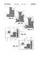
- FIG. 1Aillustrates a clear field pattern feature
- FIG. 1Billustrates the feature shown in FIG. 1A with positive and negative serif correction features.
- FIG. 1Cillustrates the original feature shown in FIG. 1B with interior and exterior edge bar features.
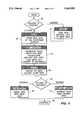
- FIG. 2is a flowchart showing the steps for synthesizing correction features for an entire mask pattern according to one embodiment of the present invention.
- FIG. 3Aillustrates a clear field mask pattern divided into six non-overlapping tiles.
- FIG. 3Billustrates an oversized tile with respect to the non-overlapping tile.
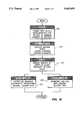
- FIG. 4illustrates a flowchart showing the steps of synthesizing scattering bars according to one embodiment of the present invention.
- FIG. 5Ashows a dark field mask pattern having interior and exterior scattering bar features.
- FIG. 5Bshows a clear field mask pattern having interior and exterior scattering bar features.
- FIGS. 6A-6Eillustrate a feature after performing geometric operations to generate interior scattering bars.
- FIGS. 7A-7Dillustrate a feature after performing geometric operations to generate exterior scattering bars.
- FIGS. 8A-8Dillustrate a method for synthesizing exterior bar features according to one embodiment of the present invention.
- FIGS. 9A-9Dillustrate a method for synthesizing interior bar features according to one embodiment of the present invention.
- FIG. 10illustrates a flowchart showing the steps of serif synthesis according to one embodiment of the present invention.
- a method for generating correction features for an entire mask patternis described.
- numerous specific detailsare set forth, such as data formatting types, proximity correction feature types, mask design rules, and geometry engine type in order to provide a thorough understanding of the present invention. It will be obvious, however, to one skilled in the art that these specific details need not be employed to practice the present invention. In other instances, well-known lithographic techniques, geometric pattern manipulation techniques, and e-beam mask making technologies have not been described in detail in order to avoid unnecessarily obscuring the present invention.
- Photolithographic masksconsist of geometric patterns corresponding to the circuit components to be integrated into a silicon wafer. Each mask is used to transfer its corresponding pattern to a photosensitive layer of material (i.e. photoresist) deposited on a silicon substrate.
- a photosensitive layer of materiali.e. photoresist
- the minimum dimension of its corresponding mask patternapproaches the resolution limit of the optical exposure tool (i.e. the optical tool's minimum transferable dimension) being utilized to transfer the pattern.
- the optical exposure tooli.e. the optical tool's minimum transferable dimension
- many pattern transference problemsbegin to occur. Often times these problems are attributed to phenomena referred to as "proximity effects”.
- Proximity effectsoccur when very closely spaced pattern features are lithographically transferred to a resist layer on a wafer.
- the light waves of the closely spaced featuresinteract and, as a result, distort the final transferred pattern features.
- Another problem that occurs when feature sizes and spacing approach the resolution limit of the lithographic toolis that corners (concave and convex) tend to overexpose or underexpose due to a concentration or scarcity of energy at each of the corners.
- Other types of problemssuch as over- or under-exposure of small features when large and small features are transferred from the same mask pattern, also occur.
- One technique utilized in the photolithography industry to overcome these types of proximity effectsis to add additional features to the original mask pattern. These additional features are typically sub-lithographic (i.e. have dimensions less than the resolution of the exposure tool) and thus do not transfer to the resist layer. Instead, they interact with the original pattern so as to improve the final transferred pattern and compensate for proximity effects.
- U.S. Pat. No. 5,256,505, U.S. Pat. No. 5,242,770, and pending U.S. patent application Ser. No. 08/194,097 assigned to the assignee of the present inventiondescribe three different types of proximity correction techniques--each adding sub-lithographic proximity correction features to original mask patterns to compensate for proximity effects.
- Another proximity correction techniquethat is commonly used in the industry adds sub-lithographic rectilinear shaped features (referred to as serifs) to original feature corners in order to sharpen corner transference.
- FIG. 1Aillustrates a mask pattern feature 10 and FIGS. 1B and 1C illustrate feature 10 after adding some typical optical correction features to it.
- FIG. 1Billustrates original feature 10 having positive serifs 11 and negative serifs 12 added to it and
- FIG. 1Cillustrates feature 10 having positive and negative serifs (11 and 12) and exterior edge bars 13 and interior edge bars 14 added to it.
- Design rules determining the width and distance of the edge bars and size and placement of serifsare dependent on many factors relating to the lithographic process utilized.
- Non-hierarchical datamay be represented in a number of ways.
- Two representations of interestare edge-based and vertex-based.
- An edge representation of a particular patternconsists of a list of edges, where each edge is described in terms of the spatial coordinates of its two end points.
- a vertex representation of the patternconsists of a list of vertices where each vertex is described in terms of its spatial coordinate, type of vertex (i.e. convex or concave), and direction.
- a vertex representation of the original pattern datais more useful than an edge representation since a vertex representation typically gives information about the type of vertex (convex or concave) and its location.
- an edge representationis more useful when generating edge bars since it describes the length and location of the edge. Processing the data for both a non-hierarchical vertex representation and a non-hierarchical edge representation to determine correction features for an entire mask pattern is simply not within the repertoire of currently-available commercial mask data processing software.
- the present inventionis a unique method for generating more than one type of correction feature for an entire mask pattern while avoiding the memory and processing time limitations that have, heretofore, prevented the development of a commercial solution to this problem.
- the general concept behind the present inventionis to divide the mask pattern data into a number of geometric tiles--each tile containing pattern data corresponding to a section of the original mask pattern. Each individual tile is then processed through a series of correction feature generation phases to generate all of the correction features for that particular tile. The combined original and correction feature data for the tile is then condensed and stored to a secondary memory to free up primary memory for correction feature computation for the next tile of data. New tiles of data are processed through the correction generation phases until all tiles have been processed.
- the tile datais reformatted into a representation that provides the type of information to generate the particular correction feature for the phase.
- the original tile of pattern datais reformatted into vertex representation when computing serifs.
- edge barsthe original tile of pattern data is converted to edge representation. Since the amount of data for each tile is small, the reformatting does not result in large processing delay times.
- the geometry engineprovides a means of performing various operations on geometric pattern data such as pattern sizing (grow/shrink operations), geometric Boolean operations such as AND, OR, XOR, or AND-NOT, and representation conversion.
- FIG. 2illustrates a flowchart showing the steps of one embodiment of the method of the present invention.
- Flatten and Tile block 20involves the steps of taking the hierarchical data for the entire mask pattern, expanding it into non-hierarchical form (i.e. flattening the data), and then dividing the flattened data into many geometric sections (i.e. tiles) within the mask pattern.
- the flattened pattern datais represented in terms of one or more polygons--where each polygon is defined as a closed loop of vertices. It should be apparent that other flattened data formats may also be used. However, whatever the data format, each feature needs to be enumerated at this point.
- FIG. 3A and 3Billustrate the manner in which a data pattern 30 is divided into many tiles.
- clear field data pattern 30consists of features 32-34 and is sectioned into six defined non-overlapping tiles 31.
- FIG. 3Billustrates the manner in which the data corresponding to a pattern 30 is actually divided in accordance to the method of the present invention.
- the data for pattern 30is divided into six overlapping tiles as illustrated by tile 35 in FIG. 3B, (only one overlapping tile 35 is shown in FIG. 3B for clarity).
- Tilesare overlapped to account for cases in which feature edges reside close to the boundary defined by the non-overlapping tiles 31 (e.g. feature 32, FIG. 3B) or cross over the boundary defined by the non-overlapping tiles 31 (e.g. features 33 and 34, FIG. 3B).
- each tileis processed through two correction feature generation phases (blocks 21 and 22, FIG. 2).
- Block 21synthesizes scattering bars and anti-scattering bars (as taught by U.S. patent application Ser. No. 08/194,097) for all edges residing within the particular tile being processed.
- Block 22performs the serif synthesis for all corners residing within the tile being processed. It should be understood that although blocks 21 and 22 are each associated with a particular type of correction feature, any other type of correction feature may be generated within these blocks.
- the number of correction feature generation phasesis not limited to only two phases, instead, more phases may be added. Further, the order of generation phases can be different than what is shown in FIG. 2.
- Scattering bar generation phase 21utilizes the original data corresponding to a given tile to generate 1) a data set of computed exterior bars for the tile and 2) a modified data set corresponding to the result of a geometrical subtraction between the data corresponding to the tile's computed interior bars and the original tile data.
- serif generation phase 22utilizes the original data corresponding to the tile to generate: 1) a data file of computed positive serifs and 2) a modified data file corresponding to the result of a geometric subtraction between the modified tile data from the previous block (i.e. block 21) and the data corresponding to the tile's computed negative serifs.
- three data setshave been generated, 1) a set containing data representing a modified pattern having both negative serifs and interior bars, 2) a set containing data representing the positive serifs for the tile and 3) a set containing data representing the exterior bars for the tile.
- These three setsare concatenated into a single set representing the tile data having all of the correction features applied to it. This single data set is then clipped to the exact size of the original non-overlapping tile, eliminating all redundant and erroneous data in the overlap region.
- This data setis then processed through a compaction phase 23.
- the particular geometry engine employed in the preferred embodiment of the present inventionperforms compaction phase 23 by initially identifying similar features and feature locations and then, with this information, identifying repeating geometric patterns within the file data.
- the geometry enginerepresents the repetitive patterns as two-dimensional arrays of repeating cells by describing one of the repetitive features and then applying a property to that feature which indicates that it is replicated in a certain number of rows and columns having a defined horizontal and vertical spacing.
- the advantage of applying compaction at this point in the processingis that repetitive correction feature patterns may also be compacted along with the original pattern data. Consequently, compaction phase 23 greatly reduces the amount of data put in the final data pattern file.
- the final compacted data set for the tileis then stored in a pattern file.
- This pattern fileholds all of the data corresponding to all of the tiles once they have been processed through blocks 21-23.
- the pattern fileis typically stored in secondary memory (i.e. disk file) in order to make room in primary memory for computing correction features for the next tile.
- the data for the next tileis retrieved and processed through blocks 21-24.
- the final pattern filecontains data representing the entire data pattern having correction features applied to every feature. This final pattern file data may then be processed through other steps prior to using it to create the lithographic mask if necessary.
- FIG. 4is a flowchart illustrating one embodiment of the method for synthesizing scattering bars and anti-scattering bars as described in FIG. 2 (i.e. block 21) according to the present invention.
- the processing stepsapply to dark field mask pattern data.
- a dark field mask patternis a pattern in which the feature area is clear and the area surrounding the feature is dark.
- Scattering barsare opaque features on the final mask, but may be computed as either "interior” or “exterior” with respect to the original feature data, depending on whether the final mask is dark or clear field.
- Anti-scattering barsare by definition clear but may also be either interior or exterior to the original feature depending on the type of mask field used.
- FIG. 5Aillustrates a dark field mask pattern 50 having a feature 51 with interior scattering bars 52 and exterior anti-scattering bars 53.
- FIG. 5Billustrates a clear field mask pattern 59 having a feature 55 with exterior scattering bars 57 and interior anti-scattering bars 56.
- an interior baris one that resides within the original feature having the opposite opaqueness as the original feature and an exterior bar is one that resides outside of the original feature having the same opaqueness as the original feature.
- Block 40determines whether interior or exterior bars are to be computed. If interior bars are computed; the tile pattern data is initially inverted as indicated by block 41, (i.e. the geometry engine makes the clear areas dark and the dark areas clear). If exterior bars are being computed, then the tile data is directly passed to block 42 without inverting the data first.
- a grow operation(block 42) is performed.
- a growis performed on the inverted data.
- Scattering bar synthesis(block 43) is performed by growing each edge (a one-dimensional feature) into a scattering bar (a two-dimensional feature).
- FIGS. 6A-Eillustrates the geometric operations performed to generate interior scattering bars for an original feature 61 in a clear field mask pattern 60.
- FIG. 6Billustrates mask pattern 60 after it has been inverted such that feature 61 is clear and the surrounding area is dark.
- FIG. 6Cillustrates pattern 60 after a grow operation wherein clear feature 64 is generated, (note: in a clear field grow operation, the clear areas become smaller, while the dark areas are expanded).
- FIG. 6Dillustrates the edge representation of feature 64 consisting of edges 65-68.
- FIG. 6Eillustrates expanding each of edges 65-68 into a two-dimensional interior scattering bar.
- FIGS. 7A-Dillustrate the geometric operations performed to create exterior scattering bars for an original feature 71 in a clear field mask pattern 70.
- FIG. 7Billustrates mask pattern 70 after a grow operation wherein oversized feature 73 is generated.
- FIG. 7Cillustrates the edge representation of feature 73 including edges 74-77 and
- FIG. 7Dshows the exterior edge bars generated by expanding each of edges 74-77 into a two-dimensional bar.
- the method for synthesizing interior and exterior barsis not restricted to the method as described in blocks 41-43 and FIGS. 6 and 7.
- feature datacan be shrunk (the opposite of a grow operation) to determine edges 65-68 in FIG. 6D followed by expanding the edges into bars.
- external barsmay be synthesized by first inverting and then shrinking to determine edges 74-77 in FIG. 7C followed by expanding the edges into bars.
- the general concept behind the technique of the present invention for synthesizing either internal or external correction barsis the displacement of the original feature edges (whether by inverting first and then shrinking or growing or just by shrinking or growing) to the location at which the bar is to be synthesized and then expanding the edge into a bar.
- One other method for synthesizing correction barsis achieved by performing a first grow or shrink operation on feature data (depending on whether interior or exterior bars are being synthesized) to generate first grown/shrunk data.
- the first grow/shrink operationdefines a first set of interior edges of the correction bar being synthesized.
- a second grow/shrink operationis performed on the first grow/shrink data to generate second grown/shrunk data.
- the second grow/shrink operationis performed to define a second set of exterior edges.
- the first grow/shrink datais geometrically subtracted from the second grow/shrink data to generate a ring of correction bars.
- FIGS. 8A-8D and 9A-9Dshow a method for synthesizing exterior bar data for a feature 81
- FIGS. 9A-9Dshow a method for synthesizing interior bar data for feature 91.
- FIG. 8Aillustrates a feature 81 and FIG. 8B illustrates a feature 82 after a grow operation is performed on feature 81.
- FIG. 8Cshows a feature 83 which results from a subsequent grow operation on either of features 81 or 82.
- FIG. 8Dshows the synthesized correction feature after feature 82 has been geometrically subtracted from feature 83. This external bar feature would then be geometrically added to feature 81.
- FIG. 9Aillustrates a feature 91 and FIG. 9B illustrates a feature 92 after a shrink operation is performed on feature 91.
- FIG. 9Cshows a feature 93 which results from a subsequent shrink operation on either of features 91 or 92.
- FIG. 9Dshows the synthesized correction feature after feature 93 has been geometrically subtracted from feature 92. This internal bar feature would then be geometrically subtracted from feature 91.
- each bar in the listis checked to see if it is an illegal bar.
- Illegal barsoccur when; 1) two primary features are spaced such that no bar should be synthesized, 2) two primary features are close enough to generate two bars that are spaced too close together, or 3) two primary features generate two overlapping bars resulting in a single fat bar. Once identified, all illegal bars are eliminated. In addition, any other bar fragments generated in the bar synthesis are eliminated. In the case where bars are spaced too close (illegal case 2) or when a fat bar is generated (illegal case 3), a single bar is generated between the two original features that is located equally between the two features, as designated by the design rules.
- FIG. 10illustrates the steps for synthesizing serifs according to one method of the present invention.
- Block 100includes the steps of reformatting the data representation of the original tile data into a vertex representation. In vertex representation, each vertex is enumerated in terms of its spatial coordinates, its type (convex or concave), and its direction. Block 100 also includes a merge step that entails eliminating any redundant vertices in the original data, such as those arising from "construction lines" where two rectangular features abut one another.
- serifsare synthesized from this list of vertices (block 101 ) utilizing software routines provided by the geometry engine. The size and placement of the serifs are dependent on the lithographic design rules. For each convex/concave vertex, a positive/negative serif (see FIG. 1B) is computed. After serif generation, the list of serifs is examined to filter out any serifs that are too close to one another (block 102). The positive serifs are concatenated with (block 103) and the negative serifs are geometrically subtracted from the modified tile data set generated in the previous scattering bar phase (block 104).
Landscapes
- Physics & Mathematics (AREA)
- General Physics & Mathematics (AREA)
- Preparing Plates And Mask In Photomechanical Process (AREA)
Abstract
Description
Claims (15)
Priority Applications (7)
| Application Number | Priority Date | Filing Date | Title |
|---|---|---|---|
| US08/433,730US5663893A (en) | 1995-05-03 | 1995-05-03 | Method for generating proximity correction features for a lithographic mask pattern |
| JP53332496AJP3922308B2 (en) | 1995-05-03 | 1996-04-17 | Proximity effect correction feature generation method for lithographic mask patterns |
| PCT/US1996/005224WO1996035145A1 (en) | 1995-05-03 | 1996-04-17 | Method for generating proximity correction features for a lithographic mask pattern |
| KR1019970707783AKR100401381B1 (en) | 1995-05-03 | 1996-04-17 | How to form proximity correction features for lithographic mask patterns |
| AU53915/96AAU5391596A (en) | 1995-05-03 | 1996-04-17 | Method for generating proximity correction features for a li thographic mask pattern |
| TW085104839ATW311234B (en) | 1995-05-03 | 1996-04-23 | |
| JP2006230628AJP3996620B2 (en) | 1995-05-03 | 2006-08-28 | Proximity effect correction feature generation method for lithographic mask patterns |
Applications Claiming Priority (1)
| Application Number | Priority Date | Filing Date | Title |
|---|---|---|---|
| US08/433,730US5663893A (en) | 1995-05-03 | 1995-05-03 | Method for generating proximity correction features for a lithographic mask pattern |
Publications (1)
| Publication Number | Publication Date |
|---|---|
| US5663893Atrue US5663893A (en) | 1997-09-02 |
Family
ID=23721321
Family Applications (1)
| Application Number | Title | Priority Date | Filing Date |
|---|---|---|---|
| US08/433,730Expired - LifetimeUS5663893A (en) | 1995-05-03 | 1995-05-03 | Method for generating proximity correction features for a lithographic mask pattern |
Country Status (6)
| Country | Link |
|---|---|
| US (1) | US5663893A (en) |
| JP (2) | JP3922308B2 (en) |
| KR (1) | KR100401381B1 (en) |
| AU (1) | AU5391596A (en) |
| TW (1) | TW311234B (en) |
| WO (1) | WO1996035145A1 (en) |
Cited By (123)
| Publication number | Priority date | Publication date | Assignee | Title |
|---|---|---|---|---|
| US5740068A (en)* | 1996-05-30 | 1998-04-14 | International Business Machines Corporation | Fidelity enhancement of lithographic and reactive-ion-etched images by optical proximity correction |
| US5844809A (en)* | 1995-07-28 | 1998-12-01 | Kabushiki Kaisha Toshiba | Method and apparatus for generating two-dimensional circuit pattern |
| US5862058A (en)* | 1996-05-16 | 1999-01-19 | International Business Machines Corporation | Optical proximity correction method and system |
| US5877964A (en)* | 1997-01-10 | 1999-03-02 | International Business Machines Corporation | Semiconductor device compensation system and method |
| US5887155A (en)* | 1996-07-25 | 1999-03-23 | Microunity Systems Engineering, Inc. | Vertex based geometry engine system for use in integrated circuit design |
| US5885734A (en)* | 1996-08-15 | 1999-03-23 | Micron Technology, Inc. | Process for modifying a hierarchical mask layout |
| WO1999027420A1 (en)* | 1997-11-24 | 1999-06-03 | Asml Masktools Netherlands B.V. | Method of fine feature edge tuning with optically-halftoned mask |
| US5912983A (en)* | 1997-01-24 | 1999-06-15 | Oki Electric Industry Co., Ltd | Overlay accuracy measuring method |
| US5920487A (en)* | 1997-03-03 | 1999-07-06 | Motorola Inc. | Two dimensional lithographic proximity correction using DRC shape functions |
| US6077310A (en)* | 1995-12-22 | 2000-06-20 | Kabushiki Kaisha Toshiba | Optical proximity correction system |
| US6120952A (en)* | 1998-10-01 | 2000-09-19 | Micron Technology, Inc. | Methods of reducing proximity effects in lithographic processes |
| US6127071A (en)* | 1999-06-22 | 2000-10-03 | International Business Machines Corporation | Serif mask design for correcting severe corner rounding and line end shortening in lithography |
| US6175953B1 (en)* | 1998-03-03 | 2001-01-16 | Lsi Logic Corporation | Method and apparatus for general systematic application of proximity correction |
| US6183920B1 (en) | 1998-07-08 | 2001-02-06 | Matsushita Electric Industrial Co., Ltd. | Semiconductor device geometrical pattern correction process and geometrical pattern extraction process |
| US6214494B1 (en) | 1998-10-07 | 2001-04-10 | International Business Machines Corporation | Serif mask design methodology based on enhancing high spatial frequency contribution for improved printability |
| US6226781B1 (en)* | 1998-08-12 | 2001-05-01 | Advanced Micro Devices, Inc. | Modifying a design layer of an integrated circuit using overlying and underlying design layers |
| US6258493B1 (en) | 1996-09-18 | 2001-07-10 | Numerical Technologies, Inc. | Phase shifting circuit manufacture method and apparatus |
| US6269472B1 (en)* | 1996-02-27 | 2001-07-31 | Lsi Logic Corporation | Optical proximity correction method and apparatus |
| US6282696B1 (en)* | 1997-08-15 | 2001-08-28 | Lsi Logic Corporation | Performing optical proximity correction with the aid of design rule checkers |
| US6312854B1 (en) | 1998-03-17 | 2001-11-06 | Asml Masktools Netherlands B.V. | Method of patterning sub-0.25 lambda line features with high transmission, “attenuated” phase shift masks |
| EP1164432A1 (en)* | 2000-06-13 | 2001-12-19 | ASML Masktools Netherlands B.V. | Optical proximity correction method utilizing serifs having variable dimensions |
| WO2001097096A1 (en)* | 2000-06-13 | 2001-12-20 | Mentor Graphics Corporation | Integrated verification and manufacturability tool |
| WO2001097048A1 (en)* | 2000-06-13 | 2001-12-20 | Mentor Graphics Corporation | Integrated verification and manufacturability tool |
| US6335130B1 (en) | 2000-05-01 | 2002-01-01 | Asml Masktools Netherlands B.V. | System and method of providing optical proximity correction for features using phase-shifted halftone transparent/semi-transparent features |
| US6343370B1 (en)* | 1997-12-05 | 2002-01-29 | Mitsubishi Denki Kabusiki Kaisha | Apparatus and process for pattern distortion detection for semiconductor process and semiconductor device manufactured by use of the apparatus or process |
| US6360134B1 (en)* | 1998-07-20 | 2002-03-19 | Photronics, Inc. | Method for creating and improved image on a photomask by negatively and positively overscanning the boundaries of an image pattern at inside corner locations |
| US6370679B1 (en) | 1997-09-17 | 2002-04-09 | Numerical Technologies, Inc. | Data hierarchy layout correction and verification method and apparatus |
| US6421820B1 (en) | 1999-12-13 | 2002-07-16 | Infineon Technologies Ag | Semiconductor device fabrication using a photomask with assist features |
| US6430733B1 (en) | 1999-04-22 | 2002-08-06 | International Business Machines Corporation | Contextual based groundrule compensation method of mask data set generation |
| US6453457B1 (en) | 2000-09-29 | 2002-09-17 | Numerical Technologies, Inc. | Selection of evaluation point locations based on proximity effects model amplitudes for correcting proximity effects in a fabrication layout |
| US6453452B1 (en) | 1997-12-12 | 2002-09-17 | Numerical Technologies, Inc. | Method and apparatus for data hierarchy maintenance in a system for mask description |
| US6470489B1 (en) | 1997-09-17 | 2002-10-22 | Numerical Technologies, Inc. | Design rule checking system and method |
| US20020166108A1 (en)* | 1999-10-08 | 2002-11-07 | Dupont Photomasks, Inc., A Delaware Corporation | System and method for correcting connectivity errors in a mask layout file |
| US20020170031A1 (en)* | 2001-02-28 | 2002-11-14 | Nec Corporation | Method for manufacturing a pair of complementary masks |
| US20020186356A1 (en)* | 2001-02-27 | 2002-12-12 | Smith Bruce W. | Optical proximity correction method utilizing gray bars as sub-resolution assist features |
| US6499003B2 (en)* | 1998-03-03 | 2002-12-24 | Lsi Logic Corporation | Method and apparatus for application of proximity correction with unitary segmentation |
| US20020199157A1 (en)* | 1999-04-30 | 2002-12-26 | Cobb Nicolas Bailey | Mixed-mode optical proximity correction |
| US6523162B1 (en) | 2000-08-02 | 2003-02-18 | Numerical Technologies, Inc. | General purpose shape-based layout processing scheme for IC layout modifications |
| US6539521B1 (en) | 2000-09-29 | 2003-03-25 | Numerical Technologies, Inc. | Dissection of corners in a fabrication layout for correcting proximity effects |
| US6546532B1 (en) | 2000-06-20 | 2003-04-08 | Unisys Corporation | Method and apparatus for traversing and placing cells using a placement tool |
| US6548224B1 (en) | 2000-03-07 | 2003-04-15 | Kulicke & Soffa Holdings, Inc. | Wiring substrate features having controlled sidewall profiles |
| US20030097647A1 (en)* | 2000-02-28 | 2003-05-22 | Numerical Technologies, Inc. | Method and apparatus for mixed-mode optical proximity correction |
| US6571383B1 (en) | 2000-04-28 | 2003-05-27 | Infineon Technologies, Ag | Semiconductor device fabrication using a photomask designed using modeling and empirical testing |
| US6578188B1 (en) | 1997-09-17 | 2003-06-10 | Numerical Technologies, Inc. | Method and apparatus for a network-based mask defect printability analysis system |
| US6596466B1 (en)* | 2000-01-25 | 2003-07-22 | Cypress Semiconductor Corporation | Contact structure and method of forming a contact structure |
| US6601231B2 (en) | 2001-07-10 | 2003-07-29 | Lacour Patrick Joseph | Space classification for resolution enhancement techniques |
| US20030145353A1 (en)* | 1997-05-07 | 2003-07-31 | Lightner Jonathan E. | Starch biosynthetic enzymes |
| US20030163791A1 (en)* | 2001-12-31 | 2003-08-28 | Numerical Technologies, Inc. | Shape-based geometry engine to perform smoothing and other layout beautification operations |
| US6615393B1 (en)* | 2001-06-25 | 2003-09-02 | Cypress Semiconductor Corporation | Method and apparatus for performing electrical distance check |
| US20030174341A1 (en)* | 2002-02-12 | 2003-09-18 | Hill Henry A. | Characterization and compensation of non-cyclic errors in interferometry systems |
| US6625801B1 (en) | 2000-09-29 | 2003-09-23 | Numerical Technologies, Inc. | Dissection of printed edges from a fabrication layout for correcting proximity effects |
| US6623895B2 (en) | 2000-05-01 | 2003-09-23 | Asml Masktools Netherlands B.V. | Hybrid phase-shift mask |
| US6631307B1 (en)* | 1998-03-19 | 2003-10-07 | Taiwan Semiconductor Manufacturing Company | Use of logical operations in place of OPC software |
| US20030211400A1 (en)* | 2000-02-14 | 2003-11-13 | Smith Bruce W | Method of improving photomask geometry |
| US6653026B2 (en) | 2000-12-20 | 2003-11-25 | Numerical Technologies, Inc. | Structure and method of correcting proximity effects in a tri-tone attenuated phase-shifting mask |
| US6660439B1 (en) | 2002-04-08 | 2003-12-09 | Taiwan Semiconductor Manufacturing Company | Method to reduce data size and data preparation time for optical proximity correction of photo masks |
| US6665856B1 (en)* | 2000-12-01 | 2003-12-16 | Numerical Technologies, Inc. | Displacing edge segments on a fabrication layout based on proximity effects model amplitudes for correcting proximity effects |
| US20030233630A1 (en)* | 2001-12-14 | 2003-12-18 | Torbjorn Sandstrom | Methods and systems for process control of corner feature embellishment |
| US6670082B2 (en) | 2001-10-09 | 2003-12-30 | Numerical Technologies, Inc. | System and method for correcting 3D effects in an alternating phase-shifting mask |
| US6670646B2 (en) | 2002-02-11 | 2003-12-30 | Infineon Technologies Ag | Mask and method for patterning a semiconductor wafer |
| US20040015808A1 (en)* | 1997-09-17 | 2004-01-22 | Numerical Technologies, Inc. | System and method for providing defect printability analysis of photolithographic masks with job-based automation |
| US6684382B2 (en) | 2001-08-31 | 2004-01-27 | Numerical Technologies, Inc. | Microloading effect correction |
| US6684376B1 (en)* | 1997-01-27 | 2004-01-27 | Unisys Corporation | Method and apparatus for selecting components within a circuit design database |
| US20040031005A1 (en)* | 2002-03-08 | 2004-02-12 | Umc Japan | Electronic cad system and layout data producing method therefor |
| US6698008B2 (en) | 2001-10-30 | 2004-02-24 | International Business Machines Corporation | Row-based placement scoring and legalization measure for books with phase shift mask dependencies |
| US6703167B2 (en) | 2001-04-18 | 2004-03-09 | Lacour Patrick Joseph | Prioritizing the application of resolution enhancement techniques |
| US20040063000A1 (en)* | 2002-09-27 | 2004-04-01 | Mentor Graphics Corporation | Chromeless phase mask layout generation |
| US20040085546A1 (en)* | 2002-09-09 | 2004-05-06 | Hill Henry A. | Measurement and compensation of errors in interferometers |
| US20040101790A1 (en)* | 2002-11-27 | 2004-05-27 | John Cauchi | Photolithography method including a double exposure/double bake |
| US6747744B2 (en) | 2000-11-20 | 2004-06-08 | Zygo Corporation | Interferometric servo control system for stage metrology |
| US6753116B2 (en) | 2002-01-25 | 2004-06-22 | Mosel Vitelic, Inc. | Multiple photolithographic exposures with different non-clear patterns |
| US6757645B2 (en) | 1997-09-17 | 2004-06-29 | Numerical Technologies, Inc. | Visual inspection and verification system |
| US20040128638A1 (en)* | 2000-06-20 | 2004-07-01 | Kerzman Joseph Peter | Method and apparatus for selecting and aligning cells using a placement tool |
| US20040135980A1 (en)* | 2002-12-12 | 2004-07-15 | Hill Henry A. | In-process correction of stage mirror deformations during a photolithography exposure cycle |
| US6777168B2 (en) | 2001-12-14 | 2004-08-17 | Mosel Vitelic, Inc. | Multiple photolithographic exposures with different clear patterns |
| US6792590B1 (en) | 2000-09-29 | 2004-09-14 | Numerical Technologies, Inc. | Dissection of edges with projection points in a fabrication layout for correcting proximity effects |
| US20050022150A1 (en)* | 2003-07-23 | 2005-01-27 | Shu-Hui Liu | Optical proximity correction method |
| US20050018206A1 (en)* | 2003-06-19 | 2005-01-27 | Hill Henry A. | Compensation for geometric effects of beam misalignments in plane mirror interferometer metrology systems |
| US6849364B2 (en) | 2001-08-23 | 2005-02-01 | Infineon Technologies Ag | Mask for fabricating semiconductor components |
| US20050028129A1 (en)* | 2003-06-30 | 2005-02-03 | Hsu Duan-Fu Stephen | Method, program product and apparatus of simultaneous optimization for NA-Sigma exposure settings and scattering bars OPC using a device layout |
| US20050076322A1 (en)* | 2003-10-07 | 2005-04-07 | Jun Ye | System and method for lithography simulation |
| US20050074677A1 (en)* | 2003-06-30 | 2005-04-07 | Thomas Laidig | Scattering bar OPC application method for sub-half wavelength lithography patterning |
| US6881523B2 (en) | 2001-03-14 | 2005-04-19 | Asml Masktools B.V. | Optical proximity correction method utilizing ruled ladder bars as sub-resolution assist features |
| US20050091013A1 (en)* | 2003-10-27 | 2005-04-28 | International Business Machines Corporation | Incorporation of a phase map into fast model-based optical proximity correction simulation kernels to account for near and mid-range flare |
| US20050096888A1 (en)* | 2001-05-11 | 2005-05-05 | Ismail Yehea I. | Efficient model order reduction via multi-point moment matching |
| US6893779B2 (en) | 2001-03-20 | 2005-05-17 | Samsung Electronics, Co., Ltd. | Phase shifting mask for manufacturing semiconductor device and method of fabricating the same |
| US20050129328A1 (en)* | 2003-12-15 | 2005-06-16 | Xerox Corporation | Corner sharpening of text and line art in a super resolution anti-aliasing image path |
| US20050134862A1 (en)* | 2003-11-04 | 2005-06-23 | Zygo Corporatin | Characterization and compensation of errors in multi-axis interferometry systems |
| US20050142449A1 (en)* | 2003-09-05 | 2005-06-30 | Xuelong Shi | Method and apparatus for performing model based placement of phase-balanced scattering bars for sub-wavelength optical lithography |
| US20050146727A1 (en)* | 2004-01-06 | 2005-07-07 | Hill Henry A. | Multi-axis interferometers and methods and systems using multi-axis interferometers |
| US20050151951A1 (en)* | 2004-01-05 | 2005-07-14 | Zygo Corporation | Stage alignment in lithography tools |
| US20050157309A1 (en)* | 2002-09-09 | 2005-07-21 | Hill Henry A. | Measurement and compensation of errors in interferometers |
| US20050162664A1 (en)* | 2002-07-29 | 2005-07-28 | Zygo Corporation | Compensation for errors in off-axis interferometric measurements |
| US20050202326A1 (en)* | 2004-03-09 | 2005-09-15 | International Business Machines Corporation | Optimized placement of sub-resolution assist features within two-dimensional environments |
| US20050208396A1 (en)* | 2002-10-18 | 2005-09-22 | Mentor Graphics Corporation | Short edge smoothing for enhanced scatter bar placement |
| US20050229130A1 (en)* | 2004-04-07 | 2005-10-13 | Aprio Technologies, Inc. | Method and apparatus for selective, incremental, reconfigurable and reusable semiconductor manufacturing resolution-enhancements |
| US20050237536A1 (en)* | 2004-04-22 | 2005-10-27 | Hill Henry A | Interferometry systems and methods of using interferometry systems |
| US20050280800A1 (en)* | 2004-04-09 | 2005-12-22 | Thomas Laiding | Optical proximity correction using chamfers and rounding at corners |
| US20060005154A1 (en)* | 2000-06-13 | 2006-01-05 | Mentor Graphics Corporation | Integrated OPC verification tool |
| US20060061771A1 (en)* | 2003-06-19 | 2006-03-23 | Hill Henry A | Compensation for effects of beam misalignments in interferometer metrology systems |
| US20060072119A1 (en)* | 2004-10-06 | 2006-04-06 | Hill Henry A | Error correction in interferometry systems |
| US20060075380A1 (en)* | 2004-09-29 | 2006-04-06 | Dan Beale | Calculating etch proximity-correction using object-precision techniques |
| US20060187464A1 (en)* | 2004-04-22 | 2006-08-24 | Gary Womack | Interferometry systems and methods of using interferometry systems |
| US20060215173A1 (en)* | 2005-03-18 | 2006-09-28 | Hill Henry A | Multi-axis interferometer with procedure and data processing for mirror mapping |
| US20060236296A1 (en)* | 2005-03-17 | 2006-10-19 | Melvin Lawrence S Iii | Method and apparatus for identifying assist feature placement problems |
| US20060242619A1 (en)* | 1997-09-17 | 2006-10-26 | Synopsys, Inc. | System And Method For Providing Defect Printability Analysis Of Photolithographic Masks With Job-Based Automation |
| US20080077907A1 (en)* | 2006-09-21 | 2008-03-27 | Kulkami Anand P | Neural network-based system and methods for performing optical proximity correction |
| US20080099676A1 (en)* | 2006-10-31 | 2008-05-01 | Hitachi High-Technologies Corporation | Scanning electron microscope and a method for pattern composite inspection using the same |
| US20080216045A1 (en)* | 2006-11-28 | 2008-09-04 | Sachiko Kobayashi | Mask data processing method for optimizing hierarchical structure |
| US20080216047A1 (en)* | 2004-04-07 | 2008-09-04 | Aprio Technololgies, Inc. | Intermediate Layout for Resolution Enhancement in Semiconductor Fabrication |
| US7558419B1 (en) | 2003-08-14 | 2009-07-07 | Brion Technologies, Inc. | System and method for detecting integrated circuit pattern defects |
| US20110099526A1 (en)* | 2009-10-28 | 2011-04-28 | Asml Netherlands B.V. | Pattern Selection for Full-Chip Source and Mask Optimization |
| WO2013178459A1 (en) | 2012-05-31 | 2013-12-05 | Asml Netherlands B.V. | Gradient-based pattern and evaluation point selection |
| US8850366B2 (en)* | 2012-08-01 | 2014-09-30 | Taiwan Semiconductor Manufacturing Company, Ltd. | Method for making a mask by forming a phase bar in an integrated circuit design layout |
| US20140331191A1 (en)* | 2013-05-06 | 2014-11-06 | United Microelectronics Corp. | Method of correcting assist feature |
| US8893060B2 (en) | 2010-11-10 | 2014-11-18 | Asml Netherlands B.V. | Optimization of source, mask and projection optics |
| US9524364B1 (en)* | 2014-09-23 | 2016-12-20 | Cadence Design Systems, Inc. | Method and system for creating improved routing polygon abstracts |
| US9576098B2 (en)* | 2006-07-21 | 2017-02-21 | Synopsys, Inc. | Lithography aware leakage analysis |
| US9588438B2 (en) | 2010-11-10 | 2017-03-07 | Asml Netherlands B.V. | Optimization flows of source, mask and projection optics |
| CN107479331A (en)* | 2017-07-31 | 2017-12-15 | 上海华力微电子有限公司 | A kind of OPC modification methods of figure corner |
| CN111316174A (en)* | 2017-11-30 | 2020-06-19 | 国际商业机器公司 | Optical mask verification |
| US11372324B2 (en) | 2019-02-11 | 2022-06-28 | United Microelectronics Corporation | Method for correcting mask pattern and mask pattern thereof |
| KR20220154599A (en)* | 2021-05-13 | 2022-11-22 | 타이완 세미콘덕터 매뉴팩쳐링 컴퍼니 리미티드 | Geometric mask rule check with favorable and unfavorable zones |
Families Citing this family (6)
| Publication number | Priority date | Publication date | Assignee | Title |
|---|---|---|---|---|
| JP4460794B2 (en)* | 2001-04-23 | 2010-05-12 | 株式会社東芝 | Exposure mask pattern correction method, pattern formation method, and program |
| JP2003045780A (en)* | 2001-07-30 | 2003-02-14 | Nec Corp | Method for preparing mask lithographic data |
| JP4098502B2 (en)* | 2001-07-30 | 2008-06-11 | 株式会社東芝 | Mask manufacturing method and LSI manufacturing method |
| KR100442879B1 (en)* | 2002-07-18 | 2004-08-02 | 삼성전자주식회사 | Method for designing phase grating pattern providing optimum modified illumination to target patterns and method for manufacturing photo mask using therewith |
| EP1719018A1 (en)* | 2004-02-25 | 2006-11-08 | Micronic Laser Systems Ab | Methods for exposing patterns and emulating masks in optical maskless lithography |
| US20240176229A1 (en)* | 2021-03-29 | 2024-05-30 | Citizen Watch Co., Ltd. | Method for manufacturing electroforming mold and photomask |
Citations (10)
| Publication number | Priority date | Publication date | Assignee | Title |
|---|---|---|---|---|
| US4504558A (en)* | 1980-07-10 | 1985-03-12 | International Business Machines Corporation | Method of compensating the proximity effect in electron beam projection systems |
| US4717644A (en)* | 1982-12-20 | 1988-01-05 | International Business Machines Corporation | Hybrid electron beam and optical lithography method |
| US5082762A (en)* | 1988-10-24 | 1992-01-21 | Fujitsu Limited | Charged particle beam exposure method |
| US5241185A (en)* | 1991-01-24 | 1993-08-31 | International Business Machines Corporation | Proximity correction method for e-beam lithography |
| US5242770A (en)* | 1992-01-16 | 1993-09-07 | Microunity Systems Engineering, Inc. | Mask for photolithography |
| US5251140A (en)* | 1991-07-26 | 1993-10-05 | International Business Machines Corporation | E-beam control data compaction system and method |
| US5294800A (en)* | 1992-07-31 | 1994-03-15 | International Business Machines Corporation | E-beam control data compaction system and method |
| US5432714A (en)* | 1993-01-29 | 1995-07-11 | International Business Machines Corporation | System and method for preparing shape data for proximity correction |
| US5447810A (en)* | 1994-02-09 | 1995-09-05 | Microunity Systems Engineering, Inc. | Masks for improved lithographic patterning for off-axis illumination lithography |
| US5475766A (en)* | 1991-09-05 | 1995-12-12 | Kabushiki Kaisha Toshiba | Pattern inspection apparatus with corner rounding of reference pattern data |
Family Cites Families (3)
| Publication number | Priority date | Publication date | Assignee | Title |
|---|---|---|---|---|
| US4895780A (en)* | 1987-05-13 | 1990-01-23 | General Electric Company | Adjustable windage method and mask for correction of proximity effect in submicron photolithography |
| US5208124A (en)* | 1991-03-19 | 1993-05-04 | Hewlett-Packard Company | Method of making a mask for proximity effect correction in projection lithography |
| US5256505A (en)* | 1992-08-21 | 1993-10-26 | Microunity Systems Engineering | Lithographical mask for controlling the dimensions of resist patterns |
- 1995
- 1995-05-03USUS08/433,730patent/US5663893A/ennot_activeExpired - Lifetime
- 1996
- 1996-04-17AUAU53915/96Apatent/AU5391596A/ennot_activeAbandoned
- 1996-04-17JPJP53332496Apatent/JP3922308B2/ennot_activeExpired - Fee Related
- 1996-04-17WOPCT/US1996/005224patent/WO1996035145A1/enactiveIP Right Grant
- 1996-04-17KRKR1019970707783Apatent/KR100401381B1/ennot_activeExpired - Lifetime
- 1996-04-23TWTW085104839Apatent/TW311234B/zhnot_activeIP Right Cessation
- 2006
- 2006-08-28JPJP2006230628Apatent/JP3996620B2/ennot_activeExpired - Lifetime
Patent Citations (10)
| Publication number | Priority date | Publication date | Assignee | Title |
|---|---|---|---|---|
| US4504558A (en)* | 1980-07-10 | 1985-03-12 | International Business Machines Corporation | Method of compensating the proximity effect in electron beam projection systems |
| US4717644A (en)* | 1982-12-20 | 1988-01-05 | International Business Machines Corporation | Hybrid electron beam and optical lithography method |
| US5082762A (en)* | 1988-10-24 | 1992-01-21 | Fujitsu Limited | Charged particle beam exposure method |
| US5241185A (en)* | 1991-01-24 | 1993-08-31 | International Business Machines Corporation | Proximity correction method for e-beam lithography |
| US5251140A (en)* | 1991-07-26 | 1993-10-05 | International Business Machines Corporation | E-beam control data compaction system and method |
| US5475766A (en)* | 1991-09-05 | 1995-12-12 | Kabushiki Kaisha Toshiba | Pattern inspection apparatus with corner rounding of reference pattern data |
| US5242770A (en)* | 1992-01-16 | 1993-09-07 | Microunity Systems Engineering, Inc. | Mask for photolithography |
| US5294800A (en)* | 1992-07-31 | 1994-03-15 | International Business Machines Corporation | E-beam control data compaction system and method |
| US5432714A (en)* | 1993-01-29 | 1995-07-11 | International Business Machines Corporation | System and method for preparing shape data for proximity correction |
| US5447810A (en)* | 1994-02-09 | 1995-09-05 | Microunity Systems Engineering, Inc. | Masks for improved lithographic patterning for off-axis illumination lithography |
Non-Patent Citations (10)
| Title |
|---|
| Garofalo et al., "Automatic Proximity Correction for 0.35 μm 1-line Photolithography", IEEE 1994, pp. 92-94. |
| Garofalo et al., Automatic Proximity Correction for 0.35 m 1 line Photolithography , IEEE 1994, pp. 92 94.* |
| Harafyi et al., "A Novel Hierachical Approach for Proximity Effect Correction in Electronic Beam Lithography", IEEE 1993, pp. 1508-1514. |
| Harafyi et al., A Novel Hierachical Approach for Proximity Effect Correction in Electronic Beam Lithography , IEEE 1993, pp. 1508 1514.* |
| Starikor, "Use of a single size square serif for variable print bias copensation in microlithography: method, design, and practice", SPIE, 1989, pp. 34-46. |
| Starikor, Use of a single size square serif for variable print bias copensation in microlithography: method, design, and practice , SPIE, 1989, pp. 34 46.* |
| Starikov, "Use of a Single Size Square Serif for Variable Print Bias Copensation in Microlithography: Method, Design, and Practice", The International Society for Optical Engineering, pp. 34-36. |
| Starikov, Use of a Single Size Square Serif for Variable Print Bias Copensation in Microlithography: Method, Design, and Practice , The International Society for Optical Engineering, pp. 34 36.* |
| Van den hove et al., "Optical Lithography Techniques for 0.28 μm and Below: CD control issues", IEEE 1995, pp. 24-30. |
| Van den hove et al., Optical Lithography Techniques for 0.28 m and Below: CD control issues , IEEE 1995, pp. 24 30.* |
Cited By (253)
| Publication number | Priority date | Publication date | Assignee | Title |
|---|---|---|---|---|
| US5844809A (en)* | 1995-07-28 | 1998-12-01 | Kabushiki Kaisha Toshiba | Method and apparatus for generating two-dimensional circuit pattern |
| US6077310A (en)* | 1995-12-22 | 2000-06-20 | Kabushiki Kaisha Toshiba | Optical proximity correction system |
| US6269472B1 (en)* | 1996-02-27 | 2001-07-31 | Lsi Logic Corporation | Optical proximity correction method and apparatus |
| US5862058A (en)* | 1996-05-16 | 1999-01-19 | International Business Machines Corporation | Optical proximity correction method and system |
| US5740068A (en)* | 1996-05-30 | 1998-04-14 | International Business Machines Corporation | Fidelity enhancement of lithographic and reactive-ion-etched images by optical proximity correction |
| US5887155A (en)* | 1996-07-25 | 1999-03-23 | Microunity Systems Engineering, Inc. | Vertex based geometry engine system for use in integrated circuit design |
| US5885734A (en)* | 1996-08-15 | 1999-03-23 | Micron Technology, Inc. | Process for modifying a hierarchical mask layout |
| US6420074B2 (en) | 1996-09-18 | 2002-07-16 | Numerial Technologies, Inc. | Phase shifting circuit manufacture method and apparatus |
| US6818385B2 (en) | 1996-09-18 | 2004-11-16 | Numerical Technologies, Inc. | Phase shifting circuit manufacture method and apparatus |
| US6258493B1 (en) | 1996-09-18 | 2001-07-10 | Numerical Technologies, Inc. | Phase shifting circuit manufacture method and apparatus |
| US6566023B2 (en) | 1996-09-18 | 2003-05-20 | Numerical Technology, Inc. | Phase shifting circuit manufacture method and apparatus |
| US6436590B2 (en) | 1996-09-18 | 2002-08-20 | Numerical Technologies, Inc. | Phase shifting circuit manufacture method and apparatus |
| US5877964A (en)* | 1997-01-10 | 1999-03-02 | International Business Machines Corporation | Semiconductor device compensation system and method |
| US5912983A (en)* | 1997-01-24 | 1999-06-15 | Oki Electric Industry Co., Ltd | Overlay accuracy measuring method |
| US6684376B1 (en)* | 1997-01-27 | 2004-01-27 | Unisys Corporation | Method and apparatus for selecting components within a circuit design database |
| US5920487A (en)* | 1997-03-03 | 1999-07-06 | Motorola Inc. | Two dimensional lithographic proximity correction using DRC shape functions |
| US20030145353A1 (en)* | 1997-05-07 | 2003-07-31 | Lightner Jonathan E. | Starch biosynthetic enzymes |
| US6282696B1 (en)* | 1997-08-15 | 2001-08-28 | Lsi Logic Corporation | Performing optical proximity correction with the aid of design rule checkers |
| US6757645B2 (en) | 1997-09-17 | 2004-06-29 | Numerical Technologies, Inc. | Visual inspection and verification system |
| US7093229B2 (en) | 1997-09-17 | 2006-08-15 | Synopsys, Inc. | System and method for providing defect printability analysis of photolithographic masks with job-based automation |
| US20030018948A1 (en)* | 1997-09-17 | 2003-01-23 | Numerical Technologies, Inc. | Method and apparatus for data hierarchy maintenance in a system for mask description |
| US20030126581A1 (en)* | 1997-09-17 | 2003-07-03 | Numerical Technologies, Inc. | User interface for a network-based mask defect printability analysis system |
| US6578188B1 (en) | 1997-09-17 | 2003-06-10 | Numerical Technologies, Inc. | Method and apparatus for a network-based mask defect printability analysis system |
| US7003755B2 (en) | 1997-09-17 | 2006-02-21 | Synopsys Inc. | User interface for a networked-based mask defect printability analysis system |
| US7617474B2 (en) | 1997-09-17 | 2009-11-10 | Synopsys, Inc. | System and method for providing defect printability analysis of photolithographic masks with job-based automation |
| US20040015808A1 (en)* | 1997-09-17 | 2004-01-22 | Numerical Technologies, Inc. | System and method for providing defect printability analysis of photolithographic masks with job-based automation |
| US20060242619A1 (en)* | 1997-09-17 | 2006-10-26 | Synopsys, Inc. | System And Method For Providing Defect Printability Analysis Of Photolithographic Masks With Job-Based Automation |
| US7356788B2 (en) | 1997-09-17 | 2008-04-08 | Synopsys, Inc. | Method and apparatus for data hierarchy maintenance in a system for mask description |
| US6470489B1 (en) | 1997-09-17 | 2002-10-22 | Numerical Technologies, Inc. | Design rule checking system and method |
| US6370679B1 (en) | 1997-09-17 | 2002-04-09 | Numerical Technologies, Inc. | Data hierarchy layout correction and verification method and apparatus |
| US6114071A (en)* | 1997-11-24 | 2000-09-05 | Asml Masktools Netherlands B.V. | Method of fine feature edge tuning with optically-halftoned mask |
| WO1999027420A1 (en)* | 1997-11-24 | 1999-06-03 | Asml Masktools Netherlands B.V. | Method of fine feature edge tuning with optically-halftoned mask |
| US6343370B1 (en)* | 1997-12-05 | 2002-01-29 | Mitsubishi Denki Kabusiki Kaisha | Apparatus and process for pattern distortion detection for semiconductor process and semiconductor device manufactured by use of the apparatus or process |
| US6453452B1 (en) | 1997-12-12 | 2002-09-17 | Numerical Technologies, Inc. | Method and apparatus for data hierarchy maintenance in a system for mask description |
| US6499003B2 (en)* | 1998-03-03 | 2002-12-24 | Lsi Logic Corporation | Method and apparatus for application of proximity correction with unitary segmentation |
| US6175953B1 (en)* | 1998-03-03 | 2001-01-16 | Lsi Logic Corporation | Method and apparatus for general systematic application of proximity correction |
| US6312854B1 (en) | 1998-03-17 | 2001-11-06 | Asml Masktools Netherlands B.V. | Method of patterning sub-0.25 lambda line features with high transmission, “attenuated” phase shift masks |
| US6482555B2 (en) | 1998-03-17 | 2002-11-19 | Asml Masktools Netherlands B.V. | Method of patterning sub-0.25λ line features with high transmission, “attenuated” phase shift masks |
| US6631307B1 (en)* | 1998-03-19 | 2003-10-07 | Taiwan Semiconductor Manufacturing Company | Use of logical operations in place of OPC software |
| US6183920B1 (en) | 1998-07-08 | 2001-02-06 | Matsushita Electric Industrial Co., Ltd. | Semiconductor device geometrical pattern correction process and geometrical pattern extraction process |
| US6567719B2 (en) | 1998-07-20 | 2003-05-20 | Photronics, Inc. | Method and apparatus for creating an improved image on a photomask by negatively and positively overscanning the boundaries of an image pattern at inside corner locations |
| US6360134B1 (en)* | 1998-07-20 | 2002-03-19 | Photronics, Inc. | Method for creating and improved image on a photomask by negatively and positively overscanning the boundaries of an image pattern at inside corner locations |
| US6226781B1 (en)* | 1998-08-12 | 2001-05-01 | Advanced Micro Devices, Inc. | Modifying a design layer of an integrated circuit using overlying and underlying design layers |
| US6284419B2 (en) | 1998-10-01 | 2001-09-04 | Micron Technology, Inc. | Methods of reducing proximity effects in lithographic processes |
| US6319644B2 (en) | 1998-10-01 | 2001-11-20 | Micron Technology, Inc. | Methods of reducing proximity effects in lithographic processes |
| US6120952A (en)* | 1998-10-01 | 2000-09-19 | Micron Technology, Inc. | Methods of reducing proximity effects in lithographic processes |
| US6214494B1 (en) | 1998-10-07 | 2001-04-10 | International Business Machines Corporation | Serif mask design methodology based on enhancing high spatial frequency contribution for improved printability |
| US6430733B1 (en) | 1999-04-22 | 2002-08-06 | International Business Machines Corporation | Contextual based groundrule compensation method of mask data set generation |
| US20020199157A1 (en)* | 1999-04-30 | 2002-12-26 | Cobb Nicolas Bailey | Mixed-mode optical proximity correction |
| US20040221254A1 (en)* | 1999-04-30 | 2004-11-04 | Mentor Graphics Corporation | Mixed mode optical proximity correction |
| US7024655B2 (en) | 1999-04-30 | 2006-04-04 | Cobb Nicolas B | Mixed-mode optical proximity correction |
| US6127071A (en)* | 1999-06-22 | 2000-10-03 | International Business Machines Corporation | Serif mask design for correcting severe corner rounding and line end shortening in lithography |
| US20020166108A1 (en)* | 1999-10-08 | 2002-11-07 | Dupont Photomasks, Inc., A Delaware Corporation | System and method for correcting connectivity errors in a mask layout file |
| US6907587B2 (en) | 1999-10-08 | 2005-06-14 | Dupont Photomasks, Inc. | System and method for correcting connectivity errors in a mask layout file |
| US6421820B1 (en) | 1999-12-13 | 2002-07-16 | Infineon Technologies Ag | Semiconductor device fabrication using a photomask with assist features |
| US6596466B1 (en)* | 2000-01-25 | 2003-07-22 | Cypress Semiconductor Corporation | Contact structure and method of forming a contact structure |
| US6846595B2 (en) | 2000-02-14 | 2005-01-25 | Asml Netherlands B.V. | Method of improving photomask geometry |
| US20030211400A1 (en)* | 2000-02-14 | 2003-11-13 | Smith Bruce W | Method of improving photomask geometry |
| US6584609B1 (en) | 2000-02-28 | 2003-06-24 | Numerical Technologies, Inc. | Method and apparatus for mixed-mode optical proximity correction |
| US20030097647A1 (en)* | 2000-02-28 | 2003-05-22 | Numerical Technologies, Inc. | Method and apparatus for mixed-mode optical proximity correction |
| US6988259B2 (en) | 2000-02-28 | 2006-01-17 | Synopsys, Inc. | Method and apparatus for mixed-mode optical proximity correction |
| US6548224B1 (en) | 2000-03-07 | 2003-04-15 | Kulicke & Soffa Holdings, Inc. | Wiring substrate features having controlled sidewall profiles |
| US6571383B1 (en) | 2000-04-28 | 2003-05-27 | Infineon Technologies, Ag | Semiconductor device fabrication using a photomask designed using modeling and empirical testing |
| US6623895B2 (en) | 2000-05-01 | 2003-09-23 | Asml Masktools Netherlands B.V. | Hybrid phase-shift mask |
| USRE40084E1 (en)* | 2000-05-01 | 2008-02-19 | Asml Masktools Netherlands B.V. | Optical proximity correction |
| US20040067423A1 (en)* | 2000-05-01 | 2004-04-08 | Asml Masktools Netherlands B.V. | Hybrid phase-shift mask |
| US6835510B2 (en) | 2000-05-01 | 2004-12-28 | Asml Masktools B.V. | Hybrid phase-shift mask |
| US6541167B2 (en) | 2000-05-01 | 2003-04-01 | Asml Masktools Netherlands B.V. | Optical proximity correction |
| US6335130B1 (en) | 2000-05-01 | 2002-01-01 | Asml Masktools Netherlands B.V. | System and method of providing optical proximity correction for features using phase-shifted halftone transparent/semi-transparent features |
| US6415421B2 (en)* | 2000-06-13 | 2002-07-02 | Mentor Graphics Corporation | Integrated verification and manufacturability tool |
| US6670081B2 (en) | 2000-06-13 | 2003-12-30 | Asml Masktools Netherlands B.V. | Optical proximity correction method utilizing serifs having variable dimensions |
| WO2001097096A1 (en)* | 2000-06-13 | 2001-12-20 | Mentor Graphics Corporation | Integrated verification and manufacturability tool |
| US6425113B1 (en)* | 2000-06-13 | 2002-07-23 | Leigh C. Anderson | Integrated verification and manufacturability tool |
| EP1164432A1 (en)* | 2000-06-13 | 2001-12-19 | ASML Masktools Netherlands B.V. | Optical proximity correction method utilizing serifs having variable dimensions |
| US20060005154A1 (en)* | 2000-06-13 | 2006-01-05 | Mentor Graphics Corporation | Integrated OPC verification tool |
| US7945871B2 (en) | 2000-06-13 | 2011-05-17 | Cobb Nicolas B | Integrated OPC verification tool |
| KR100428884B1 (en)* | 2000-06-13 | 2004-04-28 | 에이에스엠엘 마스크툴즈 비.브이. | Optical proximity correction method utilizing serifs having variable dimensions |
| US20080256500A1 (en)* | 2000-06-13 | 2008-10-16 | Cobb Nicolas B | Integrated opc verification tool |
| US7412676B2 (en) | 2000-06-13 | 2008-08-12 | Nicolas B Cobb | Integrated OPC verification tool |
| WO2001097048A1 (en)* | 2000-06-13 | 2001-12-20 | Mentor Graphics Corporation | Integrated verification and manufacturability tool |
| US6546532B1 (en) | 2000-06-20 | 2003-04-08 | Unisys Corporation | Method and apparatus for traversing and placing cells using a placement tool |
| US6889370B1 (en) | 2000-06-20 | 2005-05-03 | Unisys Corporation | Method and apparatus for selecting and aligning cells using a placement tool |
| US20040128638A1 (en)* | 2000-06-20 | 2004-07-01 | Kerzman Joseph Peter | Method and apparatus for selecting and aligning cells using a placement tool |
| US6523162B1 (en) | 2000-08-02 | 2003-02-18 | Numerical Technologies, Inc. | General purpose shape-based layout processing scheme for IC layout modifications |
| US6453457B1 (en) | 2000-09-29 | 2002-09-17 | Numerical Technologies, Inc. | Selection of evaluation point locations based on proximity effects model amplitudes for correcting proximity effects in a fabrication layout |
| US20040221255A1 (en)* | 2000-09-29 | 2004-11-04 | Numerical Technologies, Inc. | Dissection of edges with projection points in a fabrication layout for correcting proximity effects |
| US6539521B1 (en) | 2000-09-29 | 2003-03-25 | Numerical Technologies, Inc. | Dissection of corners in a fabrication layout for correcting proximity effects |
| US7003757B2 (en) | 2000-09-29 | 2006-02-21 | Synopsys, Inc. | Dissection of edges with projection points in a fabrication layout for correcting proximity effects |
| US6625801B1 (en) | 2000-09-29 | 2003-09-23 | Numerical Technologies, Inc. | Dissection of printed edges from a fabrication layout for correcting proximity effects |
| US6792590B1 (en) | 2000-09-29 | 2004-09-14 | Numerical Technologies, Inc. | Dissection of edges with projection points in a fabrication layout for correcting proximity effects |
| US6918104B2 (en) | 2000-09-29 | 2005-07-12 | Synopsys, Inc. | Dissection of printed edges from a fabrication layout for correcting proximity effects |
| US20040189998A1 (en)* | 2000-11-20 | 2004-09-30 | Zygo Corporation, A Delaware Corporation | Interferometric servo control system for stage metrology |
| US6747744B2 (en) | 2000-11-20 | 2004-06-08 | Zygo Corporation | Interferometric servo control system for stage metrology |
| US20050225772A1 (en)* | 2000-11-20 | 2005-10-13 | Zygo Corporation, A Delaware Corporation | Interferometric servo control system for stage metrology |
| US7046367B2 (en) | 2000-11-20 | 2006-05-16 | Zygo Corporation | Interferometric servo control system for stage metrology |
| US7131101B2 (en) | 2000-12-01 | 2006-10-31 | Synopsys Inc. | Displacing edge segments on a fabrication layout based on proximity effects model amplitudes for correcting proximity effects |
| US7926004B2 (en) | 2000-12-01 | 2011-04-12 | Synopsys, Inc. | Displacing edge segments on a fabrication layout based on proximity effects model amplitudes for correcting proximity effects |
| US6665856B1 (en)* | 2000-12-01 | 2003-12-16 | Numerical Technologies, Inc. | Displacing edge segments on a fabrication layout based on proximity effects model amplitudes for correcting proximity effects |
| US20040083439A1 (en)* | 2000-12-01 | 2004-04-29 | Numerical Technologies, Inc. | Displacing edge segments on a fabrication layout based on proximity effects model amplitudes for correcting proximity effects |
| US7562319B2 (en) | 2000-12-01 | 2009-07-14 | Synopsys, Inc. | Displacing edge segments on a fabrication layout based on proximity effects model amplitudes for correcting proximity effects |
| US20090249266A1 (en)* | 2000-12-01 | 2009-10-01 | Synopsys, Inc. | Displacing Edge Segments On A Fabrication Layout Based On Proximity Effects Model Amplitudes For Correcting Proximity Effects |
| US20070006118A1 (en)* | 2000-12-01 | 2007-01-04 | Synopsys Inc. | Displacing Edge Segments On A Fabrication Layout Based On Proximity Effects Model Amplitudes For Correcting Proximity Effects |
| US7236916B2 (en) | 2000-12-20 | 2007-06-26 | Synopsys, Inc. | Structure and method of correcting proximity effects in a tri-tone attenuated phase-shifting mask |
| US6653026B2 (en) | 2000-12-20 | 2003-11-25 | Numerical Technologies, Inc. | Structure and method of correcting proximity effects in a tri-tone attenuated phase-shifting mask |
| US20020186356A1 (en)* | 2001-02-27 | 2002-12-12 | Smith Bruce W. | Optical proximity correction method utilizing gray bars as sub-resolution assist features |
| US6934010B2 (en) | 2001-02-27 | 2005-08-23 | Asml Masktools B.V. | Optical proximity correction method utilizing gray bars as sub-resolution assist features |
| US20020170031A1 (en)* | 2001-02-28 | 2002-11-14 | Nec Corporation | Method for manufacturing a pair of complementary masks |
| US6647543B2 (en)* | 2001-02-28 | 2003-11-11 | Nec Corporation | Method for manufacturing a pair of complementary masks |
| US6881523B2 (en) | 2001-03-14 | 2005-04-19 | Asml Masktools B.V. | Optical proximity correction method utilizing ruled ladder bars as sub-resolution assist features |
| US6893779B2 (en) | 2001-03-20 | 2005-05-17 | Samsung Electronics, Co., Ltd. | Phase shifting mask for manufacturing semiconductor device and method of fabricating the same |
| US20050164100A1 (en)* | 2001-03-20 | 2005-07-28 | Kim In-Sung | Phase shifting mask for manufacturing semiconductor device and method of fabricating the same |
| US7473497B2 (en) | 2001-03-20 | 2009-01-06 | Samsung Electronics Co., Ltd. | Phase shifting mask for manufacturing semiconductor device and method of fabricating the same |
| US6703167B2 (en) | 2001-04-18 | 2004-03-09 | Lacour Patrick Joseph | Prioritizing the application of resolution enhancement techniques |
| US20050096888A1 (en)* | 2001-05-11 | 2005-05-05 | Ismail Yehea I. | Efficient model order reduction via multi-point moment matching |
| US6615393B1 (en)* | 2001-06-25 | 2003-09-02 | Cypress Semiconductor Corporation | Method and apparatus for performing electrical distance check |
| US6601231B2 (en) | 2001-07-10 | 2003-07-29 | Lacour Patrick Joseph | Space classification for resolution enhancement techniques |
| US20030208742A1 (en)* | 2001-07-10 | 2003-11-06 | Lacour Patrick Joseph | Space classification for resolution enhancement techniques |
| US6799313B2 (en) | 2001-07-10 | 2004-09-28 | Lacour Patrick Joseph | Space classification for resolution enhancement techniques |
| US6849364B2 (en) | 2001-08-23 | 2005-02-01 | Infineon Technologies Ag | Mask for fabricating semiconductor components |
| US6684382B2 (en) | 2001-08-31 | 2004-01-27 | Numerical Technologies, Inc. | Microloading effect correction |
| US6830854B2 (en) | 2001-10-09 | 2004-12-14 | Numerical Technologies, Inc. | System and method for correcting 3D effects in an alternating phase-shifting mask |
| US6670082B2 (en) | 2001-10-09 | 2003-12-30 | Numerical Technologies, Inc. | System and method for correcting 3D effects in an alternating phase-shifting mask |
| US20040076895A1 (en)* | 2001-10-09 | 2004-04-22 | Numerical Technologies, Inc. | System and method for correcting 3D effects in an alternating phase-shifting mask |
| US6698008B2 (en) | 2001-10-30 | 2004-02-24 | International Business Machines Corporation | Row-based placement scoring and legalization measure for books with phase shift mask dependencies |
| US20030233630A1 (en)* | 2001-12-14 | 2003-12-18 | Torbjorn Sandstrom | Methods and systems for process control of corner feature embellishment |
| US6777168B2 (en) | 2001-12-14 | 2004-08-17 | Mosel Vitelic, Inc. | Multiple photolithographic exposures with different clear patterns |
| US20100115481A1 (en)* | 2001-12-31 | 2010-05-06 | Synopsys, Inc. | Shape-Based Geometry Engine To Perform Smoothing And Other Layout Beautification Operations |
| US7159197B2 (en) | 2001-12-31 | 2007-01-02 | Synopsys, Inc. | Shape-based geometry engine to perform smoothing and other layout beautification operations |
| US7669169B2 (en) | 2001-12-31 | 2010-02-23 | Synopsys, Inc. | Shape-based geometry engine to perform smoothing and other layout beautification operations |
| US8250517B2 (en) | 2001-12-31 | 2012-08-21 | Synopsys, Inc. | Shape-based geometry engine to perform smoothing and other layout beautification operations |
| US20070089073A1 (en)* | 2001-12-31 | 2007-04-19 | Synopsys Inc. | Shape-Based Geometry Engine To Perform Smoothing And Other Layout Beautification Operations |
| US20030163791A1 (en)* | 2001-12-31 | 2003-08-28 | Numerical Technologies, Inc. | Shape-based geometry engine to perform smoothing and other layout beautification operations |
| US6753116B2 (en) | 2002-01-25 | 2004-06-22 | Mosel Vitelic, Inc. | Multiple photolithographic exposures with different non-clear patterns |
| US6670646B2 (en) | 2002-02-11 | 2003-12-30 | Infineon Technologies Ag | Mask and method for patterning a semiconductor wafer |
| US20030174341A1 (en)* | 2002-02-12 | 2003-09-18 | Hill Henry A. | Characterization and compensation of non-cyclic errors in interferometry systems |
| US6956655B2 (en) | 2002-02-12 | 2005-10-18 | Zygo Corporation | Characterization and compensation of non-cyclic errors in interferometry systems |
| US20040031005A1 (en)* | 2002-03-08 | 2004-02-12 | Umc Japan | Electronic cad system and layout data producing method therefor |
| US6660439B1 (en) | 2002-04-08 | 2003-12-09 | Taiwan Semiconductor Manufacturing Company | Method to reduce data size and data preparation time for optical proximity correction of photo masks |
| US7262860B2 (en) | 2002-07-29 | 2007-08-28 | Zygo Corporation | Compensation for errors in off-axis interferometric measurements |
| US20050162664A1 (en)* | 2002-07-29 | 2005-07-28 | Zygo Corporation | Compensation for errors in off-axis interferometric measurements |
| US20050157309A1 (en)* | 2002-09-09 | 2005-07-21 | Hill Henry A. | Measurement and compensation of errors in interferometers |
| US7321432B2 (en) | 2002-09-09 | 2008-01-22 | Zygo Corporation | Measurement and compensation of errors in interferometers |
| US20040085546A1 (en)* | 2002-09-09 | 2004-05-06 | Hill Henry A. | Measurement and compensation of errors in interferometers |
| US7274462B2 (en) | 2002-09-09 | 2007-09-25 | Zygo Corporation | In SITU measurement and compensation of errors due to imperfections in interferometer optics in displacement measuring interferometry systems |
| US20040063000A1 (en)* | 2002-09-27 | 2004-04-01 | Mentor Graphics Corporation | Chromeless phase mask layout generation |
| US7172838B2 (en) | 2002-09-27 | 2007-02-06 | Wilhelm Maurer | Chromeless phase mask layout generation |
| US20050208396A1 (en)* | 2002-10-18 | 2005-09-22 | Mentor Graphics Corporation | Short edge smoothing for enhanced scatter bar placement |
| US7281234B2 (en)* | 2002-10-18 | 2007-10-09 | George P Lippincott | Short edge smoothing for enhanced scatter bar placement |
| US20040101790A1 (en)* | 2002-11-27 | 2004-05-27 | John Cauchi | Photolithography method including a double exposure/double bake |
| US6881524B2 (en) | 2002-11-27 | 2005-04-19 | Promos Technologies, Inc. | Photolithography method including a double exposure/double bake |
| US20040135980A1 (en)* | 2002-12-12 | 2004-07-15 | Hill Henry A. | In-process correction of stage mirror deformations during a photolithography exposure cycle |
| US7075619B2 (en) | 2002-12-12 | 2006-07-11 | Zygo Corporation | In-process correction of stage mirror deformations during a photolithography exposure cycle |
| US20060061771A1 (en)* | 2003-06-19 | 2006-03-23 | Hill Henry A | Compensation for effects of beam misalignments in interferometer metrology systems |
| US7286240B2 (en) | 2003-06-19 | 2007-10-23 | Zygo Corporation | Compensation for geometric effects of beam misalignments in plane mirror interferometer metrology systems |
| US7327465B2 (en) | 2003-06-19 | 2008-02-05 | Zygo Corporation | Compensation for effects of beam misalignments in interferometer metrology systems |
| US20050018206A1 (en)* | 2003-06-19 | 2005-01-27 | Hill Henry A. | Compensation for geometric effects of beam misalignments in plane mirror interferometer metrology systems |
| US20050074677A1 (en)* | 2003-06-30 | 2005-04-07 | Thomas Laidig | Scattering bar OPC application method for sub-half wavelength lithography patterning |
| US20110143268A1 (en)* | 2003-06-30 | 2011-06-16 | Asml Masktools B.V. | Scattering Bar OPC Application Method for Sub-Half Wavelength Lithography Patterning |
| US7485396B2 (en) | 2003-06-30 | 2009-02-03 | Asml Masktools B.V. | Scattering bar OPC application method for sub-half wavelength lithography patterning |
| EP1494071A3 (en)* | 2003-06-30 | 2008-04-09 | ASML MaskTools B.V. | Improved scattering bar OPC application method for sub-half wavelength lithography patterning |
| US20080206656A1 (en)* | 2003-06-30 | 2008-08-28 | Asml Masktools B.V. | Scattering bar OPC application method for sub-half wavelength lithography patterning |
| US7355673B2 (en) | 2003-06-30 | 2008-04-08 | Asml Masktools B.V. | Method, program product and apparatus of simultaneous optimization for NA-Sigma exposure settings and scattering bars OPC using a device layout |
| US8039180B2 (en) | 2003-06-30 | 2011-10-18 | Asml Masktools B.V. | Scattering bar OPC application method for sub-half wavelength lithography patterning |
| US7354681B2 (en) | 2003-06-30 | 2008-04-08 | Asml Masktools B.V. | Scattering bar OPC application method for sub-half wavelength lithography patterning |
| US7892707B2 (en) | 2003-06-30 | 2011-02-22 | Asml Masktools B.V. | Scattering bar OPC application method for sub-half wavelength lithography patterning |
| US20050028129A1 (en)* | 2003-06-30 | 2005-02-03 | Hsu Duan-Fu Stephen | Method, program product and apparatus of simultaneous optimization for NA-Sigma exposure settings and scattering bars OPC using a device layout |
| KR100919858B1 (en)* | 2003-06-30 | 2009-09-30 | 에이에스엠엘 마스크툴즈 비.브이. | Improved scattering bar opc application method for sub-half wavelength lithography patterning |
| US20090233186A1 (en)* | 2003-06-30 | 2009-09-17 | Thomas Laidig | Scattering bar opc application method for sub-half wavelength lithography patterning field of the invention |
| US20050022150A1 (en)* | 2003-07-23 | 2005-01-27 | Shu-Hui Liu | Optical proximity correction method |
| US7558419B1 (en) | 2003-08-14 | 2009-07-07 | Brion Technologies, Inc. | System and method for detecting integrated circuit pattern defects |
| US20050142449A1 (en)* | 2003-09-05 | 2005-06-30 | Xuelong Shi | Method and apparatus for performing model based placement of phase-balanced scattering bars for sub-wavelength optical lithography |
| US7550235B2 (en) | 2003-09-05 | 2009-06-23 | Asml Masktools B.V. | Method and apparatus for performing model based placement of phase-balanced scattering bars for sub-wavelength optical lithography |
| US7873937B2 (en) | 2003-10-07 | 2011-01-18 | Asml Netherlands B.V. | System and method for lithography simulation |
| US20050120327A1 (en)* | 2003-10-07 | 2005-06-02 | Jun Ye | System and method for lithography simulation |
| US7114145B2 (en) | 2003-10-07 | 2006-09-26 | Brion Technologies, Inc. | System and method for lithography simulation |
| US20110083113A1 (en)* | 2003-10-07 | 2011-04-07 | Asml Netherlands B.V. | System and Method for Lithography Simulation |
| US7003758B2 (en) | 2003-10-07 | 2006-02-21 | Brion Technologies, Inc. | System and method for lithography simulation |
| US7111277B2 (en) | 2003-10-07 | 2006-09-19 | Brion Technologies, Inc. | System and method for lithography simulation |
| US20050076322A1 (en)* | 2003-10-07 | 2005-04-07 | Jun Ye | System and method for lithography simulation |
| US7117478B2 (en) | 2003-10-07 | 2006-10-03 | Brion Technologies, Inc. | System and method for lithography simulation |
| US7120895B2 (en) | 2003-10-07 | 2006-10-10 | Brion Technologies, Inc. | System and method for lithography simulation |
| US7117477B2 (en) | 2003-10-07 | 2006-10-03 | Brion Tecnologies, Inc. | System and method for lithography simulation |
| US20070022402A1 (en)* | 2003-10-07 | 2007-01-25 | Jun Ye | System and method for lithography simulation |
| US8209640B2 (en) | 2003-10-07 | 2012-06-26 | Asml Netherlands B.V. | System and method for lithography simulation |
| US20050166174A1 (en)* | 2003-10-07 | 2005-07-28 | Jun Ye | System and method for lithography simulation |
| US20050091633A1 (en)* | 2003-10-07 | 2005-04-28 | Jun Ye | System and method for lithography simulation |
| US8516405B2 (en) | 2003-10-07 | 2013-08-20 | Asml Netherlands B.V. | System and method for lithography simulation |
| US8893067B2 (en) | 2003-10-07 | 2014-11-18 | Asml Netherlands B.V. | System and method for lithography simulation |
| US7343271B2 (en)* | 2003-10-27 | 2008-03-11 | International Business Machines Corporation | Incorporation of a phase map into fast model-based optical proximity correction simulation kernels to account for near and mid-range flare |
| US20050091013A1 (en)* | 2003-10-27 | 2005-04-28 | International Business Machines Corporation | Incorporation of a phase map into fast model-based optical proximity correction simulation kernels to account for near and mid-range flare |
| US20050134862A1 (en)* | 2003-11-04 | 2005-06-23 | Zygo Corporatin | Characterization and compensation of errors in multi-axis interferometry systems |
| US7289226B2 (en) | 2003-11-04 | 2007-10-30 | Zygo Corporation | Characterization and compensation of errors in multi-axis interferometry systems |
| US20050129328A1 (en)* | 2003-12-15 | 2005-06-16 | Xerox Corporation | Corner sharpening of text and line art in a super resolution anti-aliasing image path |
| US7536052B2 (en)* | 2003-12-15 | 2009-05-19 | Xerox Corporation | Corner sharpening of text and line art in a super resolution anti-aliasing image path |
| US7379190B2 (en) | 2004-01-05 | 2008-05-27 | Zygo Corporation | Stage alignment in lithography tools |
| US20050151951A1 (en)* | 2004-01-05 | 2005-07-14 | Zygo Corporation | Stage alignment in lithography tools |
| US7548322B2 (en) | 2004-01-06 | 2009-06-16 | Zygo Corporation | Multi-axis interferometers and methods and systems using multi-axis interferometers |
| US7283248B2 (en) | 2004-01-06 | 2007-10-16 | Zygo Corporation | Multi-axis interferometers and methods and systems using multi-axis interferometers |
| US20080117428A1 (en)* | 2004-01-06 | 2008-05-22 | Zygo Corporation | Multi-Axis Interferometers and Methods and Systems Using Multi-Axis Interferometers |
| US20050146727A1 (en)* | 2004-01-06 | 2005-07-07 | Hill Henry A. | Multi-axis interferometers and methods and systems using multi-axis interferometers |
| US20050202326A1 (en)* | 2004-03-09 | 2005-09-15 | International Business Machines Corporation | Optimized placement of sub-resolution assist features within two-dimensional environments |
| US20080216047A1 (en)* | 2004-04-07 | 2008-09-04 | Aprio Technololgies, Inc. | Intermediate Layout for Resolution Enhancement in Semiconductor Fabrication |
| US7979811B2 (en) | 2004-04-07 | 2011-07-12 | Tela Innovations, Inc. | Intermediate layout for resolution enhancement in semiconductor fabrication |
| US20050229130A1 (en)* | 2004-04-07 | 2005-10-13 | Aprio Technologies, Inc. | Method and apparatus for selective, incremental, reconfigurable and reusable semiconductor manufacturing resolution-enhancements |
| US7355681B2 (en) | 2004-04-09 | 2008-04-08 | Asml Masktools B.V. | Optical proximity correction using chamfers and rounding at corners |
| US20050280800A1 (en)* | 2004-04-09 | 2005-12-22 | Thomas Laiding | Optical proximity correction using chamfers and rounding at corners |
| US20060187464A1 (en)* | 2004-04-22 | 2006-08-24 | Gary Womack | Interferometry systems and methods of using interferometry systems |
| US20050248772A1 (en)* | 2004-04-22 | 2005-11-10 | Hill Henry A | Interferometry systems and methods of using interferometry systems |
| US7375823B2 (en) | 2004-04-22 | 2008-05-20 | Zygo Corporation | Interferometry systems and methods of using interferometry systems |
| US7280223B2 (en) | 2004-04-22 | 2007-10-09 | Zygo Corporation | Interferometry systems and methods of using interferometry systems |
| US20050237536A1 (en)* | 2004-04-22 | 2005-10-27 | Hill Henry A | Interferometry systems and methods of using interferometry systems |
| US7280224B2 (en) | 2004-04-22 | 2007-10-09 | Zygo Corporation | Interferometry systems and methods of using interferometry systems |
| US7234129B2 (en)* | 2004-09-29 | 2007-06-19 | Synopsys, Inc. | Calculating etch proximity-correction using object-precision techniques |
| US20060075380A1 (en)* | 2004-09-29 | 2006-04-06 | Dan Beale | Calculating etch proximity-correction using object-precision techniques |
| US7489407B2 (en) | 2004-10-06 | 2009-02-10 | Zygo Corporation | Error correction in interferometry systems |
| US20060072119A1 (en)* | 2004-10-06 | 2006-04-06 | Hill Henry A | Error correction in interferometry systems |
| US20060236296A1 (en)* | 2005-03-17 | 2006-10-19 | Melvin Lawrence S Iii | Method and apparatus for identifying assist feature placement problems |
| US7315999B2 (en)* | 2005-03-17 | 2008-01-01 | Synopsys, Inc. | Method and apparatus for identifying assist feature placement problems |
| US20060215173A1 (en)* | 2005-03-18 | 2006-09-28 | Hill Henry A | Multi-axis interferometer with procedure and data processing for mirror mapping |
| US7433049B2 (en) | 2005-03-18 | 2008-10-07 | Zygo Corporation | Multi-axis interferometer with procedure and data processing for mirror mapping |
| US9576098B2 (en)* | 2006-07-21 | 2017-02-21 | Synopsys, Inc. | Lithography aware leakage analysis |
| US20080077907A1 (en)* | 2006-09-21 | 2008-03-27 | Kulkami Anand P | Neural network-based system and methods for performing optical proximity correction |
| US7884322B2 (en)* | 2006-10-31 | 2011-02-08 | Hitachi High-Technologies Corporation | Scanning electron microscope and a method for pattern composite inspection using the same |
| US20080099676A1 (en)* | 2006-10-31 | 2008-05-01 | Hitachi High-Technologies Corporation | Scanning electron microscope and a method for pattern composite inspection using the same |
| US20080216045A1 (en)* | 2006-11-28 | 2008-09-04 | Sachiko Kobayashi | Mask data processing method for optimizing hierarchical structure |
| US7996794B2 (en)* | 2006-11-28 | 2011-08-09 | Kabushiki Kaisha Toshiba | Mask data processing method for optimizing hierarchical structure |
| US9934350B2 (en) | 2009-10-28 | 2018-04-03 | Asml Netherlands B.V. | Pattern selection for full-chip source and mask optimization |
| US8438508B2 (en) | 2009-10-28 | 2013-05-07 | Asml Netherlands B.V. | Pattern selection for full-chip source and mask optimization |
| US8543947B2 (en) | 2009-10-28 | 2013-09-24 | Asml Netherlands B.V. | Selection of optimum patterns in a design layout based on diffraction signature analysis |
| WO2011051249A1 (en) | 2009-10-28 | 2011-05-05 | Asml Netherlands B.V. | Method of pattern selection for source and mask optimization |
| US8739082B2 (en) | 2009-10-28 | 2014-05-27 | Hua-yu Liu | Method of pattern selection for source and mask optimization |
| US9183324B2 (en) | 2009-10-28 | 2015-11-10 | Asml Netherlands B.V. | Pattern selection for full-chip source and mask optimization |
| US20110099526A1 (en)* | 2009-10-28 | 2011-04-28 | Asml Netherlands B.V. | Pattern Selection for Full-Chip Source and Mask Optimization |
| US20110107280A1 (en)* | 2009-10-28 | 2011-05-05 | Asml Netherlands B.V. | Selection of Optimum Patterns in a Design Layout Based on Diffraction Signature Analysis |
| US9619603B2 (en) | 2010-11-10 | 2017-04-11 | Asml Netherlands B.V. | Optimization of source, mask and projection optics |
| US10401732B2 (en) | 2010-11-10 | 2019-09-03 | Asml Netherlands B.V. | Optimization flows of source, mask and projection optics |
| US8893060B2 (en) | 2010-11-10 | 2014-11-18 | Asml Netherlands B.V. | Optimization of source, mask and projection optics |
| US9588438B2 (en) | 2010-11-10 | 2017-03-07 | Asml Netherlands B.V. | Optimization flows of source, mask and projection optics |
| US8898599B2 (en) | 2012-05-31 | 2014-11-25 | Asml Netherlands B.V. | Gradient-based pattern and evaluation point selection |
| WO2013178459A1 (en) | 2012-05-31 | 2013-12-05 | Asml Netherlands B.V. | Gradient-based pattern and evaluation point selection |
| US8850366B2 (en)* | 2012-08-01 | 2014-09-30 | Taiwan Semiconductor Manufacturing Company, Ltd. | Method for making a mask by forming a phase bar in an integrated circuit design layout |
| US9448470B2 (en) | 2012-08-01 | 2016-09-20 | Taiwan Semiconductor Manufacturing Company, Ltd. | Method for making a mask with a phase bar in an integrated circuit design layout |
| US9009633B2 (en)* | 2013-05-06 | 2015-04-14 | United Microelectronics Corp. | Method of correcting assist feature |
| US20140331191A1 (en)* | 2013-05-06 | 2014-11-06 | United Microelectronics Corp. | Method of correcting assist feature |
| US9524364B1 (en)* | 2014-09-23 | 2016-12-20 | Cadence Design Systems, Inc. | Method and system for creating improved routing polygon abstracts |
| CN107479331A (en)* | 2017-07-31 | 2017-12-15 | 上海华力微电子有限公司 | A kind of OPC modification methods of figure corner |
| CN107479331B (en)* | 2017-07-31 | 2020-05-15 | 上海华力微电子有限公司 | OPC correction method for graph corner |
| CN111316174A (en)* | 2017-11-30 | 2020-06-19 | 国际商业机器公司 | Optical mask verification |
| US11372324B2 (en) | 2019-02-11 | 2022-06-28 | United Microelectronics Corporation | Method for correcting mask pattern and mask pattern thereof |
| KR20220154599A (en)* | 2021-05-13 | 2022-11-22 | 타이완 세미콘덕터 매뉴팩쳐링 컴퍼니 리미티드 | Geometric mask rule check with favorable and unfavorable zones |
| US11714951B2 (en)* | 2021-05-13 | 2023-08-01 | Taiwan Semiconductor Manufacturing Co., Ltd. | Geometric mask rule check with favorable and unfavorable zones |
| US12019974B2 (en) | 2021-05-13 | 2024-06-25 | Taiwan Semiconductor Manufacturing Co., Ltd. | Geometric mask rule check with favorable and unfavorable zones |
| US12406130B2 (en) | 2021-05-13 | 2025-09-02 | Taiwan Semiconductor Manufacturing Co., Ltd. | Geometric mask rule check with favorable and unfavorable zones |
Also Published As
| Publication number | Publication date |
|---|---|
| AU5391596A (en) | 1996-11-21 |
| KR19990008257A (en) | 1999-01-25 |
| KR100401381B1 (en) | 2004-05-20 |
| TW311234B (en) | 1997-07-21 |
| JP3922308B2 (en) | 2007-05-30 |
| JP3996620B2 (en) | 2007-10-24 |
| JP2006343776A (en) | 2006-12-21 |
| JPH11509006A (en) | 1999-08-03 |
| WO1996035145A1 (en) | 1996-11-07 |
Similar Documents
| Publication | Publication Date | Title |
|---|---|---|
| US5663893A (en) | Method for generating proximity correction features for a lithographic mask pattern | |
| US8977989B2 (en) | Handling of flat data for phase processing including growing shapes within bins to identify clusters | |
| EP1431820B1 (en) | Method and system for classifying an integrated circuit for optical proximity correction | |
| US11340584B2 (en) | Synchronized parallel tile computation for large area lithography simulation | |
| JP3612166B2 (en) | Charged beam drawing data creation method and apparatus | |
| US5705301A (en) | Performing optical proximity correction with the aid of design rule checkers | |
| US6282696B1 (en) | Performing optical proximity correction with the aid of design rule checkers | |
| US7017141B2 (en) | Integrated verification and manufacturability tool | |
| JP4999013B2 (en) | Integrated OPC verification tool | |
| US5636133A (en) | Efficient generation of fill shapes for chips and packages | |
| US20010052107A1 (en) | Integrated verification and manufacturability tool | |
| US5294800A (en) | E-beam control data compaction system and method | |
| US5671152A (en) | Efficient generation of negative fill shapes for chips and packages | |
| US20250190674A1 (en) | Correcting rule violations in a layout | |
| JPH11329957A (en) | Data creation method for exposure equipment | |
| US5526279A (en) | Nested overlap removal for physical design data using frames | |
| JP2577521B2 (en) | Electron beam exposure method | |
| US20040123266A1 (en) | Method and system for constructing a hierarchy-driven chip covering for optical proximity correction | |
| US20250189948A1 (en) | Pixel-based rule check for layouts | |
| US20250190675A1 (en) | Pixel-based rule check for layouts | |
| TW202534028A (en) | Pixel-based rule check for layouts | |
| WO2025090452A1 (en) | Pixel-based rule check for layouts | |
| JPH07311787A (en) | Method and apparatus for generating data for graphic processing of integrated circuit mask pattern | |
| Hsu | Automatic meshing of free form deformation solids | |
| JPH08272846A (en) | Drawing data creation device for mask ROM built-in LSI and drawing data creation method |
Legal Events
| Date | Code | Title | Description |
|---|---|---|---|
| AS | Assignment | Owner name:MICROUNITY SYSTEMS ENGINEERING, INC., CALIFORNIA Free format text:ASSIGNMENT OF ASSIGNORS INTEREST;ASSIGNORS:WAMPLER, KURT E.;LAIDIG, THOMAS L.;REEL/FRAME:007516/0013 Effective date:19950501 | |
| FEPP | Fee payment procedure | Free format text:PAYOR NUMBER ASSIGNED (ORIGINAL EVENT CODE: ASPN); ENTITY STATUS OF PATENT OWNER: LARGE ENTITY | |
| STCF | Information on status: patent grant | Free format text:PATENTED CASE | |
| FPAY | Fee payment | Year of fee payment:4 | |
| FEPP | Fee payment procedure | Free format text:PAYOR NUMBER ASSIGNED (ORIGINAL EVENT CODE: ASPN); ENTITY STATUS OF PATENT OWNER: LARGE ENTITY Free format text:PAYER NUMBER DE-ASSIGNED (ORIGINAL EVENT CODE: RMPN); ENTITY STATUS OF PATENT OWNER: LARGE ENTITY | |
| FPAY | Fee payment | Year of fee payment:8 | |
| AS | Assignment | Owner name:ASML MASKTOOLS NETHERLANDS B.V., NETHERLANDS Free format text:ASSIGNMENT OF ASSIGNORS INTEREST;ASSIGNOR:ASM LITHOGRAPHY HOLDING, N.V.;REEL/FRAME:018345/0764 Effective date:19991231 Owner name:ASM LITHOGRAPHY HOLDING, N.V., NETHERLANDS Free format text:ASSIGNMENT OF ASSIGNORS INTEREST;ASSIGNOR:MICROUNITY SYSTEMS ENGINEERING, INC.;REEL/FRAME:018345/0353 Effective date:19990702 | |
| FPAY | Fee payment | Year of fee payment:12 | |
| AS | Assignment | Owner name:ASML NETHERLANDS B.V., NETHERLANDS Free format text:ASSIGNMENT OF ASSIGNORS INTEREST;ASSIGNOR:ASML MASKTOOLS B.V.;REEL/FRAME:032170/0425 Effective date:20131220 |