US5661591A - Optical switch having an analog beam for steering light - Google Patents
Optical switch having an analog beam for steering lightDownload PDFInfo
- Publication number
- US5661591A US5661591AUS08/537,179US53717995AUS5661591AUS 5661591 AUS5661591 AUS 5661591AUS 53717995 AUS53717995 AUS 53717995AUS 5661591 AUS5661591 AUS 5661591A
- Authority
- US
- United States
- Prior art keywords
- pixel
- modulator
- mirror
- hinges
- torsion
- Prior art date
- Legal status (The legal status is an assumption and is not a legal conclusion. Google has not performed a legal analysis and makes no representation as to the accuracy of the status listed.)
- Expired - Lifetime
Links
Images


Classifications
- G—PHYSICS
- G02—OPTICS
- G02B—OPTICAL ELEMENTS, SYSTEMS OR APPARATUS
- G02B26/00—Optical devices or arrangements for the control of light using movable or deformable optical elements
- G02B26/08—Optical devices or arrangements for the control of light using movable or deformable optical elements for controlling the direction of light
- G02B26/0816—Optical devices or arrangements for the control of light using movable or deformable optical elements for controlling the direction of light by means of one or more reflecting elements
- G02B26/0833—Optical devices or arrangements for the control of light using movable or deformable optical elements for controlling the direction of light by means of one or more reflecting elements the reflecting element being a micromechanical device, e.g. a MEMS mirror, DMD
- G02B26/0841—Optical devices or arrangements for the control of light using movable or deformable optical elements for controlling the direction of light by means of one or more reflecting elements the reflecting element being a micromechanical device, e.g. a MEMS mirror, DMD the reflecting element being moved or deformed by electrostatic means
- B—PERFORMING OPERATIONS; TRANSPORTING
- B81—MICROSTRUCTURAL TECHNOLOGY
- B81B—MICROSTRUCTURAL DEVICES OR SYSTEMS, e.g. MICROMECHANICAL DEVICES
- B81B3/00—Devices comprising flexible or deformable elements, e.g. comprising elastic tongues or membranes
- B81B3/0062—Devices moving in two or more dimensions, i.e. having special features which allow movement in more than one dimension
Definitions
- the present inventionis generally related to spatial light modulators for modulating incident light and suitable as an optical switch, and more particularly, to a device having a selectively deflectable mirror being supported by at least one hinge for steering incident light in a direction being a function of the degree to which the mirror is deflected.
- SLM'sSpatial light modulators
- SLM'shave found numerous applications in the areas of optical information processing, projection displays, video and graphics monitors, televisions, and electrostatic printing. SLM's have also found uses as optical switches, optical shutters, light valves, pixel steerers and so forth. SLM's are devices that modulate incident light in a spatial pattern to form a light image corresponding to an electrical or optical input. The incident light may be modulated in its phase, intensity, polarization, and/or direction. The light modulation may be achieved by a variety of materials exhibiting various electro-optic or magneto-optic effects, and by materials that modulate light by surface deformation.
- the present inventionrelates to SLM's of the foregoing type which may be used in a variety of devices, including light switches, light valves, pixel steerers and optical shutters.
- the DMDis a spatial light modulator comprising a monolithic single-chip integrated circuit, typically having a high density array of 17 micron square deflectable micromirrors but may have other dimensions. These mirrors are fabricated over address circuitry including an array of memory cells and address electrodes. The mirrors may be bistable and be operated in the digital mode, the mirror being stable in one of two deflected positions. A source of light directed upon the mirror is reflected in one of two directions by the mirror.
- incident light from the army of mirrorscan be modulated and directed to a projector lens and then focused on a display screen or a photoreceptor drum to form a light image.
- the mirrorWhen the mirror is in one position, known as the "on” position, light is directed into the projector lens. In the other position, known as the “off” mirror position, light is directed to a light absorber.
- the DMDmay also be monostable and operated in the analog mode, and finds use as a light switch, pixel steerer, optical shutter, scanner, and the like.
- FIGS. 1A-1Hthese embodiments being disclosed in a commonly assigned U.S. Pat. No. 5,172,262, there is shown a monostable DMD spatial light modulator that can be operated in the analog mode.
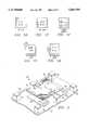
- One pixelgenerally denoted at 20, is basically a flap covering a shallow well and includes a silicon substrate 22, a spacer 24, a hinge layer 26, a pixel layer 28, a flap 30 formed in layers 26-28, and plasma etch access holds 32 in flap 30.
- the portion 34 of hinge layer 26 that in not covered by pixel layer 28forms a hinge attaching flap 30 to the portion of layers 26-28 supported by spacer 24.
- Pixel 20is fabricated using a robust semiconductor process upon silicon substrate 22.
- Spacer 24may be an insulating positive photoresist or other polymer
- hinge layer 26 and pixel layer 28are both an aluminum, titanium and silicon alloy (Ti: Si: Al), although these layers could also comprise of titanium tungsten, or other suitable materials.
- the hinge layer 34may be about 800 Angstroms thick, wherein the pixel 30 is much thicker to avoid cupping and warping, and may have a thickness of about 3,000 Angstroms.
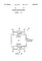
- Pixel 20is operably deflected by applying a voltage between mirror 30 and an underlying address electrode 36 defined on substrate 22. Flap 30 and the exposed surface of electrode 36 form the two plates of an air gap capacitor, and the opposite charges induced on the two plates by the applied voltage exert electrostatic force attracting flap 30 to substrate 22. This attractive force causes flap 30 to bend at hinge 34 and be deflected toward substrate 22. Depending on the opposing surface area of the electrodes, the spacing therebetween, the differential voltage applied, and the compliance of hinge 34, the degree of deflection of mirror 30 will vary. The deflection of mirror 30 is a function of the differential voltage, as graphically illustrated in FIG. 1C. As shown, the greater the differential voltage, that is, the greater the voltage applied to mirror 30, the greater the degree of deflection.
- this deflectionis nonlinear, and is not proportional to the voltage applied.
- a linear responsewhich may be the ideal response, is shown by the dotted line generally depicted at 38.
- the nonlinear relationshipis due to many reasons.
- the electrostatic forceis a function of the inverse of the square of the distance separating the mirror 30 and address electrode 36.
- the geometry and composition of the hingeaffects the compliance of hinge 34. The thickness of mirror 30 prevents significant warping, but the thinness of hinge 34 allows for large compliance.
- the deflection of flap 30is a highly nonlinear function of the applied voltage because the restoring force generated by the bending of hinge 34 is approximately a linear function of the deflection, but the electrostatic force of attraction increases as the distance between the closest corner of flap 30 and electrode 36 decreases. Recall that the capacitance increases as the distance decreases so the induced charges both increase in quantity and get closer together. As shown in FIG. 1C, the voltage at which mirror 30 becomes unstable and bends all the way to touch and short with electrode 36 is called the collapse voltage.
- the analog operating regionis that region between zero deflection and the collapsed situation.
- FIG. 1D-1Hillustrate equivalent alternative embodiments of the cantilever or leaf-type mirror 30 shown in FIG. 1.
- the present inventionachieves technical advantages as a spatial light modulator by providing a hexagon-shaped pixel supported by both a torsion hinge and at least one flexure hinge.
- the torsion hingesdefine the tilt axis
- the flexure hingesdefine the flat position and provide a restoring force to achieve enlarged stable range of tilt angles.
- the hexagon pixel structureallows the pixels to be tightly arranged in an array, the hexagon pixel geometry also being suitable to reflect circular light beams such as those from fiber optics.
- the present inventioncomprises a spatial light modulator of the type which includes a generally planar hexagonal light-reflecting pixel, i.e. mirror, which is deflectable out of a first, normal position into a plurality of second positions.
- a spatial light modulatorof the type which includes a generally planar hexagonal light-reflecting pixel, i.e. mirror, which is deflectable out of a first, normal position into a plurality of second positions.
- Light incident on the pixelis selectively modulated by being reflected from the pixel in selected directions, depending on the position of the pixel.
- the position of the pixelis dependent on a selected characteristic of an electrical signal, such as a voltage applied to an underlying address electrode.
- the deflection of the pixelstores potential mechanical energy in a pixel-supporting facility, this stored energy tending to return the pixel to the first, horizontal normal position.
- this pixel-supporting facilityincludes a first torsion hinge connected between the pixel and the first stationary post and defining a torsion axis. Deflection of the pixel effects its rotation about the torsional axis of the first hinge. At least one second flexure hinge is connected between the pixel and a second stationary post. Deflection of the pixel effects the flexure of the second hinge.
- deflection of the pixelis controllable for a large deflection range, and approximately proportional to the electrical signal applied to the underlining address circuit, preferably being an electrode.
- the pixelis monostable and cannot collapse on the address electrode, unless of course, large address voltages are provided.
- the hexagonal geometry of the pixelis suited to reflect circular light beams, such as those from fiber optics, while permitting a tightly packed arrangement of pixel mirrors. Excellent accuracy of the pixel mirror tilt angle for light steering is achieved, with the second hinge providing a well-defined undeflected (flat) position. Both the first hinge and the second hinge provide a restoration force.
- the points of connection of the first and second hinges to the pixelare separated about the perimeter of the pixel.
- the pixelhas a generally orthogonal profile, with the first hinge being connected to the pixel at a mid-point of a first side thereof.
- the second hingemay be connected to the first side of the pixel as well in one embodiment.
- the second hingemay be connected to the pixel proximate the juncture of the first side of pixel and a second side of the pixel.
- the second hingemay also be connected to the second side of the pixel including the most distal portion of the pixel, from the torsional axis.
- the torsional axis of the first hingeis generally co-planar with the pixel, and the second hinge in its unflexed state is oriented so as to be generally co-planar with the pixel and perpendicular to the torsional axis of the first hinge.
- the second hinge in its flexed statemay define a curved or slightly twisted surface at its corner, such that each end remains co-planar with the surface to which it is attached.
- the characteristic of the first hingeis such that the deflection of the pixel out of the first position is predominantly rotational about the torsion axis.
- the characteristic of the second hingeis such that the first position of the pixel is predominantly determined by the second hinge.
- the characteristics of both the hingesare such that the pixel is selectively deflectable out of the first position into a plurality of second positions determined by the selected characteristic of the electrical signal.
- the first and second hingesare respectively connected to the separated first and second posts. In an alternative embodiment, the first and second hinges may be connected to the same post.
- the pixelmay be reinforced to maintain flatness when undeflected, and when deflected out of the first position.
- the reinforcementmay comprise the perimeter of the pixel being corrugated or ridged to provided rigidity and minimize interfering with incident light being modulated.
- cupping of the pixelmay be minimized by providing radial corrugations or ridges.
- FIGS. 1A-1Hillustrate a prior art cantilever-type spatial light modulator, including a deflectable pixel deflectable as a function of an address voltage applied to an underlying address electrode;
- FIG. 2is a perspective view of a spatial light modulator according to the present invention including a deflectable pixel supported both by a torsion hinge, and at least one flexure hinge connected proximate the corners thereof;
- FIG. 3Ais a side view of the SLM of FIG. 2 with the torsion hinge posts removed, illustrating the pixel being deflected about the torsion hinge to steer incident light in a selected direction, the deflection of the pixel being a function of the voltage applied to the underlying address electrode;
- FIG. 3Bis a graph illustrating the linear deflection of the mirror as a function of the addressed voltage.
- FIG. 4is a top view of an alternative preferred embodiment of the pixel shown in FIG. 2, whereby the perimeter of the pixel is reinforced to insure the pixel is flat, rigid, and remains unflexed, even when pivoted about the torsional axis;
- FIG. 5is a cross section taken along line 5--5 in FIG. 4, illustrating the reinforcing structure of the pixel comprising the pixel being corrugated about the perimeter;
- FIG. 6is a top view of yet another alternative preferred embodiment wherein the torsion hinges and flexure hinges are supported by a common post;
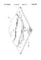
- FIG. 7is a perspective view of a spatial light modulator according to an alternative preferred embodiment of the invention including a hexagon-shaped pixel supported by a pair of torsion hinges, and a pair of flexure hinges;
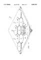
- FIG. 8is a top view of an array of hexagon shaped pixels of FIG. 7 illustrating the tightly packed arrangement of the pixels
- FIG. 9is a perspective view of a spatial light modulator according to another alternative preferred embodiment of the invention including an hexagon-shaped pixel elevated and overlapping underlying support superstructure;
- FIG. 10is a partial cross section of the pixel shown in FIG. 9, illustrating the hexagon mirror supported by the underlying yoke.
- FIG. 11is a perspective view of an array of pixels comprised of pixels shown in FIG. 9.
- SLM 40a monostable spatial light modulator according to the preferred embodiment of the present invention.
- SLM 40is well suited to operate in the analog mode to selectively steer incident light in a direction being a function of an electrical input.
- the deflection of the SLMmay be generally linear or nonlinear, as a function of the input electrical signal.
- the pixelresists collapse on its underlying address electrode due to the unique combination of hinges.
- SLM 40is a micromechanical structure formed using robust semiconductor processing.
- SLM 40is seen to comprise a generally rectangular reflective aluminum pixel 42 being supported along its mid section by a pair of torsional hinges 44.
- Hinges 44essentially bisect the mirror 42 and define a torsional axis therealong.
- Mirror 42is also seen to be supported proximate each corner thereof by an L-shaped flexure-type hinge 48.
- Torsional hinges 44extend from and are supported by a respective electrically conductive post 50, with the flexure hinges 48 being supported by a respective electrically conductive post 54.
- Each of posts 50 and 54are supported upon a silicon substrate 56, this substrate 56 also supporting a pair of electrically conductive address electrodes 60.
- Hinges 44connect to mirror 42 in a pair of opposed notches 58, notches 58 permitting long and compliant hinges 44. While the hinges, mirror and support posts are preferably comprised of electrically conductive material, each or all could also be comprised of electrically non-conductive material with the pixel having a light-reflective coating if desired. Hinges 48 could also have a serpentine shape, or be linear if desired. Hinges 48 could connect to pixel mirror 42 or either side proximate the corner of the adjoining sides, and limitation to the illustrated shapes of hinges 48 is not to be inferred.
- the angular deflection of mirror 42 about the torsional axis defined by hinges 44is seen to be a function of the voltage potential applied to one of the address electrodes 60.
- this voltage potentialinduces an electrostatic attraction between the mirror 42 and the underlying address electrode 60, thus creating an angular deflection of mirror 42, as shown.
- Torsional hinges 44rotate or twist with mirror 42 and provide restoring force in the form of a mechanical energy.
- Each of the four flexure hinges 48also provide a restoring force, and deform or flex, as shown, when mirror 42 deflects about the torsional axis defined by hinges 44.
- Hinges 48also provide restoring force in the form of mechanical energy, and define a normal flat or undeflected position when no voltage potential exists.
- torsional hinges 44are preferably comprised of a compliant material such as aluminum, an aluminum alloy or titanium tungsten, each having a thickness of about 500 Angstroms.
- Each of flexure hinges 48are also comprised of a compliant metal, such as aluminum, an aluminum alloy, or titanium tungsten, each having a thickness of about 500 Angstroms.
- the length of each hinge 48is approximately 10 microns.
- Each hinge 48extends from the respective post 54 a substantial length towards a respective torsional hinge 44 and is perpendicular therewith.
- Each flexure hinge 48has a 90° bend proximate mirror 42, and is connected to the corner of pixel 42, at the juncture of two adjacent sides, as shown.
- hinge 48The short segment of hinge 48 insures that a majority of the flexure of hinge 48 is along the major length, with any twisting taking place at the corner thereof.
- the hinge 48being about 500 Angstroms in thickness and having a length of about 10 microns, the flexure of these hinges permits mirror 42 to deflect as a function of the voltage potential provided to one address electrode 60, as shown in FIG. 3A.
- the spacing of mirror 42 from electrodes 60is about 1-10 microns.
- This analog operating rangeis represented as angle ⁇ , as shown in FIG. 3A. This corresponds to an input voltage of between 0 and 20 volts.
- As pixel 42 deflects angle ⁇ , incident lightis steered through a range of 2 ⁇ , as shown in FIG. 3A.
- the angular range that incident light can be reflectedis double the angular deflection of the pixel 42.
- pixel 42can be deflected with a linear or non-linear response, depending on the design, up to angle being about 10°.
- the range of steering lightis 20°.
- the response curve of mirror 42 as a function of address voltageis shown in FIG. 3B.
- mirror 42is deflected proportional to the address voltage.
- SLM 40When SLM 40 is operated as an optical switch or light steerer, incident light can be precisely steered to a receiver such as an optical sensor or scanner.
- the mirror tilt anglecan be achieved with a excellent accuracy for pixel steering.
- the torsion hinges 44define the tilt axis, whereby the flexure hinges 48 help achieve a controlled response and maintain mirror levelness when not addressed (undeflected). Both the torsion hinges and flexure hinges provide a mechanical restoration force and achieve a stable tilt range.
- FIG. 4a top view of an alternative preferred embodiment of the present invention is shown as SLM 70, with a modified mirror 72 is shown, wherein like numerals refer to like elements of the first embodiment.
- the perimeter of mirror 72is reinforced. This reinforcement preferably is achieved by corrugating the perimeter of the mirror, shown as a trench shown at 74.
- FIG. 5a cross section of mirror 42 taken along line 5--5 in FIG. 4 illustrates how mirror 42 is corrugated about the perimeter thereof.
- the trench 74 in the metalis one reliable way to reinforce mirror 72 to prevent warping or cupping, even when deflected about the torsion axis.
- Other equivalent methods of reinforcingcould include increasing the thickness of mirror 72 about the perimeter thereof, like a rib or ridge, and grid:
- FIG. 6another alternative embodiment of the present invention is shown, as SLM 80, wherein like numerals refer to like elements.
- Each of flexure hinges 82are connected to one of posts 84 from which torsion hinges 86 extend.
- This embodimentrequires only two support posts as compared to the six support posts shown in FIG. 2.
- each of the flexure hinges 82extend from the respective posts 84 and connect to one corner of mirror 72, proximate the juncture of two adjacent sides. All the hinges provide a restoration force to return the mirror to a flat, undeflected state when no address voltage is applied to address electrode 60.
- This embodimentpermits a higher fraction of optically active surfaces since SLM elements can be placed closer together.
- Pixel 90is seen to have a hexagonal shaped mirror 92 supported by a pair of torsion hinges 94 over a pair of addressing electrodes 96 and 98.
- Each of the hinges 94is supported by a support post 100 extending upward from a substrate 102.
- Also supporting mirror 98is a pair of arcuately shaped flexure hinges 106.
- Each of flexure hinges 106is connected to the distal end of mirror 92 at location 108, by a respective member 110.
- Each member 110perpendicularly extends from the distal end of mirror 92 each side of the torsion axis defined by hinges 94.
- Each of hinges 106is supported at each end by a support post 114 also extending upwardly from substrate 102, as shown.
- Pixel 90is similar to pixels 40 and 70 as shown in FIG. 2 and FIG. 4, respectively, in that the pixel mirror is supported by both the torsion hinges and flexure hinges.
- the torsion hinges 94define a torsion axis of rotation, whereby flexure hinges 106 limit the downward flexure of mirror 92 toward either of the addressed electrodes 96 and 98.
- the geometry of the hexagonal mirror 92allows the pixels 90 to be arranged in a tightly packed arrangement, such as that shown in FIG. 8.
- the length of flexure hinges 106are substantially longer than the length of torsion hinges 94 to provide good flexibility in the hinges 106 and facilitate rotation of the mirror 92 about the torsion axis. the flexure hinges 106 limit the deflection of mirror 92 to prevent shorting of the mirror 92 to the underlying address electrodes 96 and 98.
- each of the pixels 90has a hexagon-shaped mirror 92 oriented to be closely packed with another pixel 90, as shown.
- the hexagonal geometry of each mirror 92closely resembles that of a circle, and is ideally suited to reflect and modulate a beam of light having a circular cross section, such as that from fiber optic devices.
- the advantage of the hexagonal shape of mirrors 92is two fold. First, it facilitates the tightly packed arrangement shown in FIG. 8, and secondly, has a nearly circular surface area to reflect a circular beam of incident light. None of the light-reflecting surface of mirror 92 is wasted, that is, almost the entire surface area of mirror 92 receives and reflects incident light efficiently.
- Pixel 130is seen to include an elevated hexagonal shaped mirror 132 which substantially encompasses the underlying support structure.
- FIG. 10there is shown a partial cut away view of Pixel 130 to illustrate the underlying yoke 134 which is supported by torsion hinges 94.
- Yoke 134is the same size and profile as mirror 92 in FIG. 7, but does not necessarily need a reflective surface.
- Mirror 132is supported upon and over yoke 134 by a mirror post 136.
- Pixel 130in effect, has a hidden-hinge support superstructure, such as shown in FIG. 10.
- pixels 130 of an array generally shown at 140are very tightly packed, allowing for a high density arrangement of pixels 130 with no exposed underlying superstructure.
- the perimeter edges of pixel mirror 132extend closely proximate, but spaced from, corresponding edges of the adjacent pixel mirrors 132.
- the pixels 130are arranged close enough to one another so as to substantially reduce the possibilities of any incident light from impinging upon and defracting from the underlying support structure of the pixels, such as the torsion hinges 94 or the flexure hinges 106 shown in FIG. 10.
- the torsion hinges 94establish the torsion axis about which the yoke 134 and mirror 132 is rotated about, whereby the flexure hinges 106 restrict the rotational deflection of the yoke 134, and hence the mirror 132, about the torsion axis.
- an improved monostable spatial light modulatoris disclosed that is well suited to operate in the analog mode. Deflection of the pixel is proportional to an electrical signal applied to an underlying address electrode. The deflection and response of the pixel is selectable throughout a large range of applied address voltages. Thus, an incident light beam can be precisely steered to a receiver, such as a sensor or a light scanner. Given the tight process parameter tolerances of conventional semiconductor processing, spatial light modulators with repeatable operating characteristics can be manufactured. The flexure hinges ensure the mirror will resist collapse, contribute to the monostable analog operating characteristics of the mirror, provide a restoring force, and establish mirror levelness in the unaddressed situation.
- the torsional hingesdefine the tilt axis, and also provide a restoring force.
- the present inventioncan be manufactured using robust manufacturing processes utilized in manufacturing monolithic integrated circuits.
- the present inventionis inexpensive, light weight, and requires low drive power.
- the deflection speed of the deviceis very high, with response time of the mirror deflection well suited for high speed optical switching.
- the surface area of the mirrorcan be custom designed to have a very small size, such as 17 microns square, but can be relatively large if desired to provide a large area flat pixel for steering large-area light beams.
- the pixelmay have a hexagon-shaped geometry to optically switch an incident circular light beam, such as from fiber optics, and which can be tightly packed in an array of pixels.
Landscapes
- Physics & Mathematics (AREA)
- Engineering & Computer Science (AREA)
- Computer Hardware Design (AREA)
- Microelectronics & Electronic Packaging (AREA)
- General Physics & Mathematics (AREA)
- Optics & Photonics (AREA)
- Mechanical Light Control Or Optical Switches (AREA)
- Mounting And Adjusting Of Optical Elements (AREA)
Abstract
Description
Cross reference is made to the following commonly-assigned co-pending patent applications, the teachings of which are incorporated herein by reference.
______________________________________ Ser. No. TITLE FILING DATE ______________________________________ 08/414,831 Spatial Light Modulator with 03-31-95 Superstructure Light Shield 08/097,824 Microminiature, Monolithic, 07-27-93 Variable Electrical Device and Apparatus Including Same 08/424,021 Active Yoke Hidden Hinge 04-18-95 Digital Micromirror Device 08/171,303 Multi-Level Digital Micromirror 12-21-93 Device 08/482,477 Method and Device for Multi- 06-07-95 Format Television 08/455,475 Spatial Light Modulator Having an Analog Beam for Steering Light 08/424,021 Active Yoke Hidden Hinge 04-18-95 Digital Micromirror Device ______________________________________
The present invention is generally related to spatial light modulators for modulating incident light and suitable as an optical switch, and more particularly, to a device having a selectively deflectable mirror being supported by at least one hinge for steering incident light in a direction being a function of the degree to which the mirror is deflected.
Spatial light modulators (SLM's) have found numerous applications in the areas of optical information processing, projection displays, video and graphics monitors, televisions, and electrostatic printing. SLM's have also found uses as optical switches, optical shutters, light valves, pixel steerers and so forth. SLM's are devices that modulate incident light in a spatial pattern to form a light image corresponding to an electrical or optical input. The incident light may be modulated in its phase, intensity, polarization, and/or direction. The light modulation may be achieved by a variety of materials exhibiting various electro-optic or magneto-optic effects, and by materials that modulate light by surface deformation.
The present invention relates to SLM's of the foregoing type which may be used in a variety of devices, including light switches, light valves, pixel steerers and optical shutters.
A recent innovation of Texas Instrument Incorporated of Dallas, Tex. is the digital micromirror device or deformable mirror device, collectively known as the DMD. The DMD is a spatial light modulator comprising a monolithic single-chip integrated circuit, typically having a high density array of 17 micron square deflectable micromirrors but may have other dimensions. These mirrors are fabricated over address circuitry including an array of memory cells and address electrodes. The mirrors may be bistable and be operated in the digital mode, the mirror being stable in one of two deflected positions. A source of light directed upon the mirror is reflected in one of two directions by the mirror. When used in the digital mode, incident light from the army of mirrors can be modulated and directed to a projector lens and then focused on a display screen or a photoreceptor drum to form a light image. When the mirror is in one position, known as the "on" position, light is directed into the projector lens. In the other position, known as the "off" mirror position, light is directed to a light absorber. The DMD may also be monostable and operated in the analog mode, and finds use as a light switch, pixel steerer, optical shutter, scanner, and the like.
For a more detailed discussion of the DMD device and systems incorporating the device, cross reference is made to U.S. Pat. No. 5,061,049 to Hornbeck, entitled "Spatial Light Modulator and Method"; U.S. Pat. No. 5,079,544 to DeMond, et al, entitled "Standard Independent Digitized Video System"; and U.S. Pat. No. 5,105,369 to Nelson, entitled "Printing System Exposure Module Alignment Method and Apparatus of Manufacture", each patent being assigned to the same assignee of the present invention, and the teachings of each are incorporated herein by reference. Gray scale of the pixels forming the image may be achieved by pulse width modulation techniques of the mirrors, such as that described in U.S. Pat. No. 5,278,652, entitled "DMD Architecture and Timing for Use in a Pulse-Width Modulated Display System", assigned to the same assignee of the present invention, and the teachings of each are incorporated herein by reference.
Commonly assigned U.S. Pat. No. 4,662,746 to Hornbeck entitled "Spatial Light Modulator and Method", U.S. Pat. No. 4,710,732 to Hornbeck entitled "Spatial Light Modulator and Method", U.S. Pat. No. 4,956,619 to Hornbeck entitled "Spatial Light Modulator", and U.S. Pat. No. 5,172,262 to Hornbeck entitled "Spatial Light Modulator and Method" disclose various structures and methods of producing micro mechanical devices, specifically, monostable DMD SLM's suited for use in the analog mode, the teachings of each incorporated herein by reference.
Commonly assigned U.S. Pat. No. 5,096,279 to Hornbeck et al. entitled "Spatial Light Modulator and Method", U.S. Pat. No. 5,142,405 to Hornbeck entitled "Bistable DMD Addressing Circuit and Method", and U.S. Pat. No. 5,212,582 to Nelson entitled "Electrostatically Controlled Pixel Steering Device and Method" disclose various structures and methods for producing the same that are bistable and suited for use in the digital mode, the teachings of each incorporated herein by reference.
Referring to FIGS. 1A-1H, these embodiments being disclosed in a commonly assigned U.S. Pat. No. 5,172,262, there is shown a monostable DMD spatial light modulator that can be operated in the analog mode. One pixel, generally denoted at 20, is basically a flap covering a shallow well and includes asilicon substrate 22, aspacer 24, ahinge layer 26, apixel layer 28, aflap 30 formed in layers 26-28, and plasma etch access holds 32 inflap 30. Theportion 34 ofhinge layer 26 that in not covered bypixel layer 28 forms ahinge attaching flap 30 to the portion of layers 26-28 supported byspacer 24.Pixel 20 is fabricated using a robust semiconductor process uponsilicon substrate 22.Spacer 24 may be an insulating positive photoresist or other polymer,hinge layer 26 andpixel layer 28 are both an aluminum, titanium and silicon alloy (Ti: Si: Al), although these layers could also comprise of titanium tungsten, or other suitable materials. Thehinge layer 34 may be about 800 Angstroms thick, wherein thepixel 30 is much thicker to avoid cupping and warping, and may have a thickness of about 3,000 Angstroms.
As also illustrated in FIG. 1C, this deflection is nonlinear, and is not proportional to the voltage applied. A linear response, which may be the ideal response, is shown by the dotted line generally depicted at 38. The nonlinear relationship is due to many reasons. First, the electrostatic force is a function of the inverse of the square of the distance separating themirror 30 andaddress electrode 36. Secondly, the geometry and composition of the hinge affects the compliance ofhinge 34. The thickness ofmirror 30 prevents significant warping, but the thinness ofhinge 34 allows for large compliance. The deflection offlap 30 is a highly nonlinear function of the applied voltage because the restoring force generated by the bending ofhinge 34 is approximately a linear function of the deflection, but the electrostatic force of attraction increases as the distance between the closest corner offlap 30 andelectrode 36 decreases. Recall that the capacitance increases as the distance decreases so the induced charges both increase in quantity and get closer together. As shown in FIG. 1C, the voltage at whichmirror 30 becomes unstable and bends all the way to touch and short withelectrode 36 is called the collapse voltage. The analog operating region is that region between zero deflection and the collapsed situation.
FIG. 1D-1H illustrate equivalent alternative embodiments of the cantilever or leaf-type mirror 30 shown in FIG. 1.
When operating a spatial light modulator, such as of the type just discussed and referenced in FIG. 1A-1H, it may be desired to operated the deflectable member in the analog region, whereby the angle of deflection ofmirror 30 is linearly proportional to the voltage applied. To operate the device as a light beam steerer, scanner, or light switch, it is desirable to precisely control the degree of deflection as so to precisely steer incident light to a receiver, such as a sensor. Therefore, in prior art designs, such as that shown in FIGS. 1A-1H, it is imperative that a repeatable process be followed. In the practical world, however, process tolerances allow for some deviation form device to device. Thus, for a given voltage being applied to addresselectrode 36, the deflection ofmirror 30 from device to device will vary slightly. Consequently, characterization of the device prior to implementation is necessary when the device is used in the analog mode.
It is desired to provide a spatial light modulator suitable for use as an optical switch with a deflectable pixel well suited to be used in the analog mode.
The present invention achieves technical advantages as a spatial light modulator by providing a hexagon-shaped pixel supported by both a torsion hinge and at least one flexure hinge. The torsion hinges define the tilt axis, and the flexure hinges define the flat position and provide a restoring force to achieve enlarged stable range of tilt angles. Through the combination of these hinges, the pixel is nearly monostable and will resist collapse. The hexagon pixel structure allows the pixels to be tightly arranged in an array, the hexagon pixel geometry also being suitable to reflect circular light beams such as those from fiber optics.
The present invention comprises a spatial light modulator of the type which includes a generally planar hexagonal light-reflecting pixel, i.e. mirror, which is deflectable out of a first, normal position into a plurality of second positions. Light incident on the pixel is selectively modulated by being reflected from the pixel in selected directions, depending on the position of the pixel. The position of the pixel is dependent on a selected characteristic of an electrical signal, such as a voltage applied to an underlying address electrode. The deflection of the pixel stores potential mechanical energy in a pixel-supporting facility, this stored energy tending to return the pixel to the first, horizontal normal position. Preferably, this pixel-supporting facility includes a first torsion hinge connected between the pixel and the first stationary post and defining a torsion axis. Deflection of the pixel effects its rotation about the torsional axis of the first hinge. At least one second flexure hinge is connected between the pixel and a second stationary post. Deflection of the pixel effects the flexure of the second hinge. By providing two types of hinges, deflection of the pixel is controllable for a large deflection range, and approximately proportional to the electrical signal applied to the underlining address circuit, preferably being an electrode. The pixel is monostable and cannot collapse on the address electrode, unless of course, large address voltages are provided. The hexagonal geometry of the pixel is suited to reflect circular light beams, such as those from fiber optics, while permitting a tightly packed arrangement of pixel mirrors. Excellent accuracy of the pixel mirror tilt angle for light steering is achieved, with the second hinge providing a well-defined undeflected (flat) position. Both the first hinge and the second hinge provide a restoration force.
The points of connection of the first and second hinges to the pixel are separated about the perimeter of the pixel. The pixel has a generally orthogonal profile, with the first hinge being connected to the pixel at a mid-point of a first side thereof. The second hinge may be connected to the first side of the pixel as well in one embodiment. The second hinge may be connected to the pixel proximate the juncture of the first side of pixel and a second side of the pixel. The second hinge may also be connected to the second side of the pixel including the most distal portion of the pixel, from the torsional axis. The torsional axis of the first hinge is generally co-planar with the pixel, and the second hinge in its unflexed state is oriented so as to be generally co-planar with the pixel and perpendicular to the torsional axis of the first hinge. The second hinge in its flexed state may define a curved or slightly twisted surface at its corner, such that each end remains co-planar with the surface to which it is attached.
The characteristic of the first hinge is such that the deflection of the pixel out of the first position is predominantly rotational about the torsion axis. The characteristic of the second hinge is such that the first position of the pixel is predominantly determined by the second hinge. The characteristics of both the hinges are such that the pixel is selectively deflectable out of the first position into a plurality of second positions determined by the selected characteristic of the electrical signal. The first and second hinges are respectively connected to the separated first and second posts. In an alternative embodiment, the first and second hinges may be connected to the same post. The pixel may be reinforced to maintain flatness when undeflected, and when deflected out of the first position. Preferably, the reinforcement may comprise the perimeter of the pixel being corrugated or ridged to provided rigidity and minimize interfering with incident light being modulated. Alternatively or additionally, cupping of the pixel may be minimized by providing radial corrugations or ridges.
FIGS. 1A-1H illustrate a prior art cantilever-type spatial light modulator, including a deflectable pixel deflectable as a function of an address voltage applied to an underlying address electrode;
FIG. 2 is a perspective view of a spatial light modulator according to the present invention including a deflectable pixel supported both by a torsion hinge, and at least one flexure hinge connected proximate the corners thereof;
FIG. 3A is a side view of the SLM of FIG. 2 with the torsion hinge posts removed, illustrating the pixel being deflected about the torsion hinge to steer incident light in a selected direction, the deflection of the pixel being a function of the voltage applied to the underlying address electrode;
FIG. 3B is a graph illustrating the linear deflection of the mirror as a function of the addressed voltage.
FIG. 4 is a top view of an alternative preferred embodiment of the pixel shown in FIG. 2, whereby the perimeter of the pixel is reinforced to insure the pixel is flat, rigid, and remains unflexed, even when pivoted about the torsional axis;
FIG. 5 is a cross section taken alongline 5--5 in FIG. 4, illustrating the reinforcing structure of the pixel comprising the pixel being corrugated about the perimeter;
FIG. 6 is a top view of yet another alternative preferred embodiment wherein the torsion hinges and flexure hinges are supported by a common post;
FIG. 7 is a perspective view of a spatial light modulator according to an alternative preferred embodiment of the invention including a hexagon-shaped pixel supported by a pair of torsion hinges, and a pair of flexure hinges;
FIG. 8 is a top view of an array of hexagon shaped pixels of FIG. 7 illustrating the tightly packed arrangement of the pixels;
FIG. 9 is a perspective view of a spatial light modulator according to another alternative preferred embodiment of the invention including an hexagon-shaped pixel elevated and overlapping underlying support superstructure;
FIG. 10 is a partial cross section of the pixel shown in FIG. 9, illustrating the hexagon mirror supported by the underlying yoke; and
FIG. 11 is a perspective view of an array of pixels comprised of pixels shown in FIG. 9.
Referring to FIG. 2, there is generally shown at 40 a monostable spatial light modulator according to the preferred embodiment of the present invention.SLM 40 is well suited to operate in the analog mode to selectively steer incident light in a direction being a function of an electrical input. The deflection of the SLM may be generally linear or nonlinear, as a function of the input electrical signal. The pixel resists collapse on its underlying address electrode due to the unique combination of hinges.
Referring to FIG. 3A the angular deflection ofmirror 42 about the torsional axis defined byhinges 44 is seen to be a function of the voltage potential applied to one of theaddress electrodes 60. With a bias voltage being applied to mirror 42 viaposts 54 and hinges 48, and an address potential being applied to one of the twoaddress electrodes 60, this voltage potential induces an electrostatic attraction between themirror 42 and theunderlying address electrode 60, thus creating an angular deflection ofmirror 42, as shown. Torsional hinges 44 rotate or twist withmirror 42 and provide restoring force in the form of a mechanical energy. Each of the four flexure hinges 48 also provide a restoring force, and deform or flex, as shown, whenmirror 42 deflects about the torsional axis defined by hinges 44.Hinges 48 also provide restoring force in the form of mechanical energy, and define a normal flat or undeflected position when no voltage potential exists.
By way of illustration but with no limitation to the following dimensions or shapes, torsional hinges 44 are preferably comprised of a compliant material such as aluminum, an aluminum alloy or titanium tungsten, each having a thickness of about 500 Angstroms. Each of flexure hinges 48 are also comprised of a compliant metal, such as aluminum, an aluminum alloy, or titanium tungsten, each having a thickness of about 500 Angstroms. The length of eachhinge 48 is approximately 10 microns. Eachhinge 48 extends from the respective post 54 a substantial length towards a respectivetorsional hinge 44 and is perpendicular therewith. Eachflexure hinge 48 has a 90° bendproximate mirror 42, and is connected to the corner ofpixel 42, at the juncture of two adjacent sides, as shown. The short segment ofhinge 48 insures that a majority of the flexure ofhinge 48 is along the major length, with any twisting taking place at the corner thereof. With thehinge 48 being about 500 Angstroms in thickness and having a length of about 10 microns, the flexure of these hinges permits mirror 42 to deflect as a function of the voltage potential provided to oneaddress electrode 60, as shown in FIG. 3A. The spacing ofmirror 42 fromelectrodes 60 is about 1-10 microns. This analog operating range is represented as angle θ, as shown in FIG. 3A. This corresponds to an input voltage of between 0 and 20 volts. Aspixel 42 deflects angle θ, incident light is steered through a range of 2θ, as shown in FIG. 3A. As expected due to optical light properties, the angular range that incident light can be reflected is double the angular deflection of thepixel 42. In the present invention,pixel 42 can be deflected with a linear or non-linear response, depending on the design, up to angle being about 10°. Thus, the range of steering light is 20°. The response curve ofmirror 42 as a function of address voltage is shown in FIG. 3B.
With an address voltage being applied to oneaddress electrode 60 being from 0 to 20 volts,mirror 42 is deflected proportional to the address voltage. WhenSLM 40 is operated as an optical switch or light steerer, incident light can be precisely steered to a receiver such as an optical sensor or scanner. The mirror tilt angle can be achieved with a excellent accuracy for pixel steering. The torsion hinges 44 define the tilt axis, whereby the flexure hinges 48 help achieve a controlled response and maintain mirror levelness when not addressed (undeflected). Both the torsion hinges and flexure hinges provide a mechanical restoration force and achieve a stable tilt range. With two flexure hinges 48 being provided each side of the torsion axis, there is little possibility of a collapsed mirror, unless one of the hinges should break, which is not likely given the range of operable address voltages provided to addresselectrode 60. Compliance of each offlexure 48 and torsion hinges 44 is excellent.
Referring now to FIG. 4, a top view of an alternative preferred embodiment of the present invention is shown asSLM 70, with a modifiedmirror 72 is shown, wherein like numerals refer to like elements of the first embodiment. To ensure thatmirror 72 remains fiat and does not warp, even in an extreme deflected state, the perimeter ofmirror 72 is reinforced. This reinforcement preferably is achieved by corrugating the perimeter of the mirror, shown as a trench shown at 74. Referring to FIG. 5, a cross section ofmirror 42 taken alongline 5--5 in FIG. 4 illustrates howmirror 42 is corrugated about the perimeter thereof. Thetrench 74 in the metal is one reliable way to reinforcemirror 72 to prevent warping or cupping, even when deflected about the torsion axis. Other equivalent methods of reinforcing could include increasing the thickness ofmirror 72 about the perimeter thereof, like a rib or ridge, and grid:
Referring now to FIG. 6, another alternative embodiment of the present invention is shown, asSLM 80, wherein like numerals refer to like elements. Each of flexure hinges 82 are connected to one ofposts 84 from which torsion hinges 86 extend. This embodiment requires only two support posts as compared to the six support posts shown in FIG. 2. Again, each of the flexure hinges 82 extend from therespective posts 84 and connect to one corner ofmirror 72, proximate the juncture of two adjacent sides. All the hinges provide a restoration force to return the mirror to a flat, undeflected state when no address voltage is applied to addresselectrode 60. This embodiment permits a higher fraction of optically active surfaces since SLM elements can be placed closer together.
Referring now to FIG. 7, there is generally shown at 90 a pixel according to another alternative preferred embodiment of the present invention.Pixel 90 is seen to have a hexagonal shapedmirror 92 supported by a pair of torsion hinges 94 over a pair of addressingelectrodes hinges 94 is supported by asupport post 100 extending upward from asubstrate 102. Also supportingmirror 98 is a pair of arcuately shaped flexure hinges 106. Each of flexure hinges 106 is connected to the distal end ofmirror 92 atlocation 108, by arespective member 110. Eachmember 110 perpendicularly extends from the distal end ofmirror 92 each side of the torsion axis defined by hinges 94. Each ofhinges 106 is supported at each end by asupport post 114 also extending upwardly fromsubstrate 102, as shown.
Referring now to FIG. 8, there is shown a spatial light modulator pixel array generally shown at 120. As shown, each of thepixels 90 has a hexagon-shapedmirror 92 oriented to be closely packed with anotherpixel 90, as shown. In addition, the hexagonal geometry of eachmirror 92 closely resembles that of a circle, and is ideally suited to reflect and modulate a beam of light having a circular cross section, such as that from fiber optic devices. Thus, the advantage of the hexagonal shape ofmirrors 92 is two fold. First, it facilitates the tightly packed arrangement shown in FIG. 8, and secondly, has a nearly circular surface area to reflect a circular beam of incident light. None of the light-reflecting surface ofmirror 92 is wasted, that is, almost the entire surface area ofmirror 92 receives and reflects incident light efficiently.
Referring now to FIG. 9, there is shown generally at 130 a pixel according to yet another alternative preferred embodiment of the present invention.Pixel 130 is seen to include an elevated hexagonal shapedmirror 132 which substantially encompasses the underlying support structure. Referring to FIG. 10, there is shown a partial cut away view ofPixel 130 to illustrate theunderlying yoke 134 which is supported by torsion hinges 94.Yoke 134 is the same size and profile asmirror 92 in FIG. 7, but does not necessarily need a reflective surface.Mirror 132 is supported upon and overyoke 134 by amirror post 136.Pixel 130, in effect, has a hidden-hinge support superstructure, such as shown in FIG. 10.
The advantages of this embodiment can be appreciated in view of FIG. 11, wherebypixels 130 of an array generally shown at 140 are very tightly packed, allowing for a high density arrangement ofpixels 130 with no exposed underlying superstructure. The perimeter edges ofpixel mirror 132 extend closely proximate, but spaced from, corresponding edges of the adjacent pixel mirrors 132. Thepixels 130 are arranged close enough to one another so as to substantially reduce the possibilities of any incident light from impinging upon and defracting from the underlying support structure of the pixels, such as the torsion hinges 94 or the flexure hinges 106 shown in FIG. 10. Again, the torsion hinges 94 establish the torsion axis about which theyoke 134 andmirror 132 is rotated about, whereby the flexure hinges 106 restrict the rotational deflection of theyoke 134, and hence themirror 132, about the torsion axis.
For additional discussion and teaching how to fabricate thepixels 130, cross reference is made to commonly assigned co-pending patent application Ser. No. 08/424,021, entitled "Active Yoke Hidden Hinge digital Micromirror Device", which details the hidden hinge structure, the teachings of which incorporated herein by reference.
In summary, an improved monostable spatial light modulator is disclosed that is well suited to operate in the analog mode. Deflection of the pixel is proportional to an electrical signal applied to an underlying address electrode. The deflection and response of the pixel is selectable throughout a large range of applied address voltages. Thus, an incident light beam can be precisely steered to a receiver, such as a sensor or a light scanner. Given the tight process parameter tolerances of conventional semiconductor processing, spatial light modulators with repeatable operating characteristics can be manufactured. The flexure hinges ensure the mirror will resist collapse, contribute to the monostable analog operating characteristics of the mirror, provide a restoring force, and establish mirror levelness in the unaddressed situation. The torsional hinges define the tilt axis, and also provide a restoring force. The present invention can be manufactured using robust manufacturing processes utilized in manufacturing monolithic integrated circuits. The present invention is inexpensive, light weight, and requires low drive power. The deflection speed of the device is very high, with response time of the mirror deflection well suited for high speed optical switching. The surface area of the mirror can be custom designed to have a very small size, such as 17 microns square, but can be relatively large if desired to provide a large area flat pixel for steering large-area light beams. The pixel may have a hexagon-shaped geometry to optically switch an incident circular light beam, such as from fiber optics, and which can be tightly packed in an array of pixels.
Though the invention has been described with respect to a specific preferred embodiment, many variations and modifications will become apparent to those skilled in the art upon reading the present application. It is therefore the intention that the appended claims be interpreted as broadly as possible in view of the prior art to include all such variations and modifications.
Claims (16)
1. A spatial light modulator, comprising:
(a) at least one address electrode on a substrate;
(b) a hexagon-shaped light-reflective pixel positioned over said address electrode which is deflectable out of a first, normal position into a plurality of second positions, light incident on the pixel being selectively modulated by being reflected from the pixel in selected directions depending on the position of the pixel, the position of the pixel being dependent on a selected characteristic of an electrical signal provided to said underlying address electrode;
(c) a first torsion member connected between the pixel and a first stationary post and defining a torsion axis, deflection of the pixel effecting its rotation about the torsional axis of the first member; and
(d) a second flexure member connected between the pixel and a second stationary post, deflection of the pixel effecting flexure of the second member.
2. The modulator as set forth in claim 1, wherein:
the points of connection of the members to the pixel are separated about the periphery of the pixel.
3. The modulator as in claim 2, wherein:
the pixel has a generally orthogonal profile,
the first member is connected to the pixel at a mid-point of a first side thereof, and
the second member is connected to a second side of the pixel.
4. The modulator as in claim 3, wherein:
the second member is connected to the pixel proximate the juncture of the first side of the pixel and the second side of the pixel.
5. The modulator as in claim 2, wherein:
the second member in its unflexed state is oriented so as to be perpendicular to the torsional axis of the first member.
6. The modulator as in claim 5, wherein:
the second member in its flexed state defines a curved surface, the surface of which is generally perpendicular to the torsional axis of the first member.
7. The modulator as in claim 1, wherein:
the characteristics of the first member are such that the deflection of the pixel out of the first position is predominantly rotational about the torsion axis, and the characteristics of the second member are such that the first position of the pixel is predominantly determined by the second member.
8. The modulator as in claim 7, wherein:
the characteristics of the members are such that the pixel is selectively deflectable out of the first position into a plurality of the second positions determined by the voltage of the electrical signal.
9. The modulator as in claim 1, wherein:
the first and second members are respectively connected to separated said first and second posts.
10. The modulator as in claim 1, wherein:
the first and second members are connected to the same said posts.
11. The modulator as in claim 1, wherein:
the pixel is reinforced to maintain flatness.
12. The modulator as in claim 11, wherein:
the pixel is reinforced about a perimeter thereof.
13. The modulator as in claim 12, wherein:
the pixel is corrugated about the perimeter.
14. The modulator as in claim 11, wherein the pixel is radially reinforced from proximate a midsection thereof.
15. The modulator as in claim 1, wherein said pixel comprises a mirror elevated upon and over a yoke, said yoke being supported by said first and second members and said address electrode.
16. The modulator as in claim 1, wherein the length of said second flexure member is substantially longer than the length of said first torsion member.
Priority Applications (2)
| Application Number | Priority Date | Filing Date | Title |
|---|---|---|---|
| US08/537,179US5661591A (en) | 1995-09-29 | 1995-09-29 | Optical switch having an analog beam for steering light |
| JP8258376AJPH09127439A (en) | 1995-09-29 | 1996-09-30 | Optical switch with analog beam for optical operation |
Applications Claiming Priority (1)
| Application Number | Priority Date | Filing Date | Title |
|---|---|---|---|
| US08/537,179US5661591A (en) | 1995-09-29 | 1995-09-29 | Optical switch having an analog beam for steering light |
Publications (1)
| Publication Number | Publication Date |
|---|---|
| US5661591Atrue US5661591A (en) | 1997-08-26 |
Family
ID=24141545
Family Applications (1)
| Application Number | Title | Priority Date | Filing Date |
|---|---|---|---|
| US08/537,179Expired - LifetimeUS5661591A (en) | 1995-09-29 | 1995-09-29 | Optical switch having an analog beam for steering light |
Country Status (2)
| Country | Link |
|---|---|
| US (1) | US5661591A (en) |
| JP (1) | JPH09127439A (en) |
Cited By (174)
| Publication number | Priority date | Publication date | Assignee | Title |
|---|---|---|---|---|
| US5943157A (en)* | 1997-05-08 | 1999-08-24 | Texas Instruments Incorporated | Spatial light modulator having improved contrast ratio |
| EP0980014A1 (en)* | 1998-06-02 | 2000-02-16 | Texas Instruments Incorporated | Spring-ring micromechanical device |
| US6028690A (en)* | 1997-11-26 | 2000-02-22 | Texas Instruments Incorporated | Reduced micromirror mirror gaps for improved contrast ratio |
| US6044705A (en)* | 1993-10-18 | 2000-04-04 | Xros, Inc. | Micromachined members coupled for relative rotation by torsion bars |
| WO2000036452A1 (en)* | 1998-12-16 | 2000-06-22 | Robert Bosch Gmbh | Deflectable micro-mirror |
| US6091067A (en)* | 1998-06-02 | 2000-07-18 | Science Applications International Corporation | Scanning device using fiber optic bimorph |
| US6137105A (en)* | 1998-06-02 | 2000-10-24 | Science Applications International Corporation | Multiple parallel source scanning device |
| US6166756A (en)* | 1998-06-02 | 2000-12-26 | Science Applications International Corporation | Multiple channel data writing device |
| US6201631B1 (en)* | 1999-10-08 | 2001-03-13 | Lucent Technologies Inc. | Process for fabricating an optical mirror array |
| US6229640B1 (en) | 1999-08-11 | 2001-05-08 | Adc Telecommunications, Inc. | Microelectromechanical optical switch and method of manufacture thereof |
| US6242363B1 (en) | 1999-08-11 | 2001-06-05 | Adc Telecommunications, Inc. | Method of etching a wafer layer using a sacrificial wall to form vertical sidewall |
| US6246658B1 (en) | 1998-06-02 | 2001-06-12 | Science Applications International Corporation | Multiple channel scanning device using optoelectronic switching |
| US6271955B1 (en)* | 1995-12-01 | 2001-08-07 | Seiko Epson Corporation | Method of manufacturing spatial light modulator and electronic device employing it |
| US6285489B1 (en)* | 1999-08-05 | 2001-09-04 | Microvision Inc. | Frequency tunable resonant scanner with auxiliary arms |
| US6316282B1 (en) | 1999-08-11 | 2001-11-13 | Adc Telecommunications, Inc. | Method of etching a wafer layer using multiple layers of the same photoresistant material |
| US6341118B1 (en) | 1998-06-02 | 2002-01-22 | Science Applications International Corporation | Multiple channel scanning device using oversampling and image processing to increase throughput |
| US6351330B2 (en)* | 1998-04-10 | 2002-02-26 | Samsung Electronics Co., Ltd. | Micromirror device for image display apparatus |
| US6373619B1 (en)* | 1998-03-02 | 2002-04-16 | Micronic Laser Systems Ab | Pattern generator with improved address resolution |
| US6426013B1 (en) | 1993-10-18 | 2002-07-30 | Xros, Inc. | Method for fabricating micromachined members coupled for relative rotation |
| US6430333B1 (en)* | 1999-04-15 | 2002-08-06 | Solus Micro Technologies, Inc. | Monolithic 2D optical switch and method of fabrication |
| US20020109899A1 (en)* | 2001-01-18 | 2002-08-15 | Kouichi Ohtaka | Optical modulator, optical modulator manufacturing method, light information processing apparatus including optical modulator, image formation apparatus including optical modulator, and image projection and display appratus including optical modulator |
| US6437903B1 (en)* | 2002-02-20 | 2002-08-20 | Intel Corporation | Light modulator with two mirror sets |
| US20020122237A1 (en)* | 2001-03-01 | 2002-09-05 | Torbjorn Sandstrom | Method and apparatus for spatial light modulation |
| WO2002075426A1 (en) | 2001-02-07 | 2002-09-26 | Transparent Networks, Inc. | Microelectromechanical mirror and mirror array |
| US6467345B1 (en) | 1993-10-18 | 2002-10-22 | Xros, Inc. | Method of operating micromachined members coupled for relative rotation |
| US6469821B2 (en)* | 1999-12-28 | 2002-10-22 | Texas Instruments Incorporated | Micromirror structures for orthogonal illumination |
| US6473221B2 (en)* | 2000-11-02 | 2002-10-29 | Fujitsu Limited | Galvano-mirror and method of making the same |
| WO2002086585A1 (en)* | 2001-03-19 | 2002-10-31 | The Research Foundation Of State University Of New York | Mems-based optical switch wherein the mirrors comprise an optical sensor |
| US20030016906A1 (en)* | 2001-07-18 | 2003-01-23 | Nec Corporation | Optical switch |
| WO2001088595A3 (en)* | 2000-05-18 | 2003-01-30 | Calient Networks Inc | A micromachined apparatus for improved reflection of light |
| US6535091B2 (en)* | 2000-11-07 | 2003-03-18 | Sarnoff Corporation | Microelectronic mechanical systems (MEMS) switch and method of fabrication |
| US6556318B1 (en)* | 1998-07-20 | 2003-04-29 | At&T Corp. | Method and apparatus for signal and switch monitoring in an optical cross connect |
| US6556741B1 (en) | 2000-10-25 | 2003-04-29 | Omm, Inc. | MEMS optical switch with torsional hinge and method of fabrication thereof |
| US6560384B1 (en) | 2000-06-01 | 2003-05-06 | Calient Networks, Inc. | Optical switch having mirrors arranged to accommodate freedom of movement |
| US6567574B1 (en) | 2000-10-06 | 2003-05-20 | Omm, Inc. | Modular three-dimensional optical switch |
| US6584052B1 (en) | 1998-06-02 | 2003-06-24 | Science Applications International Corporation | Method and apparatus for controlling the focus of a read/write head for an optical scanner |
| EP1197778A3 (en)* | 2000-10-10 | 2003-07-16 | Agere Systems Guardian Corporation | Micro-electro-optical mechanical device having an implanted dopant included therein and a method of manufacture therefor |
| US6600587B2 (en)* | 2001-04-23 | 2003-07-29 | Memx, Inc. | Surface micromachined optical system with reinforced mirror microstructure |
| KR100398804B1 (en)* | 2001-03-05 | 2003-09-19 | 유승진 | Optical switch actuated with multiphase driving voltage |
| US6654158B2 (en) | 2001-04-20 | 2003-11-25 | Microvision, Inc. | Frequency tunable resonant scanner with auxiliary arms |
| US6657764B1 (en)* | 1999-03-18 | 2003-12-02 | The Trustees Of Boston University | Very large angle integrated optical scanner made with an array of piezoelectric monomorphs |
| US20030234994A1 (en)* | 2002-06-19 | 2003-12-25 | Pan Shaoher X. | Reflective spatial light modulator |
| US20040004753A1 (en)* | 2002-06-19 | 2004-01-08 | Pan Shaoher X. | Architecture of a reflective spatial light modulator |
| US20040008402A1 (en)* | 2000-08-11 | 2004-01-15 | Patel Satyadev R. | Micromirrors with mechanisms for enhancing coupling of the micromirrors with electrostatic fields |
| US20040070813A1 (en)* | 2002-10-11 | 2004-04-15 | Aubuchon Christopher M. | Micromirror systems with electrodes configured for sequential mirror attraction |
| US20040069742A1 (en)* | 2002-06-19 | 2004-04-15 | Pan Shaoher X. | Fabrication of a reflective spatial light modulator |
| US20040085617A1 (en)* | 2002-11-01 | 2004-05-06 | Microvision, Inc. | Frequency tunable resonant scanner with auxiliary arms |
| US20040114047A1 (en)* | 2002-12-13 | 2004-06-17 | Vora Poorvi L. | Method for transforming an offset sensor array |
| EP1197779A3 (en)* | 2000-10-10 | 2004-07-28 | Nippon Telegraph and Telephone Corporation | Micro-mirror apparatus and production method therefor |
| US20040160654A1 (en)* | 2001-04-04 | 2004-08-19 | Anton Pfefferseder | Device for deflecting optical beams |
| US6792177B2 (en) | 2001-03-12 | 2004-09-14 | Calient Networks, Inc. | Optical switch with internal monitoring |
| EP1092166A4 (en)* | 1998-06-05 | 2004-09-29 | Afn Llc | Planar array optical switch and method |
| US6801682B2 (en) | 2001-05-18 | 2004-10-05 | Adc Telecommunications, Inc. | Latching apparatus for a MEMS optical switch |
| US20040212907A1 (en)* | 2003-04-24 | 2004-10-28 | Mohiuddin Mala | Micro-electro-mechanical-system two dimensional mirror with articulated suspension structures for high fill factor arrays |
| US20040218149A1 (en)* | 2000-08-30 | 2004-11-04 | Huibers Andrew G. | Projection display |
| US20040218292A1 (en)* | 2001-08-03 | 2004-11-04 | Huibers Andrew G | Micromirror array for projection TV |
| US20040240033A1 (en)* | 2002-06-19 | 2004-12-02 | Pan Shaoher X. | High fill ratio reflective spatial light modulator with hidden hinge |
| US20050018091A1 (en)* | 2000-08-11 | 2005-01-27 | Patel Satyadev R. | Micromirror array device with a small pitch size |
| US20050024733A1 (en)* | 2003-07-25 | 2005-02-03 | Peter Richards | Color rendering of illumination light in display systems |
| US20050024734A1 (en)* | 2003-07-25 | 2005-02-03 | Peter Richards | Color rendering of illumination light in display systems |
| US6867897B2 (en)* | 2003-01-29 | 2005-03-15 | Reflectivity, Inc | Micromirrors and off-diagonal hinge structures for micromirror arrays in projection displays |
| US6882473B2 (en) | 1995-03-02 | 2005-04-19 | Carl Zeiss Jena Gmbh | Method for generating a stereoscopic image of an object and an arrangement for stereoscopic viewing |
| KR100486707B1 (en)* | 2001-10-09 | 2005-05-03 | 삼성전자주식회사 | Micro-mirror device and a projector employing it |
| US20050104144A1 (en)* | 2003-11-19 | 2005-05-19 | Xhp Microsystems, Inc. | Method and apparatus to reduce parasitic forces in electro-mechanical systems |
| US20050139678A1 (en)* | 1999-08-05 | 2005-06-30 | Microvision, Inc. | Frequency tunable resonant scanner with auxiliary arms |
| US20050174628A1 (en)* | 2002-06-19 | 2005-08-11 | Miradia Inc. | Memory cell dual protection |
| US6933998B1 (en)* | 1999-12-01 | 2005-08-23 | Kawasaki Microelectronic, Inc. | Display devices with integrated control elements and methods of making devices |
| US20050185274A1 (en)* | 1995-03-02 | 2005-08-25 | Karl-Heinz Geier | Method and arrangement for stereoscopic viewing |
| US6950223B2 (en)* | 2003-01-15 | 2005-09-27 | Reflectivity, Inc | Multiple hinge MEMS device |
| US20050213178A1 (en)* | 2004-03-25 | 2005-09-29 | Fujitsu Limited | Controlling apparatus and controlling method for spatial optical switch |
| US20050255666A1 (en)* | 2004-05-11 | 2005-11-17 | Miradia Inc. | Method and structure for aligning mechanical based device to integrated circuits |
| US20050286105A1 (en)* | 2004-06-23 | 2005-12-29 | Dmitri Simonian | Method and apparatus for characterizing microelectromechanical devices on wafers |
| EP1509802A4 (en)* | 2002-05-31 | 2006-02-01 | Capella Photonic Inc | Bulk silicon mirrors with hinges underneath |
| US20060023286A1 (en)* | 2004-07-28 | 2006-02-02 | Miradia Inc. | Method and apparatus for a reflective spatial light modulator with a flexible pedestal |
| US20060033977A1 (en)* | 2003-02-12 | 2006-02-16 | Patel Satyadev R | Micromirror device |
| US20060066640A1 (en)* | 2004-09-27 | 2006-03-30 | Manish Kothari | Display region architectures |
| US20060066935A1 (en)* | 2004-09-27 | 2006-03-30 | Cummings William J | Process for modifying offset voltage characteristics of an interferometric modulator |
| US7034984B2 (en) | 2002-06-19 | 2006-04-25 | Miradia Inc. | Fabrication of a high fill ratio reflective spatial light modulator with hidden hinge |
| US20060087717A1 (en)* | 2004-06-18 | 2006-04-27 | Miradia Inc. | Mirror structure with single crystal silicon cross-member |
| US20060148121A1 (en)* | 2005-01-03 | 2006-07-06 | Miradia Inc. | Method and structure for forming an integrated spatial light modulator |
| US7075702B2 (en) | 2003-10-30 | 2006-07-11 | Reflectivity, Inc | Micromirror and post arrangements on substrates |
| US20060152794A1 (en)* | 2005-01-07 | 2006-07-13 | Miradia Inc. | Method and structure for reducing parasitic influences of deflection devices on spatial light modulators |
| US20060152795A1 (en)* | 2005-01-07 | 2006-07-13 | Miradia Inc. | Electrical contact method and structure for deflection devices formed in an array configuration |
| US20060222312A1 (en)* | 2005-02-16 | 2006-10-05 | Mohiuddin Mala | Articulated MEMs structures |
| US20060227404A1 (en)* | 2005-03-29 | 2006-10-12 | Faase Kenneth J | Light modulator device |
| US20060274397A1 (en)* | 2005-06-01 | 2006-12-07 | Miradia Inc. | Co-planar surface and torsion device mirror structure and method of manufacture for optical displays |
| US20060285192A1 (en)* | 2005-06-15 | 2006-12-21 | Miradia Inc. | Method and structure of patterning landing pad structures for spatial light modulators |
| US20060285193A1 (en)* | 2005-06-03 | 2006-12-21 | Fuji Photo Film Co., Ltd. | Optical modulation element array |
| US20070001247A1 (en)* | 2000-12-07 | 2007-01-04 | Patel Satyadev R | Methods for depositing, releasing and packaging micro-electromechanical devices on wafer substrates |
| US20070017994A1 (en)* | 2005-07-13 | 2007-01-25 | Fraunhofer-Gesellschaft Zur Forderung Der Angewandten Forschung E.V. | Micromechanical optical element having a reflective surface as well as its use |
| US7184195B2 (en) | 2005-06-15 | 2007-02-27 | Miradia Inc. | Method and structure reducing parasitic influences of deflection devices in an integrated spatial light modulator |
| US20070053052A1 (en)* | 2005-09-06 | 2007-03-08 | Spatial Photonics, Inc. | Spatial Light Modulator Multi-layer Mirror Plate |
| US20070064298A1 (en)* | 2005-09-19 | 2007-03-22 | Yijian Chen | Four-hinge micromirror with 3 degrees of freedom |
| US7202989B2 (en) | 2005-06-01 | 2007-04-10 | Miradia Inc. | Method and device for fabricating a release structure to facilitate bonding of mirror devices onto a substrate |
| US7209274B2 (en) | 2001-06-02 | 2007-04-24 | Capella Photonics, Inc. | High fill-factor bulk silicon mirrors |
| US7236284B2 (en) | 1995-05-01 | 2007-06-26 | Idc, Llc | Photonic MEMS and structures |
| US7277173B1 (en) | 2002-12-24 | 2007-10-02 | Agere Systems Inc. | Active optical alignment using MEMS mirrors |
| US20070236778A1 (en)* | 2006-03-31 | 2007-10-11 | Texas Instruments Incorporated | Analog MEMS with non-linear support |
| US7289259B2 (en) | 2004-09-27 | 2007-10-30 | Idc, Llc | Conductive bus structure for interferometric modulator array |
| US7295726B1 (en) | 2003-12-02 | 2007-11-13 | Adriatic Research Institute | Gimbal-less micro-electro-mechanical-system tip-tilt and tip-tilt-piston actuators and a method for forming the same |
| US20070268201A1 (en)* | 2006-05-22 | 2007-11-22 | Sampsell Jeffrey B | Back-to-back displays |
| US7302157B2 (en) | 2004-09-27 | 2007-11-27 | Idc, Llc | System and method for multi-level brightness in interferometric modulation |
| US20070272792A1 (en)* | 2006-05-26 | 2007-11-29 | Herzel Laor | Optical switching apparatus |
| US7304784B2 (en) | 2004-09-27 | 2007-12-04 | Idc, Llc | Reflective display device having viewable display on both sides |
| US20070297042A1 (en)* | 2004-11-19 | 2007-12-27 | Bifano Thomas G | Mems Based Retroreflector |
| US7321456B2 (en) | 2004-09-27 | 2008-01-22 | Idc, Llc | Method and device for corner interferometric modulation |
| US20080024857A1 (en)* | 2006-07-31 | 2008-01-31 | Spatial Photonics, Inc. | Ultra-Thin Display System |
| US20080062502A1 (en)* | 2006-08-25 | 2008-03-13 | Spatial Photonics, Inc. | High fill-ratio mirror-based spatial light modulator |
| US20080100897A1 (en)* | 2006-10-27 | 2008-05-01 | Spatial Photonics, Inc. | Non-contact micro mirrors |
| US20080101748A1 (en)* | 2006-10-26 | 2008-05-01 | Hewlett-Packard Development Company Lp | Mems device lever |
| US20080100904A1 (en)* | 2006-10-27 | 2008-05-01 | Spatial Photonics, Inc. | Micro mirrors with hinges |
| US7372613B2 (en) | 2004-09-27 | 2008-05-13 | Idc, Llc | Method and device for multistate interferometric light modulation |
| US7372619B2 (en) | 1994-05-05 | 2008-05-13 | Idc, Llc | Display device having a movable structure for modulating light and method thereof |
| US7385744B2 (en) | 2006-06-28 | 2008-06-10 | Qualcomm Mems Technologies, Inc. | Support structure for free-standing MEMS device and methods for forming the same |
| US7420725B2 (en) | 2004-09-27 | 2008-09-02 | Idc, Llc | Device having a conductive light absorbing mask and method for fabricating same |
| US7428353B1 (en) | 2003-12-02 | 2008-09-23 | Adriatic Research Institute | MEMS device control with filtered voltage signal shaping |
| US7449284B2 (en) | 2004-05-11 | 2008-11-11 | Miradia Inc. | Method and structure for fabricating mechanical mirror structures using backside alignment techniques |
| US20080304169A1 (en)* | 2007-06-06 | 2008-12-11 | Hwa Hong Industrial Corp. | Lens actuating apparatus |
| US7471442B2 (en) | 2006-06-15 | 2008-12-30 | Qualcomm Mems Technologies, Inc. | Method and apparatus for low range bit depth enhancements for MEMS display architectures |
| US7471441B1 (en) | 2006-06-09 | 2008-12-30 | Hewlett-Packard Development Company, L.P. | Flexures |
| US7476327B2 (en) | 2004-05-04 | 2009-01-13 | Idc, Llc | Method of manufacture for microelectromechanical devices |
| EP2026116A1 (en)* | 2007-07-31 | 2009-02-18 | Sercalo Microtechnology Ltd. | Micro mirror device |
| US7502158B2 (en) | 2005-10-13 | 2009-03-10 | Miradia Inc. | Method and structure for high fill factor spatial light modulator with integrated spacer layer |
| US7527998B2 (en) | 2006-06-30 | 2009-05-05 | Qualcomm Mems Technologies, Inc. | Method of manufacturing MEMS devices providing air gap control |
| US7527995B2 (en) | 2004-09-27 | 2009-05-05 | Qualcomm Mems Technologies, Inc. | Method of making prestructure for MEMS systems |
| US7532377B2 (en) | 1998-04-08 | 2009-05-12 | Idc, Llc | Movable micro-electromechanical device |
| US7545552B2 (en) | 2006-10-19 | 2009-06-09 | Qualcomm Mems Technologies, Inc. | Sacrificial spacer process and resultant structure for MEMS support structure |
| US7550810B2 (en) | 2006-02-23 | 2009-06-23 | Qualcomm Mems Technologies, Inc. | MEMS device having a layer movable at asymmetric rates |
| US7554714B2 (en) | 2004-09-27 | 2009-06-30 | Idc, Llc | Device and method for manipulation of thermal response in a modulator |
| US7554711B2 (en) | 1998-04-08 | 2009-06-30 | Idc, Llc. | MEMS devices with stiction bumps |
| US7564612B2 (en) | 2004-09-27 | 2009-07-21 | Idc, Llc | Photonic MEMS and structures |
| US7567373B2 (en) | 2004-07-29 | 2009-07-28 | Idc, Llc | System and method for micro-electromechanical operation of an interferometric modulator |
| US7630119B2 (en) | 2004-09-27 | 2009-12-08 | Qualcomm Mems Technologies, Inc. | Apparatus and method for reducing slippage between structures in an interferometric modulator |
| US7642110B2 (en) | 2002-02-12 | 2010-01-05 | Qualcomm Mems Technologies, Inc. | Method for fabricating a structure for a microelectromechanical systems (MEMS) device |
| US7649671B2 (en) | 2006-06-01 | 2010-01-19 | Qualcomm Mems Technologies, Inc. | Analog interferometric modulator device with electrostatic actuation and release |
| US20100046058A1 (en)* | 2005-10-28 | 2010-02-25 | Qualcomm Mems Technologies, Inc. | Diffusion barrier layer for mems devices |
| US7684104B2 (en) | 2004-09-27 | 2010-03-23 | Idc, Llc | MEMS using filler material and method |
| US20100109102A1 (en)* | 2005-01-03 | 2010-05-06 | Miradia Inc. | Method and structure for forming a gyroscope and accelerometer |
| US7719500B2 (en) | 2004-09-27 | 2010-05-18 | Qualcomm Mems Technologies, Inc. | Reflective display pixels arranged in non-rectangular arrays |
| US7719752B2 (en) | 2007-05-11 | 2010-05-18 | Qualcomm Mems Technologies, Inc. | MEMS structures, methods of fabricating MEMS components on separate substrates and assembly of same |
| US7830589B2 (en) | 2004-09-27 | 2010-11-09 | Qualcomm Mems Technologies, Inc. | Device and method for modifying actuation voltage thresholds of a deformable membrane in an interferometric modulator |
| US7835061B2 (en) | 2006-06-28 | 2010-11-16 | Qualcomm Mems Technologies, Inc. | Support structures for free-standing electromechanical devices |
| US20100296146A1 (en)* | 2007-10-05 | 2010-11-25 | Innoluce B.V. | Mems scanning micromirror |
| CN101213481B (en)* | 2004-10-19 | 2010-12-08 | 德州仪器公司 | Micromirror array device and a method for making the same |
| USRE42119E1 (en) | 2002-02-27 | 2011-02-08 | Qualcomm Mems Technologies, Inc. | Microelectrochemical systems device and method for fabricating same |
| US20110030925A1 (en)* | 2007-07-20 | 2011-02-10 | Honeywell International Inc. | Apparatus and method for thermal management using vapor chamber |
| US7916980B2 (en) | 2006-01-13 | 2011-03-29 | Qualcomm Mems Technologies, Inc. | Interconnect structure for MEMS device |
| US7936497B2 (en) | 2004-09-27 | 2011-05-03 | Qualcomm Mems Technologies, Inc. | MEMS device having deformable membrane characterized by mechanical persistence |
| US8008736B2 (en) | 2004-09-27 | 2011-08-30 | Qualcomm Mems Technologies, Inc. | Analog interferometric modulator device |
| US20110317275A1 (en)* | 2004-07-23 | 2011-12-29 | The Regents Of The University Of California | Metamaterials |
| US20120200947A1 (en)* | 2011-02-08 | 2012-08-09 | Utah State University Research Foundation | Kinematic Optic Mount |
| US8427657B2 (en) | 2008-08-08 | 2013-04-23 | Mirrorcle Technologies, Inc. | Device for optical imaging, tracking, and position measurement with a scanning MEMS mirror |
| US20130194651A1 (en)* | 2012-01-30 | 2013-08-01 | Light Field Corporation | Full Color Phase-Only Spatial Light Modulator for Holographic Video Display System |
| US8610997B2 (en)* | 2009-04-30 | 2013-12-17 | Toshiyuki Kaeriyama | Micro-electromechanical device |
| US8654434B2 (en)* | 2010-07-20 | 2014-02-18 | Oclaro (New Jersey), Inc. | WSS with pixel gap compensation |
| US20140150429A1 (en)* | 2011-07-26 | 2014-06-05 | Konica Minolta, Inc. | Solar light collecting mirror and solar thermal power generation system having solar light collecting mirror |
| US20140192060A1 (en)* | 2013-01-08 | 2014-07-10 | Qualcomm Mems Technologies, Inc. | Controlling movable layer shape for electromechanical systems devices |
| CN103995340A (en)* | 2014-05-05 | 2014-08-20 | 中国科学院长春光学精密机械与物理研究所 | Refracting-prism flexible support structure working in low-temperature environment |
| US8817357B2 (en) | 2010-04-09 | 2014-08-26 | Qualcomm Mems Technologies, Inc. | Mechanical layer and methods of forming the same |
| US8928967B2 (en) | 1998-04-08 | 2015-01-06 | Qualcomm Mems Technologies, Inc. | Method and device for modulating light |
| US8937759B2 (en) | 2001-09-03 | 2015-01-20 | Thomas Swan & Co. Ltd. | Optical processing |
| US8963159B2 (en) | 2011-04-04 | 2015-02-24 | Qualcomm Mems Technologies, Inc. | Pixel via and methods of forming the same |
| US9001412B2 (en) | 2004-09-27 | 2015-04-07 | Qualcomm Mems Technologies, Inc. | Electromechanical device with optical function separated from mechanical and electrical function |
| US9007676B1 (en)* | 2012-09-20 | 2015-04-14 | Copytele, Inc. | MEMS electrostatic display |
| US9134527B2 (en) | 2011-04-04 | 2015-09-15 | Qualcomm Mems Technologies, Inc. | Pixel via and methods of forming the same |
| EP1704424A4 (en)* | 2003-10-27 | 2015-11-11 | Spatial Photonics Inc | HIGH CONTRAST SPATIAL LIGHT MODULATOR AND METHOD THEREOF |
| DE102008001038B4 (en)* | 2008-04-08 | 2016-08-11 | Robert Bosch Gmbh | Micromechanical component with a slanted structure and corresponding manufacturing method |
| DE102008040581B4 (en)* | 2008-07-21 | 2017-06-01 | Seereal Technologies S.A. | Controllable light modulation device |
| EP3220183A1 (en)* | 2016-03-17 | 2017-09-20 | Ricoh Company, Ltd. | Control unit, optical deflection system, image projection apparatus, and control method |
| DE102016204703A1 (en)* | 2016-03-22 | 2017-09-28 | Fraunhofer-Gesellschaft zur Förderung der angewandten Forschung e.V. | Apparatus and method for generating an optical pattern of pixels in an image plane |
| US10257594B2 (en) | 2012-08-15 | 2019-04-09 | Thomas Swan And Co., Ltd. | Optical device and methods |
| US10371920B2 (en) | 2012-03-22 | 2019-08-06 | Nikon Research Corporation Of America | Mirror assembly with heat transfer mechanism |
| USRE47906E1 (en) | 2001-03-19 | 2020-03-17 | Capella Photonics, Inc. | Reconfigurable optical add-drop multiplexers with servo control and dynamic spectral power management capabilities |
| US20230008066A1 (en)* | 2020-02-27 | 2023-01-12 | Shenzhen Lighting Institute | Micro-electronic non-landing mirror system |
Families Citing this family (10)
| Publication number | Priority date | Publication date | Assignee | Title |
|---|---|---|---|---|
| US7297471B1 (en) | 2003-04-15 | 2007-11-20 | Idc, Llc | Method for manufacturing an array of interferometric modulators |
| US7550794B2 (en) | 2002-09-20 | 2009-06-23 | Idc, Llc | Micromechanical systems device comprising a displaceable electrode and a charge-trapping layer |
| GB2362224B (en)* | 1998-09-18 | 2003-03-19 | Seagate Technology Llc | Micromachined mirror with stretchable restoring force member |
| US7221495B2 (en) | 2003-06-24 | 2007-05-22 | Idc Llc | Thin film precursor stack for MEMS manufacturing |
| TW593126B (en) | 2003-09-30 | 2004-06-21 | Prime View Int Co Ltd | A structure of a micro electro mechanical system and manufacturing the same |
| JP2006281418A (en)* | 2005-04-04 | 2006-10-19 | Toshiba Corp | Actuator and MEMS device |
| EP2495212A3 (en) | 2005-07-22 | 2012-10-31 | QUALCOMM MEMS Technologies, Inc. | Mems devices having support structures and methods of fabricating the same |
| KR20080041663A (en) | 2005-07-22 | 2008-05-13 | 콸콤 인코포레이티드 | Supporting structures for MEMS devices and methods thereof |
| KR101375337B1 (en) | 2005-07-22 | 2014-03-18 | 퀄컴 엠이엠에스 테크놀로지스, 인크. | Electomechanical devices having support structures and methods of fabricating the same |
| US7528933B2 (en)* | 2006-04-06 | 2009-05-05 | Asml Netherlands B.V. | Lithographic apparatus and device manufacturing method utilizing a MEMS mirror with large deflection using a non-linear spring arrangement |
Citations (1)
| Publication number | Priority date | Publication date | Assignee | Title |
|---|---|---|---|---|
| US5489952A (en)* | 1993-07-14 | 1996-02-06 | Texas Instruments Incorporated | Method and device for multi-format television |
- 1995
- 1995-09-29USUS08/537,179patent/US5661591A/ennot_activeExpired - Lifetime
- 1996
- 1996-09-30JPJP8258376Apatent/JPH09127439A/enactivePending
Patent Citations (1)
| Publication number | Priority date | Publication date | Assignee | Title |
|---|---|---|---|---|
| US5489952A (en)* | 1993-07-14 | 1996-02-06 | Texas Instruments Incorporated | Method and device for multi-format television |
Cited By (313)
| Publication number | Priority date | Publication date | Assignee | Title |
|---|---|---|---|---|
| US6044705A (en)* | 1993-10-18 | 2000-04-04 | Xros, Inc. | Micromachined members coupled for relative rotation by torsion bars |
| US6426013B1 (en) | 1993-10-18 | 2002-07-30 | Xros, Inc. | Method for fabricating micromachined members coupled for relative rotation |
| US6467345B1 (en) | 1993-10-18 | 2002-10-22 | Xros, Inc. | Method of operating micromachined members coupled for relative rotation |
| US7372619B2 (en) | 1994-05-05 | 2008-05-13 | Idc, Llc | Display device having a movable structure for modulating light and method thereof |
| US20050185274A1 (en)* | 1995-03-02 | 2005-08-25 | Karl-Heinz Geier | Method and arrangement for stereoscopic viewing |
| US6882473B2 (en) | 1995-03-02 | 2005-04-19 | Carl Zeiss Jena Gmbh | Method for generating a stereoscopic image of an object and an arrangement for stereoscopic viewing |
| US7236284B2 (en) | 1995-05-01 | 2007-06-26 | Idc, Llc | Photonic MEMS and structures |
| US6452712B2 (en) | 1995-12-01 | 2002-09-17 | Seiko Epson Corporation | Method of manufacturing spatial light modulator and electronic device employing it |
| US6271955B1 (en)* | 1995-12-01 | 2001-08-07 | Seiko Epson Corporation | Method of manufacturing spatial light modulator and electronic device employing it |
| US6650461B2 (en) | 1995-12-01 | 2003-11-18 | Seiko Epson Corporation | Method of manufacturing spatial light modulator and electronic device employing it |
| US6038056A (en)* | 1997-05-08 | 2000-03-14 | Texas Instruments Incorporated | Spatial light modulator having improved contrast ratio |
| US5943157A (en)* | 1997-05-08 | 1999-08-24 | Texas Instruments Incorporated | Spatial light modulator having improved contrast ratio |
| US6028690A (en)* | 1997-11-26 | 2000-02-22 | Texas Instruments Incorporated | Reduced micromirror mirror gaps for improved contrast ratio |
| US6987599B2 (en) | 1998-03-02 | 2006-01-17 | Micronic Laser Systems Ab | Pattern generator mirror configurations |
| US20030202233A1 (en)* | 1998-03-02 | 2003-10-30 | Micronic Laser Systems Ab | Pattern generator mirror configurations |
| US7034986B2 (en) | 1998-03-02 | 2006-04-25 | Micronic Laser Systems Ab | Pattern generator mirror configurations |
| US6373619B1 (en)* | 1998-03-02 | 2002-04-16 | Micronic Laser Systems Ab | Pattern generator with improved address resolution |
| US8928967B2 (en) | 1998-04-08 | 2015-01-06 | Qualcomm Mems Technologies, Inc. | Method and device for modulating light |
| US9110289B2 (en) | 1998-04-08 | 2015-08-18 | Qualcomm Mems Technologies, Inc. | Device for modulating light with multiple electrodes |
| US7554711B2 (en) | 1998-04-08 | 2009-06-30 | Idc, Llc. | MEMS devices with stiction bumps |
| US7532377B2 (en) | 1998-04-08 | 2009-05-12 | Idc, Llc | Movable micro-electromechanical device |
| US6351330B2 (en)* | 1998-04-10 | 2002-02-26 | Samsung Electronics Co., Ltd. | Micromirror device for image display apparatus |
| US6246658B1 (en) | 1998-06-02 | 2001-06-12 | Science Applications International Corporation | Multiple channel scanning device using optoelectronic switching |
| EP0980014A1 (en)* | 1998-06-02 | 2000-02-16 | Texas Instruments Incorporated | Spring-ring micromechanical device |
| US6341118B1 (en) | 1998-06-02 | 2002-01-22 | Science Applications International Corporation | Multiple channel scanning device using oversampling and image processing to increase throughput |
| US6137105A (en)* | 1998-06-02 | 2000-10-24 | Science Applications International Corporation | Multiple parallel source scanning device |
| US6147790A (en)* | 1998-06-02 | 2000-11-14 | Texas Instruments Incorporated | Spring-ring micromechanical device |
| US6559438B1 (en) | 1998-06-02 | 2003-05-06 | Science Applications International Corporation | Multiple parallel source scanning device |
| US6584052B1 (en) | 1998-06-02 | 2003-06-24 | Science Applications International Corporation | Method and apparatus for controlling the focus of a read/write head for an optical scanner |
| US6166756A (en)* | 1998-06-02 | 2000-12-26 | Science Applications International Corporation | Multiple channel data writing device |
| US6091067A (en)* | 1998-06-02 | 2000-07-18 | Science Applications International Corporation | Scanning device using fiber optic bimorph |
| EP1092166A4 (en)* | 1998-06-05 | 2004-09-29 | Afn Llc | Planar array optical switch and method |
| US6556318B1 (en)* | 1998-07-20 | 2003-04-29 | At&T Corp. | Method and apparatus for signal and switch monitoring in an optical cross connect |
| WO2000036452A1 (en)* | 1998-12-16 | 2000-06-22 | Robert Bosch Gmbh | Deflectable micro-mirror |
| US6449079B1 (en) | 1998-12-16 | 2002-09-10 | Robert Bosch Gmbh | Deflectable micro-mirror |
| US6657764B1 (en)* | 1999-03-18 | 2003-12-02 | The Trustees Of Boston University | Very large angle integrated optical scanner made with an array of piezoelectric monomorphs |
| US6430333B1 (en)* | 1999-04-15 | 2002-08-06 | Solus Micro Technologies, Inc. | Monolithic 2D optical switch and method of fabrication |
| US6535325B2 (en) | 1999-08-05 | 2003-03-18 | Microvision, Inc. | Frequency tunable resonant scanner with auxiliary arms |
| US20050139678A1 (en)* | 1999-08-05 | 2005-06-30 | Microvision, Inc. | Frequency tunable resonant scanner with auxiliary arms |
| US7516896B2 (en) | 1999-08-05 | 2009-04-14 | Microvision, Inc. | Frequency tunable resonant scanner with auxiliary arms |
| US6285489B1 (en)* | 1999-08-05 | 2001-09-04 | Microvision Inc. | Frequency tunable resonant scanner with auxiliary arms |
| US6229640B1 (en) | 1999-08-11 | 2001-05-08 | Adc Telecommunications, Inc. | Microelectromechanical optical switch and method of manufacture thereof |
| US6242363B1 (en) | 1999-08-11 | 2001-06-05 | Adc Telecommunications, Inc. | Method of etching a wafer layer using a sacrificial wall to form vertical sidewall |
| US6469361B2 (en) | 1999-08-11 | 2002-10-22 | Adc Telecommunications, Inc. | Semiconductor wafer |
| US6682871B2 (en) | 1999-08-11 | 2004-01-27 | Adc Telecommunications, Inc. | Microelectromechanical optical switch and method of manufacture thereof |
| US6316282B1 (en) | 1999-08-11 | 2001-11-13 | Adc Telecommunications, Inc. | Method of etching a wafer layer using multiple layers of the same photoresistant material |
| US7830586B2 (en) | 1999-10-05 | 2010-11-09 | Qualcomm Mems Technologies, Inc. | Transparent thin films |
| US6201631B1 (en)* | 1999-10-08 | 2001-03-13 | Lucent Technologies Inc. | Process for fabricating an optical mirror array |
| US6933998B1 (en)* | 1999-12-01 | 2005-08-23 | Kawasaki Microelectronic, Inc. | Display devices with integrated control elements and methods of making devices |
| US6469821B2 (en)* | 1999-12-28 | 2002-10-22 | Texas Instruments Incorporated | Micromirror structures for orthogonal illumination |
| US6612706B2 (en)* | 2000-05-18 | 2003-09-02 | Calient Networks, Inc. | Micromachined apparatus for improved reflection of light |
| US6585383B2 (en) | 2000-05-18 | 2003-07-01 | Calient Networks, Inc. | Micromachined apparatus for improved reflection of light |
| US6578974B2 (en) | 2000-05-18 | 2003-06-17 | Calient Networks, Inc. | Micromachined apparatus for improved reflection of light |
| WO2001088595A3 (en)* | 2000-05-18 | 2003-01-30 | Calient Networks Inc | A micromachined apparatus for improved reflection of light |
| US6560384B1 (en) | 2000-06-01 | 2003-05-06 | Calient Networks, Inc. | Optical switch having mirrors arranged to accommodate freedom of movement |
| US20040008402A1 (en)* | 2000-08-11 | 2004-01-15 | Patel Satyadev R. | Micromirrors with mechanisms for enhancing coupling of the micromirrors with electrostatic fields |
| US6974713B2 (en) | 2000-08-11 | 2005-12-13 | Reflectivity, Inc. | Micromirrors with mechanisms for enhancing coupling of the micromirrors with electrostatic fields |
| US6873450B2 (en)* | 2000-08-11 | 2005-03-29 | Reflectivity, Inc | Micromirrors with mechanisms for enhancing coupling of the micromirrors with electrostatic fields |
| US20050018091A1 (en)* | 2000-08-11 | 2005-01-27 | Patel Satyadev R. | Micromirror array device with a small pitch size |
| US7019376B2 (en)* | 2000-08-11 | 2006-03-28 | Reflectivity, Inc | Micromirror array device with a small pitch size |
| US20050190430A1 (en)* | 2000-08-11 | 2005-09-01 | Sataydev Patel | Micromirrors with mechanisms for enhancing coupling of the micromirrors with electrostatic fields |
| US7018052B2 (en)* | 2000-08-30 | 2006-03-28 | Reflectivity, Inc | Projection TV with improved micromirror array |
| US20050030490A1 (en)* | 2000-08-30 | 2005-02-10 | Huibers Andrew G. | Projection display |
| US7300162B2 (en) | 2000-08-30 | 2007-11-27 | Texas Instruments Incorporated | Projection display |
| US7262817B2 (en) | 2000-08-30 | 2007-08-28 | Texas Instruments Incorporated | Rear projection TV with improved micromirror array |
| US7167297B2 (en) | 2000-08-30 | 2007-01-23 | Reflectivity, Inc | Micromirror array |
| US7006275B2 (en) | 2000-08-30 | 2006-02-28 | Reflectivity, Inc | Packaged micromirror array for a projection display |
| US7172296B2 (en) | 2000-08-30 | 2007-02-06 | Reflectivity, Inc | Projection display |
| US7012731B2 (en) | 2000-08-30 | 2006-03-14 | Reflectivity, Inc | Packaged micromirror array for a projection display |
| US20050007557A1 (en)* | 2000-08-30 | 2005-01-13 | Huibers Andrew G. | Rear projection TV with improved micromirror array |
| US7196740B2 (en) | 2000-08-30 | 2007-03-27 | Texas Instruments Incorporated | Projection TV with improved micromirror array |
| US20040233392A1 (en)* | 2000-08-30 | 2004-11-25 | Huibers Andrew G. | Projection TV with improved micromirror array |
| US20040223088A1 (en)* | 2000-08-30 | 2004-11-11 | Huibers Andrew G. | Projection TV with improved micromirror array |
| US20040223240A1 (en)* | 2000-08-30 | 2004-11-11 | Huibers Andrew G. | Micromirror array |
| US20040218154A1 (en)* | 2000-08-30 | 2004-11-04 | Huibers Andrew G. | Packaged micromirror array for a projection display |
| US20040218293A1 (en)* | 2000-08-30 | 2004-11-04 | Huibers Andrew G. | Packaged micromirror array for a projection display |
| US20040218149A1 (en)* | 2000-08-30 | 2004-11-04 | Huibers Andrew G. | Projection display |
| US6567574B1 (en) | 2000-10-06 | 2003-05-20 | Omm, Inc. | Modular three-dimensional optical switch |
| EP1197778A3 (en)* | 2000-10-10 | 2003-07-16 | Agere Systems Guardian Corporation | Micro-electro-optical mechanical device having an implanted dopant included therein and a method of manufacture therefor |
| EP1197779A3 (en)* | 2000-10-10 | 2004-07-28 | Nippon Telegraph and Telephone Corporation | Micro-mirror apparatus and production method therefor |
| US6556741B1 (en) | 2000-10-25 | 2003-04-29 | Omm, Inc. | MEMS optical switch with torsional hinge and method of fabrication thereof |
| US6473221B2 (en)* | 2000-11-02 | 2002-10-29 | Fujitsu Limited | Galvano-mirror and method of making the same |
| US6535091B2 (en)* | 2000-11-07 | 2003-03-18 | Sarnoff Corporation | Microelectronic mechanical systems (MEMS) switch and method of fabrication |
| WO2002063657A3 (en)* | 2000-11-07 | 2003-05-15 | Sarnoff Corp | Microelectronic mechanical system (mems) switch and method of fabrication |
| US7671428B2 (en) | 2000-12-07 | 2010-03-02 | Texas Instruments Incorporated | Methods for depositing, releasing and packaging micro-electromechanical devices on wafer substrates |
| US7573111B2 (en) | 2000-12-07 | 2009-08-11 | Texas Instruments Incorporated | Methods for depositing, releasing and packaging micro-electromechanical devices on wafer substrates |
| US20070001247A1 (en)* | 2000-12-07 | 2007-01-04 | Patel Satyadev R | Methods for depositing, releasing and packaging micro-electromechanical devices on wafer substrates |
| US7655492B2 (en) | 2000-12-07 | 2010-02-02 | Texas Instruments Incorporated | Methods for depositing, releasing and packaging micro-electromechanical devices on wafer substrates |
| US7286278B2 (en) | 2000-12-07 | 2007-10-23 | Texas Instruments Incorporated | Methods for depositing, releasing and packaging micro-electromechanical devices on wafer substrates |
| US7166486B2 (en) | 2001-01-18 | 2007-01-23 | Ricoh Company, Ltd. | Optical modulator, optical modulator manufacturing method, light information processing apparatus including optical modulator, image formation apparatus including optical modulator, and image projection and display apparatus including optical modulator |
| US20020109899A1 (en)* | 2001-01-18 | 2002-08-15 | Kouichi Ohtaka | Optical modulator, optical modulator manufacturing method, light information processing apparatus including optical modulator, image formation apparatus including optical modulator, and image projection and display appratus including optical modulator |
| US6947195B2 (en)* | 2001-01-18 | 2005-09-20 | Ricoh Company, Ltd. | Optical modulator, optical modulator manufacturing method, light information processing apparatus including optical modulator, image formation apparatus including optical modulator, and image projection and display apparatus including optical modulator |
| US20050264866A1 (en)* | 2001-01-18 | 2005-12-01 | Kouichi Ohtaka | Optical modulator, optical modulator manufacturing method, light information processing apparatus including optical modulator, image formation apparatus including optical modulator, and image projection and display apparatus including optical modulator |
| EP1368690A4 (en)* | 2001-02-07 | 2005-11-30 | Transparent Networks Inc | Microelectromechanical mirror and mirror array |
| WO2002075426A1 (en) | 2001-02-07 | 2002-09-26 | Transparent Networks, Inc. | Microelectromechanical mirror and mirror array |
| US20020122237A1 (en)* | 2001-03-01 | 2002-09-05 | Torbjorn Sandstrom | Method and apparatus for spatial light modulation |
| KR100398804B1 (en)* | 2001-03-05 | 2003-09-19 | 유승진 | Optical switch actuated with multiphase driving voltage |
| US6792177B2 (en) | 2001-03-12 | 2004-09-14 | Calient Networks, Inc. | Optical switch with internal monitoring |
| WO2002086585A1 (en)* | 2001-03-19 | 2002-10-31 | The Research Foundation Of State University Of New York | Mems-based optical switch wherein the mirrors comprise an optical sensor |
| US6701036B2 (en) | 2001-03-19 | 2004-03-02 | The Research Foundation Of State University Of New York | Mirror, optical switch, and method for redirecting an optical signal |
| USRE47906E1 (en) | 2001-03-19 | 2020-03-17 | Capella Photonics, Inc. | Reconfigurable optical add-drop multiplexers with servo control and dynamic spectral power management capabilities |
| USRE47905E1 (en) | 2001-03-19 | 2020-03-17 | Capella Photonics, Inc. | Reconfigurable optical add-drop multiplexers with servo control and dynamic spectral power management capabilities |
| US7154649B2 (en)* | 2001-04-04 | 2006-12-26 | Robert Bosch Gmbh | Device for deflecting optical beams |
| US20040160654A1 (en)* | 2001-04-04 | 2004-08-19 | Anton Pfefferseder | Device for deflecting optical beams |
| US6654158B2 (en) | 2001-04-20 | 2003-11-25 | Microvision, Inc. | Frequency tunable resonant scanner with auxiliary arms |
| US6778306B2 (en) | 2001-04-23 | 2004-08-17 | Memx, Inc. | Surface micromachined optical system with reinforced mirror microstructure |
| US6791730B2 (en) | 2001-04-23 | 2004-09-14 | Memx, Inc. | Surface micromachined optical system with reinforced mirror microstructure |
| US6600587B2 (en)* | 2001-04-23 | 2003-07-29 | Memx, Inc. | Surface micromachined optical system with reinforced mirror microstructure |
| US6778305B2 (en) | 2001-04-23 | 2004-08-17 | Memx, Inc. | Surface micromachined optical system with reinforced mirror microstructure |
| US6801682B2 (en) | 2001-05-18 | 2004-10-05 | Adc Telecommunications, Inc. | Latching apparatus for a MEMS optical switch |
| US7209274B2 (en) | 2001-06-02 | 2007-04-24 | Capella Photonics, Inc. | High fill-factor bulk silicon mirrors |
| US6795603B2 (en)* | 2001-07-18 | 2004-09-21 | Nec Corporation | Optical switch |
| US20030016906A1 (en)* | 2001-07-18 | 2003-01-23 | Nec Corporation | Optical switch |
| US7023606B2 (en) | 2001-08-03 | 2006-04-04 | Reflectivity, Inc | Micromirror array for projection TV |
| US20040218292A1 (en)* | 2001-08-03 | 2004-11-04 | Huibers Andrew G | Micromirror array for projection TV |
| US8937759B2 (en) | 2001-09-03 | 2015-01-20 | Thomas Swan & Co. Ltd. | Optical processing |
| US11073739B2 (en) | 2001-09-03 | 2021-07-27 | Thomas Swan & Co. Ltd. | Optical processing |
| US9529325B2 (en) | 2001-09-03 | 2016-12-27 | Thomas Swan & Co. Ltd | Optical processing |
| US10180616B2 (en) | 2001-09-03 | 2019-01-15 | Thomas Swan & Co. Ltd. | Optical processing |
| US10642126B2 (en) | 2001-09-03 | 2020-05-05 | Thomas Swan & Co. Ltd. | Optical processing |
| KR100486707B1 (en)* | 2001-10-09 | 2005-05-03 | 삼성전자주식회사 | Micro-mirror device and a projector employing it |
| US7642110B2 (en) | 2002-02-12 | 2010-01-05 | Qualcomm Mems Technologies, Inc. | Method for fabricating a structure for a microelectromechanical systems (MEMS) device |
| US6437903B1 (en)* | 2002-02-20 | 2002-08-20 | Intel Corporation | Light modulator with two mirror sets |
| USRE42119E1 (en) | 2002-02-27 | 2011-02-08 | Qualcomm Mems Technologies, Inc. | Microelectrochemical systems device and method for fabricating same |
| EP1509802A4 (en)* | 2002-05-31 | 2006-02-01 | Capella Photonic Inc | Bulk silicon mirrors with hinges underneath |
| US20040069742A1 (en)* | 2002-06-19 | 2004-04-15 | Pan Shaoher X. | Fabrication of a reflective spatial light modulator |
| US20040159631A1 (en)* | 2002-06-19 | 2004-08-19 | Pan Shaoher X. | Fabrication of a reflective spatial light modulator |
| US7034984B2 (en) | 2002-06-19 | 2006-04-25 | Miradia Inc. | Fabrication of a high fill ratio reflective spatial light modulator with hidden hinge |
| US20030234994A1 (en)* | 2002-06-19 | 2003-12-25 | Pan Shaoher X. | Reflective spatial light modulator |
| US20040004753A1 (en)* | 2002-06-19 | 2004-01-08 | Pan Shaoher X. | Architecture of a reflective spatial light modulator |
| US20040240033A1 (en)* | 2002-06-19 | 2004-12-02 | Pan Shaoher X. | High fill ratio reflective spatial light modulator with hidden hinge |
| US20060131262A1 (en)* | 2002-06-19 | 2006-06-22 | Miradia Inc. | Fabrication of a reflective spatial light modulator |
| US20080062503A1 (en)* | 2002-06-19 | 2008-03-13 | Miradia Inc. | Fabrication of a high fill ratio reflective spatial light modulator with hidden hinge |
| US6992810B2 (en) | 2002-06-19 | 2006-01-31 | Miradia Inc. | High fill ratio reflective spatial light modulator with hidden hinge |
| US20060082862A1 (en)* | 2002-06-19 | 2006-04-20 | Miradia Inc. | High fill ratio reflective spatial light modulator with hidden hinge |
| US7206110B2 (en) | 2002-06-19 | 2007-04-17 | Miradia Inc. | Memory cell dual protection |
| US7022245B2 (en) | 2002-06-19 | 2006-04-04 | Miradia Inc. | Fabrication of a reflective spatial light modulator |
| US7092140B2 (en) | 2002-06-19 | 2006-08-15 | Miradia Inc. | Architecture of a reflective spatial light modulator |
| US20050174628A1 (en)* | 2002-06-19 | 2005-08-11 | Miradia Inc. | Memory cell dual protection |
| US20040145795A1 (en)* | 2002-06-19 | 2004-07-29 | Pan Shaoher X. | Architecture of a reflective spatial light modulator |
| US7428094B2 (en) | 2002-06-19 | 2008-09-23 | Miradia Inc. | Fabrication of a high fill ratio reflective spatial light modulator with hidden hinge |
| US7118234B2 (en)* | 2002-06-19 | 2006-10-10 | Miradia Inc. | Reflective spatial light modulator |
| US20040145822A1 (en)* | 2002-06-19 | 2004-07-29 | Pan Shaoher X. | Reflective spatial light modulator |
| US7518781B2 (en) | 2002-10-11 | 2009-04-14 | Exajoule Llc | Micromirror systems with electrodes configured for sequential mirror attraction |
| US20070081225A1 (en)* | 2002-10-11 | 2007-04-12 | Aubuchon Christopher M | Micromirror systems with electrodes configured for sequential mirror attraction |
| US6825968B2 (en)* | 2002-10-11 | 2004-11-30 | Exajoule, Llc | Micromirror systems with electrodes configured for sequential mirror attraction |
| US20040070813A1 (en)* | 2002-10-11 | 2004-04-15 | Aubuchon Christopher M. | Micromirror systems with electrodes configured for sequential mirror attraction |
| US20040085617A1 (en)* | 2002-11-01 | 2004-05-06 | Microvision, Inc. | Frequency tunable resonant scanner with auxiliary arms |
| US6882462B2 (en) | 2002-11-01 | 2005-04-19 | Microvision, Inc. | Resonant scanner with asymmetric mass distribution |
| US20040114047A1 (en)* | 2002-12-13 | 2004-06-17 | Vora Poorvi L. | Method for transforming an offset sensor array |
| US7277173B1 (en) | 2002-12-24 | 2007-10-02 | Agere Systems Inc. | Active optical alignment using MEMS mirrors |
| US6950223B2 (en)* | 2003-01-15 | 2005-09-27 | Reflectivity, Inc | Multiple hinge MEMS device |
| US6867897B2 (en)* | 2003-01-29 | 2005-03-15 | Reflectivity, Inc | Micromirrors and off-diagonal hinge structures for micromirror arrays in projection displays |
| US7411717B2 (en) | 2003-02-12 | 2008-08-12 | Texas Instruments Incorporated | Micromirror device |
| US20060033977A1 (en)* | 2003-02-12 | 2006-02-16 | Patel Satyadev R | Micromirror device |
| WO2004072696A3 (en)* | 2003-02-12 | 2005-03-24 | Reflectivity Inc | Micromirrors and off-diagonal hinge structures for micromirror arrays in projection displays |
| CN100380165C (en)* | 2003-02-12 | 2008-04-09 | 反射公司 | Micromirrors and off-diagonal hinge structures for micromirror arrays in projection displays |
| US20040212907A1 (en)* | 2003-04-24 | 2004-10-28 | Mohiuddin Mala | Micro-electro-mechanical-system two dimensional mirror with articulated suspension structures for high fill factor arrays |
| US7095546B2 (en) | 2003-04-24 | 2006-08-22 | Metconnex Canada Inc. | Micro-electro-mechanical-system two dimensional mirror with articulated suspension structures for high fill factor arrays |
| WO2005010933A3 (en)* | 2003-07-03 | 2005-05-19 | Reflectivity Inc | Micromirrors with mechanisms for enhancing coupling of the micromirrors with electrostatic fields |
| WO2005010571A3 (en)* | 2003-07-24 | 2005-11-17 | Reflectivity Inc | A micromirror array device with a small pitch size |
| US7131762B2 (en) | 2003-07-25 | 2006-11-07 | Texas Instruments Incorporated | Color rendering of illumination light in display systems |
| US7212359B2 (en) | 2003-07-25 | 2007-05-01 | Texas Instruments Incorporated | Color rendering of illumination light in display systems |
| US20050024733A1 (en)* | 2003-07-25 | 2005-02-03 | Peter Richards | Color rendering of illumination light in display systems |
| US20050024734A1 (en)* | 2003-07-25 | 2005-02-03 | Peter Richards | Color rendering of illumination light in display systems |
| EP1704424A4 (en)* | 2003-10-27 | 2015-11-11 | Spatial Photonics Inc | HIGH CONTRAST SPATIAL LIGHT MODULATOR AND METHOD THEREOF |
| US7075702B2 (en) | 2003-10-30 | 2006-07-11 | Reflectivity, Inc | Micromirror and post arrangements on substrates |
| US7362493B2 (en) | 2003-10-30 | 2008-04-22 | Texas Instruments Incorporated | Micromirror and post arrangements on substrates |
| US20050104144A1 (en)* | 2003-11-19 | 2005-05-19 | Xhp Microsystems, Inc. | Method and apparatus to reduce parasitic forces in electro-mechanical systems |
| US7026695B2 (en) | 2003-11-19 | 2006-04-11 | Miradia Inc. | Method and apparatus to reduce parasitic forces in electro-mechanical systems |
| US8043513B2 (en) | 2003-12-02 | 2011-10-25 | Adriatic Research Institute | Gimbal-less micro-electro-mechanical-system tip-tilt and tip-tilt-piston actuators and a method for forming the same |
| US20080061026A1 (en)* | 2003-12-02 | 2008-03-13 | Adriatic Research Institute | Gimbal-less micro-electro-mechanical-system tip-tilt and tip-tilt-piston actuators and a method for forming the same |
| US7428353B1 (en) | 2003-12-02 | 2008-09-23 | Adriatic Research Institute | MEMS device control with filtered voltage signal shaping |
| US7295726B1 (en) | 2003-12-02 | 2007-11-13 | Adriatic Research Institute | Gimbal-less micro-electro-mechanical-system tip-tilt and tip-tilt-piston actuators and a method for forming the same |
| US20050213178A1 (en)* | 2004-03-25 | 2005-09-29 | Fujitsu Limited | Controlling apparatus and controlling method for spatial optical switch |
| US7476327B2 (en) | 2004-05-04 | 2009-01-13 | Idc, Llc | Method of manufacture for microelectromechanical devices |
| US20050255666A1 (en)* | 2004-05-11 | 2005-11-17 | Miradia Inc. | Method and structure for aligning mechanical based device to integrated circuits |
| US7449284B2 (en) | 2004-05-11 | 2008-11-11 | Miradia Inc. | Method and structure for fabricating mechanical mirror structures using backside alignment techniques |
| US7042619B1 (en) | 2004-06-18 | 2006-05-09 | Miradia Inc. | Mirror structure with single crystal silicon cross-member |
| US20060087717A1 (en)* | 2004-06-18 | 2006-04-27 | Miradia Inc. | Mirror structure with single crystal silicon cross-member |
| US7369297B2 (en) | 2004-06-18 | 2008-05-06 | Miradia Inc. | Mirror structure with single crystal silicon cross-member |
| US20050286105A1 (en)* | 2004-06-23 | 2005-12-29 | Dmitri Simonian | Method and apparatus for characterizing microelectromechanical devices on wafers |
| US7345806B2 (en)* | 2004-06-23 | 2008-03-18 | Texas Instruments Incorporated | Method and apparatus for characterizing microelectromechanical devices on wafers |
| US20110317275A1 (en)* | 2004-07-23 | 2011-12-29 | The Regents Of The University Of California | Metamaterials |
| US8830556B2 (en)* | 2004-07-23 | 2014-09-09 | The Regents Of The University Of California | Metamaterials |
| US20060187525A1 (en)* | 2004-07-28 | 2006-08-24 | Miradia Inc. | Method and apparatus for a reflective spatial light modulator with a flexible pedestal |
| US7233428B2 (en) | 2004-07-28 | 2007-06-19 | Miradia Inc. | Method and apparatus for a reflective spatial light modulator with a flexible pedestal |
| US20080055709A1 (en)* | 2004-07-28 | 2008-03-06 | Miradia Inc. | Method and apparatus for a reflective spatial light modulator with a flexible pedestal |
| US7068417B2 (en) | 2004-07-28 | 2006-06-27 | Miradia Inc. | Method and apparatus for a reflective spatial light modulator with a flexible pedestal |
| US7570416B2 (en) | 2004-07-28 | 2009-08-04 | Miradia Inc. | Method and apparatus for a reflective spatial light modulator with a flexible pedestal |
| US20060023286A1 (en)* | 2004-07-28 | 2006-02-02 | Miradia Inc. | Method and apparatus for a reflective spatial light modulator with a flexible pedestal |
| US7567373B2 (en) | 2004-07-29 | 2009-07-28 | Idc, Llc | System and method for micro-electromechanical operation of an interferometric modulator |
| US7630119B2 (en) | 2004-09-27 | 2009-12-08 | Qualcomm Mems Technologies, Inc. | Apparatus and method for reducing slippage between structures in an interferometric modulator |
| US7289259B2 (en) | 2004-09-27 | 2007-10-30 | Idc, Llc | Conductive bus structure for interferometric modulator array |
| US20060066640A1 (en)* | 2004-09-27 | 2006-03-30 | Manish Kothari | Display region architectures |
| US20060066935A1 (en)* | 2004-09-27 | 2006-03-30 | Cummings William J | Process for modifying offset voltage characteristics of an interferometric modulator |
| US7372613B2 (en) | 2004-09-27 | 2008-05-13 | Idc, Llc | Method and device for multistate interferometric light modulation |
| US7302157B2 (en) | 2004-09-27 | 2007-11-27 | Idc, Llc | System and method for multi-level brightness in interferometric modulation |
| US7893919B2 (en) | 2004-09-27 | 2011-02-22 | Qualcomm Mems Technologies, Inc. | Display region architectures |
| US7830589B2 (en) | 2004-09-27 | 2010-11-09 | Qualcomm Mems Technologies, Inc. | Device and method for modifying actuation voltage thresholds of a deformable membrane in an interferometric modulator |
| US7527995B2 (en) | 2004-09-27 | 2009-05-05 | Qualcomm Mems Technologies, Inc. | Method of making prestructure for MEMS systems |
| US7719500B2 (en) | 2004-09-27 | 2010-05-18 | Qualcomm Mems Technologies, Inc. | Reflective display pixels arranged in non-rectangular arrays |
| US8638491B2 (en) | 2004-09-27 | 2014-01-28 | Qualcomm Mems Technologies, Inc. | Device having a conductive light absorbing mask and method for fabricating same |
| US7684104B2 (en) | 2004-09-27 | 2010-03-23 | Idc, Llc | MEMS using filler material and method |
| US7420725B2 (en) | 2004-09-27 | 2008-09-02 | Idc, Llc | Device having a conductive light absorbing mask and method for fabricating same |
| US7327510B2 (en) | 2004-09-27 | 2008-02-05 | Idc, Llc | Process for modifying offset voltage characteristics of an interferometric modulator |
| US7304784B2 (en) | 2004-09-27 | 2007-12-04 | Idc, Llc | Reflective display device having viewable display on both sides |
| US7936497B2 (en) | 2004-09-27 | 2011-05-03 | Qualcomm Mems Technologies, Inc. | MEMS device having deformable membrane characterized by mechanical persistence |
| US7321456B2 (en) | 2004-09-27 | 2008-01-22 | Idc, Llc | Method and device for corner interferometric modulation |
| US7564612B2 (en) | 2004-09-27 | 2009-07-21 | Idc, Llc | Photonic MEMS and structures |
| US9097885B2 (en) | 2004-09-27 | 2015-08-04 | Qualcomm Mems Technologies, Inc. | Device having a conductive light absorbing mask and method for fabricating same |
| US9086564B2 (en) | 2004-09-27 | 2015-07-21 | Qualcomm Mems Technologies, Inc. | Conductive bus structure for interferometric modulator array |
| US9001412B2 (en) | 2004-09-27 | 2015-04-07 | Qualcomm Mems Technologies, Inc. | Electromechanical device with optical function separated from mechanical and electrical function |
| US7554714B2 (en) | 2004-09-27 | 2009-06-30 | Idc, Llc | Device and method for manipulation of thermal response in a modulator |
| US8970939B2 (en) | 2004-09-27 | 2015-03-03 | Qualcomm Mems Technologies, Inc. | Method and device for multistate interferometric light modulation |
| US8008736B2 (en) | 2004-09-27 | 2011-08-30 | Qualcomm Mems Technologies, Inc. | Analog interferometric modulator device |
| CN101213481B (en)* | 2004-10-19 | 2010-12-08 | 德州仪器公司 | Micromirror array device and a method for making the same |
| US20070297042A1 (en)* | 2004-11-19 | 2007-12-27 | Bifano Thomas G | Mems Based Retroreflector |
| US7929195B2 (en)* | 2004-11-19 | 2011-04-19 | Trustees Of Boston University | MEMS based retroreflector |
| US7172921B2 (en) | 2005-01-03 | 2007-02-06 | Miradia Inc. | Method and structure for forming an integrated spatial light modulator |
| US7670880B2 (en) | 2005-01-03 | 2010-03-02 | Miradia Inc. | Method and structure for forming an integrated spatial light modulator |
| US20100109102A1 (en)* | 2005-01-03 | 2010-05-06 | Miradia Inc. | Method and structure for forming a gyroscope and accelerometer |
| US8530259B2 (en) | 2005-01-03 | 2013-09-10 | Miradia Inc. | Method and structure for forming a gyroscope and accelerometer |
| US20060148121A1 (en)* | 2005-01-03 | 2006-07-06 | Miradia Inc. | Method and structure for forming an integrated spatial light modulator |
| US8207004B2 (en) | 2005-01-03 | 2012-06-26 | Miradia Inc. | Method and structure for forming a gyroscope and accelerometer |
| US7199918B2 (en) | 2005-01-07 | 2007-04-03 | Miradia Inc. | Electrical contact method and structure for deflection devices formed in an array configuration |
| US20060152794A1 (en)* | 2005-01-07 | 2006-07-13 | Miradia Inc. | Method and structure for reducing parasitic influences of deflection devices on spatial light modulators |
| US20060152795A1 (en)* | 2005-01-07 | 2006-07-13 | Miradia Inc. | Electrical contact method and structure for deflection devices formed in an array configuration |
| US7142349B2 (en) | 2005-01-07 | 2006-11-28 | Miradia Inc. | Method and structure for reducing parasitic influences of deflection devices on spatial light modulators |
| US7432629B2 (en) | 2005-02-16 | 2008-10-07 | Jds Uniphase Corporation | Articulated MEMs structures |
| US20060222312A1 (en)* | 2005-02-16 | 2006-10-05 | Mohiuddin Mala | Articulated MEMs structures |
| US20060227404A1 (en)* | 2005-03-29 | 2006-10-12 | Faase Kenneth J | Light modulator device |
| US7619805B2 (en)* | 2005-03-29 | 2009-11-17 | Hewlett-Packard Development Company, L.P. | Light modulator device |
| US7382519B2 (en) | 2005-06-01 | 2008-06-03 | Miradia, Inc. | Method and device for fabricating a release structure to facilitate bonding of mirror devices onto a substrate |
| US7298539B2 (en) | 2005-06-01 | 2007-11-20 | Miradia Inc. | Co-planar surface and torsion device mirror structure and method of manufacture for optical displays |
| US20060274397A1 (en)* | 2005-06-01 | 2006-12-07 | Miradia Inc. | Co-planar surface and torsion device mirror structure and method of manufacture for optical displays |
| US7202989B2 (en) | 2005-06-01 | 2007-04-10 | Miradia Inc. | Method and device for fabricating a release structure to facilitate bonding of mirror devices onto a substrate |
| US20060285193A1 (en)* | 2005-06-03 | 2006-12-21 | Fuji Photo Film Co., Ltd. | Optical modulation element array |
| US20060285192A1 (en)* | 2005-06-15 | 2006-12-21 | Miradia Inc. | Method and structure of patterning landing pad structures for spatial light modulators |
| US7190508B2 (en) | 2005-06-15 | 2007-03-13 | Miradia Inc. | Method and structure of patterning landing pad structures for spatial light modulators |
| US7184195B2 (en) | 2005-06-15 | 2007-02-27 | Miradia Inc. | Method and structure reducing parasitic influences of deflection devices in an integrated spatial light modulator |
| DE102005033800B4 (en)* | 2005-07-13 | 2016-09-15 | Fraunhofer-Gesellschaft zur Förderung der angewandten Forschung e.V. | Micromechanical optical element with a reflective surface and its use |
| US20070017994A1 (en)* | 2005-07-13 | 2007-01-25 | Fraunhofer-Gesellschaft Zur Forderung Der Angewandten Forschung E.V. | Micromechanical optical element having a reflective surface as well as its use |
| US7388708B2 (en) | 2005-09-06 | 2008-06-17 | Spatial Photonics, Inc. | Spatial light modulator multi-layer mirror plate |
| US20070053052A1 (en)* | 2005-09-06 | 2007-03-08 | Spatial Photonics, Inc. | Spatial Light Modulator Multi-layer Mirror Plate |
| US20070064298A1 (en)* | 2005-09-19 | 2007-03-22 | Yijian Chen | Four-hinge micromirror with 3 degrees of freedom |
| US7502158B2 (en) | 2005-10-13 | 2009-03-10 | Miradia Inc. | Method and structure for high fill factor spatial light modulator with integrated spacer layer |
| US20100046058A1 (en)* | 2005-10-28 | 2010-02-25 | Qualcomm Mems Technologies, Inc. | Diffusion barrier layer for mems devices |
| US8085458B2 (en) | 2005-10-28 | 2011-12-27 | Qualcomm Mems Technologies, Inc. | Diffusion barrier layer for MEMS devices |
| US7916980B2 (en) | 2006-01-13 | 2011-03-29 | Qualcomm Mems Technologies, Inc. | Interconnect structure for MEMS device |
| US8971675B2 (en) | 2006-01-13 | 2015-03-03 | Qualcomm Mems Technologies, Inc. | Interconnect structure for MEMS device |
| US7550810B2 (en) | 2006-02-23 | 2009-06-23 | Qualcomm Mems Technologies, Inc. | MEMS device having a layer movable at asymmetric rates |
| US20070236778A1 (en)* | 2006-03-31 | 2007-10-11 | Texas Instruments Incorporated | Analog MEMS with non-linear support |
| CN101410744B (en)* | 2006-03-31 | 2010-12-22 | 德克萨斯仪器股份有限公司 | Analog MEMS with non-linear support |
| WO2007117928A3 (en)* | 2006-03-31 | 2008-12-24 | Texas Instruments Inc | Analog mems with non-linear support |
| EP2005243A4 (en)* | 2006-03-31 | 2011-04-13 | Texas Instruments Inc | Analog mems with non-linear support |
| US7359107B2 (en)* | 2006-03-31 | 2008-04-15 | Texas Instruments Incorporated | Analog MEMS with non-linear support |
| US20070268201A1 (en)* | 2006-05-22 | 2007-11-22 | Sampsell Jeffrey B | Back-to-back displays |
| US20070272792A1 (en)* | 2006-05-26 | 2007-11-29 | Herzel Laor | Optical switching apparatus |
| US7649671B2 (en) | 2006-06-01 | 2010-01-19 | Qualcomm Mems Technologies, Inc. | Analog interferometric modulator device with electrostatic actuation and release |
| US7471441B1 (en) | 2006-06-09 | 2008-12-30 | Hewlett-Packard Development Company, L.P. | Flexures |
| US7471442B2 (en) | 2006-06-15 | 2008-12-30 | Qualcomm Mems Technologies, Inc. | Method and apparatus for low range bit depth enhancements for MEMS display architectures |
| US7835061B2 (en) | 2006-06-28 | 2010-11-16 | Qualcomm Mems Technologies, Inc. | Support structures for free-standing electromechanical devices |
| US7385744B2 (en) | 2006-06-28 | 2008-06-10 | Qualcomm Mems Technologies, Inc. | Support structure for free-standing MEMS device and methods for forming the same |
| US7527998B2 (en) | 2006-06-30 | 2009-05-05 | Qualcomm Mems Technologies, Inc. | Method of manufacturing MEMS devices providing air gap control |
| US8964280B2 (en) | 2006-06-30 | 2015-02-24 | Qualcomm Mems Technologies, Inc. | Method of manufacturing MEMS devices providing air gap control |
| US20080024857A1 (en)* | 2006-07-31 | 2008-01-31 | Spatial Photonics, Inc. | Ultra-Thin Display System |
| US7391556B2 (en) | 2006-07-31 | 2008-06-24 | Spatial Photonics, Inc. | Ultra-thin display system |
| US20080062502A1 (en)* | 2006-08-25 | 2008-03-13 | Spatial Photonics, Inc. | High fill-ratio mirror-based spatial light modulator |
| US7391554B2 (en) | 2006-08-25 | 2008-06-24 | Spatial Photonics, Inc. | High fill-ratio mirror-based spatial light modulator |
| US7545552B2 (en) | 2006-10-19 | 2009-06-09 | Qualcomm Mems Technologies, Inc. | Sacrificial spacer process and resultant structure for MEMS support structure |
| US20080101748A1 (en)* | 2006-10-26 | 2008-05-01 | Hewlett-Packard Development Company Lp | Mems device lever |
| US7586669B2 (en) | 2006-10-27 | 2009-09-08 | Spatial Photonics, Inc. | Non-contact micro mirrors |
| US20080100897A1 (en)* | 2006-10-27 | 2008-05-01 | Spatial Photonics, Inc. | Non-contact micro mirrors |
| US20080100904A1 (en)* | 2006-10-27 | 2008-05-01 | Spatial Photonics, Inc. | Micro mirrors with hinges |
| US7719752B2 (en) | 2007-05-11 | 2010-05-18 | Qualcomm Mems Technologies, Inc. | MEMS structures, methods of fabricating MEMS components on separate substrates and assembly of same |
| US8830557B2 (en) | 2007-05-11 | 2014-09-09 | Qualcomm Mems Technologies, Inc. | Methods of fabricating MEMS with spacers between plates and devices formed by same |
| US20080304169A1 (en)* | 2007-06-06 | 2008-12-11 | Hwa Hong Industrial Corp. | Lens actuating apparatus |
| US7489459B2 (en)* | 2007-06-06 | 2009-02-10 | Wah Hong Industrial Corp. | Lens actuating apparatus |
| US8335083B2 (en)* | 2007-07-20 | 2012-12-18 | Honeywell International Inc. | Apparatus and method for thermal management using vapor chamber |
| US20110030925A1 (en)* | 2007-07-20 | 2011-02-10 | Honeywell International Inc. | Apparatus and method for thermal management using vapor chamber |
| EP2028525A1 (en)* | 2007-07-31 | 2009-02-25 | Sercalo Microtechnology Ltd. | Micro mirror device |
| EP2026116A1 (en)* | 2007-07-31 | 2009-02-18 | Sercalo Microtechnology Ltd. | Micro mirror device |
| US20090059344A1 (en)* | 2007-07-31 | 2009-03-05 | Sercalo Microtechnology Ltd. | Micromirror device |
| US20100296146A1 (en)* | 2007-10-05 | 2010-11-25 | Innoluce B.V. | Mems scanning micromirror |
| US8526089B2 (en) | 2007-10-05 | 2013-09-03 | Innoluce B.V. | MEMS scanning micromirror |
| DE102008001038B4 (en)* | 2008-04-08 | 2016-08-11 | Robert Bosch Gmbh | Micromechanical component with a slanted structure and corresponding manufacturing method |
| DE102008040581B4 (en)* | 2008-07-21 | 2017-06-01 | Seereal Technologies S.A. | Controllable light modulation device |
| US8427657B2 (en) | 2008-08-08 | 2013-04-23 | Mirrorcle Technologies, Inc. | Device for optical imaging, tracking, and position measurement with a scanning MEMS mirror |
| US8610997B2 (en)* | 2009-04-30 | 2013-12-17 | Toshiyuki Kaeriyama | Micro-electromechanical device |
| US8817357B2 (en) | 2010-04-09 | 2014-08-26 | Qualcomm Mems Technologies, Inc. | Mechanical layer and methods of forming the same |
| US8654434B2 (en)* | 2010-07-20 | 2014-02-18 | Oclaro (New Jersey), Inc. | WSS with pixel gap compensation |
| US20120200947A1 (en)* | 2011-02-08 | 2012-08-09 | Utah State University Research Foundation | Kinematic Optic Mount |
| US8792191B2 (en) | 2011-02-08 | 2014-07-29 | Utah State University Research Foundation | Kinematic optic mount |
| US8542450B2 (en)* | 2011-02-08 | 2013-09-24 | Utah State University Research Foundation | Kinematic optic mount |
| US9134527B2 (en) | 2011-04-04 | 2015-09-15 | Qualcomm Mems Technologies, Inc. | Pixel via and methods of forming the same |
| US8963159B2 (en) | 2011-04-04 | 2015-02-24 | Qualcomm Mems Technologies, Inc. | Pixel via and methods of forming the same |
| US20140150429A1 (en)* | 2011-07-26 | 2014-06-05 | Konica Minolta, Inc. | Solar light collecting mirror and solar thermal power generation system having solar light collecting mirror |
| US20130194651A1 (en)* | 2012-01-30 | 2013-08-01 | Light Field Corporation | Full Color Phase-Only Spatial Light Modulator for Holographic Video Display System |
| US10371920B2 (en) | 2012-03-22 | 2019-08-06 | Nikon Research Corporation Of America | Mirror assembly with heat transfer mechanism |
| US10257594B2 (en) | 2012-08-15 | 2019-04-09 | Thomas Swan And Co., Ltd. | Optical device and methods |
| US9007676B1 (en)* | 2012-09-20 | 2015-04-14 | Copytele, Inc. | MEMS electrostatic display |
| US20140192060A1 (en)* | 2013-01-08 | 2014-07-10 | Qualcomm Mems Technologies, Inc. | Controlling movable layer shape for electromechanical systems devices |
| CN103995340B (en)* | 2014-05-05 | 2016-03-02 | 中国科学院长春光学精密机械与物理研究所 | A kind of refracting prisms flexible support structure working in low temperature environment |
| CN103995340A (en)* | 2014-05-05 | 2014-08-20 | 中国科学院长春光学精密机械与物理研究所 | Refracting-prism flexible support structure working in low-temperature environment |
| EP3220183A1 (en)* | 2016-03-17 | 2017-09-20 | Ricoh Company, Ltd. | Control unit, optical deflection system, image projection apparatus, and control method |
| CN107203037B (en)* | 2016-03-17 | 2020-03-03 | 株式会社理光 | Control device, light deflection system, image projection device, and control method |
| US10429638B2 (en) | 2016-03-17 | 2019-10-01 | Ricoh Company, Ltd. | Control unit, optical deflection system, image projection apparatus, and control method |
| CN107203037A (en)* | 2016-03-17 | 2017-09-26 | 株式会社理光 | Control device, light deflection system, image projection device and control method |
| DE102016204703A1 (en)* | 2016-03-22 | 2017-09-28 | Fraunhofer-Gesellschaft zur Förderung der angewandten Forschung e.V. | Apparatus and method for generating an optical pattern of pixels in an image plane |
| US11067953B2 (en) | 2016-03-22 | 2021-07-20 | Fraunhofer-Gesellschaft zur Förderung der angewandten Forschung e.V. | Apparatus and method for generating an optical pattern from image points in an image plane |
| DE102016204703B4 (en) | 2016-03-22 | 2022-08-04 | Fraunhofer-Gesellschaft zur Förderung der angewandten Forschung e.V. | Device and method for generating an optical pattern from pixels in an image plane |
| US20230008066A1 (en)* | 2020-02-27 | 2023-01-12 | Shenzhen Lighting Institute | Micro-electronic non-landing mirror system |
Also Published As
| Publication number | Publication date |
|---|---|
| JPH09127439A (en) | 1997-05-16 |
Similar Documents
| Publication | Publication Date | Title |
|---|---|---|
| US5661591A (en) | Optical switch having an analog beam for steering light | |
| US5629794A (en) | Spatial light modulator having an analog beam for steering light | |
| CA2464207C (en) | Light modulating microdevice | |
| US6529310B1 (en) | Deflectable spatial light modulator having superimposed hinge and deflectable element | |
| US5739941A (en) | Non-linear hinge for micro-mechanical device | |
| US5835256A (en) | Reflective spatial light modulator with encapsulated micro-mechanical elements | |
| US6396619B1 (en) | Deflectable spatial light modulator having stopping mechanisms | |
| US4662746A (en) | Spatial light modulator and method | |
| JP3851679B2 (en) | Spatial light modulator | |
| US6046840A (en) | Double substrate reflective spatial light modulator with self-limiting micro-mechanical elements | |
| EP1116063B1 (en) | A double substrate reflective spatial light modulator with self-limiting micro-mechanical elements | |
| US6666561B1 (en) | Continuously variable analog micro-mirror device | |
| EP0877272B1 (en) | Improvements in or relating to spatial light modulators | |
| US7298542B2 (en) | Microelectromechanical device with reset electrode | |
| EP0927903B1 (en) | Deformable mirror device | |
| KR100311032B1 (en) | Micro-mirror device for displaying image | |
| EP1706774B1 (en) | Micro-mirrors with flexure springs | |
| EP1803017B1 (en) | Micromirror having offset addressing electrode | |
| JPH1068896A (en) | Non-linear hinge for micro-mechanical device | |
| KR100223191B1 (en) | Fine mirror display device and manufacturing method thereof | |
| CN1173594A (en) | Non-linear hinge for micro-mechanical device | |
| CA2190329C (en) | Light modulating microdevice and method |
Legal Events
| Date | Code | Title | Description |
|---|---|---|---|
| STCF | Information on status: patent grant | Free format text:PATENTED CASE | |
| FPAY | Fee payment | Year of fee payment:4 | |
| FPAY | Fee payment | Year of fee payment:8 | |
| FPAY | Fee payment | Year of fee payment:12 |