US5661059A - Boron penetration to suppress short channel effect in P-channel device - Google Patents
Boron penetration to suppress short channel effect in P-channel deviceDownload PDFInfo
- Publication number
- US5661059A US5661059AUS08/423,109US42310995AUS5661059AUS 5661059 AUS5661059 AUS 5661059AUS 42310995 AUS42310995 AUS 42310995AUS 5661059 AUS5661059 AUS 5661059A
- Authority
- US
- United States
- Prior art keywords
- channel
- threshold voltage
- boron
- devices
- doping
- Prior art date
- Legal status (The legal status is an assumption and is not a legal conclusion. Google has not performed a legal analysis and makes no representation as to the accuracy of the status listed.)
- Expired - Lifetime
Links
- ZOXJGFHDIHLPTG-UHFFFAOYSA-NBoronChemical compound[B]ZOXJGFHDIHLPTG-UHFFFAOYSA-N0.000titleclaimsabstractdescription47
- 229910052796boronInorganic materials0.000titleclaimsabstractdescription46
- 230000000694effectsEffects0.000titleclaimsabstractdescription32
- 230000035515penetrationEffects0.000titleabstractdescription30
- 238000000034methodMethods0.000claimsabstractdescription26
- 239000000758substrateSubstances0.000claimsdescription8
- 239000004065semiconductorSubstances0.000claimsdescription6
- 238000002513implantationMethods0.000claimsdescription4
- 230000007423decreaseEffects0.000claimsdescription2
- 229910021420polycrystalline siliconInorganic materials0.000description29
- 229920005591polysiliconPolymers0.000description29
- 230000008569processEffects0.000description10
- WQJQOUPTWCFRMM-UHFFFAOYSA-Ntungsten disilicideChemical compound[Si]#[W]#[Si]WQJQOUPTWCFRMM-UHFFFAOYSA-N0.000description7
- 229910021342tungsten silicideInorganic materials0.000description7
- XUIMIQQOPSSXEZ-UHFFFAOYSA-NSiliconChemical compound[Si]XUIMIQQOPSSXEZ-UHFFFAOYSA-N0.000description6
- 229910052710siliconInorganic materials0.000description6
- 239000010703siliconSubstances0.000description6
- 238000009792diffusion processMethods0.000description5
- VYPSYNLAJGMNEJ-UHFFFAOYSA-NSilicium dioxideChemical compoundO=[Si]=OVYPSYNLAJGMNEJ-UHFFFAOYSA-N0.000description4
- 238000005516engineering processMethods0.000description3
- 229920002120photoresistant polymerPolymers0.000description3
- 230000004075alterationEffects0.000description2
- 230000015572biosynthetic processEffects0.000description2
- 125000001153fluoro groupChemical groupF*0.000description2
- 239000007943implantSubstances0.000description2
- 238000012986modificationMethods0.000description2
- 230000004048modificationEffects0.000description2
- 235000012239silicon dioxideNutrition0.000description2
- 239000000377silicon dioxideSubstances0.000description2
- YCKRFDGAMUMZLT-UHFFFAOYSA-NFluorine atomChemical compound[F]YCKRFDGAMUMZLT-UHFFFAOYSA-N0.000description1
- OAICVXFJPJFONN-UHFFFAOYSA-NPhosphorusChemical compound[P]OAICVXFJPJFONN-UHFFFAOYSA-N0.000description1
- 230000003466anti-cipated effectEffects0.000description1
- 230000008901benefitEffects0.000description1
- -1boron ionsChemical class0.000description1
- 230000008859changeEffects0.000description1
- 230000001419dependent effectEffects0.000description1
- 238000009826distributionMethods0.000description1
- 239000002019doping agentSubstances0.000description1
- 229910052731fluorineInorganic materials0.000description1
- 239000011737fluorineSubstances0.000description1
- 238000005468ion implantationMethods0.000description1
- 150000002500ionsChemical class0.000description1
- 238000004519manufacturing processMethods0.000description1
- 239000000463materialSubstances0.000description1
- 229910044991metal oxideInorganic materials0.000description1
- 150000004706metal oxidesChemical class0.000description1
- 229910052698phosphorusInorganic materials0.000description1
- 239000011574phosphorusSubstances0.000description1
- 239000002243precursorSubstances0.000description1
- 230000009467reductionEffects0.000description1
- 238000011946reduction processMethods0.000description1
- 238000000926separation methodMethods0.000description1
Images


Classifications
- H—ELECTRICITY
- H10—SEMICONDUCTOR DEVICES; ELECTRIC SOLID-STATE DEVICES NOT OTHERWISE PROVIDED FOR
- H10D—INORGANIC ELECTRIC SEMICONDUCTOR DEVICES
- H10D30/00—Field-effect transistors [FET]
- H10D30/01—Manufacture or treatment
- H10D30/021—Manufacture or treatment of FETs having insulated gates [IGFET]
- H10D30/0223—Manufacture or treatment of FETs having insulated gates [IGFET] having source and drain regions or source and drain extensions self-aligned to sides of the gate
- H10D30/0227—Manufacture or treatment of FETs having insulated gates [IGFET] having source and drain regions or source and drain extensions self-aligned to sides of the gate having both lightly-doped source and drain extensions and source and drain regions self-aligned to the sides of the gate, e.g. lightly-doped drain [LDD] MOSFET or double-diffused drain [DDD] MOSFET
- H—ELECTRICITY
- H01—ELECTRIC ELEMENTS
- H01L—SEMICONDUCTOR DEVICES NOT COVERED BY CLASS H10
- H01L21/00—Processes or apparatus adapted for the manufacture or treatment of semiconductor or solid state devices or of parts thereof
- H01L21/02—Manufacture or treatment of semiconductor devices or of parts thereof
- H01L21/04—Manufacture or treatment of semiconductor devices or of parts thereof the devices having potential barriers, e.g. a PN junction, depletion layer or carrier concentration layer
- H01L21/18—Manufacture or treatment of semiconductor devices or of parts thereof the devices having potential barriers, e.g. a PN junction, depletion layer or carrier concentration layer the devices having semiconductor bodies comprising elements of Group IV of the Periodic Table or AIIIBV compounds with or without impurities, e.g. doping materials
- H01L21/22—Diffusion of impurity materials, e.g. doping materials, electrode materials, into or out of a semiconductor body, or between semiconductor regions; Interactions between two or more impurities; Redistribution of impurities
- H01L21/225—Diffusion of impurity materials, e.g. doping materials, electrode materials, into or out of a semiconductor body, or between semiconductor regions; Interactions between two or more impurities; Redistribution of impurities using diffusion into or out of a solid from or into a solid phase, e.g. a doped oxide layer
- H01L21/2251—Diffusion into or out of group IV semiconductors
- H01L21/2254—Diffusion into or out of group IV semiconductors from or through or into an applied layer, e.g. photoresist, nitrides
- H01L21/2255—Diffusion into or out of group IV semiconductors from or through or into an applied layer, e.g. photoresist, nitrides the applied layer comprising oxides only, e.g. P2O5, PSG, H3BO3, doped oxides
- H01L21/2256—Diffusion into or out of group IV semiconductors from or through or into an applied layer, e.g. photoresist, nitrides the applied layer comprising oxides only, e.g. P2O5, PSG, H3BO3, doped oxides through the applied layer
- H—ELECTRICITY
- H01—ELECTRIC ELEMENTS
- H01L—SEMICONDUCTOR DEVICES NOT COVERED BY CLASS H10
- H01L21/00—Processes or apparatus adapted for the manufacture or treatment of semiconductor or solid state devices or of parts thereof
- H01L21/02—Manufacture or treatment of semiconductor devices or of parts thereof
- H01L21/04—Manufacture or treatment of semiconductor devices or of parts thereof the devices having potential barriers, e.g. a PN junction, depletion layer or carrier concentration layer
- H01L21/18—Manufacture or treatment of semiconductor devices or of parts thereof the devices having potential barriers, e.g. a PN junction, depletion layer or carrier concentration layer the devices having semiconductor bodies comprising elements of Group IV of the Periodic Table or AIIIBV compounds with or without impurities, e.g. doping materials
- H01L21/28—Manufacture of electrodes on semiconductor bodies using processes or apparatus not provided for in groups H01L21/20 - H01L21/268
- H01L21/28008—Making conductor-insulator-semiconductor electrodes
- H01L21/28017—Making conductor-insulator-semiconductor electrodes the insulator being formed after the semiconductor body, the semiconductor being silicon
- H01L21/28026—Making conductor-insulator-semiconductor electrodes the insulator being formed after the semiconductor body, the semiconductor being silicon characterised by the conductor
- H01L21/28035—Making conductor-insulator-semiconductor electrodes the insulator being formed after the semiconductor body, the semiconductor being silicon characterised by the conductor the final conductor layer next to the insulator being silicon, e.g. polysilicon, with or without impurities
- H01L21/28044—Making conductor-insulator-semiconductor electrodes the insulator being formed after the semiconductor body, the semiconductor being silicon characterised by the conductor the final conductor layer next to the insulator being silicon, e.g. polysilicon, with or without impurities the conductor comprising at least another non-silicon conductive layer
- H01L21/28061—Making conductor-insulator-semiconductor electrodes the insulator being formed after the semiconductor body, the semiconductor being silicon characterised by the conductor the final conductor layer next to the insulator being silicon, e.g. polysilicon, with or without impurities the conductor comprising at least another non-silicon conductive layer the conductor comprising a metal or metal silicide formed by deposition, e.g. sputter deposition, i.e. without a silicidation reaction
- H—ELECTRICITY
- H10—SEMICONDUCTOR DEVICES; ELECTRIC SOLID-STATE DEVICES NOT OTHERWISE PROVIDED FOR
- H10D—INORGANIC ELECTRIC SEMICONDUCTOR DEVICES
- H10D62/00—Semiconductor bodies, or regions thereof, of devices having potential barriers
- H10D62/10—Shapes, relative sizes or dispositions of the regions of the semiconductor bodies; Shapes of the semiconductor bodies
- H10D62/17—Semiconductor regions connected to electrodes not carrying current to be rectified, amplified or switched, e.g. channel regions
- H10D62/213—Channel regions of field-effect devices
- H10D62/221—Channel regions of field-effect devices of FETs
- H10D62/235—Channel regions of field-effect devices of FETs of IGFETs
- H10D62/299—Channel regions of field-effect devices of FETs of IGFETs having lateral doping variations
- H10D62/307—Channel regions of field-effect devices of FETs of IGFETs having lateral doping variations the doping variations being parallel to the channel lengths
- H—ELECTRICITY
- H10—SEMICONDUCTOR DEVICES; ELECTRIC SOLID-STATE DEVICES NOT OTHERWISE PROVIDED FOR
- H10D—INORGANIC ELECTRIC SEMICONDUCTOR DEVICES
- H10D64/00—Electrodes of devices having potential barriers
- H10D64/60—Electrodes characterised by their materials
- H10D64/66—Electrodes having a conductor capacitively coupled to a semiconductor by an insulator, e.g. MIS electrodes
- H10D64/661—Electrodes having a conductor capacitively coupled to a semiconductor by an insulator, e.g. MIS electrodes the conductor comprising a layer of silicon contacting the insulator, e.g. polysilicon having vertical doping variation
- H10D64/662—Electrodes having a conductor capacitively coupled to a semiconductor by an insulator, e.g. MIS electrodes the conductor comprising a layer of silicon contacting the insulator, e.g. polysilicon having vertical doping variation the conductor further comprising additional layers, e.g. multiple silicon layers having different crystal structures
- H10D64/663—Electrodes having a conductor capacitively coupled to a semiconductor by an insulator, e.g. MIS electrodes the conductor comprising a layer of silicon contacting the insulator, e.g. polysilicon having vertical doping variation the conductor further comprising additional layers, e.g. multiple silicon layers having different crystal structures the additional layers comprising a silicide layer contacting the layer of silicon, e.g. polycide gates
- H—ELECTRICITY
- H10—SEMICONDUCTOR DEVICES; ELECTRIC SOLID-STATE DEVICES NOT OTHERWISE PROVIDED FOR
- H10D—INORGANIC ELECTRIC SEMICONDUCTOR DEVICES
- H10D84/00—Integrated devices formed in or on semiconductor substrates that comprise only semiconducting layers, e.g. on Si wafers or on GaAs-on-Si wafers
- H10D84/01—Manufacture or treatment
- H10D84/0123—Integrating together multiple components covered by H10D12/00 or H10D30/00, e.g. integrating multiple IGBTs
- H10D84/0126—Integrating together multiple components covered by H10D12/00 or H10D30/00, e.g. integrating multiple IGBTs the components including insulated gates, e.g. IGFETs
- H10D84/0165—Integrating together multiple components covered by H10D12/00 or H10D30/00, e.g. integrating multiple IGBTs the components including insulated gates, e.g. IGFETs the components including complementary IGFETs, e.g. CMOS devices
- H10D84/0167—Manufacturing their channels
- H—ELECTRICITY
- H10—SEMICONDUCTOR DEVICES; ELECTRIC SOLID-STATE DEVICES NOT OTHERWISE PROVIDED FOR
- H10D—INORGANIC ELECTRIC SEMICONDUCTOR DEVICES
- H10D84/00—Integrated devices formed in or on semiconductor substrates that comprise only semiconducting layers, e.g. on Si wafers or on GaAs-on-Si wafers
- H10D84/01—Manufacture or treatment
- H10D84/02—Manufacture or treatment characterised by using material-based technologies
- H10D84/03—Manufacture or treatment characterised by using material-based technologies using Group IV technology, e.g. silicon technology or silicon-carbide [SiC] technology
- H10D84/038—Manufacture or treatment characterised by using material-based technologies using Group IV technology, e.g. silicon technology or silicon-carbide [SiC] technology using silicon technology, e.g. SiGe
Definitions
- This inventionrelates generally to a method for forming a p-channel semiconductor device in which the threshold voltage is not a function of channel length, and more particularly to a method which utilizes boron penetration to suppress short channel effect.
- FIG. 1illustrates a p-type MOS device.
- the device 10includes an n-doped silicon layer 12, and p-doped silicon source 14 and drain 16 regions. Note that the n-doped silicon substrate could also be an n-well or n-tub inside a p-substrate. The separation between the drain and source regions is typically around 0.8 ⁇ m in the present state of the art.
- a layer of silicon dioxide 20overlies these areas, and a polysilicon layer 22 is placed over the area (“channel") between source and drain regions, defining a "gate" region.
- FIG. 2(b)illustrates current flow from source to drain regions with different channel lengths. Note that at shorter channel lengths, current flows even at positive voltages, and reliable device performance (which requires that the device be distinctly "on” or “off”) cannot be obtained.
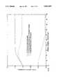
- FIG. 3illustrates that threshold voltage is dependent on the length of the p-channel transistor.
- the channel length usedmust be at least as great as that required to reach the relatively flat portion of the curve shown in FIG. 3. Since device size is limited by the channel length, reduction of the channel length is desired to obtain devices with smaller geometry. The "short channel” effect shown in FIG. 3 (i.e. variation in threshold voltage at short channel lengths) limits device geometry.
- additional n-dopingcould be added to raise the threshold voltage (V T ) of short channel transistors (i.e. 0.7 ⁇ m or less). However, such doping also affects longer channel transistors. Hence, the V T for these longer channels is higher than desirable because the higher V T will render low current drive and consequently the devices will be slower.
- Another object of the present inventionis to provide an improved method for formation of a p-channel semiconductor device which utilizes boron penetration to suppress the "short channel” effect and create a device whose threshold voltage is not a function of channel length.
- the preferred embodiment of the present inventionis a method for forming a set of p-channel devices by selectively allowing boron to penetrate into the channel region (ordinarily an undesirable phenomenon) between the source and drain regions, thereby creating channel length independent p-channel threshold voltage behavior.
- the effects of boron penetration and increased n-dopingare offset in longer channel transistors, and of increased n-doping in short channel transistors (where boron penetration has little effect), provide a device in which long channel and short channel transistors have approximately equal threshold voltages.
- FIG. 1illustrates a p-type MOS device
- FIG. 2(a)illustrates current flow from the source to the drain region of the type of device shown in FIG. 1;
- FIG. 2(b)illustrates current flow from the source to drain regions as a function of channel length
- FIG. 3shows dependence of threshold voltage on channel length in the type of device shown in FIG. 1;
- FIGS. 4(a) and (b)illustrate the effect of increased n-doping on threshold Voltage behavior
- FIG. 5shows the characteristics of p-channel threshold voltages when the effect of boron penetration is minimized
- FIG. 6illustrates the effect of various degrees of boron penetration on threshold voltage and its impact on different channel length transistors
- FIGS. 7(a) and (b)show boron diffusion in polysilicon pads of different length
- FIG. 7(c)shows boron concentration as a function of position along the channel length
- FIG. 7(d)shows the effect of boron penetration on threshold voltage in a long channel device
- FIG. 8shows the effect of boron penetration on threshold voltage
- FIG. 9shows the resultant channel length independent p-channel threshold voltage behavior when the boron penetration effect of FIG. 8 is combined with the short channel effect of FIG. 4(b);
- FIGS. 10(A)-10(H)shows a process sequence in accordance with the present invention.
- threshold voltageWith reference to FIG. 3, fall off of threshold voltage with channel length is shown.
- the example in this graphshows a threshold voltage of around -1.0 V, but it should be understood that threshold voltages vary with different technologies.
- the present inventionis not limited to a particular threshold voltage.
- Line widths in semiconductor devices manufactured with the current state of the arttypically vary from 0.8 ⁇ m to 20 ⁇ m within a single chip. "Short channel effect" limits use of smaller line widths.
- the present inventionuses increased n-doping and boron penetration to obtain threshold voltage behavior which is relatively constant from channel lengths of 0.1 ⁇ m to 20 ⁇ m, so that the threshold behavior in the resultant chip is relatively constant regardless of channel length.
- FIGS. 4(a) and (b)illustrate the shift in threshold voltage behavior that can be achieved by increasing the dopant concentration of the n-doped region of a device.
- This methodwill increase the threshold voltage of the shorter channel and longer channel transistors simultaneously. Note that the threshold voltage is increased to a greater absolute value of V t by increased n-doping.
- the increase in threshold voltage as shown in FIGS. 4(a) and (b)can be achieved with techniques and process conditions that are well known in the art, but such increases are generally not desirable since the long channel devices will then have too high threshold voltages (causing current drive to be small).
- the present processcan be easily adjusted with techniques known in the art to achieve the desired level of n-doping, which will vary with the technology used.
- the level of n-doping used in current technologyis in the range of 10 16 cm -3 to 10 18 cm -3 , and preferably in the range of 10 17 cm -3 to 10 18 cm -3 , but the present technique is general and can be used with different levels of n-doping.
- tungsten silicideis often use as a low-resistance gate material on top of polysilicon gate 22.
- Tungsten silicide formationusually involves a reduction process from a fluorine precursor species.
- the p-doped source and drain regionsare formed by implanting with BF 2 + ions. Both of these processes introduce fluorine atoms into polysilicon gate 22. These fluorine atoms enhance the diffusion of boron through the polysilicon layer, and aid diffusion of boron through the gate oxide (i.e., the silicon dioxide 20 below polysilicon 22) into channel region 18.
- special careis required to eliminate boron penetration into the channel region. If care is not taken, threshold voltage instability as a function of channel length is observed.
- FIG. 5shows the characteristics of p-channel threshold voltages as a function of channel length with the effect of boron penetration is minimized through control of process conditions.
- FIG. 6is an example of the typical characteristics of p-channel device threshold voltages as a function of channel length, with varying degrees of boron penetration.
- Thermal cycle and the p-implant dosageare the main driving forces for boron diffusion through the polysilicon into the gate oxide.
- the thickness of the polysilicon gateplays a major role in determining the onset of the threshold voltage roll-off due to boron penetration.
- FIGS. 5 and 6show that the effect of threshold voltage instability due to boron penetration impacts devices with long channel lengths, rather than devices with short channel lengths.
- the threshold voltage roll-off on the left of the channel length scale in both FIGS. 5 and 6is due to the "short channel effect" (drain-induced barrier-lowering effect).
- the threshold voltage in the short channel regimeis not affected at all by boron penetration.
- FIGS. 7(a) and 7(b)show the diffusion of boron atoms from a polysilicon gate area such as 22 in FIG. 1.
- FIG. 7(a)illustrates a short channel device.
- boronwill diffuse out of the polysilicon because it has less distance to go to the walls of the polysilicon than to the oxide and n-doped layer. Boron atoms diffuse into the ambient from the site of the polysilicon gate edge before they make it down to the polysilicon/oxide (20/22) interface.
- a longer channel devicesuch as shown in FIG.
- FIG. 7(b)boron will diffuse through polysilicon to the n-doped layer because the length out of the polysilicon layer is greater than the distance to the n-doped layer.
- FIG. 7(c)shows, the distribution of boron will thus tend to be greater in the center of the polysilicon pad.
- the boron penetrationwill have greater effect as channel length increases.
- FIG. 7(d)shows that the effect on threshold voltage for a long channel device with boron penetration, shifting the threshold voltage curve to the left.
- FIG. 8illustrates the change in threshold voltage due to boron penetration, i.e., boron penetration decreases the absolute value of the threshold voltage.
- FIG. 8illustrates that combination of the effects shown in FIGS. 4(b) (upper curve in FIG. 9) and 8 (lower curve in FIG. 9) creates a device which has the performance of the middle curve of FIG. 9, i.e., p-channel threshold voltage behavior that is relatively constant from short through long channels (preferably varying by less than 0.3 V, and more preferably by 0.1 V or less).
- FIG. 10illustrates a method in accordance with the present invention for constructing a set of devices in a chip (typically transistors devices) with different channel lengths but relatively constant threshold voltage.
- FIG. 10(a)shows an n-doped silicon substrate 12 on which gate oxide 20 is grown. Typical gate oxide thickness range is between 80-150 Angstroms. Note that the n-doped silicon substrate could also be an n-well or n-tub inside a p-substrate.
- polysilicon 22is deposited by CVD over the oxide. Polysilicon thickness is tailored, depending on the overall amount of the thermal budget in the process, in order to obtain the maximum benefit of this invention. In the preferred embodiment, polysilicon thickness around 1000-1500 Angstroms is used.
- Tungsten silicide 24 with thickness of 1500-2000 Angstromsis also deposited to reduce the resistance of the polysilicon gate.
- FIG. 10(c)shows patterned photoresist 26 over these layers.
- the tungsten silicide 24, polysilicon 22 and oxide 20are etched, removing the tungsten silicide, polysilicon and oxide which are not protected by photoresist 26.
- a pad consisting of tungsten silicide and polysiliconremains over the gate oxide.
- BF 2 + ion implantationtakes place, with dosage in the range of 5 ⁇ 10 15 cm -2 to 7 ⁇ 10 15 cm -2 and implant energy of 60 KeV, which creates p-doped layers 14 on both sides of the gate oxide.
- Boon implantation dosagewill vary with the process used. With present processes, implantation dosage in the range of 10 15 cm -2 to 10 16 cm -2 is preferred.
- the tungsten silicide 24 and polysilicon layers 22 overlying the gate oxide 20also receive boron ions.
- the boron in a "short channel"in this case 0.7 ⁇ m or below
- polysilicon layer overlying the gate area for the most partis diffused out of the polysilicon and into the ambient.
- boronis diffused into the underlying n-type silicon layer, creating greater boron penetration effects in longer channel devices.
Landscapes
- Engineering & Computer Science (AREA)
- Physics & Mathematics (AREA)
- Condensed Matter Physics & Semiconductors (AREA)
- General Physics & Mathematics (AREA)
- Manufacturing & Machinery (AREA)
- Computer Hardware Design (AREA)
- Microelectronics & Electronic Packaging (AREA)
- Power Engineering (AREA)
- Chemical & Material Sciences (AREA)
- Chemical Kinetics & Catalysis (AREA)
- Insulated Gate Type Field-Effect Transistor (AREA)
- Metal-Oxide And Bipolar Metal-Oxide Semiconductor Integrated Circuits (AREA)
Abstract
Description
1. Field of the Invention
This invention relates generally to a method for forming a p-channel semiconductor device in which the threshold voltage is not a function of channel length, and more particularly to a method which utilizes boron penetration to suppress short channel effect.
2. Brief Description of the Prior Art
Metal oxide semiconductor (MOS) devices are well known in the prior art. FIG. 1 illustrates a p-type MOS device. Thedevice 10 includes an n-dopedsilicon layer 12, and p-dopedsilicon source 14 and drain 16 regions. Note that the n-doped silicon substrate could also be an n-well or n-tub inside a p-substrate. The separation between the drain and source regions is typically around 0.8 μm in the present state of the art. A layer ofsilicon dioxide 20 overlies these areas, and apolysilicon layer 22 is placed over the area ("channel") between source and drain regions, defining a "gate" region. Normally with OV or positive voltage on the gate, no p-type conduction is formed between the source and drain regions, thus no current can flow between them. When a negative bias is applied across the gate region, the n-type region inchannel 18 will gradually be depleted away until it becomes "inverted", i.e., a p-type conduction region is formed out of the n-type region that connects source anddrain regions channel region 18. FIG. 2(a) illustrates that for a fixed channel length (typically on the order of 0.8 μm), the current from the source to the drain region will approach a constant value known as saturation current when the gate voltage is increasing in the negative direction and reaches the threshold level (Vt) where current flow reaches a level suitable for reliable operation of the device.
FIG. 2(b) illustrates current flow from source to drain regions with different channel lengths. Note that at shorter channel lengths, current flows even at positive voltages, and reliable device performance (which requires that the device be distinctly "on" or "off") cannot be obtained.
FIG. 3 illustrates that threshold voltage is dependent on the length of the p-channel transistor. In order to obtain satisfactory performance, the channel length used must be at least as great as that required to reach the relatively flat portion of the curve shown in FIG. 3. Since device size is limited by the channel length, reduction of the channel length is desired to obtain devices with smaller geometry. The "short channel" effect shown in FIG. 3 (i.e. variation in threshold voltage at short channel lengths) limits device geometry. Typically, additional n-doping could be added to raise the threshold voltage (VT) of short channel transistors (i.e. 0.7 μm or less). However, such doping also affects longer channel transistors. Hence, the VT for these longer channels is higher than desirable because the higher VT will render low current drive and consequently the devices will be slower.
It is the primary object of the present invention to provide a p-channel device in which the "short channel" effect is suppressed by a combination of boron penetration and increased n-doping.
Another object of the present invention is to provide an improved method for formation of a p-channel semiconductor device which utilizes boron penetration to suppress the "short channel" effect and create a device whose threshold voltage is not a function of channel length.
Briefly, the preferred embodiment of the present invention is a method for forming a set of p-channel devices by selectively allowing boron to penetrate into the channel region (ordinarily an undesirable phenomenon) between the source and drain regions, thereby creating channel length independent p-channel threshold voltage behavior. The effects of boron penetration and increased n-doping are offset in longer channel transistors, and of increased n-doping in short channel transistors (where boron penetration has little effect), provide a device in which long channel and short channel transistors have approximately equal threshold voltages.
FIG. 1 illustrates a p-type MOS device;
FIG. 2(a) illustrates current flow from the source to the drain region of the type of device shown in FIG. 1;
FIG. 2(b) illustrates current flow from the source to drain regions as a function of channel length;
FIG. 3 shows dependence of threshold voltage on channel length in the type of device shown in FIG. 1;
FIGS. 4(a) and (b) illustrate the effect of increased n-doping on threshold Voltage behavior;
FIG. 5 shows the characteristics of p-channel threshold voltages when the effect of boron penetration is minimized;
FIG. 6 illustrates the effect of various degrees of boron penetration on threshold voltage and its impact on different channel length transistors;
FIGS. 7(a) and (b) show boron diffusion in polysilicon pads of different length;
FIG. 7(c) shows boron concentration as a function of position along the channel length;
FIG. 7(d) shows the effect of boron penetration on threshold voltage in a long channel device;
FIG. 8 shows the effect of boron penetration on threshold voltage;
FIG. 9 shows the resultant channel length independent p-channel threshold voltage behavior when the boron penetration effect of FIG. 8 is combined with the short channel effect of FIG. 4(b); and
FIGS. 10(A)-10(H) shows a process sequence in accordance with the present invention.
With reference to FIG. 3, fall off of threshold voltage with channel length is shown. The example in this graph shows a threshold voltage of around -1.0 V, but it should be understood that threshold voltages vary with different technologies. The present invention is not limited to a particular threshold voltage. Line widths in semiconductor devices manufactured with the current state of the art typically vary from 0.8 μm to 20 μm within a single chip. "Short channel effect" limits use of smaller line widths. In order to obtain stable performance, it is desirable to have threshold voltage remain relatively constant regardless of channel length (around -1.0 V in the example in FIG. 3). This ideal performance is shown by the horizontal dashed line in FIG. 3. The present invention uses increased n-doping and boron penetration to obtain threshold voltage behavior which is relatively constant from channel lengths of 0.1 μm to 20 μm, so that the threshold behavior in the resultant chip is relatively constant regardless of channel length.
FIGS. 4(a) and (b) illustrate the shift in threshold voltage behavior that can be achieved by increasing the dopant concentration of the n-doped region of a device. This method will increase the threshold voltage of the shorter channel and longer channel transistors simultaneously. Note that the threshold voltage is increased to a greater absolute value of Vt by increased n-doping. The increase in threshold voltage as shown in FIGS. 4(a) and (b) can be achieved with techniques and process conditions that are well known in the art, but such increases are generally not desirable since the long channel devices will then have too high threshold voltages (causing current drive to be small). The present process can be easily adjusted with techniques known in the art to achieve the desired level of n-doping, which will vary with the technology used. In general, the level of n-doping used in current technology is in the range of 1016 cm-3 to 1018 cm-3, and preferably in the range of 1017 cm-3 to 1018 cm-3, but the present technique is general and can be used with different levels of n-doping.
Referring again to FIG. 1, in a conventional CMOS process, tungsten silicide is often use as a low-resistance gate material on top ofpolysilicon gate 22. Tungsten silicide formation usually involves a reduction process from a fluorine precursor species. In addition, the p-doped source and drain regions are formed by implanting with BF2 + ions. Both of these processes introduce fluorine atoms intopolysilicon gate 22. These fluorine atoms enhance the diffusion of boron through the polysilicon layer, and aid diffusion of boron through the gate oxide (i.e., thesilicon dioxide 20 below polysilicon 22) intochannel region 18. In the prior art, special care is required to eliminate boron penetration into the channel region. If care is not taken, threshold voltage instability as a function of channel length is observed.
FIG. 5 shows the characteristics of p-channel threshold voltages as a function of channel length with the effect of boron penetration is minimized through control of process conditions. FIG. 6 is an example of the typical characteristics of p-channel device threshold voltages as a function of channel length, with varying degrees of boron penetration. Thermal cycle and the p-implant dosage are the main driving forces for boron diffusion through the polysilicon into the gate oxide. In general, the thickness of the polysilicon gate plays a major role in determining the onset of the threshold voltage roll-off due to boron penetration.
FIGS. 5 and 6 show that the effect of threshold voltage instability due to boron penetration impacts devices with long channel lengths, rather than devices with short channel lengths. The threshold voltage roll-off on the left of the channel length scale in both FIGS. 5 and 6 is due to the "short channel effect" (drain-induced barrier-lowering effect). The threshold voltage in the short channel regime is not affected at all by boron penetration.
The reason that boron penetration does not affect threshold voltages for short channel lengths is illustrated in FIGS. 7(a) and 7(b), which show the diffusion of boron atoms from a polysilicon gate area such as 22 in FIG. 1. FIG. 7(a) illustrates a short channel device. When the polysilicon pad is short, boron will diffuse out of the polysilicon because it has less distance to go to the walls of the polysilicon than to the oxide and n-doped layer. Boron atoms diffuse into the ambient from the site of the polysilicon gate edge before they make it down to the polysilicon/oxide (20/22) interface. However, in a longer channel device such as shown in FIG. 7(b), boron will diffuse through polysilicon to the n-doped layer because the length out of the polysilicon layer is greater than the distance to the n-doped layer. As FIG. 7(c) shows, the distribution of boron will thus tend to be greater in the center of the polysilicon pad. Hence, the boron penetration will have greater effect as channel length increases. This schematic illustration correlates well with the effect shown in FIG. 6. FIG. 7(d) shows that the effect on threshold voltage for a long channel device with boron penetration, shifting the threshold voltage curve to the left. FIG. 8 illustrates the change in threshold voltage due to boron penetration, i.e., boron penetration decreases the absolute value of the threshold voltage.
The phenomena illustrated in FIG. 8 (fall off of threshold voltage with increasing channel length due to boron penetration) and FIG. 4 (the ability to tailor threshold voltage roll-off by tailoring polysilicon gate thickness with control of doping and phosphorus concentration and polysilicon) may be combined. The combination of the n-doping effect threshold voltage increase shown in FIG. 4 and the boron penetration effect shown in FIG. 8 yield a process where the short channel effect and the boron penetration effect (both of which are considered problems to be overcome in manufacturing) are used together to create threshold behavior that is relatively independent of channel length. FIG. 9 illustrates that combination of the effects shown in FIGS. 4(b) (upper curve in FIG. 9) and 8 (lower curve in FIG. 9) creates a device which has the performance of the middle curve of FIG. 9, i.e., p-channel threshold voltage behavior that is relatively constant from short through long channels (preferably varying by less than 0.3 V, and more preferably by 0.1 V or less).
FIG. 10 illustrates a method in accordance with the present invention for constructing a set of devices in a chip (typically transistors devices) with different channel lengths but relatively constant threshold voltage. FIG. 10(a) shows an n-dopedsilicon substrate 12 on whichgate oxide 20 is grown. Typical gate oxide thickness range is between 80-150 Angstroms. Note that the n-doped silicon substrate could also be an n-well or n-tub inside a p-substrate. In FIG. 10(b),polysilicon 22 is deposited by CVD over the oxide. Polysilicon thickness is tailored, depending on the overall amount of the thermal budget in the process, in order to obtain the maximum benefit of this invention. In the preferred embodiment, polysilicon thickness around 1000-1500 Angstroms is used.Tungsten silicide 24 with thickness of 1500-2000 Angstroms is also deposited to reduce the resistance of the polysilicon gate. FIG. 10(c) shows patternedphotoresist 26 over these layers. In FIG. 10(d), thetungsten silicide 24,polysilicon 22 andoxide 20 are etched, removing the tungsten silicide, polysilicon and oxide which are not protected byphotoresist 26. After stripping of the photoresist as shown in FIG. 10(e), a pad consisting of tungsten silicide and polysilicon remains over the gate oxide. In FIG. 10(f), BF2 + ion implantation takes place, with dosage in the range of 5×1015 cm-2 to 7×1015 cm-2 and implant energy of 60 KeV, which creates p-dopedlayers 14 on both sides of the gate oxide. (Boron implantation dosage will vary with the process used. With present processes, implantation dosage in the range of 1015 cm-2 to 1016 cm-2 is preferred.) Thetungsten silicide 24 andpolysilicon layers 22 overlying thegate oxide 20 also receive boron ions. In FIG. 10(g), the boron in a "short channel" (in this case 0.7 μm or below) polysilicon layer overlying the gate area for the most part is diffused out of the polysilicon and into the ambient. However, with long channel lengths as shown in FIG. 10(h), boron is diffused into the underlying n-type silicon layer, creating greater boron penetration effects in longer channel devices.
Although the present invention has been described above in terms of a specific embodiment, it is anticipated that alterations and modifications thereof will, no doubt, become apparent to those skilled in the art. It is, therefore, intended that the following claims be interpreted as covering all such alterations and modifications as fall within the true spirit and scope of the invention.
Claims (6)
1. A method for controlling the threshold voltage for a set of p-channel devices formed on a semiconductor substrate, in which the devices have different channel lengths, comprising the steps of:
(a) providing an n-doped semiconductor substrate, wherein the n-doping is sufficient to control the threshold voltage within 0.3 volts for p-channel devices with channel lengths of less than 0.6 μm;
(b) forming a set of p-channel devices with gate regions having different channel lengths, said lengths varying from less than 0.6 μm to at least 3 μm; and
(c) causing boron to penetrate into the gate regions of the p-channel devices, whereby the absolute values of the threshold voltage for the devices decreases with increasing channel length, thereby offsetting the effect of n-doping of the substrate for long channel lengths and creating a set of p-channel devices having said controlled threshold voltage behavior for channel lengths from less than 0.6 μm to channel lengths of greater than 3 μm, wherein the threshold voltage is defined as 85% of the saturation voltage.
2. The method of claim 1, wherein the threshold voltage is controlled within 0.3 volts for devices having channel lengths from less than 0.3 μm to greater than 10 μm.
3. The method of claim 1, wherein the n-doping level is in the range of 1017 cm-3 to 1018 cm-3.
4. The method of claim 3, wherein the boron implantation dosage is in the range of 1015 cm-2 to 1016 cm-2.
5. The method of claim 2, wherein the n-doping level is in the range of 1017 cm-3 to 1018 cm-3.
6. The method of claim 5, wherein the boron implantation dosage is in the range of 1015 cm-2 to 1016 cm-2.
Priority Applications (1)
| Application Number | Priority Date | Filing Date | Title |
|---|---|---|---|
| US08/423,109US5661059A (en) | 1995-04-18 | 1995-04-18 | Boron penetration to suppress short channel effect in P-channel device |
Applications Claiming Priority (1)
| Application Number | Priority Date | Filing Date | Title |
|---|---|---|---|
| US08/423,109US5661059A (en) | 1995-04-18 | 1995-04-18 | Boron penetration to suppress short channel effect in P-channel device |
Publications (1)
| Publication Number | Publication Date |
|---|---|
| US5661059Atrue US5661059A (en) | 1997-08-26 |
Family
ID=23677713
Family Applications (1)
| Application Number | Title | Priority Date | Filing Date |
|---|---|---|---|
| US08/423,109Expired - LifetimeUS5661059A (en) | 1995-04-18 | 1995-04-18 | Boron penetration to suppress short channel effect in P-channel device |
Country Status (1)
| Country | Link |
|---|---|
| US (1) | US5661059A (en) |
Cited By (19)
| Publication number | Priority date | Publication date | Assignee | Title |
|---|---|---|---|---|
| US6118148A (en)* | 1996-11-04 | 2000-09-12 | Semiconductor Energy Laboratory Co., Ltd. | Semiconductor device and manufacturing method thereof |
| US6198141B1 (en) | 1996-08-13 | 2001-03-06 | Semiconductor Energy Laboratory Co., Ltd. | Insulated gate semiconductor device and method of manufacturing the same |
| GB2355851A (en)* | 1999-06-24 | 2001-05-02 | Lucent Technologies Inc | Short gate/channel MOSFET |
| US6232642B1 (en) | 1997-06-26 | 2001-05-15 | Semiconductor Energy Laboratory Co., Ltd. | Semiconductor device having impurity region locally at an end of channel formation region |
| US6271563B1 (en) | 1998-07-27 | 2001-08-07 | Advanced Micro Devices, Inc. | MOS transistor with high-K spacer designed for ultra-large-scale integration |
| US6590230B1 (en) | 1996-10-15 | 2003-07-08 | Semiconductor Energy Laboratory Co., Ltd. | Semiconductor device and manufacturing method thereof |
| US20030216015A1 (en)* | 2002-05-17 | 2003-11-20 | Mitsubishi Denki Kabushiki Kaisha | Method of manufacturing semiconductor device |
| US6653687B1 (en) | 1996-08-13 | 2003-11-25 | Semiconductor Energy Laboratory Co., Ltd. | Insulated gate semiconductor device |
| US6686623B2 (en) | 1997-11-18 | 2004-02-03 | Semiconductor Energy Laboratory Co., Ltd. | Nonvolatile memory and electronic apparatus |
| US6740912B1 (en) | 1999-06-24 | 2004-05-25 | Agere Systems Inc. | Semiconductor device free of LLD regions |
| US20050181565A1 (en)* | 2003-10-20 | 2005-08-18 | Ethan Williford | Threshold voltage adjustment for long channel transistors |
| US20050189572A1 (en)* | 1998-02-05 | 2005-09-01 | Semiconductor Energy Laboratory Co., Ltd., A Japan Corporation | Semiconductor device and method of manufacturing the same |
| US20070148890A1 (en)* | 2005-12-27 | 2007-06-28 | Enicks Darwin G | Oxygen enhanced metastable silicon germanium film layer |
| US20070262295A1 (en)* | 2006-05-11 | 2007-11-15 | Atmel Corporation | A method for manipulation of oxygen within semiconductor materials |
| US7339235B1 (en) | 1996-09-18 | 2008-03-04 | Semiconductor Energy Laboratory Co., Ltd. | Semiconductor device having SOI structure and manufacturing method thereof |
| US8173526B2 (en) | 2006-10-31 | 2012-05-08 | Atmel Corporation | Method for providing a nanoscale, high electron mobility transistor (HEMT) on insulator |
| US8530934B2 (en) | 2005-11-07 | 2013-09-10 | Atmel Corporation | Integrated circuit structures containing a strain-compensated compound semiconductor layer and methods and systems related thereto |
| US20160125805A1 (en)* | 2006-08-18 | 2016-05-05 | Sony Corporation | Image display device and electronic appliance |
| CN113611609A (en)* | 2021-07-29 | 2021-11-05 | 上海华虹宏力半导体制造有限公司 | Manufacturing method of MOS device |
Citations (5)
| Publication number | Priority date | Publication date | Assignee | Title |
|---|---|---|---|---|
| US4587709A (en)* | 1983-06-06 | 1986-05-13 | International Business Machines Corporation | Method of making short channel IGFET |
| US4701423A (en)* | 1985-12-20 | 1987-10-20 | Ncr Corporation | Totally self-aligned CMOS process |
| US5091324A (en)* | 1990-08-10 | 1992-02-25 | Advanced Micro Devices, Inc. | Process for producing optimum intrinsic, long channel, and short channel mos devices in vlsi structures |
| US5407849A (en)* | 1992-06-23 | 1995-04-18 | Imp, Inc. | CMOS process and circuit including zero threshold transistors |
| US5548143A (en)* | 1993-04-29 | 1996-08-20 | Samsung Electronics Co., Ltd. | Metal oxide semiconductor transistor and a method for manufacturing the same |
- 1995
- 1995-04-18USUS08/423,109patent/US5661059A/ennot_activeExpired - Lifetime
Patent Citations (5)
| Publication number | Priority date | Publication date | Assignee | Title |
|---|---|---|---|---|
| US4587709A (en)* | 1983-06-06 | 1986-05-13 | International Business Machines Corporation | Method of making short channel IGFET |
| US4701423A (en)* | 1985-12-20 | 1987-10-20 | Ncr Corporation | Totally self-aligned CMOS process |
| US5091324A (en)* | 1990-08-10 | 1992-02-25 | Advanced Micro Devices, Inc. | Process for producing optimum intrinsic, long channel, and short channel mos devices in vlsi structures |
| US5407849A (en)* | 1992-06-23 | 1995-04-18 | Imp, Inc. | CMOS process and circuit including zero threshold transistors |
| US5548143A (en)* | 1993-04-29 | 1996-08-20 | Samsung Electronics Co., Ltd. | Metal oxide semiconductor transistor and a method for manufacturing the same |
Cited By (42)
| Publication number | Priority date | Publication date | Assignee | Title |
|---|---|---|---|---|
| US6653687B1 (en) | 1996-08-13 | 2003-11-25 | Semiconductor Energy Laboratory Co., Ltd. | Insulated gate semiconductor device |
| US6198141B1 (en) | 1996-08-13 | 2001-03-06 | Semiconductor Energy Laboratory Co., Ltd. | Insulated gate semiconductor device and method of manufacturing the same |
| US6867085B2 (en) | 1996-08-13 | 2005-03-15 | Semiconductor Energy Laboratory Co., Ltd. | Insulated gate semiconductor device and method of manufacturing the same |
| US7339235B1 (en) | 1996-09-18 | 2008-03-04 | Semiconductor Energy Laboratory Co., Ltd. | Semiconductor device having SOI structure and manufacturing method thereof |
| US6590230B1 (en) | 1996-10-15 | 2003-07-08 | Semiconductor Energy Laboratory Co., Ltd. | Semiconductor device and manufacturing method thereof |
| US6118148A (en)* | 1996-11-04 | 2000-09-12 | Semiconductor Energy Laboratory Co., Ltd. | Semiconductor device and manufacturing method thereof |
| US6251733B1 (en)* | 1996-11-04 | 2001-06-26 | Semiconductor Energy Laboratory Co., Ltd. | Semiconductor device and manufacturing method thereof |
| US6690075B2 (en)* | 1996-11-04 | 2004-02-10 | Semiconductor Energy Laboratory Co., Ltd. | Semiconductor device with channel having plural impurity regions |
| US6232642B1 (en) | 1997-06-26 | 2001-05-15 | Semiconductor Energy Laboratory Co., Ltd. | Semiconductor device having impurity region locally at an end of channel formation region |
| US8222696B2 (en) | 1997-11-18 | 2012-07-17 | Semiconductor Energy Laboratory Co., Ltd. | Semiconductor device having buried oxide film |
| US20040104424A1 (en)* | 1997-11-18 | 2004-06-03 | Semiconductor Energy Laboratory Co., Ltd. | Nonvolatile memory and electronic apparatus |
| US6686623B2 (en) | 1997-11-18 | 2004-02-03 | Semiconductor Energy Laboratory Co., Ltd. | Nonvolatile memory and electronic apparatus |
| US8482069B2 (en) | 1997-11-18 | 2013-07-09 | Semiconductor Energy Laboratory Co., Ltd. | Nonvolatile memory and electronic apparatus |
| US7535053B2 (en) | 1997-11-18 | 2009-05-19 | Semiconductor Energy Laboratory Co., Ltd. | Nonvolatile memory and electronic apparatus |
| US20050189572A1 (en)* | 1998-02-05 | 2005-09-01 | Semiconductor Energy Laboratory Co., Ltd., A Japan Corporation | Semiconductor device and method of manufacturing the same |
| US7671425B2 (en) | 1998-02-05 | 2010-03-02 | Semiconductor Energy Laboratory Co., Ltd. | Semiconductor device and method of manufacturing the same |
| US6271563B1 (en) | 1998-07-27 | 2001-08-07 | Advanced Micro Devices, Inc. | MOS transistor with high-K spacer designed for ultra-large-scale integration |
| US6740912B1 (en) | 1999-06-24 | 2004-05-25 | Agere Systems Inc. | Semiconductor device free of LLD regions |
| GB2355851B (en)* | 1999-06-24 | 2003-11-19 | Lucent Technologies Inc | MOS Transistor |
| GB2355851A (en)* | 1999-06-24 | 2001-05-02 | Lucent Technologies Inc | Short gate/channel MOSFET |
| US20030216015A1 (en)* | 2002-05-17 | 2003-11-20 | Mitsubishi Denki Kabushiki Kaisha | Method of manufacturing semiconductor device |
| US6841459B2 (en)* | 2002-05-17 | 2005-01-11 | Renesas Technology Corp. | Method of manufacturing semiconductor device |
| US9111958B2 (en) | 2003-10-20 | 2015-08-18 | Micron Technology, Inc. | Threshold voltage adjustment of a transistor |
| US7422948B2 (en) | 2003-10-20 | 2008-09-09 | Micron Technology, Inc. | Threshold voltage adjustment for long channel transistors |
| US10032903B2 (en) | 2003-10-20 | 2018-07-24 | Micron Technology, Inc. | Threshold voltage adjustment of a transistor |
| US20050181565A1 (en)* | 2003-10-20 | 2005-08-18 | Ethan Williford | Threshold voltage adjustment for long channel transistors |
| US7968411B2 (en) | 2003-10-20 | 2011-06-28 | Micron Technology, Inc. | Threshold voltage adjustment for long-channel transistors |
| US20110233671A1 (en)* | 2003-10-20 | 2011-09-29 | Micron Technology, Inc. | Threshold voltage adjustment of a transistor |
| US7274076B2 (en) | 2003-10-20 | 2007-09-25 | Micron Technology, Inc. | Threshold voltage adjustment for long channel transistors |
| US20080054375A1 (en)* | 2003-10-20 | 2008-03-06 | Micron Technology, Inc. | Threshold voltage adjustment for long-channel transistors |
| US8530934B2 (en) | 2005-11-07 | 2013-09-10 | Atmel Corporation | Integrated circuit structures containing a strain-compensated compound semiconductor layer and methods and systems related thereto |
| US9012308B2 (en) | 2005-11-07 | 2015-04-21 | Atmel Corporation | Integrated circuit structures containing a strain-compensated compound semiconductor layer and methods and systems related thereto |
| US20070148890A1 (en)* | 2005-12-27 | 2007-06-28 | Enicks Darwin G | Oxygen enhanced metastable silicon germanium film layer |
| US20070262295A1 (en)* | 2006-05-11 | 2007-11-15 | Atmel Corporation | A method for manipulation of oxygen within semiconductor materials |
| WO2007133949A1 (en)* | 2006-05-11 | 2007-11-22 | Atmel Corporation | A method for manipulation of oxygen within semiconductor materials |
| US20160125805A1 (en)* | 2006-08-18 | 2016-05-05 | Sony Corporation | Image display device and electronic appliance |
| US9984621B2 (en)* | 2006-08-18 | 2018-05-29 | Sony Corporation | Image display device having a drive transistor with a channel length longer than a channel length of individual switching transistors |
| US10229638B2 (en) | 2006-08-18 | 2019-03-12 | Sony Corporation | Image display device having a drive transistor with a channel length longer than a channel length of individual switching transistors |
| US10706777B2 (en) | 2006-08-18 | 2020-07-07 | Sony Corporation | Image display device having a drive transistor with a channel length longer than a channel length of individual switching transistors |
| US11114029B2 (en) | 2006-08-18 | 2021-09-07 | Sony Corporation | Image display device having a drive transistor with a channel length longer than a channel length of individual switching transistors |
| US8173526B2 (en) | 2006-10-31 | 2012-05-08 | Atmel Corporation | Method for providing a nanoscale, high electron mobility transistor (HEMT) on insulator |
| CN113611609A (en)* | 2021-07-29 | 2021-11-05 | 上海华虹宏力半导体制造有限公司 | Manufacturing method of MOS device |
Similar Documents
| Publication | Publication Date | Title |
|---|---|---|
| US5661059A (en) | Boron penetration to suppress short channel effect in P-channel device | |
| US5422506A (en) | Field effect transistor structure heavily doped source/drain regions and lightly doped source/drain regions | |
| US5465000A (en) | Threshold adjustment in vertical DMOS devices | |
| US6503805B2 (en) | Channel implant through gate polysilicon | |
| US7382024B2 (en) | Low threshold voltage PMOS apparatus and method of fabricating the same | |
| US7326975B2 (en) | Buried channel type transistor having a trench gate and method of manufacturing the same | |
| US7064399B2 (en) | Advanced CMOS using super steep retrograde wells | |
| US5371024A (en) | Semiconductor device and process for manufacturing the same | |
| JP4540438B2 (en) | Semiconductor device and manufacturing method thereof | |
| US5923985A (en) | MOS field effect transistor and its manufacturing method | |
| US6049113A (en) | Semiconductor device and semiconductor device manufacturing method | |
| USRE32800E (en) | Method of making mosfet by multiple implantations followed by a diffusion step | |
| JP4145364B2 (en) | DMOS structure and manufacturing method thereof | |
| JPH08250730A (en) | Method for manufacturing integrated circuit and method for reducing diffusion of p-type dopant, and integrated circuit | |
| US20030011009A1 (en) | Grooved channel schottky mosfet | |
| US10217838B2 (en) | Semiconductor structure with multiple transistors having various threshold voltages | |
| US7105413B2 (en) | Methods for forming super-steep diffusion region profiles in MOS devices and resulting semiconductor topographies | |
| US9362399B2 (en) | Well implant through dummy gate oxide in gate-last process | |
| US20040014303A1 (en) | Method of ion implantation for achieving desired dopant concentration | |
| US4987088A (en) | Fabrication of CMOS devices with reduced gate length | |
| US6407428B1 (en) | Field effect transistor with a buried and confined metal plate to control short channel effects | |
| US6882013B2 (en) | Transistor with reduced short channel effects and method | |
| US20030062572A1 (en) | Transistor with bottomwall/sidewall junction capacitance reduction region and method | |
| US7101746B2 (en) | Method to lower work function of gate electrode through Ge implantation | |
| KR100673101B1 (en) | BC PMOSOSFET and its manufacturing method |
Legal Events
| Date | Code | Title | Description |
|---|---|---|---|
| AS | Assignment | Owner name:ADVANCED MICRO DEVICES,INC., CALIFORNIA Free format text:ASSIGNMENT OF ASSIGNORS INTEREST;ASSIGNORS:LIU, DAVID;FANG, HAO;REEL/FRAME:007459/0099 Effective date:19950407 | |
| STCF | Information on status: patent grant | Free format text:PATENTED CASE | |
| FPAY | Fee payment | Year of fee payment:4 | |
| FPAY | Fee payment | Year of fee payment:8 | |
| FPAY | Fee payment | Year of fee payment:12 | |
| AS | Assignment | Owner name:GLOBALFOUNDRIES INC., CAYMAN ISLANDS Free format text:AFFIRMATION OF PATENT ASSIGNMENT;ASSIGNOR:ADVANCED MICRO DEVICES, INC.;REEL/FRAME:023119/0083 Effective date:20090630 | |
| AS | Assignment | Owner name:GLOBALFOUNDRIES U.S. INC., NEW YORK Free format text:RELEASE BY SECURED PARTY;ASSIGNOR:WILMINGTON TRUST, NATIONAL ASSOCIATION;REEL/FRAME:056987/0001 Effective date:20201117 |