US5661042A - Process for electrically connecting electrical devices using a conductive anisotropic material - Google Patents
Process for electrically connecting electrical devices using a conductive anisotropic materialDownload PDFInfo
- Publication number
- US5661042A US5661042AUS08/520,118US52011895AUS5661042AUS 5661042 AUS5661042 AUS 5661042AUS 52011895 AUS52011895 AUS 52011895AUS 5661042 AUS5661042 AUS 5661042A
- Authority
- US
- United States
- Prior art keywords
- removable
- semiconductor wafer
- placing
- axis
- probe substrate
- Prior art date
- Legal status (The legal status is an assumption and is not a legal conclusion. Google has not performed a legal analysis and makes no representation as to the accuracy of the status listed.)
- Expired - Lifetime
Links
Images

Classifications
- H—ELECTRICITY
- H01—ELECTRIC ELEMENTS
- H01L—SEMICONDUCTOR DEVICES NOT COVERED BY CLASS H10
- H01L21/00—Processes or apparatus adapted for the manufacture or treatment of semiconductor or solid state devices or of parts thereof
- H01L21/67—Apparatus specially adapted for handling semiconductor or electric solid state devices during manufacture or treatment thereof; Apparatus specially adapted for handling wafers during manufacture or treatment of semiconductor or electric solid state devices or components ; Apparatus not specifically provided for elsewhere
- H01L21/683—Apparatus specially adapted for handling semiconductor or electric solid state devices during manufacture or treatment thereof; Apparatus specially adapted for handling wafers during manufacture or treatment of semiconductor or electric solid state devices or components ; Apparatus not specifically provided for elsewhere for supporting or gripping
- H01L21/6835—Apparatus specially adapted for handling semiconductor or electric solid state devices during manufacture or treatment thereof; Apparatus specially adapted for handling wafers during manufacture or treatment of semiconductor or electric solid state devices or components ; Apparatus not specifically provided for elsewhere for supporting or gripping using temporarily an auxiliary support
- G—PHYSICS
- G01—MEASURING; TESTING
- G01R—MEASURING ELECTRIC VARIABLES; MEASURING MAGNETIC VARIABLES
- G01R1/00—Details of instruments or arrangements of the types included in groups G01R5/00 - G01R13/00 and G01R31/00
- G01R1/02—General constructional details
- G01R1/06—Measuring leads; Measuring probes
- G01R1/067—Measuring probes
- G01R1/073—Multiple probes
- G—PHYSICS
- G01—MEASURING; TESTING
- G01R—MEASURING ELECTRIC VARIABLES; MEASURING MAGNETIC VARIABLES
- G01R31/00—Arrangements for testing electric properties; Arrangements for locating electric faults; Arrangements for electrical testing characterised by what is being tested not provided for elsewhere
- G01R31/28—Testing of electronic circuits, e.g. by signal tracer
- G01R31/2851—Testing of integrated circuits [IC]
- G01R31/2855—Environmental, reliability or burn-in testing
- G01R31/286—External aspects, e.g. related to chambers, contacting devices or handlers
- G01R31/2863—Contacting devices, e.g. sockets, burn-in boards or mounting fixtures
- H—ELECTRICITY
- H01—ELECTRIC ELEMENTS
- H01L—SEMICONDUCTOR DEVICES NOT COVERED BY CLASS H10
- H01L2224/00—Indexing scheme for arrangements for connecting or disconnecting semiconductor or solid-state bodies and methods related thereto as covered by H01L24/00
- H01L2224/01—Means for bonding being attached to, or being formed on, the surface to be connected, e.g. chip-to-package, die-attach, "first-level" interconnects; Manufacturing methods related thereto
- H01L2224/10—Bump connectors; Manufacturing methods related thereto
- H01L2224/15—Structure, shape, material or disposition of the bump connectors after the connecting process
- H01L2224/16—Structure, shape, material or disposition of the bump connectors after the connecting process of an individual bump connector
- H—ELECTRICITY
- H01—ELECTRIC ELEMENTS
- H01L—SEMICONDUCTOR DEVICES NOT COVERED BY CLASS H10
- H01L2924/00—Indexing scheme for arrangements or methods for connecting or disconnecting semiconductor or solid-state bodies as covered by H01L24/00
- H01L2924/01—Chemical elements
- H01L2924/01079—Gold [Au]
- H—ELECTRICITY
- H05—ELECTRIC TECHNIQUES NOT OTHERWISE PROVIDED FOR
- H05K—PRINTED CIRCUITS; CASINGS OR CONSTRUCTIONAL DETAILS OF ELECTRIC APPARATUS; MANUFACTURE OF ASSEMBLAGES OF ELECTRICAL COMPONENTS
- H05K3/00—Apparatus or processes for manufacturing printed circuits
- H05K3/30—Assembling printed circuits with electric components, e.g. with resistor
- H05K3/32—Assembling printed circuits with electric components, e.g. with resistor electrically connecting electric components or wires to printed circuits
- H05K3/321—Assembling printed circuits with electric components, e.g. with resistor electrically connecting electric components or wires to printed circuits by conductive adhesives
- H05K3/323—Assembling printed circuits with electric components, e.g. with resistor electrically connecting electric components or wires to printed circuits by conductive adhesives by applying an anisotropic conductive adhesive layer over an array of pads
Definitions
- This inventionrelates, in general, to electronic devices, and more particularly, to materials and methods for providing temporary electrical contact.
- ICintegrated circuit
- semiconductor manufacturersPrior to shipping integrated circuit (IC) devices, semiconductor manufacturers generally screen the IC devices to ensure their reliability. Often, a burn-in testing process is used whereby a device is operated at a predetermined temperature level (typically at a fixed temperature in a range from about 85° C. to about 150° C.) over a prolonged period. Power is applied to certain contacts on the device during the burn-in period and performance is measured by monitoring output signals from the device. The burn-in process serves to screen out those devices that are susceptible to premature failure from, for example, latent defects.
- a predetermined temperature leveltypically at a fixed temperature in a range from about 85° C. to about 150° C.
- WLBIwafer-level burn-in
- One problem associated with WLBIis the lack of cost effective and reliable suitable for temporarily contacting a wafer to be tested to a test or probe substrate.
- One prior art method for WLBIincludes using an anisotropically conductive rubber sheet sandwiched between a wafer to be tested and a probe substrate.
- anisotropically conductive rubber sheetsis the need to use a clamping device throughout the burn-in process to hold the wafer, the rubber sheet, and the probe substrate together to ensure good contact.
- Clamping devicesare bulky and require frequent adjustment to avoid damaging the semiconductor wafer and/or the probe substrate. Additionally, because of their size, the clamping devices add significant thermal resistance and thermal mass thereby increasing burn-in process time. Furthermore, the clamping devices are not portable making it difficult to transport and store them (i.e., they are heavy and take up substantial space).
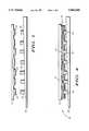
- FIG. 1illustrates an enlarged cross-sectional view of a semiconductor wafer and a probe substrate
- FIG. 2illustrates an enlarged cross-sectional view of a WLBI assembly at an intermediate step according to the present invention
- FIG. 3illustrates an enlarged cross-sectional view of a portion of the assembly shown in FIG. 2;
- FIG. 4illustrates a portion of an WLBI assembly at later step according to the present invention.
- the present inventioninvolves materials and methods that provide temporary electrical contact between electronic components.
- the inventionincludes a removable, non-permanent, or water-soluble Z-axis anisotropically conductive adhesive (ACA) material comprising water, a matrix resin, and a plurality of conductive spheres.
- ACAanisotropically conductive adhesive
- a methodfor providing electrical interconnection between electrical devices.
- the methodincludes depositing the removable Z-axis ACA material onto a first electrical device having a first conductive surface.
- the removable Z-axis ACA materialis then placed into contact with a second electrical device having a second conductive surface.
- the conductive spheres within the removable Z-axis ACA materialprovide an electrical interconnection between the first and second conductive surfaces when the first and second electrical devices are energized or biased during, for example, device testing. Once testing is complete, the first and second electrical devices may be separated by dissolving the removable Z-axis ACA material.
- the removable Z-axis ACA materialis used for wafer-level burn-in (WLBI).
- Z-axis ACA materialstypically are used as permanent adhesives to bond high-density printed-circuit assemblies including flexible interconnects and substrates.
- Permanent Z-axis ACA materialscomprise non-water soluble resin materials that can withstand harsh environments and are not easily removed.
- Z-axis ACA materialsconduct in one direction (e.g., in a vertical direction) and typically are used to provide a permanent conduction path between portions of an assembly.
- Permanent Z-axis ACA materialsare currently being developed by companies such as Poly-Flex Circuits Inc., 3M, Nippon Graphite, and AT&T Bell Labs for permanent printed-circuit assemblies. These permanent adhesives typically comprise proprietary mixtures of special resins and additives together with silver particles that provide the conduction path. Although these materials may be suitable as permanent adhesives, they are not suitable, for example, to temporarily bond a semiconductor substrate to a probe substrate for WLBI. This is because, among other things, they are difficult to remove from the substrates (i.e., strong solvents and extensive periods of time are necessary to breakdown or dissolve them). These strong solvents can cause irreversible damage to semiconductor devices and the probe substrates. These solvents also can damage the Conductive spheres Raking their re-use either impossible or limited.
- FIG. 1shows an enlarged cross-sectional view of a semiconductor wafer or substrate 11 in proximity to a probe substrate 12.
- Semiconductor wafer 11typically is referred to as a wafer-under-test (WUT) and includes wafer contact portions, bond pads, or bumps 13, which comprise a conductive material (e.g., a metal, a conductive polymer, or the like).
- Wafer contact portions 13provide contact to individual IC devices formed on semiconductor wafer 11.
- Probe substrate 12typically comprises a ceramic or printed circuit board material and has several metallized probing objects or bumps 14 for making contact to wafer contact portions 13. Methods for forming wafer contact portions 13 and probing objects 14 are well known in the art. Probe substrate 12 typically is coupled (e.g., via an edge card connector (not shown)) to a test device for forcing voltage or current to IC devices formed on semiconductor wafer 11 and measuring current or voltage from the IC devices. Such test devices are well known in the art.
- FIG. 1illustrates several problems that manufacturers face with WLBI. For example, contact between wafer contact portions 13 and probing objects 14 is difficult because their thicknesses typically are non-uniform. Also, one of or both of semiconductor wafer 11 and probe substrate 12 typically are bowed or warped (as illustrated with wafer 11) or tapered (as illustrated with probe substrate 12). These problems must be overcome to provide effective WLBI.
- a clamping deviceis typically used to hold the materials together (i.e., a device capable of applying a large force is required to overcome non-uniform contact, warp, and taper problems).
- Clamping deviceshave several disadvantages. First, they require frequent adjustment to maintain proper contact between the semiconductor wafer, the rubber sheet, and the probe substrate to avoid causing damage to them. Also, clamping devices detrimentally impact burn-in process time because they add significant thermal resistance and thermal mass. Additionally, clamping devices are not portable making them difficult to transport and store.
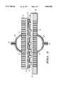
- FIG. 2illustrates an enlarged cross-sectional view of a preferred WLBI assembly according to the present invention.
- FIG. 2shows semiconductor wafer 11 coupled or reversibly attached to a vacuum or hold-down block 17 and probe substrate 12 coupled or reversibly attached to a vacuum or hold-down block 19. With a vacuum applied, vacuum blocks 17 and 19 function, among other things, to overcome the bow problems illustrated in FIG. 1. This minimizes the gaps between corresponding wafer contact portions 13 and probing objects 14.
- FIG. 2further shows removable, non-permanent, or water-soluble Z-axis anisotropically conductive adhesive (ACA) material 21 formed on semiconductor wafer 11.
- Removable Z-axis ACA material 21is a removable polymer composite material including conductive spheres 22 within a water-soluble matrix resin 23.
- FIG. 3illustrates a highly enlarged cross-sectional view of a portion of the WLBI assembly shown in FIG. 2. In particular, FIG. 3, shows conductive spheres 22 substantially aligned along z-axis 24 to provide electrical contact between one of wafer contact portions 13 and one of probing objects 14.
- Removable Z-axis ACA material 21functions, among other things, to overcome the taper and contact non-uniformity problems illustrated in FIG. 1. That is, it functions to create electrical contact between wafer contact portions 13 and probing objects 14.
- water-soluble matrix resin 23preferably has a glass transition temperature (Tg) above the selected burn-in temperature (typically greater than about 85° C.) to produce good Z-axis conductivity. With such a Tg, good Z-axis conductivity is maintained because removable Z-axis ACA material 21 shrinks after a dehydration bake thereby applying a shrinkage or contractive force to semiconductor wafer 11 and probe substrate 12.
- Matrix resin 23comprises a thermoplastic resin (e.g., polyacrylic acid or the like) that is soluble in water.
- matrix resin 23is substantially soluble in water to minimize the need to add organic solvents to dissolve matrix resin 23.
- matrix resin 23is easily removed without damaging semiconductor wafer 11 or probe substrate 12. Also, this allows a manufacturer to easily retrieve and recycle at least a portion of conductive spheres 22 without damaging conductive spheres 22 and without generating hazardous wastes.
- a di-functional monomere.g., butenediol di-glycidyl ether, hexanediol di-glycidyl ether, or the like is added to increase the cross-linking of matrix resin 23.
- Conductive spheres 22typically comprise metal spheres (e.g., gold plated nickel spheres) or metal plated plastic spheres (e.g., gold plated DVB-styrene spheres). Such spheres are available from suppliers such as Zymet Inc. located in East Hanover, N.J.
- the diameter of conductive spheres 22is selected depending upon the pitch or spacing between adjacent wafer contact portions 13.
- conductive spheres 22have a diameter in a range from about 1.0 micron to about 100 microns.
- removable Z-axis ACA material 21is prepared as follows. First about a 5% to about a 25% by weight aqueous solution of polyacrylic acid (PAA) with a molecular weight of about 450,000 grams/mole is prepared (with about a 13% to about a 15% by weight preferred) by dissolving about 0.75 to about 0.85 grams of PAA in about 4.8 to about 5.0 grams of water. Next, bubbles are removed from the aqueous solution using, for example, ultrasound techniques. During the bubble removing process, the aqueous solution becomes clear and has a viscosity on the order of 5,000 centipoise.
- PAApolyacrylic acid
- conductive spheres 22are added to the aqueous solution to provide about a 1% to about a 10% particle loading (with about 5% preferred). For example, about 10 to 11 milligrams (mg) of gold-plated DVB-styrene spheres with a diameter on the order of about 12 microns are added to about 200 mg to about 220 mg of matrix resin 23 to provide removable Z-axis ACA material 21.
- removable Z-axis ACA material 21further includes a modifier (e.g., a water soluble solvent such as propanol) to provide a more uniform film thickness when removable Z-axis ACA material 21 is applied to semiconductor wafer 11.
- a modifiere.g., a water soluble solvent such as propanol
- removable Z-axis ACA material 21further includes an anti-foaming agent (e.g., a silicone defoamer) to reduce foaming.
- removable Z-axis ACA material 21is applied to semiconductor wafer 11.
- removable Z-axis ACA material 21is applied to probe substrate 12.
- removable Z-axis ACA material 21is applied using conventional dispense and spin application techniques.
- removable Z-axis ACA material 21is applied with squeegee or brush application techniques. Such techniques are well known in the art.
- a layer about 20 microns thickis applied. This thickness is adjusted according to the actual thickness Of wafer contact portions 13 and probing objects 14, their thickness variations, and the diameter of conductive spheres 22.
- semiconductor wafer 11is placed into contact with vacuum block 17 and a vacuum is applied to overcome any bow or warp in semiconductor wafer 11.
- probe substrate 12is placed into contact with vacuum block 19 and a vacuum is applied to overcome any bow or warp in probe substrate 12.
- wafer contact portions 13are aligned with the corresponding probing objects 14 and then pressed into contact with each other.
- removable Z-axis ACA material 21functions to fill the gap to provide a conduction path as shown in FIGS. 2 and 3.
- a ball joint device 26(shown in FIG. 2) is attached to either one of or both vacuum blocks 17 and 19.
- ball joint device 26includes a vacuum lock 27 so that once alignment and co-planarity are achieved, ball joint device 26 can be vacuum locked to maintain a desired position.
- the WLBI assemblyis exposed to an appropriate dehydration bake temperature. For example, with the PAA resin material discussed above, the WLBI assembly is exposed to about 95° C. for about 1 to 3 hours in an oven. After the dehydration bake, semiconductor wafer 11 remains in a bonded connection with probe substrate 12.
- This bonded connectionis conductive due to the contractive nature of removable Z-axis ACA material 21 after bake.
- the bonded connectiontypically does not require an external force to maintain.
- a minimal forcee.g., less than about 1 g/wafer contact portion
- prior art clamping devices where about 30 g/wafer contact portion typically is required.
- probe substrate 12includes an edge card connect (not shown), which functions to interface probe substrate 12 to a testing apparatus.
- the IC devices on semiconductor wafer 11are then tested at an elevated temperature under the appropriate bias conditions to screen out any defective devices.
- semiconductor wafer 11is separated from probe substrate 12 by dissolving removable Z-axis ACA material 21 in water.
- removable Z-axis ACA material 21dissolves in about 1.0 to 2.0 hours.
- conductive spheres 22are easily retrieved using filtration, centrifugation, or similar means and can be re-used. This is a significant cost saving feature of the present invention.
- semiconductor wafer 11 and probe substrate 12are separated by heating them to a temperature above the Tg of removable Z-axis ACA material 21. Residual removable Z-axis ACA material 21 is then dissolved in, for example, water.
- semiconductor wafer 11is first brought into alignment and contact with probe substrate 12.
- the space between semiconductor wafer 11 and probe substrate 12is then filled with removable Z-axis ACA material 21.
- Removable Z-axis ACA material 21is then baked and burn-in is carried out as described above.
- the materialincludes water, a matrix resin and a plurality of conductive spheres.
- the materialis suitable for WLBI and greatly simplifies the process by eliminating the need for clamping devices.
- the removable Z-axis ACA materialdoes not require large quantities of organic solvents, which can be hazardous.
- the conductive spheresare easily retrieved and re-used after burn-in thus providing a cost savings.
Landscapes
- Physics & Mathematics (AREA)
- Engineering & Computer Science (AREA)
- General Physics & Mathematics (AREA)
- Condensed Matter Physics & Semiconductors (AREA)
- Manufacturing & Machinery (AREA)
- Computer Hardware Design (AREA)
- Microelectronics & Electronic Packaging (AREA)
- Power Engineering (AREA)
- Testing Of Individual Semiconductor Devices (AREA)
- Testing Or Measuring Of Semiconductors Or The Like (AREA)
Abstract
Description
Claims (7)
Priority Applications (1)
| Application Number | Priority Date | Filing Date | Title |
|---|---|---|---|
| US08/520,118US5661042A (en) | 1995-08-28 | 1995-08-28 | Process for electrically connecting electrical devices using a conductive anisotropic material |
Applications Claiming Priority (1)
| Application Number | Priority Date | Filing Date | Title |
|---|---|---|---|
| US08/520,118US5661042A (en) | 1995-08-28 | 1995-08-28 | Process for electrically connecting electrical devices using a conductive anisotropic material |
Publications (1)
| Publication Number | Publication Date |
|---|---|
| US5661042Atrue US5661042A (en) | 1997-08-26 |
Family
ID=24071274
Family Applications (1)
| Application Number | Title | Priority Date | Filing Date |
|---|---|---|---|
| US08/520,118Expired - LifetimeUS5661042A (en) | 1995-08-28 | 1995-08-28 | Process for electrically connecting electrical devices using a conductive anisotropic material |
Country Status (1)
| Country | Link |
|---|---|
| US (1) | US5661042A (en) |
Cited By (42)
| Publication number | Priority date | Publication date | Assignee | Title |
|---|---|---|---|---|
| US5789278A (en)* | 1996-07-30 | 1998-08-04 | Micron Technology, Inc. | Method for fabricating chip modules |
| US5896038A (en)* | 1996-11-08 | 1999-04-20 | W. L. Gore & Associates, Inc. | Method of wafer level burn-in |
| US5918113A (en)* | 1996-07-19 | 1999-06-29 | Shinko Electric Industries Co., Ltd. | Process for producing a semiconductor device using anisotropic conductive adhesive |
| US6103553A (en)* | 1996-12-11 | 2000-08-15 | Hyundai Electronics Industries Co., Ltd. | Method of manufacturing a known good die utilizing a substrate |
| US6150717A (en)* | 1997-08-04 | 2000-11-21 | Micron Technology, Inc. | Direct die contact (DDC) semiconductor package |
| US6255208B1 (en) | 1999-01-25 | 2001-07-03 | International Business Machines Corporation | Selective wafer-level testing and burn-in |
| US6259036B1 (en) | 1998-04-13 | 2001-07-10 | Micron Technology, Inc. | Method for fabricating electronic assemblies using semi-cured conductive elastomeric bumps |
| US6270363B1 (en) | 1999-05-18 | 2001-08-07 | International Business Machines Corporation | Z-axis compressible polymer with fine metal matrix suspension |
| US6315856B1 (en)* | 1998-03-19 | 2001-11-13 | Kabushiki Kaisha Toshiba | Method of mounting electronic component |
| US6410859B1 (en) | 1995-07-10 | 2002-06-25 | Micron Technology, Inc. | Electrical assembly for semiconductor dice |
| DE10064411A1 (en)* | 2000-12-21 | 2002-06-27 | Giesecke & Devrient Gmbh | Electrically conductive connection between a chip and a coupling element as well as security element, security paper and document of value with such a connection |
| US6451127B1 (en)* | 1999-06-01 | 2002-09-17 | Motorola, Inc. | Conductive paste and semiconductor component having conductive bumps made from the conductive paste |
| US6506978B1 (en)* | 1999-09-03 | 2003-01-14 | Seiko Epson Corporation | Flexible wiring board, electrooptical device and electronic equipment |
| US6518097B1 (en)* | 2000-08-29 | 2003-02-11 | Korea Advanced Institute Of Science And Technology | Method for fabricating wafer-level flip chip package using pre-coated anisotropic conductive adhesive |
| US6582990B2 (en) | 2001-08-24 | 2003-06-24 | International Rectifier Corporation | Wafer level underfill and interconnect process |
| US6627917B1 (en) | 2000-04-25 | 2003-09-30 | Medtronic, Inc. | Method and apparatus for wafer-level burn-in |
| US20030201709A1 (en)* | 2000-04-24 | 2003-10-30 | Nec Corporation | Display panel module with improved bonding structure and method of forming the same |
| US20030205737A1 (en)* | 2000-04-25 | 2003-11-06 | Medtronic, Inc. | Method and apparatus for wafer-level burn-in and testing of integrated circuits |
| US20040212389A1 (en)* | 2003-04-23 | 2004-10-28 | Hamren Steven L. | Method and apparatus for processing semiconductor devices in a singulated form |
| US20050194697A1 (en)* | 2004-03-05 | 2005-09-08 | Miki Hasegawa | Anisotropic conductive sheet and manufacture thereof |
| US20060012333A1 (en)* | 2004-07-15 | 2006-01-19 | John Houldsworth | One time operating state detecting method and apparatus |
| US20070007514A1 (en)* | 2005-07-07 | 2007-01-11 | Horst Groeninger | Method for Contacting Semiconductor Components with a Test Contact |
| US20070187844A1 (en)* | 2006-02-10 | 2007-08-16 | Wintec Industries, Inc. | Electronic assembly with detachable components |
| US7259572B2 (en) | 2004-06-14 | 2007-08-21 | Powerprecise Solutions, Inc. | Method and apparatus for detecting impedance |
| CN100378933C (en)* | 2005-03-14 | 2008-04-02 | 日月光半导体制造股份有限公司 | Method for manufacturing semiconductor packaging structure with laminated crystal cavity |
| US20080081207A1 (en)* | 2006-09-29 | 2008-04-03 | Hisashi Ohsaki | Optical multilayer reflective film, and aligned metal particle film and manufacturing process therefor |
| US20090026612A1 (en)* | 2007-07-27 | 2009-01-29 | Tae Min Kang | Semiconductor package having an improved connection structure and method for manufacturing the same |
| DE102007035903A1 (en)* | 2007-07-31 | 2009-03-12 | Siemens Ag | Contacting foil for the production of electric conductive connection between two points of a carrier, comprises an electrically non-conductive base strip that comprises electric-conductive particles |
| US20100244229A1 (en)* | 2009-03-31 | 2010-09-30 | Stmicroelectronics (Grenoble 2) Sas | Semiconductor package fabrication process and semiconductor package |
| US20110121293A1 (en)* | 2005-02-11 | 2011-05-26 | Kong-Chen Chen | Apparatus and method for predetermined component placement to a target platform |
| US20110147191A1 (en)* | 2009-12-18 | 2011-06-23 | Stmicroelectronics Asia Pacific Pte Ltd. | Methods of using a conductive composite material |
| US20110222253A1 (en)* | 2006-02-10 | 2011-09-15 | Kong-Chen Chen | Electronic assembly with detachable components |
| US20110222252A1 (en)* | 2006-02-10 | 2011-09-15 | Kong-Chen Chen | Electronic assembly with detachable components |
| US20110223695A1 (en)* | 2006-02-10 | 2011-09-15 | Kong-Chen Chen | Electronic assembly with detachable components |
| US20110284262A1 (en)* | 2010-05-21 | 2011-11-24 | Purdue Research Foundation | Controlled Self Assembly of Anisotropic Conductive Adhesives Based on Ferromagnetic Particles |
| US20130032934A1 (en)* | 2011-08-01 | 2013-02-07 | Tessera Inc. | Packaged microelectronic elements having blind vias for heat dissipation |
| US8518304B1 (en) | 2003-03-31 | 2013-08-27 | The Research Foundation Of State University Of New York | Nano-structure enhancements for anisotropic conductive material and thermal interposers |
| US20150048520A1 (en)* | 2013-08-13 | 2015-02-19 | Michael P. Skinner | Magnetic contacts |
| US20150108534A1 (en)* | 2012-09-24 | 2015-04-23 | Xiamen Sanan Optoelectronics Technology Co., Ltd. | Vertical light emitting diode and fabrication method |
| US9365749B2 (en) | 2013-05-31 | 2016-06-14 | Sunray Scientific, Llc | Anisotropic conductive adhesive with reduced migration |
| US9777197B2 (en) | 2013-10-23 | 2017-10-03 | Sunray Scientific, Llc | UV-curable anisotropic conductive adhesive |
| US10396038B2 (en) | 2014-09-26 | 2019-08-27 | Intel Corporation | Flexible packaging architecture |
Citations (16)
| Publication number | Priority date | Publication date | Assignee | Title |
|---|---|---|---|---|
| US4281449A (en)* | 1979-12-21 | 1981-08-04 | Harris Corporation | Method for qualifying biased burn-in integrated circuits on a wafer level |
| US4583042A (en)* | 1983-04-18 | 1986-04-15 | The Boeing Company | Capacitive circuit board testing system and method using a conductive pliant elastomeric reference plane |
| US4705205A (en)* | 1983-06-30 | 1987-11-10 | Raychem Corporation | Chip carrier mounting device |
| US4737112A (en)* | 1986-09-05 | 1988-04-12 | American Telephone And Telegraph Company, At&T Bell Laboratories | Anisotropically conductive composite medium |
| US4968931A (en)* | 1989-11-03 | 1990-11-06 | Motorola, Inc. | Apparatus and method for burning in integrated circuit wafers |
| US5042919A (en)* | 1987-05-01 | 1991-08-27 | Canon Kabushiki Kaisha | External-circuit connecting and packaging structure |
| US5136365A (en)* | 1990-09-27 | 1992-08-04 | Motorola, Inc. | Anisotropic conductive adhesive and encapsulant material |
| US5206585A (en)* | 1991-12-02 | 1993-04-27 | At&T Bell Laboratories | Methods for testing integrated circuit devices |
| US5302854A (en)* | 1990-01-23 | 1994-04-12 | Sumitomo Electric Industries, Ltd. | Packaging structure of a semiconductor device |
| US5317255A (en)* | 1989-09-29 | 1994-05-31 | Soken International Consultants Co., Ltd. | Electric inspection unit using anisotropically electroconductive sheet |
| US5328087A (en)* | 1993-03-29 | 1994-07-12 | Microelectronics And Computer Technology Corporation | Thermally and electrically conductive adhesive material and method of bonding with same |
| US5428190A (en)* | 1993-07-02 | 1995-06-27 | Sheldahl, Inc. | Rigid-flex board with anisotropic interconnect and method of manufacture |
| US5434452A (en)* | 1993-11-01 | 1995-07-18 | Motorola, Inc. | Z-axis compliant mechanical IC wiring substrate and method for making the same |
| US5438223A (en)* | 1992-03-13 | 1995-08-01 | Nitto Denko Corporation | Anisotropic electrically conductive adhesive film and connection structure using the same |
| US5453701A (en)* | 1992-12-23 | 1995-09-26 | Honeywell Inc. | Bare die test and burn-in device |
| US5509815A (en)* | 1994-06-08 | 1996-04-23 | At&T Corp. | Solder medium for circuit interconnection |
- 1995
- 1995-08-28USUS08/520,118patent/US5661042A/ennot_activeExpired - Lifetime
Patent Citations (16)
| Publication number | Priority date | Publication date | Assignee | Title |
|---|---|---|---|---|
| US4281449A (en)* | 1979-12-21 | 1981-08-04 | Harris Corporation | Method for qualifying biased burn-in integrated circuits on a wafer level |
| US4583042A (en)* | 1983-04-18 | 1986-04-15 | The Boeing Company | Capacitive circuit board testing system and method using a conductive pliant elastomeric reference plane |
| US4705205A (en)* | 1983-06-30 | 1987-11-10 | Raychem Corporation | Chip carrier mounting device |
| US4737112A (en)* | 1986-09-05 | 1988-04-12 | American Telephone And Telegraph Company, At&T Bell Laboratories | Anisotropically conductive composite medium |
| US5042919A (en)* | 1987-05-01 | 1991-08-27 | Canon Kabushiki Kaisha | External-circuit connecting and packaging structure |
| US5317255A (en)* | 1989-09-29 | 1994-05-31 | Soken International Consultants Co., Ltd. | Electric inspection unit using anisotropically electroconductive sheet |
| US4968931A (en)* | 1989-11-03 | 1990-11-06 | Motorola, Inc. | Apparatus and method for burning in integrated circuit wafers |
| US5302854A (en)* | 1990-01-23 | 1994-04-12 | Sumitomo Electric Industries, Ltd. | Packaging structure of a semiconductor device |
| US5136365A (en)* | 1990-09-27 | 1992-08-04 | Motorola, Inc. | Anisotropic conductive adhesive and encapsulant material |
| US5206585A (en)* | 1991-12-02 | 1993-04-27 | At&T Bell Laboratories | Methods for testing integrated circuit devices |
| US5438223A (en)* | 1992-03-13 | 1995-08-01 | Nitto Denko Corporation | Anisotropic electrically conductive adhesive film and connection structure using the same |
| US5453701A (en)* | 1992-12-23 | 1995-09-26 | Honeywell Inc. | Bare die test and burn-in device |
| US5328087A (en)* | 1993-03-29 | 1994-07-12 | Microelectronics And Computer Technology Corporation | Thermally and electrically conductive adhesive material and method of bonding with same |
| US5428190A (en)* | 1993-07-02 | 1995-06-27 | Sheldahl, Inc. | Rigid-flex board with anisotropic interconnect and method of manufacture |
| US5434452A (en)* | 1993-11-01 | 1995-07-18 | Motorola, Inc. | Z-axis compliant mechanical IC wiring substrate and method for making the same |
| US5509815A (en)* | 1994-06-08 | 1996-04-23 | At&T Corp. | Solder medium for circuit interconnection |
Non-Patent Citations (2)
| Title |
|---|
| SPIE (The Society of Photo Optical Instumentation Engineers) International Conference and Exhibition; Multichip Modules; Apr. 13 15, 1994, Denver Colorado, vol. 2256, pp. iv viii and 34 40.* |
| SPIE (The Society of Photo-Optical Instumentation Engineers) International Conference and Exhibition; Multichip Modules; Apr. 13-15, 1994, Denver Colorado, vol. 2256, pp. iv-viii and 34-40. |
Cited By (85)
| Publication number | Priority date | Publication date | Assignee | Title |
|---|---|---|---|---|
| US6410859B1 (en) | 1995-07-10 | 2002-06-25 | Micron Technology, Inc. | Electrical assembly for semiconductor dice |
| US5918113A (en)* | 1996-07-19 | 1999-06-29 | Shinko Electric Industries Co., Ltd. | Process for producing a semiconductor device using anisotropic conductive adhesive |
| US5789278A (en)* | 1996-07-30 | 1998-08-04 | Micron Technology, Inc. | Method for fabricating chip modules |
| US6002180A (en)* | 1996-07-30 | 1999-12-14 | Micron Technology, Inc. | Multi chip module with conductive adhesive layer |
| US5896038A (en)* | 1996-11-08 | 1999-04-20 | W. L. Gore & Associates, Inc. | Method of wafer level burn-in |
| US6103553A (en)* | 1996-12-11 | 2000-08-15 | Hyundai Electronics Industries Co., Ltd. | Method of manufacturing a known good die utilizing a substrate |
| US6429453B1 (en) | 1996-12-11 | 2002-08-06 | Hyundai Electronics Industries Co., Ltd. | Substrate assembly for burn in test of integrated circuit chip |
| US6150717A (en)* | 1997-08-04 | 2000-11-21 | Micron Technology, Inc. | Direct die contact (DDC) semiconductor package |
| US6315856B1 (en)* | 1998-03-19 | 2001-11-13 | Kabushiki Kaisha Toshiba | Method of mounting electronic component |
| US6259036B1 (en) | 1998-04-13 | 2001-07-10 | Micron Technology, Inc. | Method for fabricating electronic assemblies using semi-cured conductive elastomeric bumps |
| US6255208B1 (en) | 1999-01-25 | 2001-07-03 | International Business Machines Corporation | Selective wafer-level testing and burn-in |
| US6270363B1 (en) | 1999-05-18 | 2001-08-07 | International Business Machines Corporation | Z-axis compressible polymer with fine metal matrix suspension |
| US6669079B2 (en) | 1999-06-01 | 2003-12-30 | Motorola, Inc. | Conductive paste and semiconductor component having conductive bumps made from the conductive paste |
| US6451127B1 (en)* | 1999-06-01 | 2002-09-17 | Motorola, Inc. | Conductive paste and semiconductor component having conductive bumps made from the conductive paste |
| US6506978B1 (en)* | 1999-09-03 | 2003-01-14 | Seiko Epson Corporation | Flexible wiring board, electrooptical device and electronic equipment |
| US20030201709A1 (en)* | 2000-04-24 | 2003-10-30 | Nec Corporation | Display panel module with improved bonding structure and method of forming the same |
| US6627917B1 (en) | 2000-04-25 | 2003-09-30 | Medtronic, Inc. | Method and apparatus for wafer-level burn-in |
| US20030205737A1 (en)* | 2000-04-25 | 2003-11-06 | Medtronic, Inc. | Method and apparatus for wafer-level burn-in and testing of integrated circuits |
| US6707065B2 (en) | 2000-04-25 | 2004-03-16 | Medtronic, Inc. | Method and apparatus for wafer-level burn-in and testing of integrated circuits |
| US6806494B2 (en) | 2000-04-25 | 2004-10-19 | Medtronic, Inc. | Method and apparatus for wafer-level burn-in and testing of integrated circuits |
| US6518097B1 (en)* | 2000-08-29 | 2003-02-11 | Korea Advanced Institute Of Science And Technology | Method for fabricating wafer-level flip chip package using pre-coated anisotropic conductive adhesive |
| DE10064411A1 (en)* | 2000-12-21 | 2002-06-27 | Giesecke & Devrient Gmbh | Electrically conductive connection between a chip and a coupling element as well as security element, security paper and document of value with such a connection |
| US6967412B2 (en) | 2001-08-24 | 2005-11-22 | International Rectifier Corporation | Wafer level underfill and interconnect process |
| US20030207490A1 (en)* | 2001-08-24 | 2003-11-06 | International Rectifier Corporation | Wafer level underfill and interconnect process |
| CN1327476C (en)* | 2001-08-24 | 2007-07-18 | 国际整流器公司 | Semiconductor device and manufacturing method thereof |
| US6582990B2 (en) | 2001-08-24 | 2003-06-24 | International Rectifier Corporation | Wafer level underfill and interconnect process |
| US8518304B1 (en) | 2003-03-31 | 2013-08-27 | The Research Foundation Of State University Of New York | Nano-structure enhancements for anisotropic conductive material and thermal interposers |
| US20050017739A1 (en)* | 2003-04-23 | 2005-01-27 | Hamren Steven L. | Method and apparatus for processing semiconductor devices in a singulated form |
| US20050042782A1 (en)* | 2003-04-23 | 2005-02-24 | Hamren Steven L. | Method and apparatus for processing semiconductor devices in a singulated form |
| US20050014301A1 (en)* | 2003-04-23 | 2005-01-20 | Hamren Steven L. | Method and apparatus for processing semiconductor devices in a singulated form |
| US7122389B2 (en) | 2003-04-23 | 2006-10-17 | Micron Technology, Inc. | Method for processing semiconductor devices in a singulated form |
| US7126228B2 (en)* | 2003-04-23 | 2006-10-24 | Micron Technology, Inc. | Apparatus for processing semiconductor devices in a singulated form |
| US7129721B2 (en)* | 2003-04-23 | 2006-10-31 | Hamren Steven L | Method and apparatus for processing semiconductor devices in a singulated form |
| US7135345B2 (en) | 2003-04-23 | 2006-11-14 | Micron Technology, Inc. | Methods for processing semiconductor devices in a singulated form |
| US7456504B2 (en) | 2003-04-23 | 2008-11-25 | Micron Technology, Inc. | Electronic component assemblies with electrically conductive bonds |
| US20070155029A1 (en)* | 2003-04-23 | 2007-07-05 | Hamren Steven L | Methods for processing semiconductor devices in a singulated form |
| US20040212389A1 (en)* | 2003-04-23 | 2004-10-28 | Hamren Steven L. | Method and apparatus for processing semiconductor devices in a singulated form |
| US20050194697A1 (en)* | 2004-03-05 | 2005-09-08 | Miki Hasegawa | Anisotropic conductive sheet and manufacture thereof |
| US7304390B2 (en)* | 2004-03-05 | 2007-12-04 | J.S.T. Mfg. Co., Ltd | Anisotropic conductive sheet and manufacture thereof |
| US7259572B2 (en) | 2004-06-14 | 2007-08-21 | Powerprecise Solutions, Inc. | Method and apparatus for detecting impedance |
| US20060012333A1 (en)* | 2004-07-15 | 2006-01-19 | John Houldsworth | One time operating state detecting method and apparatus |
| US7248053B2 (en)* | 2004-07-15 | 2007-07-24 | Powerprecise Solutions, Inc. | One time operating state detecting method and apparatus |
| US20070052422A1 (en)* | 2004-07-15 | 2007-03-08 | John Houldsworth | One time operating state detecting method and apparatus |
| US7589533B2 (en)* | 2004-07-15 | 2009-09-15 | Texas Instruments Northern Virginia Incorporated | One time operating state detecting method and apparatus |
| US20110212549A1 (en)* | 2005-02-11 | 2011-09-01 | Chen Kong C | Apparatus and method for predetermined component placement to a target platform |
| US20110164951A1 (en)* | 2005-02-11 | 2011-07-07 | Wintec Industries, Inc. | Apparatus and method for predetermined component placement to a target platform |
| US8822238B2 (en) | 2005-02-11 | 2014-09-02 | Wintec Industries, Inc. | Apparatus and method for predetermined component placement to a target platform |
| US8674523B2 (en) | 2005-02-11 | 2014-03-18 | Wintec Industries, Inc. | Apparatus and method for predetermined component placement to a target platform |
| US20110210329A1 (en)* | 2005-02-11 | 2011-09-01 | Chen Kong C | Apparatus and method for predetermined component placement to a target platform |
| US9253894B2 (en) | 2005-02-11 | 2016-02-02 | Wintec Industries, Inc. | Electronic assembly with detachable components |
| US8536572B2 (en) | 2005-02-11 | 2013-09-17 | Wintec Industries, Inc. | Assembled multi-component electronic apparatus using alignment and reference marks |
| US20110121293A1 (en)* | 2005-02-11 | 2011-05-26 | Kong-Chen Chen | Apparatus and method for predetermined component placement to a target platform |
| US20110121841A1 (en)* | 2005-02-11 | 2011-05-26 | Kong-Chen Chen | Apparatus and method for predetermined component placement to a target platform |
| US8535955B2 (en) | 2005-02-11 | 2013-09-17 | Wintec Industries, Inc. | Method for assembling a multi-component electronic apparatus |
| US8530248B2 (en) | 2005-02-11 | 2013-09-10 | Wintec Industries, Inc. | Method for placing a component onto a target platform by an apparatus using a probe |
| CN100378933C (en)* | 2005-03-14 | 2008-04-02 | 日月光半导体制造股份有限公司 | Method for manufacturing semiconductor packaging structure with laminated crystal cavity |
| US20070007514A1 (en)* | 2005-07-07 | 2007-01-11 | Horst Groeninger | Method for Contacting Semiconductor Components with a Test Contact |
| US7642104B2 (en)* | 2005-07-07 | 2010-01-05 | Infineon Technologies Ag | Method for contacting semiconductor components with a test contact |
| US20110222253A1 (en)* | 2006-02-10 | 2011-09-15 | Kong-Chen Chen | Electronic assembly with detachable components |
| US20110222252A1 (en)* | 2006-02-10 | 2011-09-15 | Kong-Chen Chen | Electronic assembly with detachable components |
| US20110223695A1 (en)* | 2006-02-10 | 2011-09-15 | Kong-Chen Chen | Electronic assembly with detachable components |
| US20070187844A1 (en)* | 2006-02-10 | 2007-08-16 | Wintec Industries, Inc. | Electronic assembly with detachable components |
| US7955662B2 (en)* | 2006-09-29 | 2011-06-07 | The University Of Tokyo | Optical multilayer reflective film, and aligned metal particle film and manufacturing process therefor |
| US20080081207A1 (en)* | 2006-09-29 | 2008-04-03 | Hisashi Ohsaki | Optical multilayer reflective film, and aligned metal particle film and manufacturing process therefor |
| US20090026612A1 (en)* | 2007-07-27 | 2009-01-29 | Tae Min Kang | Semiconductor package having an improved connection structure and method for manufacturing the same |
| DE102007035903A1 (en)* | 2007-07-31 | 2009-03-12 | Siemens Ag | Contacting foil for the production of electric conductive connection between two points of a carrier, comprises an electrically non-conductive base strip that comprises electric-conductive particles |
| US8372694B2 (en)* | 2009-03-31 | 2013-02-12 | Stmicroelectronics (Grenoble 2) Sas | Semiconductor package fabrication process and semiconductor package |
| US20100244229A1 (en)* | 2009-03-31 | 2010-09-30 | Stmicroelectronics (Grenoble 2) Sas | Semiconductor package fabrication process and semiconductor package |
| US8907692B2 (en)* | 2009-12-18 | 2014-12-09 | Stmicroelectronics Asia Pacific Pte. Ltd. | Methods of using a conductive composite material |
| US20110147191A1 (en)* | 2009-12-18 | 2011-06-23 | Stmicroelectronics Asia Pacific Pte Ltd. | Methods of using a conductive composite material |
| US8816807B2 (en)* | 2010-05-21 | 2014-08-26 | Purdue Research Foundation | Controlled self assembly of anisotropic conductive adhesives based on ferromagnetic particles |
| US20110284262A1 (en)* | 2010-05-21 | 2011-11-24 | Purdue Research Foundation | Controlled Self Assembly of Anisotropic Conductive Adhesives Based on Ferromagnetic Particles |
| US20130032934A1 (en)* | 2011-08-01 | 2013-02-07 | Tessera Inc. | Packaged microelectronic elements having blind vias for heat dissipation |
| US8618647B2 (en)* | 2011-08-01 | 2013-12-31 | Tessera, Inc. | Packaged microelectronic elements having blind vias for heat dissipation |
| US9620433B2 (en) | 2011-08-01 | 2017-04-11 | Tessera, Inc. | Packaged microelectronic elements having blind vias for heat dissipation |
| US20170207141A1 (en)* | 2011-08-01 | 2017-07-20 | Tessera, Inc. | Packaged microelectronic elements having blind vias for heat dissipation |
| US20150108534A1 (en)* | 2012-09-24 | 2015-04-23 | Xiamen Sanan Optoelectronics Technology Co., Ltd. | Vertical light emitting diode and fabrication method |
| US9666757B2 (en)* | 2012-09-24 | 2017-05-30 | Xiamen Sanan Optoelectronics Technology Co., Ltd. | Vertical light emitting diode and fabrication method |
| US9365749B2 (en) | 2013-05-31 | 2016-06-14 | Sunray Scientific, Llc | Anisotropic conductive adhesive with reduced migration |
| US20150048520A1 (en)* | 2013-08-13 | 2015-02-19 | Michael P. Skinner | Magnetic contacts |
| US9142475B2 (en)* | 2013-08-13 | 2015-09-22 | Intel Corporation | Magnetic contacts |
| US9343389B2 (en) | 2013-08-13 | 2016-05-17 | Intel Corporation | Magnetic contacts |
| US9601468B2 (en) | 2013-08-13 | 2017-03-21 | Intel Corporation | Magnetic contacts |
| US9777197B2 (en) | 2013-10-23 | 2017-10-03 | Sunray Scientific, Llc | UV-curable anisotropic conductive adhesive |
| US10396038B2 (en) | 2014-09-26 | 2019-08-27 | Intel Corporation | Flexible packaging architecture |
Similar Documents
| Publication | Publication Date | Title |
|---|---|---|
| US5661042A (en) | Process for electrically connecting electrical devices using a conductive anisotropic material | |
| US6562637B1 (en) | Apparatus and methods of testing and assembling bumped devices using an anisotropically conductive layer | |
| US5854514A (en) | Lead-free interconnection for electronic devices | |
| US5045249A (en) | Electrical interconnection by a composite medium | |
| Kristiansen et al. | Overview of conductive adhesive interconnection technologies for LCDs | |
| KR0140034B1 (en) | Semiconductor wafer storage device, connection method between integrated circuit terminal and probe terminal for inspection of semiconductor wafer and apparatus therefor, inspection method for semiconductor integrated circuit, probe card and manufacturing method thereof | |
| JP2586154B2 (en) | Circuit connection composition, connection method using the same, and semiconductor chip connection structure | |
| KR101130002B1 (en) | Electronic component connecting method and joined body | |
| US5206585A (en) | Methods for testing integrated circuit devices | |
| US6258625B1 (en) | Method of interconnecting electronic components using a plurality of conductive studs | |
| JPH09312176A (en) | Connecting member, and structure and method for connecting electrodes using this connecting member | |
| EP0453147A1 (en) | Testing electronic components | |
| US20040079464A1 (en) | Manufacturing method for electric device | |
| KR19990044151A (en) | Strongly bonded substrate assembly for deformable electronics | |
| JPH08316625A (en) | Method for connecting electrode and connection member used for it | |
| JPH08279371A (en) | Connecting member and connecting structure and connecting method of electrode by using the connecting member | |
| Basavanhally et al. | Direct chip interconnect with adhesive conductor films | |
| US4774768A (en) | Coplanarity tester for surface mounted device | |
| JP4036555B2 (en) | Mounting structure manufacturing method and mounting structure | |
| JP2000082512A (en) | Anisotropic conductive sheet and adapter device for circuit board inspection | |
| JP4223581B2 (en) | Multi-chip mounting method | |
| Park et al. | Chip bonding on non-rigid and flexible substrates with new stepped processes | |
| JPH06275678A (en) | Connecting between chip and substrate using conductive bonding agent improved in repair property | |
| Park et al. | 19.2: Development of a Chip Bonding Technology for Plastic Film LCDs | |
| Matsui et al. | Resin and flexible metal bumps for chip-on-glass technology |
Legal Events
| Date | Code | Title | Description |
|---|---|---|---|
| STCF | Information on status: patent grant | Free format text:PATENTED CASE | |
| FPAY | Fee payment | Year of fee payment:4 | |
| AS | Assignment | Owner name:FREESCALE SEMICONDUCTOR, INC., TEXAS Free format text:ASSIGNMENT OF ASSIGNORS INTEREST;ASSIGNOR:MOTOROLA, INC.;REEL/FRAME:015698/0657 Effective date:20040404 Owner name:FREESCALE SEMICONDUCTOR, INC.,TEXAS Free format text:ASSIGNMENT OF ASSIGNORS INTEREST;ASSIGNOR:MOTOROLA, INC.;REEL/FRAME:015698/0657 Effective date:20040404 | |
| FPAY | Fee payment | Year of fee payment:8 | |
| AS | Assignment | Owner name:CITIBANK, N.A. AS COLLATERAL AGENT, NEW YORK Free format text:SECURITY AGREEMENT;ASSIGNORS:FREESCALE SEMICONDUCTOR, INC.;FREESCALE ACQUISITION CORPORATION;FREESCALE ACQUISITION HOLDINGS CORP.;AND OTHERS;REEL/FRAME:018855/0129 Effective date:20061201 Owner name:CITIBANK, N.A. AS COLLATERAL AGENT,NEW YORK Free format text:SECURITY AGREEMENT;ASSIGNORS:FREESCALE SEMICONDUCTOR, INC.;FREESCALE ACQUISITION CORPORATION;FREESCALE ACQUISITION HOLDINGS CORP.;AND OTHERS;REEL/FRAME:018855/0129 Effective date:20061201 | |
| FPAY | Fee payment | Year of fee payment:12 | |
| AS | Assignment | Owner name:CITIBANK, N.A., AS COLLATERAL AGENT,NEW YORK Free format text:SECURITY AGREEMENT;ASSIGNOR:FREESCALE SEMICONDUCTOR, INC.;REEL/FRAME:024397/0001 Effective date:20100413 Owner name:CITIBANK, N.A., AS COLLATERAL AGENT, NEW YORK Free format text:SECURITY AGREEMENT;ASSIGNOR:FREESCALE SEMICONDUCTOR, INC.;REEL/FRAME:024397/0001 Effective date:20100413 | |
| AS | Assignment | Owner name:CITIBANK, N.A., AS NOTES COLLATERAL AGENT, NEW YORK Free format text:SECURITY AGREEMENT;ASSIGNOR:FREESCALE SEMICONDUCTOR, INC.;REEL/FRAME:030633/0424 Effective date:20130521 Owner name:CITIBANK, N.A., AS NOTES COLLATERAL AGENT, NEW YOR Free format text:SECURITY AGREEMENT;ASSIGNOR:FREESCALE SEMICONDUCTOR, INC.;REEL/FRAME:030633/0424 Effective date:20130521 | |
| AS | Assignment | Owner name:CITIBANK, N.A., AS NOTES COLLATERAL AGENT, NEW YORK Free format text:SECURITY AGREEMENT;ASSIGNOR:FREESCALE SEMICONDUCTOR, INC.;REEL/FRAME:031591/0266 Effective date:20131101 Owner name:CITIBANK, N.A., AS NOTES COLLATERAL AGENT, NEW YOR Free format text:SECURITY AGREEMENT;ASSIGNOR:FREESCALE SEMICONDUCTOR, INC.;REEL/FRAME:031591/0266 Effective date:20131101 | |
| AS | Assignment | Owner name:FREESCALE SEMICONDUCTOR, INC., TEXAS Free format text:PATENT RELEASE;ASSIGNOR:CITIBANK, N.A., AS COLLATERAL AGENT;REEL/FRAME:037354/0225 Effective date:20151207 Owner name:FREESCALE SEMICONDUCTOR, INC., TEXAS Free format text:PATENT RELEASE;ASSIGNOR:CITIBANK, N.A., AS COLLATERAL AGENT;REEL/FRAME:037356/0143 Effective date:20151207 Owner name:FREESCALE SEMICONDUCTOR, INC., TEXAS Free format text:PATENT RELEASE;ASSIGNOR:CITIBANK, N.A., AS COLLATERAL AGENT;REEL/FRAME:037356/0553 Effective date:20151207 | |
| AS | Assignment | Owner name:MORGAN STANLEY SENIOR FUNDING, INC., MARYLAND Free format text:ASSIGNMENT AND ASSUMPTION OF SECURITY INTEREST IN PATENTS;ASSIGNOR:CITIBANK, N.A.;REEL/FRAME:037486/0517 Effective date:20151207 | |
| AS | Assignment | Owner name:MORGAN STANLEY SENIOR FUNDING, INC., MARYLAND Free format text:ASSIGNMENT AND ASSUMPTION OF SECURITY INTEREST IN PATENTS;ASSIGNOR:CITIBANK, N.A.;REEL/FRAME:037518/0292 Effective date:20151207 | |
| AS | Assignment | Owner name:NXP, B.V., F/K/A FREESCALE SEMICONDUCTOR, INC., NETHERLANDS Free format text:RELEASE BY SECURED PARTY;ASSIGNOR:MORGAN STANLEY SENIOR FUNDING, INC.;REEL/FRAME:040925/0001 Effective date:20160912 Owner name:NXP, B.V., F/K/A FREESCALE SEMICONDUCTOR, INC., NE Free format text:RELEASE BY SECURED PARTY;ASSIGNOR:MORGAN STANLEY SENIOR FUNDING, INC.;REEL/FRAME:040925/0001 Effective date:20160912 | |
| AS | Assignment | Owner name:NXP B.V., NETHERLANDS Free format text:RELEASE BY SECURED PARTY;ASSIGNOR:MORGAN STANLEY SENIOR FUNDING, INC.;REEL/FRAME:040928/0001 Effective date:20160622 | |
| AS | Assignment | Owner name:MORGAN STANLEY SENIOR FUNDING, INC., MARYLAND Free format text:CORRECTIVE ASSIGNMENT TO CORRECT THE REMOVE PATENTS 8108266 AND 8062324 AND REPLACE THEM WITH 6108266 AND 8060324 PREVIOUSLY RECORDED ON REEL 037518 FRAME 0292. ASSIGNOR(S) HEREBY CONFIRMS THE ASSIGNMENT AND ASSUMPTION OF SECURITY INTEREST IN PATENTS;ASSIGNOR:CITIBANK, N.A.;REEL/FRAME:041703/0536 Effective date:20151207 | |
| AS | Assignment | Owner name:SHENZHEN XINGUODU TECHNOLOGY CO., LTD., CHINA Free format text:CORRECTIVE ASSIGNMENT TO CORRECT THE TO CORRECT THE APPLICATION NO. FROM 13,883,290 TO 13,833,290 PREVIOUSLY RECORDED ON REEL 041703 FRAME 0536. ASSIGNOR(S) HEREBY CONFIRMS THE THE ASSIGNMENT AND ASSUMPTION OF SECURITYINTEREST IN PATENTS.;ASSIGNOR:MORGAN STANLEY SENIOR FUNDING, INC.;REEL/FRAME:048734/0001 Effective date:20190217 | |
| AS | Assignment | Owner name:MORGAN STANLEY SENIOR FUNDING, INC., MARYLAND Free format text:CORRECTIVE ASSIGNMENT TO CORRECT THE REMOVE APPLICATION11759915 AND REPLACE IT WITH APPLICATION 11759935 PREVIOUSLY RECORDED ON REEL 037486 FRAME 0517. ASSIGNOR(S) HEREBY CONFIRMS THE ASSIGNMENT AND ASSUMPTION OF SECURITYINTEREST IN PATENTS;ASSIGNOR:CITIBANK, N.A.;REEL/FRAME:053547/0421 Effective date:20151207 | |
| AS | Assignment | Owner name:NXP B.V., NETHERLANDS Free format text:CORRECTIVE ASSIGNMENT TO CORRECT THE REMOVEAPPLICATION 11759915 AND REPLACE IT WITH APPLICATION11759935 PREVIOUSLY RECORDED ON REEL 040928 FRAME 0001. ASSIGNOR(S) HEREBY CONFIRMS THE RELEASE OF SECURITYINTEREST;ASSIGNOR:MORGAN STANLEY SENIOR FUNDING, INC.;REEL/FRAME:052915/0001 Effective date:20160622 | |
| AS | Assignment | Owner name:NXP, B.V. F/K/A FREESCALE SEMICONDUCTOR, INC., NETHERLANDS Free format text:CORRECTIVE ASSIGNMENT TO CORRECT THE REMOVEAPPLICATION 11759915 AND REPLACE IT WITH APPLICATION11759935 PREVIOUSLY RECORDED ON REEL 040925 FRAME 0001. ASSIGNOR(S) HEREBY CONFIRMS THE RELEASE OF SECURITYINTEREST;ASSIGNOR:MORGAN STANLEY SENIOR FUNDING, INC.;REEL/FRAME:052917/0001 Effective date:20160912 |