US5659355A - CCD dark mean level correction circuit employing digital processing and analog subtraction requiring no advance knowledge of dark mean level - Google Patents
CCD dark mean level correction circuit employing digital processing and analog subtraction requiring no advance knowledge of dark mean levelDownload PDFInfo
- Publication number
- US5659355A US5659355AUS08/332,215US33221594AUS5659355AUS 5659355 AUS5659355 AUS 5659355AUS 33221594 AUS33221594 AUS 33221594AUS 5659355 AUS5659355 AUS 5659355A
- Authority
- US
- United States
- Prior art keywords
- digital
- pixels
- black
- black level
- interval
- Prior art date
- Legal status (The legal status is an assumption and is not a legal conclusion. Google has not performed a legal analysis and makes no representation as to the accuracy of the status listed.)
- Expired - Fee Related
Links
- 238000012937correctionMethods0.000titledescription7
- 238000012545processingMethods0.000titledescription2
- 238000012935AveragingMethods0.000claimsabstractdescription9
- 238000003384imaging methodMethods0.000abstractdescription6
- 230000008878couplingEffects0.000abstractdescription2
- 238000010168coupling processMethods0.000abstractdescription2
- 238000005859coupling reactionMethods0.000abstractdescription2
- 238000000034methodMethods0.000description6
- 238000010586diagramMethods0.000description5
- 238000009825accumulationMethods0.000description3
- 206010034960PhotophobiaDiseases0.000description2
- 208000013469light sensitivityDiseases0.000description2
- 238000005070samplingMethods0.000description2
- 230000002596correlated effectEffects0.000description1
- 230000000875corresponding effectEffects0.000description1
- 238000001914filtrationMethods0.000description1
- 238000012986modificationMethods0.000description1
- 230000004048modificationEffects0.000description1
- NJPPVKZQTLUDBO-UHFFFAOYSA-NnovaluronChemical compoundC1=C(Cl)C(OC(F)(F)C(OC(F)(F)F)F)=CC=C1NC(=O)NC(=O)C1=C(F)C=CC=C1FNJPPVKZQTLUDBO-UHFFFAOYSA-N0.000description1
- 230000004044responseEffects0.000description1
Images

Classifications
- H—ELECTRICITY
- H04—ELECTRIC COMMUNICATION TECHNIQUE
- H04N—PICTORIAL COMMUNICATION, e.g. TELEVISION
- H04N5/00—Details of television systems
- H04N5/14—Picture signal circuitry for video frequency region
- H04N5/16—Circuitry for reinsertion of DC and slowly varying components of signal; Circuitry for preservation of black or white level
- H04N5/18—Circuitry for reinsertion of DC and slowly varying components of signal; Circuitry for preservation of black or white level by means of "clamp" circuit operated by switching circuit
- H04N5/185—Circuitry for reinsertion of DC and slowly varying components of signal; Circuitry for preservation of black or white level by means of "clamp" circuit operated by switching circuit for the black level
- H—ELECTRICITY
- H04—ELECTRIC COMMUNICATION TECHNIQUE
- H04N—PICTORIAL COMMUNICATION, e.g. TELEVISION
- H04N25/00—Circuitry of solid-state image sensors [SSIS]; Control thereof
- H04N25/60—Noise processing, e.g. detecting, correcting, reducing or removing noise
- H04N25/63—Noise processing, e.g. detecting, correcting, reducing or removing noise applied to dark current
- H04N25/633—Noise processing, e.g. detecting, correcting, reducing or removing noise applied to dark current by using optical black pixels
Definitions
- This inventionrelates, in general, to image signal processing and relates more particularly to the calibration of the black level of an image signal produced by an imaging device (such as a CCD sensor) by means of a digital black clamp circuit.
- an imaging devicesuch as a CCD sensor
- the imaging signal produced by an imaging devicemust be corrected for black level before the image signal is transmitted to a utilization device, such as a video monitor.
- a utilization devicesuch as a video monitor.
- It is known to correct for black level in an analog signalby clamping to the black signal level of the horizontal or vertical blanking period of the video signal (see U.S. Pat. No. 5,142,354, issued Aug. 25, 1992, inventors Suzuki et al.); or through the use of a sample and hold circuit (see U.S. Pat. No. 4,907,084, issued Mar. 7, 1990, inventor Nagafusa).
- Another technique for determining a black level correction signalis to read out image pixels of a imaging sensor when no light is falling on the sensor.
- the dark signal output for each image pixelis then digitized and stored in a black level correction memory.
- the image signal produced by each image pixelis corrected by the stored black level signal generated during the preliminary calibration period (see, for example, U.S. Pat. No. 5,189,528, issued Feb. 23, 1993, inventors Takashima et al.; U.S. Pat. No. 4,974,072, issued Nov. 27, 1990, inventor Hasegawa; and U.S. Pat. No. 5,038,225, issued Aug. 6, 1991; inventor Maeshima).
- U.S. Pat. No. 5,341,218, issued Aug. 23, 1994, inventors Kaneko et al.discloses an interesting digital black level clamping circuit.
- a video signal clamping circuit(capable of maintaining a DC level of a digital video signal at a fixed level) samples the pedestal level of a vertical blanking period of a digital video signal.
- An average value of a plurality of sampling data in a plurality of fieldsis calculated by an average value calculator.
- the average valueis compared with a predetermined clamp level reference value by a comparison output circuit.
- the disclosed circuitis disadvantageous because it (1) clamps to a vertical sync black level, (2) requires the use of a sample and hold circuit, (3) cannot adapt to different analog gains, and (4) uses a complex and expensive ROM difference calculator with associated comparators.
- CCD sensorswhich have a few masked off black pixels at the end or beginning of each line. These pixels are masked off to prevent light sensitivity, but behave like the rest of the pixels with respect to the dark current charge accumulation.
- the black pixelsalso have a similar noise characteristic as the light sensitive ones.
- the values of the black pixelsform a normal, or Gaussian, distribution with a mean value that is very constant and representative of the entire frame.
- the information from the black pixelsis used to set the black level for the whole frame.
- a clamping circuit with low pass filtering and averagingis used to estimate the true black level. The longer the averaging time, the more accurate is the black value obtained, but the response is slower.
- the inventionis applicable to a digital video system. It can quickly obtain a very accurate black level value that can be fed back into a loop to correct image signals.
- the inventionis simple, inexpensive, reliable, and adaptable.
- a digital black clamp circuitcomprising a source of a video signal having a first interval of black level pixels and a second interval of image pixels; a differential amplifier having first and second inputs and an output; wherein said source is coupled to one of said first and second inputs; an analog-to-digital converter (ADC) coupled to said output of said differential amplifier; a digital signal processor coupled to said ADC for accumulating and averaging digital black level pixels in said first interval to produce and average black level signal; a digital-to-analog converter (DAC) coupled to said digital signal processor for converting a digital signal to an analog signal; and a control for selectively uncoupling said DAC to the other of said first and second inputs of said differential amplifier during said first interval of said video signal; and for coupling said DAC to said other of said first and second inputs during said second interval of said video signal to clamp said image pixels to said average black level.
- ADCanalog-to-digital converter
- DACdigital-to-analog converter
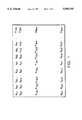
- FIG. 1is a diagrammatic view of an image sensor having masked off black pixels as well as imaging pixels.
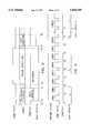
- FIG. 2is a block diagram of a black level clamp circuit according to the present invention.
- FIGS. 3 and 4are respective line timing and frame timing diagrams useful in explaining the operation of the present invention.
- FIG. 1there is shown a diagrammatic illustration of the arrangement of pixels in a CCD sensor having masked off black pixels at the beginning of each line of the sensor.
- the masked pixelsare represented by "b” and image pixels are represented by "a".
- the first linehas black pixels b 11 , b 12 , b 13 , --, b 1l , and image pixels a 11 , a 12 , a 13 , a 14 , --, a 1n .
- the last lineis represented by black pixels b ml to b ml and image pixels are represented by a m1 to a mn .
- lrepresents the number of black pixels in a line, for example, 10;
- nrepresents the number of image pixels in a line; and
- mrepresents the number of lines in the sensor array.
- the black pixels "b”are read out first in each line followed by the image pixels "a". It will be understood that the black pixels "b” may also be located at the end of a line and be read out after the image pixels "a” are read out. As noted above, the black pixels "b” are masked off to prevent light sensitivity, but behave like the rest of the image pixels "a” with respect to the dark current charge accumulation. The black pixels b also have a similar noise characteristic as the light sensitive image pixels a.
- the values of the black pixelsform a normal or Gaussian distribution with a mean value that is very constant and representative of the entire image frame. The information from the black pixels b is used to set the black level for the whole image frame.
- a CCD image sensor 10having masked black pixels as depicted in FIG. 1, images a scene through lens 12 and produces a video signal which is processed by correlator circuit 14 to produce a correlated image signal.
- the image signal channelincludes the difference amplifier 16, gain stage 18, and analog-to-digital converter 20, which converts the analog video signal to a digital video signal.
- the black level pixel signals which are digitized by ADC 20are accumulated and averaged in digital accumulator and averaging circuit 22.
- a very accurate black level valuecan be obtained quickly and fed back into a loop to correct the image signal.
- a switch 28is provided to couple the inverting input of amplifier 16 between ground and the output of DAC 24 by way of potentiometer 26.
- circuit 22measures and averages the black pixel absolute values from the video signal.
- circuit 22measures and averages the black pixel absolute values from the video signal.
- DAC 24is updated with the average digital value of the black pixels.
- Switch 28is moved from the calibrate position to the measure position, and the video out of converter 20 is always measured with respect to the black pixels average value which has been subtracted from the image signal in difference amplifier 16.
- the black pixelsare never sampled with the correction value from DAC 24 in the circuit. This is a unique feature over prior art black level clamping techniques.
- the circuit of FIG. 2does not feed back the correction and measure an error as in a servo system. The only feedback of the correction is for valid video (not the black pixels).
- FIG. 3is a set of timing diagrams which are useful in describing the operation of the circuit of FIG. 2.
- the second timing diagramis of the video signal and shows the black pixel information during the time t 1 to time t 2 .
- the image pixels, or valid video line,continues from t 3 to t 4 .
- FIG. 4is a set of timing diagrams illustrating this implementation.
- the videoneeds to have some black level subtracted from it so that it does not look significantly different from the rest of the lines.
- an averageis taken after the first line and then again after the second, fourth, eighth, and sixteenth lines. Each new average is a little better than the previous because there are more samples taken. After 16 lines, there are 160black pixel samples.
- the DAC 24is updated for the last time and held until the start of the next frame. It does not servo throughout the frame of the video.
- the gainis always set to a constant value during the sampling of black pixels, but during the valid video, the gain switches back to the program value.
Landscapes
- Engineering & Computer Science (AREA)
- Multimedia (AREA)
- Signal Processing (AREA)
- Transforming Light Signals Into Electric Signals (AREA)
Abstract
Description
Claims (2)
Priority Applications (3)
| Application Number | Priority Date | Filing Date | Title |
|---|---|---|---|
| US08/332,215US5659355A (en) | 1994-10-31 | 1994-10-31 | CCD dark mean level correction circuit employing digital processing and analog subtraction requiring no advance knowledge of dark mean level |
| JP7278116AJPH08214220A (en) | 1994-10-31 | 1995-10-25 | Digital black clamp |
| EP95116930AEP0710011A1 (en) | 1994-10-31 | 1995-10-27 | Digital black clamp |
Applications Claiming Priority (1)
| Application Number | Priority Date | Filing Date | Title |
|---|---|---|---|
| US08/332,215US5659355A (en) | 1994-10-31 | 1994-10-31 | CCD dark mean level correction circuit employing digital processing and analog subtraction requiring no advance knowledge of dark mean level |
Publications (1)
| Publication Number | Publication Date |
|---|---|
| US5659355Atrue US5659355A (en) | 1997-08-19 |
Family
ID=23297237
Family Applications (1)
| Application Number | Title | Priority Date | Filing Date |
|---|---|---|---|
| US08/332,215Expired - Fee RelatedUS5659355A (en) | 1994-10-31 | 1994-10-31 | CCD dark mean level correction circuit employing digital processing and analog subtraction requiring no advance knowledge of dark mean level |
Country Status (3)
| Country | Link |
|---|---|
| US (1) | US5659355A (en) |
| EP (1) | EP0710011A1 (en) |
| JP (1) | JPH08214220A (en) |
Cited By (55)
| Publication number | Priority date | Publication date | Assignee | Title |
|---|---|---|---|---|
| WO2000031967A1 (en)* | 1998-11-19 | 2000-06-02 | Sony Corporation | Clamping device and clamping method |
| US20020012127A1 (en)* | 2000-05-18 | 2002-01-31 | Ricoh Company, Ltd. | Image reading device and image forming apparatus |
| US20020190216A1 (en)* | 1999-12-28 | 2002-12-19 | Thierry Ducourant | Method for temperature compensation of an image dectector |
| US20030020818A1 (en)* | 2001-07-25 | 2003-01-30 | Eastman Kodak Company | Median-based dark level acquisition for a frame rate clamp |
| US20030184666A1 (en)* | 2002-03-29 | 2003-10-02 | Wan-Hee Jo | Image sensor having pixel array and method for automatically compensating black level of the same |
| US20030202111A1 (en)* | 2002-04-30 | 2003-10-30 | Jaejin Park | Apparatus and methods for dark level compensation in image sensors using dark pixel sensor metrics |
| US6661929B1 (en)* | 1999-07-14 | 2003-12-09 | Hewlett-Packard Development Company, L.P. | Controlling an imaging array not having black cells using an array controller that is adapted to imaging arrays having black cells |
| US20040051796A1 (en)* | 2002-09-13 | 2004-03-18 | Eastman Kodak Company | Fixed pattern noise removal in CMOS imagers across various operational conditions |
| US6774942B1 (en)* | 2000-08-17 | 2004-08-10 | Exar Corporation | Black level offset calibration system for CCD image digitizer |
| US6774941B1 (en)* | 1999-10-26 | 2004-08-10 | National Semiconductor Corporation | CCD output processing stage that amplifies signals from colored pixels based on the conversion efficiency of the colored pixels |
| US20040155973A1 (en)* | 2003-01-13 | 2004-08-12 | Chang-Min Bea | Image sensor having clamp circuit |
| US6788340B1 (en)* | 1999-03-15 | 2004-09-07 | Texas Instruments Incorporated | Digital imaging control with selective intensity resolution enhancement |
| US6809763B1 (en)* | 1999-08-02 | 2004-10-26 | Olympus Optical Co., Ltd. | Image pickup apparatus and method of correcting deteriorated pixel signal thereof |
| US6839085B1 (en)* | 1999-08-24 | 2005-01-04 | Victor Company Of Japan, Ltd. | Image pickup apparatus for high-speed photographing and method of controlling the same |
| US20050057693A1 (en)* | 2003-09-11 | 2005-03-17 | Sanyo Electric Co.,Ltd. | Digital clamp circuit |
| US20050094009A1 (en)* | 2003-09-04 | 2005-05-05 | Nikon Corporation | Black level correcting device and electronic camera |
| US20060017819A1 (en)* | 1999-08-19 | 2006-01-26 | Canon Kabushiki Kaisha | Image input apparatus |
| US20060044424A1 (en)* | 2004-08-31 | 2006-03-02 | Canon Kabushiki Kaisha | Image signal processing apparatus, image signal processing method and camera using the image signal processing apparatus |
| US20060164688A1 (en)* | 2005-01-26 | 2006-07-27 | Manuel De Pena Alejandro | Ising-model image rendition, and consolidated masking and/or filtering, in incremental printing |
| US7161626B1 (en)* | 1998-10-02 | 2007-01-09 | Ricoh Company, Ltd. | Image reading apparatus |
| US20070268158A1 (en)* | 2006-05-09 | 2007-11-22 | Drivecam, Inc. | System and Method for Reducing Driving Risk With Insight |
| US7317480B1 (en)* | 2000-10-30 | 2008-01-08 | Micron Technology, Inc. | Imaging apparatus providing black level compensation of a successive approximation A/D converter |
| US20080012966A1 (en)* | 2006-07-17 | 2008-01-17 | Jeffery Steven Beck | Image sensor device having improved noise suppression capability and a method for supressing noise in an image sensor device |
| US20080043736A1 (en)* | 2006-08-18 | 2008-02-21 | Drivecam, Inc. | Data Transfer System and Method |
| CN100377569C (en)* | 2004-04-23 | 2008-03-26 | 索尼株式会社 | Optical Black Level Control Circuit |
| US20080273101A1 (en)* | 2007-05-02 | 2008-11-06 | Canon Kabushiki Kaisha | Image capturing system, signal processing circuit, and signal processing method |
| US7536457B2 (en) | 2006-05-08 | 2009-05-19 | Drivecam, Inc. | System and method for wireless delivery of event data |
| US20090237536A1 (en)* | 2008-03-21 | 2009-09-24 | Stmicroelectronics (Research & Development) Limited | Analog-to-digital conversion in image sensors |
| US20090251572A1 (en)* | 2008-04-02 | 2009-10-08 | Chi-Shao Lin | Efficient wide-range and high-resolution black level and offset calibration system |
| US7659827B2 (en) | 2006-05-08 | 2010-02-09 | Drivecam, Inc. | System and method for taking risk out of driving |
| US20100110249A1 (en)* | 2003-10-15 | 2010-05-06 | Sony Corporation | Solid-state imaging device, pixel-signal processing method, analog-signal transferring device, and analog-signal transferring method |
| US20100157035A1 (en)* | 2008-03-21 | 2010-06-24 | Stmicroelectronics (Research & Development) Limited | Analog-to-digital conversion in image sensors |
| US7804426B2 (en) | 2006-05-08 | 2010-09-28 | Drivecam, Inc. | System and method for selective review of event data |
| US20110278652A1 (en)* | 2009-02-12 | 2011-11-17 | Nikon Corporation | Solid state imaging device |
| US8314708B2 (en) | 2006-05-08 | 2012-11-20 | Drivecam, Inc. | System and method for reducing driving risk with foresight |
| US8373567B2 (en) | 2006-05-08 | 2013-02-12 | Drivecam, Inc. | System and method for identifying non-event profiles |
| US8868288B2 (en) | 2006-11-09 | 2014-10-21 | Smartdrive Systems, Inc. | Vehicle exception event management systems |
| US8878965B1 (en)* | 2013-06-26 | 2014-11-04 | Himax Imaging Limited | Black level adjustment device and method for CMOS image sensor |
| US8880279B2 (en) | 2005-12-08 | 2014-11-04 | Smartdrive Systems, Inc. | Memory management in event recording systems |
| US8892310B1 (en) | 2014-02-21 | 2014-11-18 | Smartdrive Systems, Inc. | System and method to detect execution of driving maneuvers |
| US8989959B2 (en) | 2006-11-07 | 2015-03-24 | Smartdrive Systems, Inc. | Vehicle operator performance history recording, scoring and reporting systems |
| US8996240B2 (en) | 2006-03-16 | 2015-03-31 | Smartdrive Systems, Inc. | Vehicle event recorders with integrated web server |
| US9183679B2 (en) | 2007-05-08 | 2015-11-10 | Smartdrive Systems, Inc. | Distributed vehicle event recorder systems having a portable memory data transfer system |
| US9201842B2 (en) | 2006-03-16 | 2015-12-01 | Smartdrive Systems, Inc. | Vehicle event recorder systems and networks having integrated cellular wireless communications systems |
| US9501878B2 (en) | 2013-10-16 | 2016-11-22 | Smartdrive Systems, Inc. | Vehicle event playback apparatus and methods |
| US9554080B2 (en) | 2006-11-07 | 2017-01-24 | Smartdrive Systems, Inc. | Power management systems for automotive video event recorders |
| US9610955B2 (en) | 2013-11-11 | 2017-04-04 | Smartdrive Systems, Inc. | Vehicle fuel consumption monitor and feedback systems |
| US9633318B2 (en) | 2005-12-08 | 2017-04-25 | Smartdrive Systems, Inc. | Vehicle event recorder systems |
| US9663127B2 (en) | 2014-10-28 | 2017-05-30 | Smartdrive Systems, Inc. | Rail vehicle event detection and recording system |
| US9728228B2 (en) | 2012-08-10 | 2017-08-08 | Smartdrive Systems, Inc. | Vehicle event playback apparatus and methods |
| US9836716B2 (en) | 2006-05-09 | 2017-12-05 | Lytx, Inc. | System and method for reducing driving risk with hindsight |
| US10930093B2 (en) | 2015-04-01 | 2021-02-23 | Smartdrive Systems, Inc. | Vehicle event recording system and method |
| US11069257B2 (en) | 2014-11-13 | 2021-07-20 | Smartdrive Systems, Inc. | System and method for detecting a vehicle event and generating review criteria |
| US20210368076A1 (en)* | 2012-07-26 | 2021-11-25 | DePuy Synthes Products, Inc. | Camera system with minimal area monolithic cmos image sensor |
| US11903564B2 (en) | 2013-03-15 | 2024-02-20 | DePuy Synthes Products, Inc. | Image sensor synchronization without input clock and data transmission clock |
Families Citing this family (6)
| Publication number | Priority date | Publication date | Assignee | Title |
|---|---|---|---|---|
| WO1999007138A1 (en)* | 1997-07-31 | 1999-02-11 | Ppt Vision, Inc. | Digital correlated double sample camera |
| GB2386018A (en)* | 2002-02-28 | 2003-09-03 | Qinetiq Ltd | Noise reduction in infra-red imaging arrays using shielded detectors |
| US7259787B2 (en)* | 2003-03-27 | 2007-08-21 | Eastman Kodak Company | Digital black clamp circuit in electronic imaging systems |
| JP2005101870A (en)* | 2003-09-24 | 2005-04-14 | Sanyo Electric Co Ltd | Signal conditioning circuit |
| GB2446844B (en) | 2006-12-05 | 2011-05-25 | Wolfson Microelectronics Plc | Callibration circuit and asociated method |
| US7760258B2 (en)* | 2007-03-07 | 2010-07-20 | Altasens, Inc. | Apparatus and method for stabilizing image sensor black level |
Citations (11)
| Publication number | Priority date | Publication date | Assignee | Title |
|---|---|---|---|---|
| US4786969A (en)* | 1986-04-08 | 1988-11-22 | Sony Corporation | Black level correction circuit for video camera |
| US4907084A (en)* | 1987-08-28 | 1990-03-06 | Asahi Kogaku Kogyo Kabushiki Kaisha | Image reading unit with black level control |
| US4974072A (en)* | 1987-10-14 | 1990-11-27 | Canon Kabushiki Kaisha | Image reading apparatus having a plurality of line sensors and means for correcting crosstalk therebetween |
| US5038225A (en)* | 1986-04-04 | 1991-08-06 | Canon Kabushiki Kaisha | Image reading apparatus with black-level and/or white level correction |
| US5057920A (en)* | 1989-02-28 | 1991-10-15 | Sony Corporation | Video signal clamping circuit operating in the digital domain for removing excess noise on the black level and for providing d c restoration |
| US5105276A (en)* | 1990-11-15 | 1992-04-14 | Eastman Kodak Company | DC restoration of sampled imagery signals |
| US5142354A (en)* | 1989-12-27 | 1992-08-25 | Fuji Photo Optical Co., Ltd. | Signal level correction circuit for a video signal |
| US5189528A (en)* | 1988-09-21 | 1993-02-23 | Fuji Xerox Co., Ltd. | Image reading apparatus |
| US5278658A (en)* | 1990-05-15 | 1994-01-11 | Ricoh Company, Ltd. | Image reading apparatus having a function for correcting dark signals generated in a photoelectric conversion element |
| US5341218A (en)* | 1991-04-09 | 1994-08-23 | Mitsubishi Denki Kabushiki Kaisha | Video signals clamping circuit for maintaining DC level of video signals |
| US5448306A (en)* | 1992-06-30 | 1995-09-05 | Canon Kabushiki Kaisha | Image processing apparatus with variable clamping |
Family Cites Families (4)
| Publication number | Priority date | Publication date | Assignee | Title |
|---|---|---|---|---|
| DE3744076C2 (en)* | 1987-12-24 | 1995-05-11 | Broadcast Television Syst | Method and circuit for black level control of a video signal |
| JPH0229078A (en)* | 1988-07-18 | 1990-01-31 | Sanyo Electric Co Ltd | Picture signal processing circuit |
| JPH0449780A (en)* | 1990-06-18 | 1992-02-19 | Victor Co Of Japan Ltd | Video signal clamping circuit |
| KR0108917Y1 (en)* | 1991-12-05 | 1997-11-08 | Samsung Electronics Co Ltd | Digital clamping circuit |
- 1994
- 1994-10-31USUS08/332,215patent/US5659355A/ennot_activeExpired - Fee Related
- 1995
- 1995-10-25JPJP7278116Apatent/JPH08214220A/enactivePending
- 1995-10-27EPEP95116930Apatent/EP0710011A1/ennot_activeWithdrawn
Patent Citations (11)
| Publication number | Priority date | Publication date | Assignee | Title |
|---|---|---|---|---|
| US5038225A (en)* | 1986-04-04 | 1991-08-06 | Canon Kabushiki Kaisha | Image reading apparatus with black-level and/or white level correction |
| US4786969A (en)* | 1986-04-08 | 1988-11-22 | Sony Corporation | Black level correction circuit for video camera |
| US4907084A (en)* | 1987-08-28 | 1990-03-06 | Asahi Kogaku Kogyo Kabushiki Kaisha | Image reading unit with black level control |
| US4974072A (en)* | 1987-10-14 | 1990-11-27 | Canon Kabushiki Kaisha | Image reading apparatus having a plurality of line sensors and means for correcting crosstalk therebetween |
| US5189528A (en)* | 1988-09-21 | 1993-02-23 | Fuji Xerox Co., Ltd. | Image reading apparatus |
| US5057920A (en)* | 1989-02-28 | 1991-10-15 | Sony Corporation | Video signal clamping circuit operating in the digital domain for removing excess noise on the black level and for providing d c restoration |
| US5142354A (en)* | 1989-12-27 | 1992-08-25 | Fuji Photo Optical Co., Ltd. | Signal level correction circuit for a video signal |
| US5278658A (en)* | 1990-05-15 | 1994-01-11 | Ricoh Company, Ltd. | Image reading apparatus having a function for correcting dark signals generated in a photoelectric conversion element |
| US5105276A (en)* | 1990-11-15 | 1992-04-14 | Eastman Kodak Company | DC restoration of sampled imagery signals |
| US5341218A (en)* | 1991-04-09 | 1994-08-23 | Mitsubishi Denki Kabushiki Kaisha | Video signals clamping circuit for maintaining DC level of video signals |
| US5448306A (en)* | 1992-06-30 | 1995-09-05 | Canon Kabushiki Kaisha | Image processing apparatus with variable clamping |
Cited By (109)
| Publication number | Priority date | Publication date | Assignee | Title |
|---|---|---|---|---|
| US7161626B1 (en)* | 1998-10-02 | 2007-01-09 | Ricoh Company, Ltd. | Image reading apparatus |
| WO2000031967A1 (en)* | 1998-11-19 | 2000-06-02 | Sony Corporation | Clamping device and clamping method |
| US6700609B1 (en) | 1998-11-19 | 2004-03-02 | Sony Corporation | Clamping device and clamping method |
| US6788340B1 (en)* | 1999-03-15 | 2004-09-07 | Texas Instruments Incorporated | Digital imaging control with selective intensity resolution enhancement |
| US6661929B1 (en)* | 1999-07-14 | 2003-12-09 | Hewlett-Packard Development Company, L.P. | Controlling an imaging array not having black cells using an array controller that is adapted to imaging arrays having black cells |
| US6809763B1 (en)* | 1999-08-02 | 2004-10-26 | Olympus Optical Co., Ltd. | Image pickup apparatus and method of correcting deteriorated pixel signal thereof |
| US7053941B1 (en)* | 1999-08-19 | 2006-05-30 | Canon Kabushiki Kaisha | Image input apparatus |
| US20060017819A1 (en)* | 1999-08-19 | 2006-01-26 | Canon Kabushiki Kaisha | Image input apparatus |
| US7542081B2 (en) | 1999-08-19 | 2009-06-02 | Canon Kabushiki Kaisha | Image input apparatus |
| US6839085B1 (en)* | 1999-08-24 | 2005-01-04 | Victor Company Of Japan, Ltd. | Image pickup apparatus for high-speed photographing and method of controlling the same |
| US6774941B1 (en)* | 1999-10-26 | 2004-08-10 | National Semiconductor Corporation | CCD output processing stage that amplifies signals from colored pixels based on the conversion efficiency of the colored pixels |
| US6737654B2 (en)* | 1999-12-28 | 2004-05-18 | Trixell | Method for temperature compensation of an image detector |
| US20020190216A1 (en)* | 1999-12-28 | 2002-12-19 | Thierry Ducourant | Method for temperature compensation of an image dectector |
| US7359099B2 (en)* | 2000-05-18 | 2008-04-15 | Ricoh Company, Ltd. | Image reading device and image forming apparatus |
| US20020012127A1 (en)* | 2000-05-18 | 2002-01-31 | Ricoh Company, Ltd. | Image reading device and image forming apparatus |
| US6774942B1 (en)* | 2000-08-17 | 2004-08-10 | Exar Corporation | Black level offset calibration system for CCD image digitizer |
| US7317480B1 (en)* | 2000-10-30 | 2008-01-08 | Micron Technology, Inc. | Imaging apparatus providing black level compensation of a successive approximation A/D converter |
| US6909460B2 (en)* | 2001-07-25 | 2005-06-21 | Eastman Kodak Company | Median-based dark level acquisition for a frame rate clamp |
| US20030020818A1 (en)* | 2001-07-25 | 2003-01-30 | Eastman Kodak Company | Median-based dark level acquisition for a frame rate clamp |
| US20030184666A1 (en)* | 2002-03-29 | 2003-10-02 | Wan-Hee Jo | Image sensor having pixel array and method for automatically compensating black level of the same |
| US20030202111A1 (en)* | 2002-04-30 | 2003-10-30 | Jaejin Park | Apparatus and methods for dark level compensation in image sensors using dark pixel sensor metrics |
| US20040051796A1 (en)* | 2002-09-13 | 2004-03-18 | Eastman Kodak Company | Fixed pattern noise removal in CMOS imagers across various operational conditions |
| US7443431B2 (en)* | 2002-09-13 | 2008-10-28 | Eastman Kodak Company | Fixed pattern noise removal in CMOS imagers across various operational conditions |
| US7394491B2 (en) | 2003-01-13 | 2008-07-01 | Magnachip Semiconductor, Ltd. | Image sensor having clamp circuit |
| US20040155973A1 (en)* | 2003-01-13 | 2004-08-12 | Chang-Min Bea | Image sensor having clamp circuit |
| US20050094009A1 (en)* | 2003-09-04 | 2005-05-05 | Nikon Corporation | Black level correcting device and electronic camera |
| US7432965B2 (en)* | 2003-09-04 | 2008-10-07 | Nikon Corporation | Black level correcting device and electronic camera |
| US20050057693A1 (en)* | 2003-09-11 | 2005-03-17 | Sanyo Electric Co.,Ltd. | Digital clamp circuit |
| US8004590B2 (en)* | 2003-10-15 | 2011-08-23 | Sony Corporation | Solid-state imaging device, pixel-signal processing method, analog-signal transferring device, and analog-signal transferring method |
| US20100110249A1 (en)* | 2003-10-15 | 2010-05-06 | Sony Corporation | Solid-state imaging device, pixel-signal processing method, analog-signal transferring device, and analog-signal transferring method |
| CN100377569C (en)* | 2004-04-23 | 2008-03-26 | 索尼株式会社 | Optical Black Level Control Circuit |
| US20060044424A1 (en)* | 2004-08-31 | 2006-03-02 | Canon Kabushiki Kaisha | Image signal processing apparatus, image signal processing method and camera using the image signal processing apparatus |
| US8223228B2 (en) | 2004-08-31 | 2012-07-17 | Canon Kabushiki Kaisha | Image signal processing apparatus, image signal processing method and camera using the image signal processing apparatus |
| US20100231762A1 (en)* | 2004-08-31 | 2010-09-16 | Canon Kabushiki Kaisha | Image signal processing apparatus, image signal processing method and camera using the image signal processing apparatus |
| US7750955B2 (en)* | 2004-08-31 | 2010-07-06 | Canon Kabushiki Kaisha | Image signal processing apparatus, image signal processing method and camera using the image signal processing apparatus |
| US8233194B2 (en)* | 2005-01-26 | 2012-07-31 | Hewlett-Packard Development Company, L.P. | Ising-model image rendition, and consolidated masking and/or filtering, in incremental printing |
| US20060164688A1 (en)* | 2005-01-26 | 2006-07-27 | Manuel De Pena Alejandro | Ising-model image rendition, and consolidated masking and/or filtering, in incremental printing |
| US10878646B2 (en) | 2005-12-08 | 2020-12-29 | Smartdrive Systems, Inc. | Vehicle event recorder systems |
| US9226004B1 (en) | 2005-12-08 | 2015-12-29 | Smartdrive Systems, Inc. | Memory management in event recording systems |
| US9911253B2 (en) | 2005-12-08 | 2018-03-06 | Smartdrive Systems, Inc. | Memory management in event recording systems |
| US8880279B2 (en) | 2005-12-08 | 2014-11-04 | Smartdrive Systems, Inc. | Memory management in event recording systems |
| US9633318B2 (en) | 2005-12-08 | 2017-04-25 | Smartdrive Systems, Inc. | Vehicle event recorder systems |
| US9402060B2 (en) | 2006-03-16 | 2016-07-26 | Smartdrive Systems, Inc. | Vehicle event recorders with integrated web server |
| US8996240B2 (en) | 2006-03-16 | 2015-03-31 | Smartdrive Systems, Inc. | Vehicle event recorders with integrated web server |
| US9942526B2 (en) | 2006-03-16 | 2018-04-10 | Smartdrive Systems, Inc. | Vehicle event recorders with integrated web server |
| US10404951B2 (en) | 2006-03-16 | 2019-09-03 | Smartdrive Systems, Inc. | Vehicle event recorders with integrated web server |
| US9208129B2 (en) | 2006-03-16 | 2015-12-08 | Smartdrive Systems, Inc. | Vehicle event recorder systems and networks having integrated cellular wireless communications systems |
| US9472029B2 (en) | 2006-03-16 | 2016-10-18 | Smartdrive Systems, Inc. | Vehicle event recorder systems and networks having integrated cellular wireless communications systems |
| US9201842B2 (en) | 2006-03-16 | 2015-12-01 | Smartdrive Systems, Inc. | Vehicle event recorder systems and networks having integrated cellular wireless communications systems |
| US9545881B2 (en) | 2006-03-16 | 2017-01-17 | Smartdrive Systems, Inc. | Vehicle event recorder systems and networks having integrated cellular wireless communications systems |
| US9566910B2 (en) | 2006-03-16 | 2017-02-14 | Smartdrive Systems, Inc. | Vehicle event recorder systems and networks having integrated cellular wireless communications systems |
| US9691195B2 (en) | 2006-03-16 | 2017-06-27 | Smartdrive Systems, Inc. | Vehicle event recorder systems and networks having integrated cellular wireless communications systems |
| US7804426B2 (en) | 2006-05-08 | 2010-09-28 | Drivecam, Inc. | System and method for selective review of event data |
| US8373567B2 (en) | 2006-05-08 | 2013-02-12 | Drivecam, Inc. | System and method for identifying non-event profiles |
| US8314708B2 (en) | 2006-05-08 | 2012-11-20 | Drivecam, Inc. | System and method for reducing driving risk with foresight |
| US7536457B2 (en) | 2006-05-08 | 2009-05-19 | Drivecam, Inc. | System and method for wireless delivery of event data |
| US7659827B2 (en) | 2006-05-08 | 2010-02-09 | Drivecam, Inc. | System and method for taking risk out of driving |
| US9836716B2 (en) | 2006-05-09 | 2017-12-05 | Lytx, Inc. | System and method for reducing driving risk with hindsight |
| US20070268158A1 (en)* | 2006-05-09 | 2007-11-22 | Drivecam, Inc. | System and Method for Reducing Driving Risk With Insight |
| US10235655B2 (en) | 2006-05-09 | 2019-03-19 | Lytx, Inc. | System and method for reducing driving risk with hindsight |
| US20080012966A1 (en)* | 2006-07-17 | 2008-01-17 | Jeffery Steven Beck | Image sensor device having improved noise suppression capability and a method for supressing noise in an image sensor device |
| US7545418B2 (en)* | 2006-07-17 | 2009-06-09 | Jeffery Steven Beck | Image sensor device having improved noise suppression capability and a method for supressing noise in an image sensor device |
| US20080043736A1 (en)* | 2006-08-18 | 2008-02-21 | Drivecam, Inc. | Data Transfer System and Method |
| US9761067B2 (en) | 2006-11-07 | 2017-09-12 | Smartdrive Systems, Inc. | Vehicle operator performance history recording, scoring and reporting systems |
| US8989959B2 (en) | 2006-11-07 | 2015-03-24 | Smartdrive Systems, Inc. | Vehicle operator performance history recording, scoring and reporting systems |
| US10339732B2 (en) | 2006-11-07 | 2019-07-02 | Smartdrive Systems, Inc. | Vehicle operator performance history recording, scoring and reporting systems |
| US9554080B2 (en) | 2006-11-07 | 2017-01-24 | Smartdrive Systems, Inc. | Power management systems for automotive video event recorders |
| US10682969B2 (en) | 2006-11-07 | 2020-06-16 | Smartdrive Systems, Inc. | Power management systems for automotive video event recorders |
| US10053032B2 (en) | 2006-11-07 | 2018-08-21 | Smartdrive Systems, Inc. | Power management systems for automotive video event recorders |
| US9738156B2 (en) | 2006-11-09 | 2017-08-22 | Smartdrive Systems, Inc. | Vehicle exception event management systems |
| US10471828B2 (en) | 2006-11-09 | 2019-11-12 | Smartdrive Systems, Inc. | Vehicle exception event management systems |
| US8868288B2 (en) | 2006-11-09 | 2014-10-21 | Smartdrive Systems, Inc. | Vehicle exception event management systems |
| US11623517B2 (en) | 2006-11-09 | 2023-04-11 | SmartDriven Systems, Inc. | Vehicle exception event management systems |
| US8072513B2 (en) | 2007-05-02 | 2011-12-06 | Canon Kabushiki Kaisha | Image capturing system, signal processing circuit, and signal processing method |
| US20080273101A1 (en)* | 2007-05-02 | 2008-11-06 | Canon Kabushiki Kaisha | Image capturing system, signal processing circuit, and signal processing method |
| US8456550B2 (en) | 2007-05-02 | 2013-06-04 | Canon Kabushiki Kaisha | Image capturing system for correcting signals output from defective pixels |
| US9679424B2 (en) | 2007-05-08 | 2017-06-13 | Smartdrive Systems, Inc. | Distributed vehicle event recorder systems having a portable memory data transfer system |
| US9183679B2 (en) | 2007-05-08 | 2015-11-10 | Smartdrive Systems, Inc. | Distributed vehicle event recorder systems having a portable memory data transfer system |
| US8305474B2 (en)* | 2008-03-21 | 2012-11-06 | STMicroelectronics (R&D) Ltd. | Analog-to-digital conversion in image sensors |
| US20100157035A1 (en)* | 2008-03-21 | 2010-06-24 | Stmicroelectronics (Research & Development) Limited | Analog-to-digital conversion in image sensors |
| US8134623B2 (en)* | 2008-03-21 | 2012-03-13 | Stmicroelectronics (Research & Development) Ltd. | Analog-to-digital conversion in image sensors using a differential comparison |
| US20090237536A1 (en)* | 2008-03-21 | 2009-09-24 | Stmicroelectronics (Research & Development) Limited | Analog-to-digital conversion in image sensors |
| US20090251572A1 (en)* | 2008-04-02 | 2009-10-08 | Chi-Shao Lin | Efficient wide-range and high-resolution black level and offset calibration system |
| US8643073B2 (en)* | 2009-02-12 | 2014-02-04 | Nikon Corporation | Solid state imaging device |
| US20110278652A1 (en)* | 2009-02-12 | 2011-11-17 | Nikon Corporation | Solid state imaging device |
| USRE46551E1 (en)* | 2009-02-12 | 2017-09-12 | Nikon Corporation | Solid state imaging device |
| USRE47765E1 (en)* | 2009-02-12 | 2019-12-10 | Nikon Corporation | Solid state imaging device |
| USRE49928E1 (en)* | 2009-02-12 | 2024-04-16 | Nikon Corporation | Solid state imaging device |
| US20210368076A1 (en)* | 2012-07-26 | 2021-11-25 | DePuy Synthes Products, Inc. | Camera system with minimal area monolithic cmos image sensor |
| US11766175B2 (en)* | 2012-07-26 | 2023-09-26 | DePuy Synthes Products, Inc. | Camera system with minimal area monolithic CMOS image sensor |
| US9728228B2 (en) | 2012-08-10 | 2017-08-08 | Smartdrive Systems, Inc. | Vehicle event playback apparatus and methods |
| US11903564B2 (en) | 2013-03-15 | 2024-02-20 | DePuy Synthes Products, Inc. | Image sensor synchronization without input clock and data transmission clock |
| US8878965B1 (en)* | 2013-06-26 | 2014-11-04 | Himax Imaging Limited | Black level adjustment device and method for CMOS image sensor |
| US10019858B2 (en) | 2013-10-16 | 2018-07-10 | Smartdrive Systems, Inc. | Vehicle event playback apparatus and methods |
| US9501878B2 (en) | 2013-10-16 | 2016-11-22 | Smartdrive Systems, Inc. | Vehicle event playback apparatus and methods |
| US10818112B2 (en) | 2013-10-16 | 2020-10-27 | Smartdrive Systems, Inc. | Vehicle event playback apparatus and methods |
| US11260878B2 (en) | 2013-11-11 | 2022-03-01 | Smartdrive Systems, Inc. | Vehicle fuel consumption monitor and feedback systems |
| US11884255B2 (en) | 2013-11-11 | 2024-01-30 | Smartdrive Systems, Inc. | Vehicle fuel consumption monitor and feedback systems |
| US9610955B2 (en) | 2013-11-11 | 2017-04-04 | Smartdrive Systems, Inc. | Vehicle fuel consumption monitor and feedback systems |
| US9953470B1 (en) | 2014-02-21 | 2018-04-24 | Smartdrive Systems, Inc. | System and method to detect execution of driving maneuvers |
| US11250649B2 (en) | 2014-02-21 | 2022-02-15 | Smartdrive Systems, Inc. | System and method to detect execution of driving maneuvers |
| US11734964B2 (en) | 2014-02-21 | 2023-08-22 | Smartdrive Systems, Inc. | System and method to detect execution of driving maneuvers |
| US9594371B1 (en) | 2014-02-21 | 2017-03-14 | Smartdrive Systems, Inc. | System and method to detect execution of driving maneuvers |
| US10497187B2 (en) | 2014-02-21 | 2019-12-03 | Smartdrive Systems, Inc. | System and method to detect execution of driving maneuvers |
| US10249105B2 (en) | 2014-02-21 | 2019-04-02 | Smartdrive Systems, Inc. | System and method to detect execution of driving maneuvers |
| US8892310B1 (en) | 2014-02-21 | 2014-11-18 | Smartdrive Systems, Inc. | System and method to detect execution of driving maneuvers |
| US9663127B2 (en) | 2014-10-28 | 2017-05-30 | Smartdrive Systems, Inc. | Rail vehicle event detection and recording system |
| US11069257B2 (en) | 2014-11-13 | 2021-07-20 | Smartdrive Systems, Inc. | System and method for detecting a vehicle event and generating review criteria |
| US10930093B2 (en) | 2015-04-01 | 2021-02-23 | Smartdrive Systems, Inc. | Vehicle event recording system and method |
Also Published As
| Publication number | Publication date |
|---|---|
| JPH08214220A (en) | 1996-08-20 |
| EP0710011A1 (en) | 1996-05-01 |
Similar Documents
| Publication | Publication Date | Title |
|---|---|---|
| US5659355A (en) | CCD dark mean level correction circuit employing digital processing and analog subtraction requiring no advance knowledge of dark mean level | |
| US8553114B2 (en) | Image sensing apparatus and image sensing system | |
| US6774942B1 (en) | Black level offset calibration system for CCD image digitizer | |
| US6791607B1 (en) | Optical black and offset correction in CCD signal processing | |
| US6753913B1 (en) | CMOS analog front end architecture with variable gain for digital cameras and camcorders | |
| KR100753232B1 (en) | Method and apparatus for processing potential signal for image sensor | |
| US6275259B1 (en) | Digital automatic gain control circuit for image system | |
| US7551212B2 (en) | Image pickup apparatus for clamping optical black level to a predetermined level | |
| EP0542995A1 (en) | Self calibrating dual range a/d converter. | |
| JPH08265605A (en) | Imaging device | |
| JPH0738812A (en) | Imaging device equipped with imaging device with multi-channel output | |
| US5455622A (en) | Signal processing apparatus and method for offset compensation of CCD signals | |
| EP0535751B1 (en) | Automatic white balance control apparatus | |
| US5471244A (en) | Automatic dark level zeroing for an analog video signal | |
| EP1944967B1 (en) | System and method for flicker DC offset detection and correction | |
| JPS63308484A (en) | Solid-state image pickup device | |
| JP3212858B2 (en) | Solid-state imaging device | |
| JP3642666B2 (en) | Photometric system | |
| JP2000184294A (en) | Imaging device | |
| JPH05153428A (en) | Clamping circuit | |
| JPH10285432A (en) | Clamp device for video signal | |
| NL192135C (en) | Signal processing device. | |
| KR970004185B1 (en) | Digital clamp system of camcorder | |
| JP3286989B2 (en) | Variable gain control circuit and video camera | |
| JPH10341379A (en) | Image-pickup device and shading correcting method |
Legal Events
| Date | Code | Title | Description |
|---|---|---|---|
| AS | Assignment | Owner name:EASTMAN KODAK COMPANY, NEW YORK Free format text:ASSIGNMENT OF ASSIGNORS INTEREST;ASSIGNORS:BARRON, STEVEN A.;FLOGSTAD, HOKON O.;BLESSINGER, KURT V.;REEL/FRAME:007305/0117 Effective date:19950106 | |
| FEPP | Fee payment procedure | Free format text:PAYOR NUMBER ASSIGNED (ORIGINAL EVENT CODE: ASPN); ENTITY STATUS OF PATENT OWNER: LARGE ENTITY | |
| FEPP | Fee payment procedure | Free format text:PAYER NUMBER DE-ASSIGNED (ORIGINAL EVENT CODE: RMPN); ENTITY STATUS OF PATENT OWNER: LARGE ENTITY Free format text:PAYOR NUMBER ASSIGNED (ORIGINAL EVENT CODE: ASPN); ENTITY STATUS OF PATENT OWNER: LARGE ENTITY | |
| FPAY | Fee payment | Year of fee payment:4 | |
| AS | Assignment | Owner name:ROPINTASSCO HOLDINGS, L.P., GEORGIA Free format text:ASSIGNMENT OF ASSIGNORS INTEREST;ASSIGNOR:REDLAKE MASD, INC.;REEL/FRAME:014822/0001 Effective date:20031128 | |
| AS | Assignment | Owner name:JPMORGAN CHASE BANK, TEXAS Free format text:SECURITY AGREEMENT;ASSIGNOR:ROPINTASSCO HOLDINGS, L.P.;REEL/FRAME:014981/0256 Effective date:20040206 | |
| REMI | Maintenance fee reminder mailed | ||
| LAPS | Lapse for failure to pay maintenance fees | ||
| STCH | Information on status: patent discontinuation | Free format text:PATENT EXPIRED DUE TO NONPAYMENT OF MAINTENANCE FEES UNDER 37 CFR 1.362 | |
| FP | Lapsed due to failure to pay maintenance fee | Effective date:20050819 | |
| AS | Assignment | Owner name:REDLAKE MASD, LLC, CALIFORNIA Free format text:ASSIGNMENT OF ASSIGNORS INTEREST;ASSIGNOR:ROPINTASSCO HOLDINGS, L.P.;REEL/FRAME:017314/0884 Effective date:20060306 | |
| AS | Assignment | Owner name:REDLAKE MASD, LLC, CALIFORNIA Free format text:ASSIGNMENT OF ASSIGNORS INTEREST;ASSIGNOR:ROPINTASSCO HOLDINGS, L.P.;REEL/FRAME:017344/0465 Effective date:20060317 | |
| AS | Assignment | Owner name:ROPINTASSCO HOLDINGS, L.P., FLORIDA Free format text:TERMINATION AND RELEASE OF SECURITY;ASSIGNOR:JPMORGAN CHASE BANK, N.A.;REEL/FRAME:021281/0956 Effective date:20080701 |