US5658710A - Method of making superhard mechanical microstructures - Google Patents
Method of making superhard mechanical microstructuresDownload PDFInfo
- Publication number
- US5658710A US5658710AUS08/395,410US39541095AUS5658710AUS 5658710 AUS5658710 AUS 5658710AUS 39541095 AUS39541095 AUS 39541095AUS 5658710 AUS5658710 AUS 5658710A
- Authority
- US
- United States
- Prior art keywords
- mems
- reacting
- silicon
- gas
- micromachining
- Prior art date
- Legal status (The legal status is an assumption and is not a legal conclusion. Google has not performed a legal analysis and makes no representation as to the accuracy of the status listed.)
- Expired - Fee Related
Links
- 238000004519manufacturing processMethods0.000titleclaimsdescription4
- 229910052710siliconInorganic materials0.000claimsabstractdescription29
- 239000010703siliconSubstances0.000claimsabstractdescription29
- 239000002344surface layerSubstances0.000claimsabstractdescription28
- 239000007789gasSubstances0.000claimsabstractdescription19
- 229910021420polycrystalline siliconInorganic materials0.000claimsabstractdescription17
- 229920005591polysiliconPolymers0.000claimsabstractdescription17
- 239000012528membraneSubstances0.000claimsabstractdescription16
- VNWKTOKETHGBQD-UHFFFAOYSA-NmethaneChemical compoundCVNWKTOKETHGBQD-UHFFFAOYSA-N0.000claimsabstractdescription14
- QGZKDVFQNNGYKY-UHFFFAOYSA-NAmmoniaChemical compoundNQGZKDVFQNNGYKY-UHFFFAOYSA-N0.000claimsabstractdescription11
- 239000000463materialSubstances0.000claimsabstractdescription10
- 150000002430hydrocarbonsChemical class0.000claimsabstractdescription8
- 238000005459micromachiningMethods0.000claimsabstractdescription8
- 239000004215Carbon black (E152)Substances0.000claimsabstractdescription7
- 229930195733hydrocarbonNatural products0.000claimsabstractdescription7
- OTMSDBZUPAUEDD-UHFFFAOYSA-NEthaneChemical compoundCCOTMSDBZUPAUEDD-UHFFFAOYSA-N0.000claimsabstractdescription4
- HSFWRNGVRCDJHI-UHFFFAOYSA-Nalpha-acetyleneNatural productsC#CHSFWRNGVRCDJHI-UHFFFAOYSA-N0.000claimsabstractdescription4
- 125000002534ethynyl groupChemical group[H]C#C*0.000claimsabstractdescription4
- 238000000034methodMethods0.000claimsdescription49
- 229910010271silicon carbideInorganic materials0.000claimsdescription21
- HBMJWWWQQXIZIP-UHFFFAOYSA-Nsilicon carbideChemical compound[Si+]#[C-]HBMJWWWQQXIZIP-UHFFFAOYSA-N0.000claimsdescription20
- 239000000758substrateSubstances0.000claimsdescription12
- 238000000576coating methodMethods0.000claimsdescription11
- 239000011248coating agentSubstances0.000claimsdescription10
- IJGRMHOSHXDMSA-UHFFFAOYSA-NAtomic nitrogenChemical compoundN#NIJGRMHOSHXDMSA-UHFFFAOYSA-N0.000claimsdescription9
- 229910052581Si3N4Inorganic materials0.000claimsdescription9
- HQVNEWCFYHHQES-UHFFFAOYSA-Nsilicon nitrideChemical compoundN12[Si]34N5[Si]62N3[Si]51N64HQVNEWCFYHHQES-UHFFFAOYSA-N0.000claimsdescription8
- KRHYYFGTRYWZRS-UHFFFAOYSA-NFluoraneChemical compoundFKRHYYFGTRYWZRS-UHFFFAOYSA-N0.000claimsdescription7
- ATUOYWHBWRKTHZ-UHFFFAOYSA-NPropaneChemical compoundCCCATUOYWHBWRKTHZ-UHFFFAOYSA-N0.000claimsdescription6
- 150000001875compoundsChemical class0.000claimsdescription6
- OKTJSMMVPCPJKN-UHFFFAOYSA-NCarbonChemical compound[C]OKTJSMMVPCPJKN-UHFFFAOYSA-N0.000claimsdescription4
- UFHFLCQGNIYNRP-UHFFFAOYSA-NHydrogenChemical compound[H][H]UFHFLCQGNIYNRP-UHFFFAOYSA-N0.000claimsdescription4
- 229910052799carbonInorganic materials0.000claimsdescription4
- 230000000873masking effectEffects0.000claimsdescription4
- 229910052757nitrogenInorganic materials0.000claimsdescription4
- 239000007787solidSubstances0.000claimsdescription4
- VYPSYNLAJGMNEJ-UHFFFAOYSA-NSilicium dioxideChemical compoundO=[Si]=OVYPSYNLAJGMNEJ-UHFFFAOYSA-N0.000claimsdescription3
- 125000004432carbon atomChemical groupC*0.000claimsdescription3
- 239000001294propaneSubstances0.000claimsdescription3
- DDFHBQSCUXNBSA-UHFFFAOYSA-N5-(5-carboxythiophen-2-yl)thiophene-2-carboxylic acidChemical compoundS1C(C(=O)O)=CC=C1C1=CC=C(C(O)=O)S1DDFHBQSCUXNBSA-UHFFFAOYSA-N0.000claimsdescription2
- 125000004433nitrogen atomChemical groupN*0.000claimsdescription2
- 125000004429atomChemical group0.000claims3
- 229910052814silicon oxideInorganic materials0.000claims1
- 238000004630atomic force microscopyMethods0.000abstractdescription6
- 229910007277Si3 N4Inorganic materials0.000abstractdescription4
- 239000000126substanceSubstances0.000abstractdescription2
- XUIMIQQOPSSXEZ-UHFFFAOYSA-NSiliconChemical compound[Si]XUIMIQQOPSSXEZ-UHFFFAOYSA-N0.000description26
- 238000006243chemical reactionMethods0.000description14
- 239000010410layerSubstances0.000description8
- 230000015572biosynthetic processEffects0.000description7
- 150000004767nitridesChemical class0.000description6
- 235000012431wafersNutrition0.000description6
- 238000005530etchingMethods0.000description5
- 239000004065semiconductorSubstances0.000description4
- 229910021529ammoniaInorganic materials0.000description3
- 230000003647oxidationEffects0.000description3
- 238000007254oxidation reactionMethods0.000description3
- 239000000523sampleSubstances0.000description3
- 238000007493shaping processMethods0.000description3
- 230000008021depositionEffects0.000description2
- 238000005516engineering processMethods0.000description2
- 239000001257hydrogenSubstances0.000description2
- 229910052739hydrogenInorganic materials0.000description2
- 150000002500ionsChemical class0.000description2
- 229910021421monocrystalline siliconInorganic materials0.000description2
- NJPPVKZQTLUDBO-UHFFFAOYSA-NnovaluronChemical compoundC1=C(Cl)C(OC(F)(F)C(OC(F)(F)F)F)=CC=C1NC(=O)NC(=O)C1=C(F)C=CC=C1FNJPPVKZQTLUDBO-UHFFFAOYSA-N0.000description2
- 238000001020plasma etchingMethods0.000description2
- LIVNPJMFVYWSIS-UHFFFAOYSA-Nsilicon monoxideChemical compound[Si-]#[O+]LIVNPJMFVYWSIS-UHFFFAOYSA-N0.000description2
- XLYOFNOQVPJJNP-UHFFFAOYSA-NwaterChemical compoundOXLYOFNOQVPJJNP-UHFFFAOYSA-N0.000description2
- ZOXJGFHDIHLPTG-UHFFFAOYSA-NBoronChemical compound[B]ZOXJGFHDIHLPTG-UHFFFAOYSA-N0.000description1
- 229910000831SteelInorganic materials0.000description1
- 230000003213activating effectEffects0.000description1
- 125000001931aliphatic groupChemical group0.000description1
- QVGXLLKOCUKJST-UHFFFAOYSA-Natomic oxygenChemical compound[O]QVGXLLKOCUKJST-UHFFFAOYSA-N0.000description1
- 229910052796boronInorganic materials0.000description1
- 239000012159carrier gasSubstances0.000description1
- 230000001419dependent effectEffects0.000description1
- 229910001873dinitrogenInorganic materials0.000description1
- 238000007598dipping methodMethods0.000description1
- 230000005684electric fieldEffects0.000description1
- 230000003628erosive effectEffects0.000description1
- 239000012530fluidSubstances0.000description1
- 238000010438heat treatmentMethods0.000description1
- 229910000040hydrogen fluorideInorganic materials0.000description1
- 230000002209hydrophobic effectEffects0.000description1
- 238000007654immersionMethods0.000description1
- 230000003116impacting effectEffects0.000description1
- 238000001802infusionMethods0.000description1
- 239000004615ingredientSubstances0.000description1
- 238000009413insulationMethods0.000description1
- 239000012212insulatorSubstances0.000description1
- 238000010884ion-beam techniqueMethods0.000description1
- 230000008018meltingEffects0.000description1
- 238000002844meltingMethods0.000description1
- 239000000203mixtureSubstances0.000description1
- 239000002052molecular layerSubstances0.000description1
- QJGQUHMNIGDVPM-UHFFFAOYSA-Nnitrogen groupChemical group[N]QJGQUHMNIGDVPM-UHFFFAOYSA-N0.000description1
- 229910000069nitrogen hydrideInorganic materials0.000description1
- 230000003287optical effectEffects0.000description1
- 239000001301oxygenSubstances0.000description1
- 229910052760oxygenInorganic materials0.000description1
- 238000000206photolithographyMethods0.000description1
- 239000000376reactantSubstances0.000description1
- 230000035484reaction timeEffects0.000description1
- 238000004626scanning electron microscopyMethods0.000description1
- -1silicon nitride compoundChemical class0.000description1
- 239000007858starting materialSubstances0.000description1
- 239000010959steelSubstances0.000description1
Images


Classifications
- G—PHYSICS
- G01—MEASURING; TESTING
- G01Q—SCANNING-PROBE TECHNIQUES OR APPARATUS; APPLICATIONS OF SCANNING-PROBE TECHNIQUES, e.g. SCANNING PROBE MICROSCOPY [SPM]
- G01Q70/00—General aspects of SPM probes, their manufacture or their related instrumentation, insofar as they are not specially adapted to a single SPM technique covered by group G01Q60/00
- G01Q70/16—Probe manufacture
- B—PERFORMING OPERATIONS; TRANSPORTING
- B81—MICROSTRUCTURAL TECHNOLOGY
- B81C—PROCESSES OR APPARATUS SPECIALLY ADAPTED FOR THE MANUFACTURE OR TREATMENT OF MICROSTRUCTURAL DEVICES OR SYSTEMS
- B81C1/00—Manufacture or treatment of devices or systems in or on a substrate
- B81C1/00642—Manufacture or treatment of devices or systems in or on a substrate for improving the physical properties of a device
- B81C1/0065—Mechanical properties
- B81C1/00682—Treatments for improving mechanical properties, not provided for in B81C1/00658 - B81C1/0065
- B—PERFORMING OPERATIONS; TRANSPORTING
- B82—NANOTECHNOLOGY
- B82Y—SPECIFIC USES OR APPLICATIONS OF NANOSTRUCTURES; MEASUREMENT OR ANALYSIS OF NANOSTRUCTURES; MANUFACTURE OR TREATMENT OF NANOSTRUCTURES
- B82Y35/00—Methods or apparatus for measurement or analysis of nanostructures
- G—PHYSICS
- G01—MEASURING; TESTING
- G01Q—SCANNING-PROBE TECHNIQUES OR APPARATUS; APPLICATIONS OF SCANNING-PROBE TECHNIQUES, e.g. SCANNING PROBE MICROSCOPY [SPM]
- G01Q70/00—General aspects of SPM probes, their manufacture or their related instrumentation, insofar as they are not specially adapted to a single SPM technique covered by group G01Q60/00
- G01Q70/08—Probe characteristics
- G01Q70/14—Particular materials
- H—ELECTRICITY
- H01—ELECTRIC ELEMENTS
- H01J—ELECTRIC DISCHARGE TUBES OR DISCHARGE LAMPS
- H01J9/00—Apparatus or processes specially adapted for the manufacture, installation, removal, maintenance of electric discharge tubes, discharge lamps, or parts thereof; Recovery of material from discharge tubes or lamps
- H01J9/02—Manufacture of electrodes or electrode systems
- H01J9/022—Manufacture of electrodes or electrode systems of cold cathodes
- H01J9/025—Manufacture of electrodes or electrode systems of cold cathodes of field emission cathodes
- B—PERFORMING OPERATIONS; TRANSPORTING
- B81—MICROSTRUCTURAL TECHNOLOGY
- B81B—MICROSTRUCTURAL DEVICES OR SYSTEMS, e.g. MICROMECHANICAL DEVICES
- B81B2201/00—Specific applications of microelectromechanical systems
- B81B2201/12—STM or AFM microtips
- H—ELECTRICITY
- H01—ELECTRIC ELEMENTS
- H01J—ELECTRIC DISCHARGE TUBES OR DISCHARGE LAMPS
- H01J2209/00—Apparatus and processes for manufacture of discharge tubes
- H01J2209/02—Manufacture of cathodes
- H01J2209/022—Cold cathodes
- H01J2209/0223—Field emission cathodes
- H01J2209/0226—Sharpening or resharpening of emitting point or edge
Definitions
- the inventionrelates to microminiature mechanical structures such as hinges, cantilevers, actuators, sensors, diaphragms, and membranes.
- MEMSMechanical microstructures
- gears and leverswhich may be combined to create complex, yet tiny machines.
- Such microstructuresneed not be limited to mechanical tools.
- a tiny membranecan be employed as a sensor of differential gas pressures by measuring a capacitance between that membrane and an adjacent surface.
- tiny cantileverscan be actuated via an applied electrical force to control valves for fluid flow.
- Other known microstructuresinclude sharply pointed tips for microprobes used in atomic force microscopy or for field emitting structures.
- MEMScan differ from larger, more commonplace machines in structure, method of formation and method of use.
- MEMSare fabricated with technologies developed for semiconductor processing, such as etching of silicon, because tools that are used for production of larger machines do not allow for the fine micromachining necessary to create MEMS.
- MEMS created from silicon or polysilicon substrateshave characteristics derived from those materials. The substrates are hard, though brittle, and can be micromachined to create structures with submicron features.
- silicon and polysiliconare also fairly reactive, and if left exposed to air quickly form a silicon monoxide or dioxide surface layer which is weaker than the starting materials and which continues to grow into the substrate.
- the above objectis achieved by forming a superhard and inert surface layer or skin on a silicon or polysilicon microstructure.
- a superhard and inert surface layer or skinmay be as thin as a mono-molecular layer and as thick as the entire microstructure. Since mechanical failures of microstructures commonly begin at the surface and propagate through or along the structure, having a superhard skin increases the strength of the entire structure. Providing an inert skin to a microstructure prevents a gradual erosion of the structure due to oxidation of the surface layer. This procedure is similar to the surface hardening of steel for larger structures.
- the hard and inert surface layer of the present inventionis formed by first forming a micromechanical structure in silicon or polysilicon by conventional semiconductor processes such as photolithography and etching.
- the resulting microstructure, or array of microstructures on a waferis then reacted at an elevated temperature with a hydrocarbon or ammonia gas so that carbon or nitrogen atoms from the gas diffuse into a surface layer of the structure., forming a silicon carbide or silicon nitride compound, respectively, in the surface layer.
- Conversion of the surface layer in a gaseous ambientis different than coating the surface with a layer of carbide or nitride.
- the layering processes of the prior artyielded more rounded edges, tips and corners.
- the infusion of carbon or nitrogen into the surface layer of silicon or polysilicontakes place at temperatures appreciably below the melting point of silicon and polysilicon and below a temperature at which these materials become soft. It is important to remove any native oxides that have formed on the surface of the microstructure prior to converting the surface layer to silicon carbide or silicon nitride. This stripping of native oxides can be accomplished by dipping in a 10:1 solution of DI water and hydrofluoric acid, or by exposing the structure to hydrogen gas at temperatures of 700° C. to 950° C.
- Either the whole or a part of a microstructuremay be converted into derivatives of Si having superior hardness properties.
- Another advantage of SiC surface layers for MEMsis that the surface layers are sufficiently conductive to bleed off charge acquired by friction, are much more inert, and less likely to collect moisture. These properties decrease the sticking (less stiction) usually observed in microstructures. Thus, conversion changes physical, electrical and chemical properties of the base material.
- FIGS. 1 and 2are scanning electron microscopy pictures of a micro-probe tip made in accord with the present invention.
- FIG. 3is a plan view of a micro-probe tip in accord with the present invention.
- FIG. 4is a top view of a micromachined pivoting mirror having hinges which have been reacted in accord with the present invention.
- FIG. 5is a cross-sectional view of a membrane which has been reacted in accord with the present invention.
- a silicon tip on a silicon cantilever substratesuch as may be employed in atomic force microscopy (AFM) is first made in a conventional process, for example as described in U.S. Pat. No. 4,968,585 to the point of forming silicon posts with any cap removed.
- This processinvolves use of semiconductor masking and etching techniques.
- a desired cantilever sectionis laid out on a solid silicon wafer with an integral tip section. Silicon is etched away in the cantilever section leaving a post at the tip section. The post is then sharpened using the technique described by Marcus et al. in Applied Physics Letters 56, no. 3, p. 226 (1990) until a high aspect ratio tip is formed.
- a high aspect ratiois commonly defined as the length of the tip exceeding the dimension of the base by at least five times.
- the technique of Marcus et al.involves repeated oxidation and removal of oxide.
- the present inventionis not limited to this method, and may be used with any process that produces a tip, with a shape roughly suited to AFM before final shaping.
- Final shapingmay be by any suitable method such as ion beam etching of silicon or polysilicon, reactive ion or plasma etching or various wet etch processes, including electrochemical processes.
- the tipwhich is free from oxide at this point, is placed in a reactive environment, generally at a pressure of 10 -7 to 5 ⁇ 10 -2 Torr and at a temperature in a range of 700° C. to 1100° C., but preferably in the 700° C. to 950° C. range.
- the surface of the silicon or polysilicon, or other base materialis converted into the material of choice.
- the exact temperature employedinvolves a tradeoff between the thickness of the converted layer and the sharpness of the tip. Sharper tips are maintained at lower reaction temperatures.
- As the tip is very thinit is possible to convert the critical parts of the tip completely, if so desired, while coating the rest of it with a layer of the reactant material.
- the conversion processis not dependent on the shaping process which is used. For the situation in which the surface layer to be converted has been exposed to air, it is important to remove any native oxides which have formed on the surface.
- an array of such tipscan be formed on a surface for field emission from the tips.
- an array of silicon tipsmay be formed as described in U.S. Pat. No. 5,201,992 to Marcus et al.
- the tipsare exposed to a hydrocarbon gas such as methane, ethane, or propane at an elevated temperature preferably in the range of 700° C. to 950° C., at an atmosphere of 10 -7 to 5 ⁇ 10 -2 Torr for one to twenty minutes, as described above.
- the carbon atoms from the hydrocarbon gasdiffuse into the surface layer of the tips to form a silicon carbide surface layer, leaving the shape of the tips essentially unchanged.
- Such electrically conductive tipshave an advantage when used in field emission due to their sharpness, which promotes electron emission, and their hardness, which minimizes damage from impacting ions, thereby extending their life.
- SiC tipscan also be formed using acetylene or almost any aliphatic gaseous compound, rather than methane or ethane, as the organic reactive gas.
- the method of C. J. Mogab and H. J. Leamy, described in Applied Physics Letters, 45, no. 3, p. 1075 (1974)relates to conversion of monocrystalline silicon to ⁇ -silicon carbide using acetylene in a vacuum of 10 -7 to 5 ⁇ 10 -4 Torr at temperatures between 800° and 1100° C.
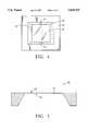
- FIGS. 1 and 2show a SiC tip made in accord with the present invention using the procedure of Mogab et al., except using propane C 3 H 8 , as the organic reactive gas.
- FIG. 1shows a thinned tip before reacting with the gas.
- FIG. 2shows the same tip after the reacting step.
- the tiphas sides that arch upwardly following a curve that appears exponentially steep at the center.
- the height of the tipis more than 5 micrometers and the base dimension is about one micrometer.
- outer zones 13 of tip 11are reacted to form SiC.
- the dimensions A and Bare 200 ⁇ each.
- a rounded tipmay form at apex region 15 having an estimated radius of about 100 ⁇ indicated by arrow R, but conditions for forming rounded tips are not understood and rounding cannot be predicted. The rounding of the tip would give the tip a stylus quality, avoiding tendency to fracture if the tip tapered to a hair-like point, as well as reducing the tendency to stick to material.
- An unreacted silicon zone 17lies beneath the reacted regions.
- the length of the completely converted portionis about 500 ⁇ . Very short reaction times of a few minutes are all that is required to provide almost complete conversion.
- RTArapid thermal anneal stations
- oxidation or nitridation systemsor other CVD reactors by using the appropriate ambient.
- an application of a 10:1 solution of DI water and hydrofluoric acidmay be used, or the oxides may be removed by heating in hydrogen gas at 700° C. to 950° C. at a pressure in the range of a fraction of a milli-Torr to a few milli-Torr, e.g. from 10 -5 to 10 -2 Torr.
- a solution of ammonium fluoride or vaporous hydrogen fluoridemay be used.
- FIG. 4a movable micromechanical mirror 20 is shown within a section 22 of a silicon wafer.
- a waferhas been etched to define torsional support bars or hinges 25 and 27 connecting the mirror 20 to the section 22.
- electrodes 29 and 30Mounted below the wafer and spaced slightly from the mirror 20 are electrodes 29 and 30. These electrodes will be alternately charged by voltages which cause electric fields to attract one side or another of the mirror 20, causing the mirror to pivot and thereby changing the direction at which light is reflected.
- the hinges 25 and 27are thus frequently twisted in operation, causing stresses and strains that can damage the hinges and lead to failure of the mirror 20.
- the hinges 25 and 27are reacted using the process of the present invention in an organic gas at an elevated temperature, so that carbon atoms diffuse into a surface layer of the hinges and form a tough skin of silicon carbide.
- the mirror 20has been masked with an oxide or nitride coating to keep the mirror surface free from carbide formation.
- the temperatureis lowered, and the oxide or nitride is stripped from the mirror 20 to leave a flat, reflective surface of silicon.
- the gas reaction process of the present inventionallows a tough silicon carbide surface layer to be formed in a gentle manner surrounding the hinges 25 and 27, including areas that would be difficult to reach without causing damage using other methods.
- the stripping or unmasking of the oxide or nitride coatingis well known in the art.
- FIG. 5shows a thin membrane 50 from 500 ⁇ to 50 microns thick formed from a solid silicon or polysilicon substrate 35.
- Membrane 50may be used as a window or as part of a pressure transducer or microphone.
- Membrane 50may be made with a variety of fabrication techniques known in the art such as anisotropic etching, using Simox or bonded wafers, electrochemical etch stops, or boron doping.
- Such membranesmay be under very high stress, especially when used as atmospheric windows to hold off pressure against a vacuum. They may also need some protection from reactive ingredients in the atmosphere.
- membrane 50By immersion of membrane 50 in a gaseous hydrocarbon atmosphere ranging from 10 -7 to 5 ⁇ 10 -2 Torr and 700° to 1100° C., it is possible to form very thin layers of silicon carbide on both sides 33 and 44 of membrane 50, after membrane 50 is formed. If only one sided deposition on the membrane is desired, the same technique can be used before membrane formation, e.g. by reacting side 33 of substrate 35 and then forming membrane 50.
- the temperature range for depositionmay be slightly higher than for structures such as tips, because there is no danger of losing the sharp points which are desired in carbide tip formation.
- Such proceduresmay also be used for deformable optical grating modulators, actuators, relays, cantilevers, gears, motors, gimbals, etc., which may be made out of silicon or polysilicon.
- Surface wearis also reduced by the formation of very hard surface layers.
- the methods of the present inventiongreatly help in eliminating stiction that may take place in these devices where moisture tends to collect.
- Silicon carbideis relatively hydrophobic as compared to silicon and polysilicon.
- a hard finishinvolves Si 3 N 4 .
- silicon nitridean appropriate source of nitrogen such as ammonia needs to be used. Because of its relative stability, nitrogen gas, although usable, is less desirable as it does not decompose readily.
- the superhard finishcan also be prepared by plasma anodic nitridation in a nitrogen-hydrogen plasma at lower temperatures (700°-900° C.), or in an ammonia plasma. In plasma nitridation, the silicon or polysilicon tip is placed in a vacuum chamber in the vicinity of a pair of electrodes. A nitrogen-containing gas, such as ammonia, NH 3 is introduced into the chamber.
- a gas ionizing, AC voltageis applied to the electrodes, activating the ionized gas and accelerating ions through the chamber, some of which will encounter the tip and react with the silicon or polysilicon to form a hard and tough Si 3 N 4 layer having a thickness of at least 100 ⁇ .
- Thermal nitridationis a well established technology in the semiconductor industry. It provides for very good quality, but usually very thin (50-100 ⁇ ) films, as the growth kinetics are self-limiting. For selective positioning of a silicon nitride finish, masking with an oxide coating is appropriate.
- Structures coated with Si 3 N 4are usually non-conducting, as the nitride tends to be a very good insulator under normal conditions. However, its inertness offsets this particular difficulty. Mixtures of oxi-nitrides or carbo-nitrides, prepared with gases which supply oxygen, carbon and nitrogen, are used to vary conductivity, depending on the application for the structures.
- silicon or polysilicon microstructurescan similarly be reacted by the methods of the present invention. These methods are most useful for microstructures in which sharp edges, corners or tips are preferable, and strength is also desired.
- Silicon carbideis formed in a surface layer of those microstructures for which a conductive surface layer is preferable, while silicon nitride is formed in that layer when electric insulation is paramount. In some structures, both silicon carbide and silicon nitride surface layers in separate areas may desired. These can be formed, for example, by first forming silicon nitride surface layers in selected areas, and then forming silicon carbide in other areas, using oxide and nitride coatings as masks.
Landscapes
- Engineering & Computer Science (AREA)
- Manufacturing & Machinery (AREA)
- Physics & Mathematics (AREA)
- General Physics & Mathematics (AREA)
- Nuclear Medicine, Radiotherapy & Molecular Imaging (AREA)
- Radiology & Medical Imaging (AREA)
- Health & Medical Sciences (AREA)
- General Health & Medical Sciences (AREA)
- Chemical & Material Sciences (AREA)
- Microelectronics & Electronic Packaging (AREA)
- Mechanical Engineering (AREA)
- Nanotechnology (AREA)
- Analytical Chemistry (AREA)
- Crystallography & Structural Chemistry (AREA)
- Carbon And Carbon Compounds (AREA)
- Micromachines (AREA)
- Measurement Of Length, Angles, Or The Like Using Electric Or Magnetic Means (AREA)
Abstract
Description
This application is a continuation-in-part of U.S. patent application Ser. No. 08/092,780, filed Jul. 16, 1993, now U.S. Pat. No. 5,393,647, granted Feb. 28, 1995.
The invention relates to microminiature mechanical structures such as hinges, cantilevers, actuators, sensors, diaphragms, and membranes.
Mechanical microstructures (MEMS) is a general term used to describe very small devices such as gears and levers, which may be combined to create complex, yet tiny machines. Such microstructures need not be limited to mechanical tools. For example, a tiny membrane can be employed as a sensor of differential gas pressures by measuring a capacitance between that membrane and an adjacent surface. Similarly, tiny cantilevers can be actuated via an applied electrical force to control valves for fluid flow. Other known microstructures include sharply pointed tips for microprobes used in atomic force microscopy or for field emitting structures.
As noted in an article by Gary Stix entitled, "Micron Machinations," Scientific American, November 1992, pp. 106-117, MEMS can differ from larger, more commonplace machines in structure, method of formation and method of use. Typically MEMS are fabricated with technologies developed for semiconductor processing, such as etching of silicon, because tools that are used for production of larger machines do not allow for the fine micromachining necessary to create MEMS. MEMS created from silicon or polysilicon substrates have characteristics derived from those materials. The substrates are hard, though brittle, and can be micromachined to create structures with submicron features. However, silicon and polysilicon are also fairly reactive, and if left exposed to air quickly form a silicon monoxide or dioxide surface layer which is weaker than the starting materials and which continues to grow into the substrate.
It is an object of the present invention to provide a method for making mechanical microstructures or portions thereof that are inert, durable, and harder than silicon and polysilicon.
The above object is achieved by forming a superhard and inert surface layer or skin on a silicon or polysilicon microstructure. Such a layer may be as thin as a mono-molecular layer and as thick as the entire microstructure. Since mechanical failures of microstructures commonly begin at the surface and propagate through or along the structure, having a superhard skin increases the strength of the entire structure. Providing an inert skin to a microstructure prevents a gradual erosion of the structure due to oxidation of the surface layer. This procedure is similar to the surface hardening of steel for larger structures.
The hard and inert surface layer of the present invention is formed by first forming a micromechanical structure in silicon or polysilicon by conventional semiconductor processes such as photolithography and etching. The resulting microstructure, or array of microstructures on a wafer, is then reacted at an elevated temperature with a hydrocarbon or ammonia gas so that carbon or nitrogen atoms from the gas diffuse into a surface layer of the structure., forming a silicon carbide or silicon nitride compound, respectively, in the surface layer.
Conversion of the surface layer in a gaseous ambient is different than coating the surface with a layer of carbide or nitride. The layering processes of the prior art yielded more rounded edges, tips and corners. To retain the shape of the micromachined structure, which can involve very sharp corners and tips, the infusion of carbon or nitrogen into the surface layer of silicon or polysilicon takes place at temperatures appreciably below the melting point of silicon and polysilicon and below a temperature at which these materials become soft. It is important to remove any native oxides that have formed on the surface of the microstructure prior to converting the surface layer to silicon carbide or silicon nitride. This stripping of native oxides can be accomplished by dipping in a 10:1 solution of DI water and hydrofluoric acid, or by exposing the structure to hydrogen gas at temperatures of 700° C. to 950° C.
Either the whole or a part of a microstructure may be converted into derivatives of Si having superior hardness properties. Another advantage of SiC surface layers for MEMs is that the surface layers are sufficiently conductive to bleed off charge acquired by friction, are much more inert, and less likely to collect moisture. These properties decrease the sticking (less stiction) usually observed in microstructures. Thus, conversion changes physical, electrical and chemical properties of the base material.
FIGS. 1 and 2 are scanning electron microscopy pictures of a micro-probe tip made in accord with the present invention.
FIG. 3 is a plan view of a micro-probe tip in accord with the present invention.
FIG. 4 is a top view of a micromachined pivoting mirror having hinges which have been reacted in accord with the present invention.
FIG. 5 is a cross-sectional view of a membrane which has been reacted in accord with the present invention.
A silicon tip on a silicon cantilever substrate such as may be employed in atomic force microscopy (AFM) is first made in a conventional process, for example as described in U.S. Pat. No. 4,968,585 to the point of forming silicon posts with any cap removed. This process involves use of semiconductor masking and etching techniques. A desired cantilever section is laid out on a solid silicon wafer with an integral tip section. Silicon is etched away in the cantilever section leaving a post at the tip section. The post is then sharpened using the technique described by Marcus et al. in Applied Physics Letters 56, no. 3, p. 226 (1990) until a high aspect ratio tip is formed. A high aspect ratio is commonly defined as the length of the tip exceeding the dimension of the base by at least five times. The technique of Marcus et al. involves repeated oxidation and removal of oxide. However, the present invention is not limited to this method, and may be used with any process that produces a tip, with a shape roughly suited to AFM before final shaping. Final shaping may be by any suitable method such as ion beam etching of silicon or polysilicon, reactive ion or plasma etching or various wet etch processes, including electrochemical processes.
When the formation of the tip is finished, the tip, which is free from oxide at this point, is placed in a reactive environment, generally at a pressure of 10-7 to 5×10⁻² Torr and at a temperature in a range of 700° C. to 1100° C., but preferably in the 700° C. to 950° C. range. The surface of the silicon or polysilicon, or other base material is converted into the material of choice. The exact temperature employed involves a tradeoff between the thickness of the converted layer and the sharpness of the tip. Sharper tips are maintained at lower reaction temperatures. As the tip is very thin it is possible to convert the critical parts of the tip completely, if so desired, while coating the rest of it with a layer of the reactant material. The conversion process is not dependent on the shaping process which is used. For the situation in which the surface layer to be converted has been exposed to air, it is important to remove any native oxides which have formed on the surface.
Instead of forming a tip on a cantilever for AFM as described above, an array of such tips can be formed on a surface for field emission from the tips. In this situation, an array of silicon tips may be formed as described in U.S. Pat. No. 5,201,992 to Marcus et al. After formation of the tips as described therein, the tips are exposed to a hydrocarbon gas such as methane, ethane, or propane at an elevated temperature preferably in the range of 700° C. to 950° C., at an atmosphere of 10-7 to 5×10⁻² Torr for one to twenty minutes, as described above. The carbon atoms from the hydrocarbon gas diffuse into the surface layer of the tips to form a silicon carbide surface layer, leaving the shape of the tips essentially unchanged. Such electrically conductive tips have an advantage when used in field emission due to their sharpness, which promotes electron emission, and their hardness, which minimizes damage from impacting ions, thereby extending their life.
Numerous examples in the literature describe the conversion of a Si surface to a SiC surface, when the Si surface is exposed at high temperature to hydrocarbon compounds. This can be done at atmospheric pressure, or preferably at reduced pressure.
The method of J. Graul and E. Wagner, described in Applied Physics Letters, 21, no. 2, p. 67 (1972) relates to conversion of monocrystalline silicon to polycrystalline β-silicon carbide using methane. In this method, Si posts are placed on a pedestal inside of an evacuated reactor. The pedestal is inductively or otherwise heated to about 1200° C. Using hydrogen as a carrier gas, methane is introduced into the reactor under vacuum conditions in a flow through system. Some of the methane decomposes and SiC forms at the tips. SiC film thickens inwardly as more silicon is converted if the process is continued beyond a few minutes. Because only a layer 100 Å deep needs to be converted, conversion times of a few minutes, i.e. in the range of 1 to 20 minutes, are typical.
SiC tips can also be formed using acetylene or almost any aliphatic gaseous compound, rather than methane or ethane, as the organic reactive gas. The method of C. J. Mogab and H. J. Leamy, described in Applied Physics Letters, 45, no. 3, p. 1075 (1974) relates to conversion of monocrystalline silicon to β-silicon carbide using acetylene in a vacuum of 10-7 to 5×10⁻⁴ Torr at temperatures between 800° and 1100° C.
FIGS. 1 and 2 show a SiC tip made in accord with the present invention using the procedure of Mogab et al., except using propane C3 H8, as the organic reactive gas. FIG. 1 shows a thinned tip before reacting with the gas. FIG. 2 shows the same tip after the reacting step. The tip has sides that arch upwardly following a curve that appears exponentially steep at the center. The height of the tip is more than 5 micrometers and the base dimension is about one micrometer.
Even if the conversion of SiC extends only 200 Å deep, then the top 500 Å to 1000 Å of the tip will virtually be completely converted to the coating material. In FIG. 3,outer zones 13 oftip 11 are reacted to form SiC. The dimensions A and B are 200 Å each. A rounded tip may form atapex region 15 having an estimated radius of about 100 Å indicated by arrow R, but conditions for forming rounded tips are not understood and rounding cannot be predicted. The rounding of the tip would give the tip a stylus quality, avoiding tendency to fracture if the tip tapered to a hair-like point, as well as reducing the tendency to stick to material. Anunreacted silicon zone 17 lies beneath the reacted regions. In this manner, the working end of the tip which comes in contact with the sample is completely converted, even though the inner shaft has not reacted. The length of the completely converted portion, indicated by arrow C, is about 500 Å. Very short reaction times of a few minutes are all that is required to provide almost complete conversion.
The above procedures can be readily executed in commercially available rapid thermal anneal stations (RTA), rapid thermal oxidation or nitridation systems, or other CVD reactors by using the appropriate ambient. To remove any native oxides, an application of a 10:1 solution of DI water and hydrofluoric acid may be used, or the oxides may be removed by heating in hydrogen gas at 700° C. to 950° C. at a pressure in the range of a fraction of a milli-Torr to a few milli-Torr, e.g. from 10-5 to 10-2 Torr. Alternatively, a solution of ammonium fluoride or vaporous hydrogen fluoride may be used.
Other MEMS can be formed with the surface layer conversion method of the present invention. Referring now to FIG. 4, a movablemicromechanical mirror 20 is shown within asection 22 of a silicon wafer. A wafer has been etched to define torsional support bars or hinges 25 and 27 connecting themirror 20 to thesection 22. Mounted below the wafer and spaced slightly from themirror 20 areelectrodes 29 and 30. These electrodes will be alternately charged by voltages which cause electric fields to attract one side or another of themirror 20, causing the mirror to pivot and thereby changing the direction at which light is reflected. The hinges 25 and 27 are thus frequently twisted in operation, causing stresses and strains that can damage the hinges and lead to failure of themirror 20.
In order to strengthen thehinges mirror 20 has been masked with an oxide or nitride coating to keep the mirror surface free from carbide formation. After the silicon carbide reaction has taken place, the temperature is lowered, and the oxide or nitride is stripped from themirror 20 to leave a flat, reflective surface of silicon. The gas reaction process of the present invention allows a tough silicon carbide surface layer to be formed in a gentle manner surrounding thehinges
FIG. 5 shows athin membrane 50 from 500 Å to 50 microns thick formed from a solid silicon orpolysilicon substrate 35.Membrane 50 may be used as a window or as part of a pressure transducer or microphone.Membrane 50 may be made with a variety of fabrication techniques known in the art such as anisotropic etching, using Simox or bonded wafers, electrochemical etch stops, or boron doping. Such membranes may be under very high stress, especially when used as atmospheric windows to hold off pressure against a vacuum. They may also need some protection from reactive ingredients in the atmosphere.
By immersion ofmembrane 50 in a gaseous hydrocarbon atmosphere ranging from 10-7 to 5×10⁻² Torr and 700° to 1100° C., it is possible to form very thin layers of silicon carbide on bothsides membrane 50, aftermembrane 50 is formed. If only one sided deposition on the membrane is desired, the same technique can be used before membrane formation, e.g. by reactingside 33 ofsubstrate 35 and then formingmembrane 50. The temperature range for deposition may be slightly higher than for structures such as tips, because there is no danger of losing the sharp points which are desired in carbide tip formation.
Such procedures may also be used for deformable optical grating modulators, actuators, relays, cantilevers, gears, motors, gimbals, etc., which may be made out of silicon or polysilicon. Surface wear is also reduced by the formation of very hard surface layers. The methods of the present invention greatly help in eliminating stiction that may take place in these devices where moisture tends to collect. Silicon carbide is relatively hydrophobic as compared to silicon and polysilicon.
Another example of a hard finish involves Si3 N4. For silicon nitride, an appropriate source of nitrogen such as ammonia needs to be used. Because of its relative stability, nitrogen gas, although usable, is less desirable as it does not decompose readily. The superhard finish can also be prepared by plasma anodic nitridation in a nitrogen-hydrogen plasma at lower temperatures (700°-900° C.), or in an ammonia plasma. In plasma nitridation, the silicon or polysilicon tip is placed in a vacuum chamber in the vicinity of a pair of electrodes. A nitrogen-containing gas, such as ammonia, NH3 is introduced into the chamber. A gas ionizing, AC voltage is applied to the electrodes, activating the ionized gas and accelerating ions through the chamber, some of which will encounter the tip and react with the silicon or polysilicon to form a hard and tough Si3 N4 layer having a thickness of at least 100 Å. Thermal nitridation is a well established technology in the semiconductor industry. It provides for very good quality, but usually very thin (50-100 Å) films, as the growth kinetics are self-limiting. For selective positioning of a silicon nitride finish, masking with an oxide coating is appropriate.
Structures coated with Si3 N4 are usually non-conducting, as the nitride tends to be a very good insulator under normal conditions. However, its inertness offsets this particular difficulty. Mixtures of oxi-nitrides or carbo-nitrides, prepared with gases which supply oxygen, carbon and nitrogen, are used to vary conductivity, depending on the application for the structures.
Other silicon or polysilicon microstructures can similarly be reacted by the methods of the present invention. These methods are most useful for microstructures in which sharp edges, corners or tips are preferable, and strength is also desired. Silicon carbide is formed in a surface layer of those microstructures for which a conductive surface layer is preferable, while silicon nitride is formed in that layer when electric insulation is paramount. In some structures, both silicon carbide and silicon nitride surface layers in separate areas may desired. These can be formed, for example, by first forming silicon nitride surface layers in selected areas, and then forming silicon carbide in other areas, using oxide and nitride coatings as masks.
Claims (18)
1. A method of making superhard mechanical microstructures ("MEMS") comprising steps of:
providing a solid substrate made of a material selected from a group consisting of silicon and polysilicon;
micromachining the solid substrate to create MEMS having features; and
reacting at least a portion of the MEMS at an elevated temperature with a gas having molecules that includes atoms selected from a group consisting of nitrogen and carbon, such that the atoms diffuse into a surface layer of the MEMS, thereby forming in the surface layer of the MEMS a compound that includes silicon and the diffused atoms, the temperature being selected such that the features formed on the MEMS during micromachining are preserved essentially unchanged in shape.
2. The method of claim 1 wherein the formed compound is silicon carbide.
3. The method of claim 1 wherein the formed compound is silicon nitride.
4. The method of claim 1 wherein the elevated temperature is in the range of 700° C. to 1100° C.
5. The method of claim 1 wherein the step of reacting at least a portion of the MEMS comprises:
reacting at a gas pressure in the range of 10-7 Torr to 5×10⁻² Torr.
6. The method of claim 1 wherein the step of reacting at least a portion of the MEMS comprises:
using hydrocarbon gas as the gas having molecules including carbon atoms.
7. The method of claim 6 wherein the step of reacting at least a portion of the MEMS further comprises:
selecting the gaseous hydrocarbon selected from a group consisting of methane, ethane, propane, and acetylene.
8. The method of claim 6 further comprising steps of:
prior to the step of reacting at least a portion of the MEMS, masking with a coating of silicon nitride a portion of the MEMS that is not to be reacted, and
stripping the coating after the step of reacting at least a portion of the MEMS.
9. The method of claim 1 wherein the step of reacting at least a portion of the MEMS comprises:
using ammonia gas as the gas having molecules including nitrogen atoms.
10. The method of claim 1 further comprising a step of removing oxides from the surface layer of the MEMS prior to the step of reacting at least a portion of the MEMS.
11. The method of claim 10 wherein the step of removing oxides includes applying to the MEMS a solution selected from a group consisting of hydrofluoric acid and ammonium fluoride.
12. The method of claim 10 wherein the step of removing oxides includes exposing the MEMS to hydrogen gas at a temperature in the range of 700° C. to 950° C. and a pressure in the range of 10-5 Torr to 5×10⁻² Torr.
13. The method of claim 1 further comprising steps of:
prior to the step of reacting at least a portion of the MEMS, masking with a coating of silicon oxide a portion of the MEMS that is not to be reacted, and
stripping the coating after the step of reacting at least a portion of the MEMS.
14. The method of claim 1 wherein forming the compound in the surface layer includes substantially surrounding the MEMS with the compound.
15. The method of claim 1 wherein the step of micromachining the substrate to create the MEMS having features includes forming a hinge.
16. The method of claim 1 wherein the step of micromachining the substrate to create the MEMS having features includes forming a membrane.
17. The method of claim 1 wherein the step of micromachining the substrate to create the MEMS having features includes forming an actuator.
18. The method of claim 1 wherein the step of micromachining the substrate to create the MEMS having features includes forming a sensor.
Priority Applications (1)
| Application Number | Priority Date | Filing Date | Title |
|---|---|---|---|
| US08/395,410US5658710A (en) | 1993-07-16 | 1995-02-24 | Method of making superhard mechanical microstructures |
Applications Claiming Priority (2)
| Application Number | Priority Date | Filing Date | Title |
|---|---|---|---|
| US08/092,780US5393647A (en) | 1993-07-16 | 1993-07-16 | Method of making superhard tips for micro-probe microscopy and field emission |
| US08/395,410US5658710A (en) | 1993-07-16 | 1995-02-24 | Method of making superhard mechanical microstructures |
Related Parent Applications (1)
| Application Number | Title | Priority Date | Filing Date |
|---|---|---|---|
| US08/092,780Continuation-In-PartUS5393647A (en) | 1993-07-16 | 1993-07-16 | Method of making superhard tips for micro-probe microscopy and field emission |
Publications (1)
| Publication Number | Publication Date |
|---|---|
| US5658710Atrue US5658710A (en) | 1997-08-19 |
Family
ID=22235127
Family Applications (2)
| Application Number | Title | Priority Date | Filing Date |
|---|---|---|---|
| US08/092,780Expired - Fee RelatedUS5393647A (en) | 1993-07-16 | 1993-07-16 | Method of making superhard tips for micro-probe microscopy and field emission |
| US08/395,410Expired - Fee RelatedUS5658710A (en) | 1993-07-16 | 1995-02-24 | Method of making superhard mechanical microstructures |
Family Applications Before (1)
| Application Number | Title | Priority Date | Filing Date |
|---|---|---|---|
| US08/092,780Expired - Fee RelatedUS5393647A (en) | 1993-07-16 | 1993-07-16 | Method of making superhard tips for micro-probe microscopy and field emission |
Country Status (2)
| Country | Link |
|---|---|
| US (2) | US5393647A (en) |
| WO (1) | WO1995002894A1 (en) |
Cited By (68)
| Publication number | Priority date | Publication date | Assignee | Title |
|---|---|---|---|---|
| US5962081A (en)* | 1995-06-21 | 1999-10-05 | Pharmacia Biotech Ab | Method for the manufacture of a membrane-containing microstructure |
| US6064145A (en)* | 1999-06-04 | 2000-05-16 | Winbond Electronics Corporation | Fabrication of field emitting tips |
| US6155436A (en)* | 1999-08-18 | 2000-12-05 | Ibis Technology Corporation | Arc inhibiting wafer holder assembly |
| US6171972B1 (en) | 1998-03-17 | 2001-01-09 | Rosemount Aerospace Inc. | Fracture-resistant micromachined devices |
| US6200388B1 (en)* | 1998-02-11 | 2001-03-13 | Applied Materials, Inc. | Substrate support for a thermal processing chamber |
| US6248642B1 (en) | 1999-06-24 | 2001-06-19 | Ibis Technology Corporation | SIMOX using controlled water vapor for oxygen implants |
| US20010031059A1 (en)* | 2000-04-18 | 2001-10-18 | Alberto Borgonovo | Cabinet for audio devices |
| WO2001020948A3 (en)* | 1999-09-13 | 2002-01-31 | Univ Carnegie Mellon | Mems digital-to-acoustic transducer with error cancellation |
| US6400166B2 (en) | 1999-04-15 | 2002-06-04 | International Business Machines Corporation | Micro probe and method of fabricating same |
| US6407844B1 (en) | 2001-02-09 | 2002-06-18 | Nayna Networks, Inc. | Device for fabricating improved mirror arrays for physical separation |
| US6423975B1 (en) | 1999-08-18 | 2002-07-23 | Ibis Technology, Inc. | Wafer holder for simox processing |
| US6433342B1 (en) | 1999-08-18 | 2002-08-13 | Ibis Technology Corporation | Coated wafer holding pin |
| US6452195B1 (en) | 1999-08-18 | 2002-09-17 | Ibis Technology Corporation | Wafer holding pin |
| US20020136830A1 (en)* | 1999-09-01 | 2002-09-26 | Raina Kanwal K. | Method to increase the emission current in FED displays through the surface modification of the emitters |
| US6477291B1 (en) | 2001-09-13 | 2002-11-05 | Nayna Networks, Inc. | Method and system for in-band connectivity for optical switching applications |
| RU2193804C1 (en)* | 2001-10-22 | 2002-11-27 | Санкт-Петербургский государственный электротехнический университет | Thermomechanical semiconductor microactuator |
| US6525864B1 (en) | 2000-07-20 | 2003-02-25 | Nayna Networks, Inc. | Integrated mirror array and circuit device |
| US6527965B1 (en) | 2001-02-09 | 2003-03-04 | Nayna Networks, Inc. | Method for fabricating improved mirror arrays for physical separation |
| US6529654B1 (en) | 2001-05-02 | 2003-03-04 | Nayna Networks, Inc. | Method for transparent switching and controlling optical signals using mirror designs |
| US20030044029A1 (en)* | 2001-08-17 | 2003-03-06 | Gabriel Kaigham J. | Method and apparatus for reconstruction of soundwaves from digital signals |
| US6577427B1 (en)* | 2001-02-20 | 2003-06-10 | Nayna Networks, Inc. | Process for manufacturing mirror devices using semiconductor technology |
| US6614517B1 (en) | 2001-09-18 | 2003-09-02 | Nayna Networks, Inc. | Method and computer aided apparatus for aligning large density fiber arrays |
| US6630200B2 (en)* | 1998-04-27 | 2003-10-07 | General Electric Company | Method of making a ceramic with preferential oxygen reactive layer |
| US20030210799A1 (en)* | 2002-05-10 | 2003-11-13 | Gabriel Kaigham J. | Multiple membrane structure and method of manufacture |
| US6688169B2 (en) | 2001-06-15 | 2004-02-10 | Textron Systems Corporation | Systems and methods for sensing an acoustic signal using microelectromechanical systems technology |
| US20040120540A1 (en)* | 2002-12-20 | 2004-06-24 | Matthias Mullenborn | Silicon-based transducer for use in hearing instruments and listening devices |
| US20040146810A1 (en)* | 2003-01-23 | 2004-07-29 | Gabriel Kaigham J. | Process for forming and acoustically connecting structures on a substrate |
| US6771851B1 (en) | 2001-06-19 | 2004-08-03 | Nayna Networks | Fast switching method for a micro-mirror device for optical switching applications |
| US6836353B1 (en) | 2001-11-20 | 2004-12-28 | Nayna Networks, Inc. | Redundant switch fabric methods and system for switching of telecommunication signals |
| US20050095813A1 (en)* | 2003-11-05 | 2005-05-05 | Xu Zhu | Ultrathin form factor MEMS microphones and microspeakers |
| US20060237806A1 (en)* | 2005-04-25 | 2006-10-26 | Martin John R | Micromachined microphone and multisensor and method for producing same |
| US20070040231A1 (en)* | 2005-08-16 | 2007-02-22 | Harney Kieran P | Partially etched leadframe packages having different top and bottom topologies |
| US20070047746A1 (en)* | 2005-08-23 | 2007-03-01 | Analog Devices, Inc. | Multi-Microphone System |
| US20070064968A1 (en)* | 2005-08-23 | 2007-03-22 | Analog Devices, Inc. | Microphone with irregular diaphragm |
| US20070071268A1 (en)* | 2005-08-16 | 2007-03-29 | Analog Devices, Inc. | Packaged microphone with electrically coupled lid |
| US20070092983A1 (en)* | 2005-04-25 | 2007-04-26 | Analog Devices, Inc. | Process of Forming a Microphone Using Support Member |
| US20080049953A1 (en)* | 2006-07-25 | 2008-02-28 | Analog Devices, Inc. | Multiple Microphone System |
| US20080157298A1 (en)* | 2006-06-29 | 2008-07-03 | Analog Devices, Inc. | Stress Mitigation in Packaged Microchips |
| US20080175425A1 (en)* | 2006-11-30 | 2008-07-24 | Analog Devices, Inc. | Microphone System with Silicon Microphone Secured to Package Lid |
| US20090000428A1 (en)* | 2007-06-27 | 2009-01-01 | Siemens Medical Solution Usa, Inc. | Photo-Multiplier Tube Removal Tool |
| US7561317B2 (en) | 2006-11-03 | 2009-07-14 | Ethicon Endo-Surgery, Inc. | Resonant Fourier scanning |
| US7589316B2 (en) | 2007-01-18 | 2009-09-15 | Ethicon Endo-Surgery, Inc. | Scanning beam imaging with adjustable detector sensitivity or gain |
| US7713265B2 (en) | 2006-12-22 | 2010-05-11 | Ethicon Endo-Surgery, Inc. | Apparatus and method for medically treating a tattoo |
| US7795695B2 (en) | 2005-01-27 | 2010-09-14 | Analog Devices, Inc. | Integrated microphone |
| US7885423B2 (en) | 2005-04-25 | 2011-02-08 | Analog Devices, Inc. | Support apparatus for microphone diaphragm |
| US7925333B2 (en) | 2007-08-28 | 2011-04-12 | Ethicon Endo-Surgery, Inc. | Medical device including scanned beam unit with operational control features |
| USRE42346E1 (en) | 1998-10-30 | 2011-05-10 | Epcos Pte Ltd. | Solid state silicon-based condenser microphone |
| US7982776B2 (en) | 2007-07-13 | 2011-07-19 | Ethicon Endo-Surgery, Inc. | SBI motion artifact removal apparatus and method |
| US7983739B2 (en) | 2007-08-27 | 2011-07-19 | Ethicon Endo-Surgery, Inc. | Position tracking and control for a scanning assembly |
| US7995045B2 (en) | 2007-04-13 | 2011-08-09 | Ethicon Endo-Surgery, Inc. | Combined SBI and conventional image processor |
| US8050520B2 (en) | 2008-03-27 | 2011-11-01 | Ethicon Endo-Surgery, Inc. | Method for creating a pixel image from sampled data of a scanned beam imager |
| US8160678B2 (en) | 2007-06-18 | 2012-04-17 | Ethicon Endo-Surgery, Inc. | Methods and devices for repairing damaged or diseased tissue using a scanning beam assembly |
| US8216214B2 (en) | 2007-03-12 | 2012-07-10 | Ethicon Endo-Surgery, Inc. | Power modulation of a scanning beam for imaging, therapy, and/or diagnosis |
| US8273015B2 (en) | 2007-01-09 | 2012-09-25 | Ethicon Endo-Surgery, Inc. | Methods for imaging the anatomy with an anatomically secured scanner assembly |
| US8332014B2 (en) | 2008-04-25 | 2012-12-11 | Ethicon Endo-Surgery, Inc. | Scanned beam device and method using same which measures the reflectance of patient tissue |
| US8626271B2 (en) | 2007-04-13 | 2014-01-07 | Ethicon Endo-Surgery, Inc. | System and method using fluorescence to examine within a patient's anatomy |
| US20140082776A1 (en)* | 2002-03-07 | 2014-03-20 | Victor B. Kley | Fluid Delivery for Scanning Probe Microscopy |
| US8801606B2 (en) | 2007-01-09 | 2014-08-12 | Ethicon Endo-Surgery, Inc. | Method of in vivo monitoring using an imaging system including scanned beam imaging unit |
| US8841738B2 (en) | 2012-10-01 | 2014-09-23 | Invensense, Inc. | MEMS microphone system for harsh environments |
| CN104291266A (en)* | 2013-07-19 | 2015-01-21 | 飞思卡尔半导体公司 | Reducing microelectromechanical systems stiction by forming silicon carbide layer |
| US9079762B2 (en) | 2006-09-22 | 2015-07-14 | Ethicon Endo-Surgery, Inc. | Micro-electromechanical device |
| US9125552B2 (en) | 2007-07-31 | 2015-09-08 | Ethicon Endo-Surgery, Inc. | Optical scanning module and means for attaching the module to medical instruments for introducing the module into the anatomy |
| US9676614B2 (en) | 2013-02-01 | 2017-06-13 | Analog Devices, Inc. | MEMS device with stress relief structures |
| US10131538B2 (en) | 2015-09-14 | 2018-11-20 | Analog Devices, Inc. | Mechanically isolated MEMS device |
| US10167189B2 (en) | 2014-09-30 | 2019-01-01 | Analog Devices, Inc. | Stress isolation platform for MEMS devices |
| US10683764B2 (en) | 2015-02-11 | 2020-06-16 | Rolls-Royce Corporation | Modified atmosphere melt infiltration |
| US11417611B2 (en) | 2020-02-25 | 2022-08-16 | Analog Devices International Unlimited Company | Devices and methods for reducing stress on circuit components |
| US11981560B2 (en) | 2020-06-09 | 2024-05-14 | Analog Devices, Inc. | Stress-isolated MEMS device comprising substrate having cavity and method of manufacture |
Families Citing this family (60)
| Publication number | Priority date | Publication date | Assignee | Title |
|---|---|---|---|---|
| US5536193A (en) | 1991-11-07 | 1996-07-16 | Microelectronics And Computer Technology Corporation | Method of making wide band gap field emitter |
| US5675216A (en) | 1992-03-16 | 1997-10-07 | Microelectronics And Computer Technololgy Corp. | Amorphic diamond film flat field emission cathode |
| US5449970A (en) | 1992-03-16 | 1995-09-12 | Microelectronics And Computer Technology Corporation | Diode structure flat panel display |
| US5686791A (en) | 1992-03-16 | 1997-11-11 | Microelectronics And Computer Technology Corp. | Amorphic diamond film flat field emission cathode |
| US5543684A (en) | 1992-03-16 | 1996-08-06 | Microelectronics And Computer Technology Corporation | Flat panel display based on diamond thin films |
| CA2172803A1 (en) | 1993-11-04 | 1995-05-11 | Nalin Kumar | Methods for fabricating flat panel display systems and components |
| US5500607A (en)* | 1993-12-22 | 1996-03-19 | International Business Machines Corporation | Probe-oxide-semiconductor method and apparatus for measuring oxide charge on a semiconductor wafer |
| US6339217B1 (en)* | 1995-07-28 | 2002-01-15 | General Nanotechnology Llc | Scanning probe microscope assembly and method for making spectrophotometric, near-field, and scanning probe measurements |
| US6265711B1 (en)* | 1994-07-28 | 2001-07-24 | General Nanotechnology L.L.C. | Scanning probe microscope assembly and method for making spectrophotometric near-field optical and scanning measurements |
| US5751683A (en)* | 1995-07-24 | 1998-05-12 | General Nanotechnology, L.L.C. | Nanometer scale data storage device and associated positioning system |
| JPH10506457A (en) | 1994-07-28 | 1998-06-23 | ジェネラル ナノテクノロジー エルエルシー | Scanning probe microscope equipment |
| US6337479B1 (en)* | 1994-07-28 | 2002-01-08 | Victor B. Kley | Object inspection and/or modification system and method |
| US6187604B1 (en) | 1994-09-16 | 2001-02-13 | Micron Technology, Inc. | Method of making field emitters using porous silicon |
| US5656525A (en)* | 1994-12-12 | 1997-08-12 | Industrial Technology Research Institute | Method of manufacturing high aspect-ratio field emitters for flat panel displays |
| US5936237A (en)* | 1995-07-05 | 1999-08-10 | Van Der Weide; Daniel Warren | Combined topography and electromagnetic field scanning probe microscope |
| JPH0992882A (en)* | 1995-09-25 | 1997-04-04 | Mitsubishi Electric Corp | Semiconductor light emitting device and manufacturing method thereof |
| US5874668A (en) | 1995-10-24 | 1999-02-23 | Arch Development Corporation | Atomic force microscope for biological specimens |
| US5747120A (en)* | 1996-03-29 | 1998-05-05 | Regents Of The University Of California | Laser ablated hard coating for microtools |
| JP3290378B2 (en)* | 1996-06-13 | 2002-06-10 | インターナショナル・ビジネス・マシーンズ・コーポレーション | Micro mechanical sensor for AFM / STM shape measurement |
| KR0175609B1 (en)* | 1996-11-12 | 1999-05-01 | 한국전자통신연구원 | How diamond is formed on tip tip of sample |
| US6469779B2 (en) | 1997-02-07 | 2002-10-22 | Arcturus Engineering, Inc. | Laser capture microdissection method and apparatus |
| US6495195B2 (en) | 1997-02-14 | 2002-12-17 | Arcturus Engineering, Inc. | Broadband absorbing film for laser capture microdissection |
| US5936243A (en)* | 1997-06-09 | 1999-08-10 | Ian Hardcastle | Conductive micro-probe and memory device |
| US5892223A (en)* | 1997-06-30 | 1999-04-06 | Harris Corporation | Multilayer microtip probe and method |
| US5989931A (en)* | 1997-09-24 | 1999-11-23 | Simon Fraser University | Low-cost methods for manufacturing field ionization and emission structures with self-aligned gate electrodes |
| US7075640B2 (en)* | 1997-10-01 | 2006-07-11 | Arcturus Bioscience, Inc. | Consumable for laser capture microdissection |
| US5985085A (en)* | 1997-10-01 | 1999-11-16 | Arcturus Engineering, Inc. | Method of manufacturing consumable for laser capture microdissection |
| US7473401B1 (en) | 1997-12-04 | 2009-01-06 | Mds Analytical Technologies (Us) Inc. | Fluidic extraction of microdissected samples |
| US6923044B1 (en) | 2001-03-08 | 2005-08-02 | General Nanotechnology Llc | Active cantilever for nanomachining and metrology |
| US7196328B1 (en) | 2001-03-08 | 2007-03-27 | General Nanotechnology Llc | Nanomachining method and apparatus |
| US6802646B1 (en)* | 2001-04-30 | 2004-10-12 | General Nanotechnology Llc | Low-friction moving interfaces in micromachines and nanomachines |
| US6752008B1 (en) | 2001-03-08 | 2004-06-22 | General Nanotechnology Llc | Method and apparatus for scanning in scanning probe microscopy and presenting results |
| US6787768B1 (en) | 2001-03-08 | 2004-09-07 | General Nanotechnology Llc | Method and apparatus for tool and tip design for nanomachining and measurement |
| JP3279294B2 (en)* | 1998-08-31 | 2002-04-30 | 三菱電機株式会社 | Semiconductor device test method, semiconductor device test probe needle, method of manufacturing the same, and probe card provided with the probe needle |
| US6165808A (en) | 1998-10-06 | 2000-12-26 | Micron Technology, Inc. | Low temperature process for sharpening tapered silicon structures |
| EP1210577A2 (en) | 1999-04-29 | 2002-06-05 | Arcturus Engineering, Inc. | Processing technology for lcm samples |
| WO2001003157A1 (en)* | 1999-07-01 | 2001-01-11 | General Nanotechnology, Llc | Object inspection and/or modification system and method |
| US6437329B1 (en) | 1999-10-27 | 2002-08-20 | Advanced Micro Devices, Inc. | Use of carbon nanotubes as chemical sensors by incorporation of fluorescent molecules within the tube |
| WO2001033190A2 (en) | 1999-11-04 | 2001-05-10 | Arcturus Engineering, Inc. | Automated laser capture microdissection |
| US6455847B1 (en) | 2000-04-26 | 2002-09-24 | Advanced Micro Devices, Inc. | Carbon nanotube probes in atomic force microscope to detect partially open/closed contacts |
| US6931710B2 (en) | 2001-01-30 | 2005-08-23 | General Nanotechnology Llc | Manufacturing of micro-objects such as miniature diamond tool tips |
| US7253407B1 (en) | 2001-03-08 | 2007-08-07 | General Nanotechnology Llc | Active cantilever for nanomachining and metrology |
| US7053369B1 (en)* | 2001-10-19 | 2006-05-30 | Rave Llc | Scan data collection for better overall data accuracy |
| US8722357B2 (en)* | 2001-11-05 | 2014-05-13 | Life Technologies Corporation | Automated microdissection instrument |
| US10156501B2 (en) | 2001-11-05 | 2018-12-18 | Life Technologies Corporation | Automated microdissection instrument for determining a location of a laser beam projection on a worksurface area |
| US6813937B2 (en) | 2001-11-28 | 2004-11-09 | General Nanotechnology Llc | Method and apparatus for micromachines, microstructures, nanomachines and nanostructures |
| JP2004288547A (en)* | 2003-03-24 | 2004-10-14 | Matsushita Electric Ind Co Ltd | Field emission type electron source, manufacturing method thereof and image display device |
| US7279686B2 (en)* | 2003-07-08 | 2007-10-09 | Biomed Solutions, Llc | Integrated sub-nanometer-scale electron beam systems |
| EP1787101B1 (en) | 2004-09-09 | 2014-11-12 | Life Technologies Corporation | Laser microdissection apparatus and method |
| US7431856B2 (en)* | 2005-05-18 | 2008-10-07 | National Research Council Of Canada | Nano-tip fabrication by spatially controlled etching |
| US7637960B2 (en)* | 2005-11-15 | 2009-12-29 | University Of Houston | Short and thin silicon cantilever with tip and fabrication thereof |
| US20080146898A1 (en)* | 2006-12-19 | 2008-06-19 | Ethicon Endo-Surgery, Inc. | Spectral windows for surgical treatment through intervening fluids |
| US20080151343A1 (en)* | 2006-12-22 | 2008-06-26 | Ethicon Endo-Surgery, Inc. | Apparatus including a scanned beam imager having an optical dome |
| US20080226029A1 (en)* | 2007-03-12 | 2008-09-18 | Weir Michael P | Medical device including scanned beam unit for imaging and therapy |
| US7869334B2 (en)* | 2007-03-19 | 2011-01-11 | Intel Corporation | Seek-scan probe (SSP) memory with sharp probe tips formed at CMOS-compatible temperatures |
| US7558455B2 (en)* | 2007-06-29 | 2009-07-07 | Ethicon Endo-Surgery, Inc | Receiver aperture broadening for scanned beam imaging |
| US20090021818A1 (en)* | 2007-07-20 | 2009-01-22 | Ethicon Endo-Surgery, Inc. | Medical scanning assembly with variable image capture and display |
| US8332961B2 (en)* | 2008-09-22 | 2012-12-11 | International Business Machines Corporation | Platinum silicide tip apices for probe-based technologies |
| DE102015118805A1 (en)* | 2015-11-03 | 2017-05-04 | Gottfried Wilhelm Leibniz Universität Hannover | Electron emission electrode and method for its production |
| US10060948B2 (en)* | 2016-08-12 | 2018-08-28 | Tiptek, LLC | Scanning probe and electron microscope probes and their manufacture |
Citations (7)
| Publication number | Priority date | Publication date | Assignee | Title |
|---|---|---|---|---|
| US4123571A (en)* | 1977-09-08 | 1978-10-31 | International Business Machines Corporation | Method for forming smooth self limiting and pin hole free SiC films on Si |
| US4968585A (en)* | 1989-06-20 | 1990-11-06 | The Board Of Trustees Of The Leland Stanford Jr. University | Microfabricated cantilever stylus with integrated conical tip |
| US4968641A (en)* | 1989-06-22 | 1990-11-06 | Alexander Kalnitsky | Method for formation of an isolating oxide layer |
| US5032545A (en)* | 1990-10-30 | 1991-07-16 | Micron Technology, Inc. | Process for preventing a native oxide from forming on the surface of a semiconductor material and integrated circuit capacitors produced thereby |
| US5179499A (en)* | 1992-04-14 | 1993-01-12 | Cornell Research Foundation, Inc. | Multi-dimensional precision micro-actuator |
| US5201992A (en)* | 1990-07-12 | 1993-04-13 | Bell Communications Research, Inc. | Method for making tapered microminiature silicon structures |
| US5332697A (en)* | 1989-05-31 | 1994-07-26 | Smith Rosemary L | Formation of silicon nitride by nitridation of porous silicon |
Family Cites Families (6)
| Publication number | Priority date | Publication date | Assignee | Title |
|---|---|---|---|---|
| US4685996A (en)* | 1986-10-14 | 1987-08-11 | Busta Heinz H | Method of making micromachined refractory metal field emitters |
| AU4163789A (en)* | 1988-10-03 | 1990-04-05 | Boc Group, Inc., The | Refractory metal silicide layers on semiconductor substrates |
| US4916002A (en)* | 1989-01-13 | 1990-04-10 | The Board Of Trustees Of The Leland Jr. University | Microcasting of microminiature tips |
| FR2643071B1 (en)* | 1989-02-16 | 1993-05-07 | Unirec | LOW TEMPERATURE STEAM DEPOSITION PROCESS OF A NITRIDE OR METAL CARBONITRIDE CERAMIC COATING |
| EP0413042B1 (en)* | 1989-08-16 | 1992-12-16 | International Business Machines Corporation | Method of producing micromechanical sensors for the afm/stm profilometry and micromechanical afm/stm sensor head |
| US5015323A (en)* | 1989-10-10 | 1991-05-14 | The United States Of America As Represented By The Secretary Of Commerce | Multi-tipped field-emission tool for nanostructure fabrication |
- 1993
- 1993-07-16USUS08/092,780patent/US5393647A/ennot_activeExpired - Fee Related
- 1994
- 1994-07-15WOPCT/US1994/007925patent/WO1995002894A1/enactiveApplication Filing
- 1995
- 1995-02-24USUS08/395,410patent/US5658710A/ennot_activeExpired - Fee Related
Patent Citations (7)
| Publication number | Priority date | Publication date | Assignee | Title |
|---|---|---|---|---|
| US4123571A (en)* | 1977-09-08 | 1978-10-31 | International Business Machines Corporation | Method for forming smooth self limiting and pin hole free SiC films on Si |
| US5332697A (en)* | 1989-05-31 | 1994-07-26 | Smith Rosemary L | Formation of silicon nitride by nitridation of porous silicon |
| US4968585A (en)* | 1989-06-20 | 1990-11-06 | The Board Of Trustees Of The Leland Stanford Jr. University | Microfabricated cantilever stylus with integrated conical tip |
| US4968641A (en)* | 1989-06-22 | 1990-11-06 | Alexander Kalnitsky | Method for formation of an isolating oxide layer |
| US5201992A (en)* | 1990-07-12 | 1993-04-13 | Bell Communications Research, Inc. | Method for making tapered microminiature silicon structures |
| US5032545A (en)* | 1990-10-30 | 1991-07-16 | Micron Technology, Inc. | Process for preventing a native oxide from forming on the surface of a semiconductor material and integrated circuit capacitors produced thereby |
| US5179499A (en)* | 1992-04-14 | 1993-01-12 | Cornell Research Foundation, Inc. | Multi-dimensional precision micro-actuator |
Non-Patent Citations (10)
| Title |
|---|
| C.J. Mogab and H.J. Leamy, "Conversion of Si to epitaxial SiC by reaction with C2 H2", Applied Physics Letters, vol. 45, No. 3, p. 1075 (1974). |
| C.J. Mogab and H.J. Leamy, Conversion of Si to epitaxial SiC by reaction with C 2 H 2 , Applied Physics Letters, vol. 45, No. 3, p. 1075 (1974).* |
| Gary Stix, "Micron Machinations", Scientific American, Nov. 1992 pp. 106-117. |
| Gary Stix, Micron Machinations , Scientific American, Nov. 1992 pp. 106 117.* |
| J. Graul and E. Wagner, "Growth mechanism of polycrystalline β-SiC layers on silicon substrate", Applied Physics Letters 56, vol. 21, No. 2, pp. 67 (1972). |
| J. Graul and E. Wagner, Growth mechanism of polycrystalline SiC layers on silicon substrate , Applied Physics Letters 56, vol. 21, No. 2, pp. 67 (1972).* |
| J. Liu et al., "Modification of Si field emitter surfaces by chemical conversion to SiC", J.Vac.Sci.Technol.B, vol. 12, No. 2 Mar./Apr. 1994. |
| J. Liu et al., Modification of Si field emitter surfaces by chemical conversion to SiC , J.Vac.Sci.Technol.B, vol. 12, No. 2 Mar./Apr. 1994.* |
| R. B. Marcus et al., "Formation of silicon tips with < 1 nm radius", Appl. Phys. Lett., vol. 56, No. 3, pp. 236-238 (15 Jan. 1990). |
| R. B. Marcus et al., Formation of silicon tips with 1 nm radius , Appl. Phys. Lett. , vol. 56, No. 3, pp. 236 238 (15 Jan. 1990).* |
Cited By (102)
| Publication number | Priority date | Publication date | Assignee | Title |
|---|---|---|---|---|
| US5962081A (en)* | 1995-06-21 | 1999-10-05 | Pharmacia Biotech Ab | Method for the manufacture of a membrane-containing microstructure |
| US6200388B1 (en)* | 1998-02-11 | 2001-03-13 | Applied Materials, Inc. | Substrate support for a thermal processing chamber |
| US6171972B1 (en) | 1998-03-17 | 2001-01-09 | Rosemount Aerospace Inc. | Fracture-resistant micromachined devices |
| US6630200B2 (en)* | 1998-04-27 | 2003-10-07 | General Electric Company | Method of making a ceramic with preferential oxygen reactive layer |
| USRE42346E1 (en) | 1998-10-30 | 2011-05-10 | Epcos Pte Ltd. | Solid state silicon-based condenser microphone |
| USRE42347E1 (en) | 1998-10-30 | 2011-05-10 | Epcos Pte Ltd. | Solid state silicon-based condenser microphone |
| US6400166B2 (en) | 1999-04-15 | 2002-06-04 | International Business Machines Corporation | Micro probe and method of fabricating same |
| US6444401B1 (en) | 1999-06-04 | 2002-09-03 | Winbond Electronics Corporation | Fabrication of field emitting tips |
| US6064145A (en)* | 1999-06-04 | 2000-05-16 | Winbond Electronics Corporation | Fabrication of field emitting tips |
| US6989315B2 (en) | 1999-06-24 | 2006-01-24 | Ibis Technology, Inc. | SIMOX using controlled water vapor for oxygen implants |
| US6248642B1 (en) | 1999-06-24 | 2001-06-19 | Ibis Technology Corporation | SIMOX using controlled water vapor for oxygen implants |
| US6155436A (en)* | 1999-08-18 | 2000-12-05 | Ibis Technology Corporation | Arc inhibiting wafer holder assembly |
| US6433342B1 (en) | 1999-08-18 | 2002-08-13 | Ibis Technology Corporation | Coated wafer holding pin |
| US6452195B1 (en) | 1999-08-18 | 2002-09-17 | Ibis Technology Corporation | Wafer holding pin |
| US6423975B1 (en) | 1999-08-18 | 2002-07-23 | Ibis Technology, Inc. | Wafer holder for simox processing |
| US20020136830A1 (en)* | 1999-09-01 | 2002-09-26 | Raina Kanwal K. | Method to increase the emission current in FED displays through the surface modification of the emitters |
| US7101586B2 (en)* | 1999-09-01 | 2006-09-05 | Micron Technology, Inc. | Method to increase the emission current in FED displays through the surface modification of the emitters |
| US20050061770A1 (en)* | 1999-09-13 | 2005-03-24 | Neumann John J. | MEMS digital-to-acoustic transducer with error cancellation |
| WO2001020948A3 (en)* | 1999-09-13 | 2002-01-31 | Univ Carnegie Mellon | Mems digital-to-acoustic transducer with error cancellation |
| US6829131B1 (en) | 1999-09-13 | 2004-12-07 | Carnegie Mellon University | MEMS digital-to-acoustic transducer with error cancellation |
| US7215527B2 (en) | 1999-09-13 | 2007-05-08 | Carnegie Mellon University | MEMS digital-to-acoustic transducer with error cancellation |
| US20050013455A1 (en)* | 1999-09-13 | 2005-01-20 | Loeb Wayne A. | MEMS digital-to-acoustic transducer with error cancellation |
| US7019955B2 (en) | 1999-09-13 | 2006-03-28 | Carnegie Mellon University | MEMS digital-to-acoustic transducer with error cancellation |
| US20010031059A1 (en)* | 2000-04-18 | 2001-10-18 | Alberto Borgonovo | Cabinet for audio devices |
| US6525864B1 (en) | 2000-07-20 | 2003-02-25 | Nayna Networks, Inc. | Integrated mirror array and circuit device |
| US6527965B1 (en) | 2001-02-09 | 2003-03-04 | Nayna Networks, Inc. | Method for fabricating improved mirror arrays for physical separation |
| US6407844B1 (en) | 2001-02-09 | 2002-06-18 | Nayna Networks, Inc. | Device for fabricating improved mirror arrays for physical separation |
| US6577427B1 (en)* | 2001-02-20 | 2003-06-10 | Nayna Networks, Inc. | Process for manufacturing mirror devices using semiconductor technology |
| US6529654B1 (en) | 2001-05-02 | 2003-03-04 | Nayna Networks, Inc. | Method for transparent switching and controlling optical signals using mirror designs |
| US6688169B2 (en) | 2001-06-15 | 2004-02-10 | Textron Systems Corporation | Systems and methods for sensing an acoustic signal using microelectromechanical systems technology |
| US6857312B2 (en) | 2001-06-15 | 2005-02-22 | Textron Systems Corporation | Systems and methods for sensing an acoustic signal using microelectromechanical systems technology |
| US6771851B1 (en) | 2001-06-19 | 2004-08-03 | Nayna Networks | Fast switching method for a micro-mirror device for optical switching applications |
| US7089069B2 (en) | 2001-08-17 | 2006-08-08 | Carnegie Mellon University | Method and apparatus for reconstruction of soundwaves from digital signals |
| US20030044029A1 (en)* | 2001-08-17 | 2003-03-06 | Gabriel Kaigham J. | Method and apparatus for reconstruction of soundwaves from digital signals |
| US6477291B1 (en) | 2001-09-13 | 2002-11-05 | Nayna Networks, Inc. | Method and system for in-band connectivity for optical switching applications |
| US6614517B1 (en) | 2001-09-18 | 2003-09-02 | Nayna Networks, Inc. | Method and computer aided apparatus for aligning large density fiber arrays |
| RU2193804C1 (en)* | 2001-10-22 | 2002-11-27 | Санкт-Петербургский государственный электротехнический университет | Thermomechanical semiconductor microactuator |
| US6836353B1 (en) | 2001-11-20 | 2004-12-28 | Nayna Networks, Inc. | Redundant switch fabric methods and system for switching of telecommunication signals |
| US20140082776A1 (en)* | 2002-03-07 | 2014-03-20 | Victor B. Kley | Fluid Delivery for Scanning Probe Microscopy |
| US9075082B2 (en)* | 2002-03-07 | 2015-07-07 | Victor B. Kley | Fluid delivery for scanning probe microscopy |
| US20030210799A1 (en)* | 2002-05-10 | 2003-11-13 | Gabriel Kaigham J. | Multiple membrane structure and method of manufacture |
| US7142682B2 (en) | 2002-12-20 | 2006-11-28 | Sonion Mems A/S | Silicon-based transducer for use in hearing instruments and listening devices |
| US20040120540A1 (en)* | 2002-12-20 | 2004-06-24 | Matthias Mullenborn | Silicon-based transducer for use in hearing instruments and listening devices |
| US7792315B2 (en) | 2002-12-20 | 2010-09-07 | Epcos Ag | Silicon-based transducer for use in hearing instruments and listening devices |
| US20070071260A1 (en)* | 2002-12-20 | 2007-03-29 | Matthias Mullenborn | Silicon-based transducer for use in hearing instruments and listening devices |
| US7049051B2 (en) | 2003-01-23 | 2006-05-23 | Akustica, Inc. | Process for forming and acoustically connecting structures on a substrate |
| US20040146810A1 (en)* | 2003-01-23 | 2004-07-29 | Gabriel Kaigham J. | Process for forming and acoustically connecting structures on a substrate |
| US20050095813A1 (en)* | 2003-11-05 | 2005-05-05 | Xu Zhu | Ultrathin form factor MEMS microphones and microspeakers |
| US6936524B2 (en) | 2003-11-05 | 2005-08-30 | Akustica, Inc. | Ultrathin form factor MEMS microphones and microspeakers |
| US7795695B2 (en) | 2005-01-27 | 2010-09-14 | Analog Devices, Inc. | Integrated microphone |
| US8309386B2 (en) | 2005-04-25 | 2012-11-13 | Analog Devices, Inc. | Process of forming a microphone using support member |
| US20070092983A1 (en)* | 2005-04-25 | 2007-04-26 | Analog Devices, Inc. | Process of Forming a Microphone Using Support Member |
| US7449356B2 (en) | 2005-04-25 | 2008-11-11 | Analog Devices, Inc. | Process of forming a microphone using support member |
| US20060237806A1 (en)* | 2005-04-25 | 2006-10-26 | Martin John R | Micromachined microphone and multisensor and method for producing same |
| US20090029501A1 (en)* | 2005-04-25 | 2009-01-29 | Analog Devices, Inc. | Process of Forming a Microphone Using Support Member |
| US7885423B2 (en) | 2005-04-25 | 2011-02-08 | Analog Devices, Inc. | Support apparatus for microphone diaphragm |
| US7825484B2 (en) | 2005-04-25 | 2010-11-02 | Analog Devices, Inc. | Micromachined microphone and multisensor and method for producing same |
| US20070040231A1 (en)* | 2005-08-16 | 2007-02-22 | Harney Kieran P | Partially etched leadframe packages having different top and bottom topologies |
| US20070071268A1 (en)* | 2005-08-16 | 2007-03-29 | Analog Devices, Inc. | Packaged microphone with electrically coupled lid |
| US8477983B2 (en) | 2005-08-23 | 2013-07-02 | Analog Devices, Inc. | Multi-microphone system |
| US20070064968A1 (en)* | 2005-08-23 | 2007-03-22 | Analog Devices, Inc. | Microphone with irregular diaphragm |
| US20070047746A1 (en)* | 2005-08-23 | 2007-03-01 | Analog Devices, Inc. | Multi-Microphone System |
| US7961897B2 (en) | 2005-08-23 | 2011-06-14 | Analog Devices, Inc. | Microphone with irregular diaphragm |
| US20110165720A1 (en)* | 2005-08-23 | 2011-07-07 | Analog Devices, Inc. | Microphone with Irregular Diaphragm |
| US8358793B2 (en) | 2005-08-23 | 2013-01-22 | Analog Devices, Inc. | Microphone with irregular diaphragm |
| US20080157298A1 (en)* | 2006-06-29 | 2008-07-03 | Analog Devices, Inc. | Stress Mitigation in Packaged Microchips |
| US20100013067A9 (en)* | 2006-06-29 | 2010-01-21 | Analog Devices, Inc. | Stress Mitigation in Packaged Microchips |
| US20090230521A2 (en)* | 2006-06-29 | 2009-09-17 | Analog Devices, Inc. | Stress Mitigation in Packaged Microchips |
| US8344487B2 (en) | 2006-06-29 | 2013-01-01 | Analog Devices, Inc. | Stress mitigation in packaged microchips |
| US20080049953A1 (en)* | 2006-07-25 | 2008-02-28 | Analog Devices, Inc. | Multiple Microphone System |
| US8270634B2 (en) | 2006-07-25 | 2012-09-18 | Analog Devices, Inc. | Multiple microphone system |
| US9079762B2 (en) | 2006-09-22 | 2015-07-14 | Ethicon Endo-Surgery, Inc. | Micro-electromechanical device |
| US7561317B2 (en) | 2006-11-03 | 2009-07-14 | Ethicon Endo-Surgery, Inc. | Resonant Fourier scanning |
| US20080175425A1 (en)* | 2006-11-30 | 2008-07-24 | Analog Devices, Inc. | Microphone System with Silicon Microphone Secured to Package Lid |
| US7713265B2 (en) | 2006-12-22 | 2010-05-11 | Ethicon Endo-Surgery, Inc. | Apparatus and method for medically treating a tattoo |
| US8801606B2 (en) | 2007-01-09 | 2014-08-12 | Ethicon Endo-Surgery, Inc. | Method of in vivo monitoring using an imaging system including scanned beam imaging unit |
| US8273015B2 (en) | 2007-01-09 | 2012-09-25 | Ethicon Endo-Surgery, Inc. | Methods for imaging the anatomy with an anatomically secured scanner assembly |
| US7589316B2 (en) | 2007-01-18 | 2009-09-15 | Ethicon Endo-Surgery, Inc. | Scanning beam imaging with adjustable detector sensitivity or gain |
| US8216214B2 (en) | 2007-03-12 | 2012-07-10 | Ethicon Endo-Surgery, Inc. | Power modulation of a scanning beam for imaging, therapy, and/or diagnosis |
| US8626271B2 (en) | 2007-04-13 | 2014-01-07 | Ethicon Endo-Surgery, Inc. | System and method using fluorescence to examine within a patient's anatomy |
| US7995045B2 (en) | 2007-04-13 | 2011-08-09 | Ethicon Endo-Surgery, Inc. | Combined SBI and conventional image processor |
| US8160678B2 (en) | 2007-06-18 | 2012-04-17 | Ethicon Endo-Surgery, Inc. | Methods and devices for repairing damaged or diseased tissue using a scanning beam assembly |
| US20090000428A1 (en)* | 2007-06-27 | 2009-01-01 | Siemens Medical Solution Usa, Inc. | Photo-Multiplier Tube Removal Tool |
| US7982776B2 (en) | 2007-07-13 | 2011-07-19 | Ethicon Endo-Surgery, Inc. | SBI motion artifact removal apparatus and method |
| US9125552B2 (en) | 2007-07-31 | 2015-09-08 | Ethicon Endo-Surgery, Inc. | Optical scanning module and means for attaching the module to medical instruments for introducing the module into the anatomy |
| US7983739B2 (en) | 2007-08-27 | 2011-07-19 | Ethicon Endo-Surgery, Inc. | Position tracking and control for a scanning assembly |
| US7925333B2 (en) | 2007-08-28 | 2011-04-12 | Ethicon Endo-Surgery, Inc. | Medical device including scanned beam unit with operational control features |
| US8050520B2 (en) | 2008-03-27 | 2011-11-01 | Ethicon Endo-Surgery, Inc. | Method for creating a pixel image from sampled data of a scanned beam imager |
| US8332014B2 (en) | 2008-04-25 | 2012-12-11 | Ethicon Endo-Surgery, Inc. | Scanned beam device and method using same which measures the reflectance of patient tissue |
| US8841738B2 (en) | 2012-10-01 | 2014-09-23 | Invensense, Inc. | MEMS microphone system for harsh environments |
| US9676614B2 (en) | 2013-02-01 | 2017-06-13 | Analog Devices, Inc. | MEMS device with stress relief structures |
| CN104291266B (en)* | 2013-07-19 | 2017-10-27 | 飞思卡尔半导体公司 | Reduce the viscous of MEMS by forming silicon carbide layer |
| US9108842B2 (en)* | 2013-07-19 | 2015-08-18 | Freescale Semiconductor, Inc. | Reducing microelectromechanical systems stiction by formation of a silicon carbide layer |
| CN104291266A (en)* | 2013-07-19 | 2015-01-21 | 飞思卡尔半导体公司 | Reducing microelectromechanical systems stiction by forming silicon carbide layer |
| US20150021717A1 (en)* | 2013-07-19 | 2015-01-22 | Michael D. Turner | Reducing microelectromechanical systems stiction by formation of a silicon carbide layer |
| US10167189B2 (en) | 2014-09-30 | 2019-01-01 | Analog Devices, Inc. | Stress isolation platform for MEMS devices |
| US10759659B2 (en) | 2014-09-30 | 2020-09-01 | Analog Devices, Inc. | Stress isolation platform for MEMS devices |
| US10683764B2 (en) | 2015-02-11 | 2020-06-16 | Rolls-Royce Corporation | Modified atmosphere melt infiltration |
| US10131538B2 (en) | 2015-09-14 | 2018-11-20 | Analog Devices, Inc. | Mechanically isolated MEMS device |
| US11417611B2 (en) | 2020-02-25 | 2022-08-16 | Analog Devices International Unlimited Company | Devices and methods for reducing stress on circuit components |
| US12300631B2 (en) | 2020-02-25 | 2025-05-13 | Analog Devices International Unlimited Company | Devices and methods for reducing stress on circuit components |
| US11981560B2 (en) | 2020-06-09 | 2024-05-14 | Analog Devices, Inc. | Stress-isolated MEMS device comprising substrate having cavity and method of manufacture |
Also Published As
| Publication number | Publication date |
|---|---|
| US5393647A (en) | 1995-02-28 |
| WO1995002894A1 (en) | 1995-01-26 |
Similar Documents
| Publication | Publication Date | Title |
|---|---|---|
| US5658710A (en) | Method of making superhard mechanical microstructures | |
| US6404028B1 (en) | Adhesion resistant micromachined structure and coating | |
| Niedermann et al. | Chemical vapor deposition diamond for tips in nanoprobe experiments | |
| Komvopoulos | Surface engineering and microtribology for microelectromechanical systems | |
| US5283437A (en) | Pneumatically and electrostatically driven scanning tunneling microscope | |
| MacDonald | SCREAM microelectromechanical systems | |
| Stoldt et al. | A low-temperature CVD process for silicon carbide MEMS | |
| US5399232A (en) | Microfabricated cantilever stylus with integrated pyramidal tip | |
| US4510671A (en) | Dielectrically isolated transducer employing single crystal strain gages | |
| US4456901A (en) | Dielectrically isolated transducer employing single crystal strain gages | |
| Gao et al. | Recent progress toward a manufacturable polycrystalline SiC surface micromachining technology | |
| Yasseen et al. | Fabrication and testing of surface micromachined silicon carbide micromotors | |
| EP2540877A1 (en) | Single crystal diamond movable structure and manufacturing method thereof | |
| EP2057093A1 (en) | Microelectromechanical systems encapsulation process with anti-stiction coating | |
| French et al. | New silicon micromachining techniques for microsystems | |
| Rangelow et al. | Micromachined ultrasharp silicon and diamond-coated silicon tip as a stable field-emission electron source and a scanning probe microscopy sensor with atomic sharpness | |
| JPH06267926A (en) | Etching process and electrostatic micro switch using the same | |
| US7468324B2 (en) | Microelectromechanical devices and their fabrication | |
| US20060037932A1 (en) | Method and micromechanical component | |
| Maboudian | Antistiction coatings for surface micromachines | |
| US10427929B1 (en) | Forming a eutectic bond between a wafer having an anti-stiction coating and a cap wafer | |
| French et al. | Epi-micromachining | |
| CN101351400B (en) | Method for fabricating micromechanical components | |
| ILIESCU | A comprehensive review on thin film depositions on PECVD reactors | |
| JP3106654B2 (en) | Method of manufacturing probe for atomic force microscope |
Legal Events
| Date | Code | Title | Description |
|---|---|---|---|
| AS | Assignment | Owner name:ADAGIO ASSOCIATES, INC., CALIFORNIA Free format text:ASSIGNMENT OF ASSIGNORS INTEREST;ASSIGNOR:NEUKERMANNS, ARMAND P.;REEL/FRAME:007376/0649 Effective date:19950223 | |
| FEPP | Fee payment procedure | Free format text:PAT HLDR NO LONGER CLAIMS SMALL ENT STAT AS SMALL BUSINESS (ORIGINAL EVENT CODE: LSM2); ENTITY STATUS OF PATENT OWNER: LARGE ENTITY | |
| FPAY | Fee payment | Year of fee payment:4 | |
| REMI | Maintenance fee reminder mailed | ||
| LAPS | Lapse for failure to pay maintenance fees | ||
| STCH | Information on status: patent discontinuation | Free format text:PATENT EXPIRED DUE TO NONPAYMENT OF MAINTENANCE FEES UNDER 37 CFR 1.362 | |
| FP | Lapsed due to failure to pay maintenance fee | Effective date:20050819 |