US5658470A - Diamond-like carbon for ion milling magnetic material - Google Patents
Diamond-like carbon for ion milling magnetic materialDownload PDFInfo
- Publication number
- US5658470A US5658470AUS08/571,395US57139595AUS5658470AUS 5658470 AUS5658470 AUS 5658470AUS 57139595 AUS57139595 AUS 57139595AUS 5658470 AUS5658470 AUS 5658470A
- Authority
- US
- United States
- Prior art keywords
- layer
- diamond
- carbon
- mask
- insulating material
- Prior art date
- Legal status (The legal status is an assumption and is not a legal conclusion. Google has not performed a legal analysis and makes no representation as to the accuracy of the status listed.)
- Expired - Fee Related
Links
Images


Classifications
- C—CHEMISTRY; METALLURGY
- C23—COATING METALLIC MATERIAL; COATING MATERIAL WITH METALLIC MATERIAL; CHEMICAL SURFACE TREATMENT; DIFFUSION TREATMENT OF METALLIC MATERIAL; COATING BY VACUUM EVAPORATION, BY SPUTTERING, BY ION IMPLANTATION OR BY CHEMICAL VAPOUR DEPOSITION, IN GENERAL; INHIBITING CORROSION OF METALLIC MATERIAL OR INCRUSTATION IN GENERAL
- C23F—NON-MECHANICAL REMOVAL OF METALLIC MATERIAL FROM SURFACE; INHIBITING CORROSION OF METALLIC MATERIAL OR INCRUSTATION IN GENERAL; MULTI-STEP PROCESSES FOR SURFACE TREATMENT OF METALLIC MATERIAL INVOLVING AT LEAST ONE PROCESS PROVIDED FOR IN CLASS C23 AND AT LEAST ONE PROCESS COVERED BY SUBCLASS C21D OR C22F OR CLASS C25
- C23F4/00—Processes for removing metallic material from surfaces, not provided for in group C23F1/00 or C23F3/00
- G—PHYSICS
- G11—INFORMATION STORAGE
- G11B—INFORMATION STORAGE BASED ON RELATIVE MOVEMENT BETWEEN RECORD CARRIER AND TRANSDUCER
- G11B5/00—Recording by magnetisation or demagnetisation of a record carrier; Reproducing by magnetic means; Record carriers therefor
- G11B5/127—Structure or manufacture of heads, e.g. inductive
- G11B5/31—Structure or manufacture of heads, e.g. inductive using thin films
- G11B5/3163—Fabrication methods or processes specially adapted for a particular head structure, e.g. using base layers for electroplating, using functional layers for masking, using energy or particle beams for shaping the structure or modifying the properties of the basic layers
- G—PHYSICS
- G11—INFORMATION STORAGE
- G11B—INFORMATION STORAGE BASED ON RELATIVE MOVEMENT BETWEEN RECORD CARRIER AND TRANSDUCER
- G11B5/00—Recording by magnetisation or demagnetisation of a record carrier; Reproducing by magnetic means; Record carriers therefor
- G11B5/127—Structure or manufacture of heads, e.g. inductive
- G11B5/31—Structure or manufacture of heads, e.g. inductive using thin films
- G11B5/3109—Details
- G11B5/3116—Shaping of layers, poles or gaps for improving the form of the electrical signal transduced, e.g. for shielding, contour effect, equalizing, side flux fringing, cross talk reduction between heads or between heads and information tracks
Definitions
- This inventionrelates to a process for forming a mask for use in ion milling magnetic material, and particularly for use in ion milling the shape of poles in thin film magnetic heads.
- Thin film headsemploy top and bottom pole pieces separated at the air-bearing surface by a thin layer of insulating material forming the gap. Portions of a coil pass between the magnetic poles distal from the air-bearing surface. The coil portions are separated from the magnetic poles by insulating material.
- a spin-coated layeris the photoresist mask used to pattern the desired shape of the pole in an ion milling process.
- a patterned photoresistis applied to the top pole of each head, and the wafer (and heads) is ion milled to simultaneously remove photoresist and unwanted magnetic material, resulting in the pole shaped to the desired configuration.
- the photoresist layerhave an even thickness over the shape being milled.
- the photoresist, being applied by a spin coating processis thinner at the hill than at other portions of the mask. As a result, a risk exists that the photoresist will be completely milled away at the hill region, resulting in unwanted milling of the top pole material and deterioration of the top pole.
- metal masksMetal is deposited onto the top pole and a photoresist is applied to the metal layer by a spin coating process. The photoresist is then patterned to the desired pole shape. The metal is etched to finish the mask, usually with a wet etchant, by argon ion milling or by reactive ion etching using a fluoride.
- a wet etchantusually with argon ion milling or by reactive ion etching using a fluoride.
- metal maskis milled at a rate slower than the magnetic material, greater control can be achieved over the milling conditions than can be accomplished using photoresist masks.
- Another advantage of metal masksis that they are evenly deposited onto the pole material, rather than spin coated, thereby avoiding the disadvantages of spin coating.
- metal masksare not without problems. Particularly, if the metal is patterned or etched using a wet etchant which also attacks the magnetic material forming the top pole, the risk exists that if the process of forming the metal mask is not precisely controlled, the top pole may be etched, resulting in deterioration of the top pole. There is, accordingly, a need for a mask providing greater control over mask thickness for purposes of ion milling the top pole of a thin film head.
- the present inventionis directed to a diamond-like carbon mask formed on the surface of the magnetic material for purposes of ion-milling the magnetic material into a magnetic pole of a transducer.
- One aspect of the present inventionis a process of forming a mask useful for ion-milling a magnetic material. More particularly, a mask layer containing diamond-like carbon is deposited over the magnetic material. A layer of photoresist is applied over the mask layer, and a layer of insulating material is applied over the layer of photoresist. A second layer of photoresist is applied over the insulating material. The second layer of photoresist layer is patterned to expose selected portions of the layer of insulating material in the pattern in the pole being formed. The exposed portions of the insulating material are removed, preferably by a gaseous fluorine containing etchant. The exposed portions of the diamond-like carbon mask are then etched to expose portions of the magnetic material. The remaining photoresist is washed away to remove the remaining insulating material. The resulting mask contains diamond-like carbon defining the pole.
- the mask layercomprises a first layer of diamond-like carbon on the magnetic material and a second layer of insulating material over the layer of diamond-like carbon.
- the exposed portions of the mask layerare removed in two steps, first to remove the exposed portions of the insulating layer and then to remove the exposed portions of the diamond-like carbon.
- the resulting maskis a layered mask of diamond-like carbon and insulating material.
- a process for ion-milling a magnetic materialincludes forming a patterned mask on the magnetic material, the mask including a layer of diamond-like carbon having a thickness of about 30% the thickness of the magnetic layer.
- the exposed magnetic material and maskare ion-milled to shape the magnetic material to the desired pole.
- the diamond-like carbonis used to impede ion milling too deeply into an insulating layer. More particularly, a diamond-like carbon layer is included in an insulating underlayer for a soft adjacent layer in an MR head so that when ion milling the SAL using a photoresist mask, milling of the underlayer is minimized.
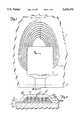
- FIG. 1is a top view of a thin film head and coil on a surface of a substrate.
- FIG. 2is a section view of the head shown in FIG. 1, taken at line 2--2 in FIG. 1.
- FIG. 3Ais a top view of a typical thin film head.
- FIGS. 3B and 3Cillustrate a process for ion-milling the magnetic pole for the head illustrated in FIG. 3A.
- FIGS. 4A-4Fillustrate the process of forming a diamond-like carbon mask in accordance with the presently preferred embodiment of the preferred invention.
- FIGS. 5A-5Dillustrate a modification of the process illustrated in FIGS. 4A-4F.
- FIGS. 1 and 2illustrate a thin film head having a pole piece ion-milled in accordance with either the process of the present invention, or that of the prior art.
- the resulting head structureis intended to be identical regardless of which process is employed, although some discernable defects may be evident in heads produced in accordance with the prior art.
- the heademploys a substrate 10 onto which a thin film magnetic transducer 12 is formed.
- the transducerincludes a bottom pole 14 and a top pole 16 separated by a layer 18 of insulating material forming a gap at the air-bearing surface 20. Layers 14 and 16 abut each other at the back gap distal from air-bearing surface 20.
- the headis fabricated on substrate or wafer 10 and cut or diced at line 20 to form an air-bearing surface.
- Coil 22passes through the head and between poles 14 and 16. Successive layers of coil 22 are insulated from each other and from poles 14 and 16 by successive insulating layers 24a, 24b, and 24c. As shown particularly in FIG. 1, coil 22 terminates at terminals 26 for connection to the read/write circuits of the disc drive. Also as shown in FIG. 2, a "hill" 28 is formed by the coil region 22 where the thickness of head 12 is greater than at the air-bearing surface 20. Hill 28 forms the transition between the two elevations.
- FIG. 3Aillustrates a typical thin film head prior to having been cut at line 20 to form the air-bearing surface.
- the hillis located generally at reference numeral 28.
- FIG. 3Bis a section view of the head 12 taken at line 3B--3B in FIG. 3A, illustrating a mask for ion-milling the shape of the top pole of head 12.
- the section view of FIG. 3Bis taken along the shoulder, and not through the active region of the head.
- the bottom pole 14 and insulator layer 18may be of the same shape as the top pole or may be larger, as shown. In either case, the principles of ion-milling the top pole are the same.
- a mask layer 30has been applied to the top surface 17 of top pole 16.
- Mask 30has been patterned, as at 32, in the shape shown in FIG. 3A, to expose magnetic material of top pole 16.
- pole 16 exposed by pattern 32 in mask 30it is the material of pole 16 exposed by pattern 32 in mask 30 that is to be ion-milled away.
- FIG. 3Cwhich is also taken along line 3B--3B in FIG. 3A, a void 34, corresponding to the region outside of the shoulder 13 of pole 16, is formed by the ion-milling process.
- both the mask 30 and the exposed portions of the magnetic material of layer 16are milled away by ion milling process.
- mask 30be of such thickness, and of such material, that the mask is not completely milled away before completion of milling of the pole.
- the photoresist maskwas applied by a spin-coating technique in which the material of the mask was applied to the surface of a wafer containing head 12 being produced and the wafer was spun to spread out the coating of mask material over the surface.
- the spreading of the materialis not altogether even, particularly at the region of the hills, where the material becomes thinner than in other regions.
- metal maskswhich are deposited rather than spin-coated, overcome the problems associated with spin coating, metal masks are patterned using etchants that also attack the magnetic pole being formed, making the process difficult to accurately control.
- Photoresisthas a mill rate approximately the same as an iron/nickel magnetic material.
- Metal maskswhen milled, typically have mill rates about one-half that of iron/nickel magnetic material. With a 50 percent safety factor, the thickness of a photoresist mask would be about 1.5 times the thickness of the magnetic material being milled, whereas a metal mask would have a thickness of about two-thirds the thickness of the corresponding magnetic material. In the case of photoresist, there some loss of control at the hill region 28. In the case of metal masks, great precision is required to prevent damage to the pole when patterning the mask.
- the present inventionis directed to the use of a diamond-like carbon mask in place of a photoresist or metal mask for use in ion-milling. More particularly, the present invention deals with the formation of a patterned diamond-like carbon mask on the top pole piece of a thin film magnetic head.
- the diamond-like carbonis advantageous over photoresist in that diamond-like carbon is deposited onto the wafer, rather than applied by a spin coating process.
- the diamond-like carbonis advantageous over metal masks in that diamond-like carbon is etched with oxygen etchants that do not attack the other layers of the head.
- the diamond-like carbonis patterned using a photoresist.
- mere substitution of diamond-like carbon for metalis not possible because the photoresist used to pattern the diamond-like carbon is subject to attack by the oxygen etchant employed to etch the diamond-like carbon.
- the process according to the present inventionis illustrated in FIGS. 4A-4F.
- magnetic head 12is shown with a bottom pole 14, top pole 16, and insulating gap layer 18.
- Coils 22forms the "hill" 28 between coils 22 and air-bearing surface 20.
- the formation of the mask on the top surface of pole 16is accomplished first by applying a layer 36 of diamond-like carbon to the top (exposed) surface of pole 16.
- a layer 38 of photoresistis applied over the layer 36 of diamond-like carbon and a layer 40 of insulating material, such as silicon dioxide (SiO 2 ), is applied over layer 38.
- layer 42 of photoresistis applied over layer 40.
- layer 42is patterned to the shape of the desired pole piece (such as shown in FIG. 3A).
- Patterning layer 42is usually accomplished by exposing the photoresist to light through a photomask and washing away the exposed portions of the mask at 44, leaving a portion of layer 40 exposed.
- a fluoride etchantsuch as CF 4 , is applied to the exposed portions of layer 40 to remove the silicon dioxide at 46 exposed by the photoresist layer 42, thereby exposing photoresist layer 38, as shown in FIG. 4C. That much of photoresist layer 40 exposed through opening 46 and all of the remainder of photoresist layer 42 are exposed to light, and washed away, as shown in FIG. 4D.
- the diamond-like carbon layer 36is exposed through exposed portion 48 of layer 38 in the pattern of the desired pole piece, with protected regions of the pole still being covered by photoresist 38 and silicon dioxide layer 40.
- the fluoride etchant used to etch the silicon dioxidewill not attack the diamond-like carbon layer 36.
- an anisotropic oxygen etchantis applied to the exposed portions of layer 36 to thereby expose the high moment magnetic layer 16 (FIG. 4E) through removed portion 50 in diamond-like carbon layer 36.
- the remainder of photoresist layer 38is dissolved, carrying away with it the remainder of the silicon dioxide layer 40, thereby leaving mask 36 patterned at 50, as shown in FIG. 4F.
- the structuremay now be ion milled as described in connection with FIGS. 3B and 3C to ion mill layer 16 to the pattern of mask 36 to achieve the desired pole piece.
- Diamond-like carbonis commercially known as "DLC" and is commercially available from a variety of sources.
- the diamond-like carbonis similar to diamond in physical properties.
- the materialis a hydrogenated carbon typically having a hydrogen content between about 30 to 50 percent and a large fraction of sp 3 carbon-carbon bonds rather than sp 2 found in ordinary graphite.
- the materialis typically formed from a hydrogenated carbon feedstock, such as methane (CH 4 ), processed by any of a variety of processes, such as an ion beam deposition process. It is theorized that during formation of diamond-like carbon, hydrogen is removed from the feedstock material forming a network of sp 3 bonded carbon atoms, rather than an ordered array of sp 2 bonded carbon, i.e. graphite.
- the materialresembles a hard, highly cross-linked polymer and exhibits a higher thermal conductivity than common electrical insulating material (such as SiO 2 or Al 2 O 3 ) and a high electrical resistivity, of the order of about 10 10 ⁇ -cm.
- Diamond-like carbon filmsare similar to diamonds in that they exhibit very high hardness ranges (1,000 to 5,000 on the Vickers hardness scale), a low coefficient of friction (of the order of less than 0.1) and densities between about 1.7 and 2.2.
- the materialis commercially referred to as "diamond-like" because of its similarity in characteristics to natural and synthetic diamond.
- the diamond-like carbonexhibits a high resistivity.
- An advantage of the diamond-like carbon maskis that the mask may be removed with an oxygen etchant without affecting the magnetic layer or other parts of the fabricated head.
- Table 1compares the relative mill rate for each of an iron/nickel magnetic material, photoresist, metal and diamond-like carbon (DLC).
- the mill rate for magnetic materialis about the same as a photoresist, twice as fast as metal, and about five times that of diamond-like carbon.
- the thickness of a photoresist maskshould be about 4.5 microns
- a thickness of a metal maskshould be about 2.25 microns
- a thickness of a diamond-like carbon maskshould be about 0.9 microns.
- diamond-like carbon layer 36has a thickness of about 0.9 microns for a 3 micron thick top pole 16, or about 30% of the thickness of the pole.
- FIGS. 4A-4FOne problem associated with the process illustrated in FIGS. 4A-4F is that if the etch rate of the diamond-like carbon is too slow, some undercutting of photoresist layer 38 may occur during the oxygen etchant step. For example, and with reference to FIGS. 4D and 4E, if, as the diamond-like carbon layer 36 is etched, some of the oxygen etchant attacks the photoresist layer 38, there may be some undercutting of the photoresist layer. If this occurs, additional carbon-like layer 36 is exposed to the oxygen etchant, which could affect the feature lines of the mask being produced. While this problem is usually avoided using an anisotropic oxygen etchant to provide very straight side walls, FIGS. 5A-5D illustrate a modification of the process illustrated in FIGS. 4A-4F to overcome this problem.
- Insulating layer 37is a protective layer, preferably formed of silicon dioxide having a thickness of at least about 0.5 microns. One-half micron is considered minimal to overcome the pin hole effects of SiO 2 .
- FIG. 5Bthe process is essentially identical to that described in connection with FIGS. 4B, 4C, and 4D, except that when the silicon dioxide layer 37 is exposed, the silicon dioxide layer 37 is etched with a fluoride etchant, such as CF 4 , and the exposed diamond-like carbon layer 36 is then etched with anisotropic oxygen etchant, as shown in FIG. 5C. The result, shown in FIG.
- FIG. 5Dcomprising a bilayer mask of diamond-like carbon layer 36 over pole 16 and capped with silicon dioxide layer 37.
- Layer 37protects layer 36 from oxygen etchant in the event that photoresist layer 38 is undercut by the oxygen etchant during the etching of layer 36.
- the resulting mask and structure shown in FIG. 5Dis used as described in FIGS. 3B and 3C in an ion milling process to shape the top pole 16.
- SiO 2has an ion mill rate higher than Ni/Fe.
- the effect of layer 37 on the overall mill timeis slight, although for an Ni/Fe pole thickness of 3 microns, the thickness of layer 36 of diamond-like material may be reduced to about 25% of the thickness of the pole, or about 0.8 microns for a 3 microns thick pole.
- One feature of the inventionis the fact that the diamond-like carbon is applied by an ion beam deposition directly onto layer 16.
- the simplicity of the ion beam processpermits the formation of low defect films in the form of mask 36.
- Other techniques for applying the diamond-like carbon to layer 16include radio frequency and direct current magnetron sputtering, carbon-arc deposition, laser ablation, and plasma enhanced chemical vapor deposition (PECVD).
Landscapes
- Chemical & Material Sciences (AREA)
- Engineering & Computer Science (AREA)
- Materials Engineering (AREA)
- Mechanical Engineering (AREA)
- Metallurgy (AREA)
- Organic Chemistry (AREA)
- Manufacturing & Machinery (AREA)
- Magnetic Heads (AREA)
Abstract
Description
TABLE I______________________________________ Fe/Ni Resist Metal DLC______________________________________Relative Mill Rate 5 5 2.5 1Mask Thickness (μm) 4.5 2.25 0.9______________________________________
Claims (13)
Priority Applications (1)
| Application Number | Priority Date | Filing Date | Title |
|---|---|---|---|
| US08/571,395US5658470A (en) | 1995-12-13 | 1995-12-13 | Diamond-like carbon for ion milling magnetic material |
Applications Claiming Priority (1)
| Application Number | Priority Date | Filing Date | Title |
|---|---|---|---|
| US08/571,395US5658470A (en) | 1995-12-13 | 1995-12-13 | Diamond-like carbon for ion milling magnetic material |
Publications (1)
| Publication Number | Publication Date |
|---|---|
| US5658470Atrue US5658470A (en) | 1997-08-19 |
Family
ID=24283537
Family Applications (1)
| Application Number | Title | Priority Date | Filing Date |
|---|---|---|---|
| US08/571,395Expired - Fee RelatedUS5658470A (en) | 1995-12-13 | 1995-12-13 | Diamond-like carbon for ion milling magnetic material |
Country Status (1)
| Country | Link |
|---|---|
| US (1) | US5658470A (en) |
Cited By (16)
| Publication number | Priority date | Publication date | Assignee | Title |
|---|---|---|---|---|
| US6400527B1 (en) | 1998-11-13 | 2002-06-04 | Alps Electric Co., Ltd. | Thin film magnetic head having upper core layer with narrow track width |
| US6569580B2 (en) | 2001-03-13 | 2003-05-27 | Diverging Technologies, Inc. | Binary and phase-shift photomasks |
| US20040264046A1 (en)* | 2003-06-25 | 2004-12-30 | Hitachi Global Storage Technologies | Magnetic head with thinned T-shaped write pole and its fabrication |
| US6846985B2 (en) | 2002-01-22 | 2005-01-25 | Nanoset, Llc | Magnetically shielded assembly |
| US6859997B1 (en) | 2000-09-19 | 2005-03-01 | Western Digital (Fremont), Inc. | Method for manufacturing a magnetic write element |
| US20050068665A1 (en)* | 2003-09-26 | 2005-03-31 | Hitachi Global Storage Technologies | Write pole fabrication for perpendicular recording |
| US20050091266A1 (en)* | 2003-10-23 | 2005-04-28 | Fujitsu Limited | Data file system, data access server and data access program storage medium |
| US20050127030A1 (en)* | 2003-07-24 | 2005-06-16 | Fuji Xerox Co., Ltd. | Carbon nanotube structure, method of manufacturing the same, carbon nanotube transfer body, and liquid solution |
| US20050201011A1 (en)* | 2004-03-10 | 2005-09-15 | Hitachi Global Storage Technologies, Inc. | Planarized perpendicular pole tip system and method for manufacturing the same |
| US20060021579A1 (en)* | 2004-07-30 | 2006-02-02 | Bernaski Ryan R | Non-stick masking fixtures and methods of preparing same |
| US20060156537A1 (en)* | 2005-01-18 | 2006-07-20 | Druist David P | Method for protecting write head coil during write pole notching using ion mill resistant mask formed by reactive ion etching |
| US7139153B2 (en) | 2004-02-23 | 2006-11-21 | Hitachi Global Storage Technologies Netherlands B.V. | Magnetic pole tip for perpendicular magnetic recording |
| US7162302B2 (en) | 2002-03-04 | 2007-01-09 | Nanoset Llc | Magnetically shielded assembly |
| US7473843B2 (en) | 2002-01-22 | 2009-01-06 | Biophan Technologies, Inc. | Magnetic resonance imaging coated assembly |
| US8091210B1 (en) | 2008-03-05 | 2012-01-10 | Western Digital (Fremont), Llc | Method for providing a structure in magnetic recording transducer |
| US20130004763A1 (en)* | 2011-06-30 | 2013-01-03 | Seagate Technology, Llc | Method of patterning a stack |
Citations (15)
| Publication number | Priority date | Publication date | Assignee | Title |
|---|---|---|---|---|
| US4052749A (en)* | 1976-05-19 | 1977-10-04 | Matsushita Electric Industrial Co., Ltd. | Thin film magnetic head |
| GB2064849A (en)* | 1979-11-28 | 1981-06-17 | Philips Nv | Integrated magnetic transducer head |
| JPS59210520A (en)* | 1983-05-14 | 1984-11-29 | Yukio Ichinose | Magnetic head |
| JPS61216109A (en)* | 1985-03-20 | 1986-09-25 | Matsushita Electric Ind Co Ltd | Thin film magnetic head |
| JPS61242313A (en)* | 1985-04-19 | 1986-10-28 | Hitachi Ltd | Magnetoresistive thin film head |
| JPS6233317A (en)* | 1985-08-06 | 1987-02-13 | Matsushita Electric Ind Co Ltd | Thin film magnetic head |
| JPS644913A (en)* | 1987-06-26 | 1989-01-10 | Kansai Nippon Electric | Thin film magnetic head |
| US5087608A (en)* | 1989-12-28 | 1992-02-11 | Bell Communications Research, Inc. | Environmental protection and patterning of superconducting perovskites |
| JPH04147411A (en)* | 1990-10-09 | 1992-05-20 | Mitsubishi Electric Corp | Manufacturing method of thin film magnetic head |
| EP0493902A2 (en)* | 1990-12-27 | 1992-07-08 | International Business Machines Corporation | Magnetic head slider and method for making same |
| US5271802A (en)* | 1990-12-27 | 1993-12-21 | International Business Machines Corporation | Method for making a thin film magnetic head having a protective coating |
| EP0584707A2 (en)* | 1992-08-21 | 1994-03-02 | Minnesota Mining And Manufacturing Company | Laminate and wear-resistant thin-film magnetic head assembly formed thereon |
| US5363265A (en)* | 1991-09-17 | 1994-11-08 | Seagate Technology, Inc. | Planarized magnetoresistive sensor |
| US5378316A (en)* | 1991-04-03 | 1995-01-03 | Eastman Kodak Company | High durability mask for dry etch processing of GaAs |
| WO1995018442A1 (en)* | 1993-12-30 | 1995-07-06 | Seagate Technology, Inc. | Amorphous diamond-like carbon gaps in magnetoresistive heads |
- 1995
- 1995-12-13USUS08/571,395patent/US5658470A/ennot_activeExpired - Fee Related
Patent Citations (15)
| Publication number | Priority date | Publication date | Assignee | Title |
|---|---|---|---|---|
| US4052749A (en)* | 1976-05-19 | 1977-10-04 | Matsushita Electric Industrial Co., Ltd. | Thin film magnetic head |
| GB2064849A (en)* | 1979-11-28 | 1981-06-17 | Philips Nv | Integrated magnetic transducer head |
| JPS59210520A (en)* | 1983-05-14 | 1984-11-29 | Yukio Ichinose | Magnetic head |
| JPS61216109A (en)* | 1985-03-20 | 1986-09-25 | Matsushita Electric Ind Co Ltd | Thin film magnetic head |
| JPS61242313A (en)* | 1985-04-19 | 1986-10-28 | Hitachi Ltd | Magnetoresistive thin film head |
| JPS6233317A (en)* | 1985-08-06 | 1987-02-13 | Matsushita Electric Ind Co Ltd | Thin film magnetic head |
| JPS644913A (en)* | 1987-06-26 | 1989-01-10 | Kansai Nippon Electric | Thin film magnetic head |
| US5087608A (en)* | 1989-12-28 | 1992-02-11 | Bell Communications Research, Inc. | Environmental protection and patterning of superconducting perovskites |
| JPH04147411A (en)* | 1990-10-09 | 1992-05-20 | Mitsubishi Electric Corp | Manufacturing method of thin film magnetic head |
| EP0493902A2 (en)* | 1990-12-27 | 1992-07-08 | International Business Machines Corporation | Magnetic head slider and method for making same |
| US5271802A (en)* | 1990-12-27 | 1993-12-21 | International Business Machines Corporation | Method for making a thin film magnetic head having a protective coating |
| US5378316A (en)* | 1991-04-03 | 1995-01-03 | Eastman Kodak Company | High durability mask for dry etch processing of GaAs |
| US5363265A (en)* | 1991-09-17 | 1994-11-08 | Seagate Technology, Inc. | Planarized magnetoresistive sensor |
| EP0584707A2 (en)* | 1992-08-21 | 1994-03-02 | Minnesota Mining And Manufacturing Company | Laminate and wear-resistant thin-film magnetic head assembly formed thereon |
| WO1995018442A1 (en)* | 1993-12-30 | 1995-07-06 | Seagate Technology, Inc. | Amorphous diamond-like carbon gaps in magnetoresistive heads |
Non-Patent Citations (16)
| Title |
|---|
| IBM Technical Disclosure Bulletin, vol. 31, No. 12, May 1989, Armonk, N.Y., US, pp. 317 318. Low Stress Dielectric Coatings for Copper Parts .* |
| IBM Technical Disclosure Bulletin, vol. 31, No. 12, May 1989, Armonk, N.Y., US, pp. 317-318. "Low Stress Dielectric Coatings for Copper Parts". |
| IBM Technical Disclosure Bulletin, vol. 34, No. 2, Jul. 1991, Armonk, N.Y., US, pp. 19 20, Thermal Ink Jet Heater Devices Incorporating Diamond Like Carbon Films As Protective Overcoats .* |
| IBM Technical Disclosure Bulletin, vol. 34, No. 2, Jul. 1991, Armonk, N.Y., US, pp. 19-20, "Thermal Ink Jet Heater Devices Incorporating Diamond-Like Carbon Films As Protective Overcoats". |
| Patent Abstracts of Japan, vol. 11, No. 211 (P 594) 9 Jul. 1987 & JP,A,62 033 317 (Matsushita Electric Ind Co Ltd) 13 Feb. 1987.* |
| Patent Abstracts of Japan, vol. 11, No. 211 (P-594) 9 Jul. 1987 & JP,A,62 033 317 (Matsushita Electric Ind Co Ltd) 13 Feb. 1987. |
| Patent Abstracts of Japan, vol. 11, No. 49 (P 547) 14 Feb. 1987 & JP,A,61 216 109 (Matsushita Electric Ind Co Ltd) 25 Sep. 1986.* |
| Patent Abstracts of Japan, vol. 11, No. 49 (P-547) 14 Feb. 1987 & JP,A,61 216 109 (Matsushita Electric Ind Co Ltd) 25 Sep. 1986. |
| Patent Abstracts of Japan, vol. 11, No. 91 (P 558) (2538) 23 Mar. 1987 & JP,A,61 242 313 (Hitachi Ltd) 28 Oct. 1986.* |
| Patent Abstracts of Japan, vol. 11, No. 91 (P-558) (2538) 23 Mar. 1987 & JP,A,61 242 313 (Hitachi Ltd) 28 Oct. 1986. |
| Patent Abstracts of Japan, vol. 13, No. 167 (P 861) 20 Apr. 1989 & JP,A,01 004 913 (NEC Kansai Ltd) 10 Jan. 1989.* |
| Patent Abstracts of Japan, vol. 13, No. 167 (P-861) 20 Apr. 1989 & JP,A,01 004 913 (NEC Kansai Ltd) 10 Jan. 1989. |
| Patent Abstracts of Japan, vol. 16, No. 430 (P 1417) 9 Sep. 1992 & JP,A,04 147 411 (Mitsubishi Electric Corp) 20 May 1992.* |
| Patent Abstracts of Japan, vol. 16, No. 430 (P-1417) 9 Sep. 1992 & JP,A,04 147 411 (Mitsubishi Electric Corp) 20 May 1992. |
| Patent Abstracts of Japan, vol. 9, No. 79 (P 347) (1802) 9 Apr. 1985 & JP,A,59 210 520 (Yukio Ichinose) 29 Nov. 1984.* |
| Patent Abstracts of Japan, vol. 9, No. 79 (P-347) (1802) 9 Apr. 1985 & JP,A,59 210 520 (Yukio Ichinose) 29 Nov. 1984. |
Cited By (24)
| Publication number | Priority date | Publication date | Assignee | Title |
|---|---|---|---|---|
| US6400527B1 (en) | 1998-11-13 | 2002-06-04 | Alps Electric Co., Ltd. | Thin film magnetic head having upper core layer with narrow track width |
| US6859997B1 (en) | 2000-09-19 | 2005-03-01 | Western Digital (Fremont), Inc. | Method for manufacturing a magnetic write element |
| US6569580B2 (en) | 2001-03-13 | 2003-05-27 | Diverging Technologies, Inc. | Binary and phase-shift photomasks |
| US6846985B2 (en) | 2002-01-22 | 2005-01-25 | Nanoset, Llc | Magnetically shielded assembly |
| US7473843B2 (en) | 2002-01-22 | 2009-01-06 | Biophan Technologies, Inc. | Magnetic resonance imaging coated assembly |
| US7162302B2 (en) | 2002-03-04 | 2007-01-09 | Nanoset Llc | Magnetically shielded assembly |
| US7092206B2 (en) | 2003-06-25 | 2006-08-15 | Hitachi Global Storage Technologies Netherlands B.V. | Magnetic head with magnetic layers of differing widths and third pole with reduced thickness |
| US20040264046A1 (en)* | 2003-06-25 | 2004-12-30 | Hitachi Global Storage Technologies | Magnetic head with thinned T-shaped write pole and its fabrication |
| US20050127030A1 (en)* | 2003-07-24 | 2005-06-16 | Fuji Xerox Co., Ltd. | Carbon nanotube structure, method of manufacturing the same, carbon nanotube transfer body, and liquid solution |
| US20050068665A1 (en)* | 2003-09-26 | 2005-03-31 | Hitachi Global Storage Technologies | Write pole fabrication for perpendicular recording |
| US7120988B2 (en) | 2003-09-26 | 2006-10-17 | Hitachi Global Storage Technologies Netherlands B.V. | Method for forming a write head having air bearing surface (ABS) |
| US20050091266A1 (en)* | 2003-10-23 | 2005-04-28 | Fujitsu Limited | Data file system, data access server and data access program storage medium |
| US7139153B2 (en) | 2004-02-23 | 2006-11-21 | Hitachi Global Storage Technologies Netherlands B.V. | Magnetic pole tip for perpendicular magnetic recording |
| US7248434B2 (en) | 2004-03-10 | 2007-07-24 | Hitachi Global Storage Technologies Netherlands B.V. | Planarized perpendicular pole tip system and method for manufacturing the same |
| US20050201011A1 (en)* | 2004-03-10 | 2005-09-15 | Hitachi Global Storage Technologies, Inc. | Planarized perpendicular pole tip system and method for manufacturing the same |
| US20060021579A1 (en)* | 2004-07-30 | 2006-02-02 | Bernaski Ryan R | Non-stick masking fixtures and methods of preparing same |
| US8349086B2 (en)* | 2004-07-30 | 2013-01-08 | United Technologies Corporation | Non-stick masking fixtures and methods of preparing same |
| US8603582B2 (en) | 2004-07-30 | 2013-12-10 | United Technologies Corporation | Non-stick masking fixtures and methods of preparing same |
| US20060156537A1 (en)* | 2005-01-18 | 2006-07-20 | Druist David P | Method for protecting write head coil during write pole notching using ion mill resistant mask formed by reactive ion etching |
| US7243411B2 (en)* | 2005-01-18 | 2007-07-17 | Hitachi Global Storage Technologies Netherlands B.V. | Method for protecting write head coil during write pole/shaping |
| US8091210B1 (en) | 2008-03-05 | 2012-01-10 | Western Digital (Fremont), Llc | Method for providing a structure in magnetic recording transducer |
| US20130004763A1 (en)* | 2011-06-30 | 2013-01-03 | Seagate Technology, Llc | Method of patterning a stack |
| US9284649B2 (en)* | 2011-06-30 | 2016-03-15 | Seagate Technology Llc | Method of patterning a stack |
| US9809887B2 (en) | 2011-06-30 | 2017-11-07 | Seagate Technology Llc | Method of patterning a stack |
Similar Documents
| Publication | Publication Date | Title |
|---|---|---|
| US5658470A (en) | Diamond-like carbon for ion milling magnetic material | |
| US4878290A (en) | Method for making thin film magnetic head | |
| US4652954A (en) | Method for making a thin film magnetic head | |
| US5681426A (en) | Diamond-like carbon wet etchant stop for formation of magnetic transducers | |
| US6282776B1 (en) | Magnetic head and method of manufacturing the same | |
| KR0147976B1 (en) | Pattern flattening method of thin film head | |
| JPS6142714A (en) | Manufacture of multilayer conductor film structure | |
| US5718949A (en) | Diamond-like carbon encapsulation of magnetic heads | |
| US6067703A (en) | Method for fabricating a combined thin film magnetic head | |
| US20020186503A1 (en) | Metal in gap thin film tape head | |
| JP2702215B2 (en) | Method for manufacturing thin-film magnetic head | |
| KR0147996B1 (en) | A method for planarization patterning onto a thin film head | |
| JP3366582B2 (en) | Thin film magnetic head and method of manufacturing the same | |
| KR100263546B1 (en) | Method of manufacturing thin film magnetic head | |
| JPH0644528A (en) | Thin-film magnetic head and its production | |
| JPS59168913A (en) | Gap forming method of thin film magnetic head | |
| JPS62170011A (en) | Manufacture of thin film magnetic head | |
| KR100256065B1 (en) | Method of manufacturing thin film magnetic head | |
| JP2605535B2 (en) | Method for manufacturing thin-film magnetic head | |
| KR100289181B1 (en) | Manufacturing method of magnetoresistive head | |
| JPH02247808A (en) | Thin film magnetic head and its production | |
| JPH05274626A (en) | Mr head | |
| JPS63257910A (en) | Thin film magnetic head | |
| JPH04281204A (en) | Etching method | |
| KR980004379A (en) | Thin film magnetic head manufacturing method |
Legal Events
| Date | Code | Title | Description |
|---|---|---|---|
| CC | Certificate of correction | ||
| AS | Assignment | Owner name:SEAGATE TECHNOLOGY LLC, CALIFORNIA Free format text:ASSIGNMENT OF ASSIGNORS INTEREST;ASSIGNOR:SEAGATE TECHNOLOGY, INC.;REEL/FRAME:011077/0319 Effective date:20000728 | |
| FPAY | Fee payment | Year of fee payment:4 | |
| AS | Assignment | Owner name:THE CHASE MANHATTAN BANK, AS COLLATERAL AGENT, NEW Free format text:SECURITY AGREEMENT;ASSIGNOR:SEAGATE TECHNOLOGY LLC;REEL/FRAME:011461/0001 Effective date:20001122 | |
| AS | Assignment | Owner name:JPMORGAN CHASE BANK, AS COLLATERAL AGENT, NEW YORK Free format text:SECURITY AGREEMENT;ASSIGNOR:SEAGATE TECHNOLOGY LLC;REEL/FRAME:013177/0001 Effective date:20020513 Owner name:JPMORGAN CHASE BANK, AS COLLATERAL AGENT,NEW YORK Free format text:SECURITY AGREEMENT;ASSIGNOR:SEAGATE TECHNOLOGY LLC;REEL/FRAME:013177/0001 Effective date:20020513 | |
| REMI | Maintenance fee reminder mailed | ||
| LAPS | Lapse for failure to pay maintenance fees | ||
| STCH | Information on status: patent discontinuation | Free format text:PATENT EXPIRED DUE TO NONPAYMENT OF MAINTENANCE FEES UNDER 37 CFR 1.362 | |
| FP | Lapsed due to failure to pay maintenance fee | Effective date:20050819 | |
| AS | Assignment | Owner name:SEAGATE TECHNOLOGY LLC, CALIFORNIA Free format text:RELEASE OF SECURITY INTERESTS IN PATENT RIGHTS;ASSIGNOR:JPMORGAN CHASE BANK, N.A. (FORMERLY KNOWN AS THE CHASE MANHATTAN BANK AND JPMORGAN CHASE BANK), AS ADMINISTRATIVE AGENT;REEL/FRAME:016937/0554 Effective date:20051130 |