US5656844A - Semiconductor-on-insulator transistor having a doping profile for fully-depleted operation - Google Patents
Semiconductor-on-insulator transistor having a doping profile for fully-depleted operationDownload PDFInfo
- Publication number
- US5656844A US5656844AUS08/507,898US50789895AUS5656844AUS 5656844 AUS5656844 AUS 5656844AUS 50789895 AUS50789895 AUS 50789895AUS 5656844 AUS5656844 AUS 5656844A
- Authority
- US
- United States
- Prior art keywords
- transistor
- dopant concentration
- insulating layer
- channel region
- top surface
- Prior art date
- Legal status (The legal status is an assumption and is not a legal conclusion. Google has not performed a legal analysis and makes no representation as to the accuracy of the status listed.)
- Expired - Lifetime
Links
Images

Classifications
- H—ELECTRICITY
- H10—SEMICONDUCTOR DEVICES; ELECTRIC SOLID-STATE DEVICES NOT OTHERWISE PROVIDED FOR
- H10D—INORGANIC ELECTRIC SEMICONDUCTOR DEVICES
- H10D30/00—Field-effect transistors [FET]
- H10D30/01—Manufacture or treatment
- H10D30/021—Manufacture or treatment of FETs having insulated gates [IGFET]
- H10D30/031—Manufacture or treatment of FETs having insulated gates [IGFET] of thin-film transistors [TFT]
- H10D30/0321—Manufacture or treatment of FETs having insulated gates [IGFET] of thin-film transistors [TFT] comprising silicon, e.g. amorphous silicon or polysilicon
- H10D30/0323—Manufacture or treatment of FETs having insulated gates [IGFET] of thin-film transistors [TFT] comprising silicon, e.g. amorphous silicon or polysilicon comprising monocrystalline silicon
- H—ELECTRICITY
- H10—SEMICONDUCTOR DEVICES; ELECTRIC SOLID-STATE DEVICES NOT OTHERWISE PROVIDED FOR
- H10D—INORGANIC ELECTRIC SEMICONDUCTOR DEVICES
- H10D30/00—Field-effect transistors [FET]
- H10D30/60—Insulated-gate field-effect transistors [IGFET]
- H10D30/67—Thin-film transistors [TFT]
- H10D30/6704—Thin-film transistors [TFT] having supplementary regions or layers in the thin films or in the insulated bulk substrates for controlling properties of the device
- H10D30/6708—Thin-film transistors [TFT] having supplementary regions or layers in the thin films or in the insulated bulk substrates for controlling properties of the device for preventing the kink effect or the snapback effect, e.g. discharging the minority carriers of the channel region for preventing bipolar effect
- H—ELECTRICITY
- H10—SEMICONDUCTOR DEVICES; ELECTRIC SOLID-STATE DEVICES NOT OTHERWISE PROVIDED FOR
- H10D—INORGANIC ELECTRIC SEMICONDUCTOR DEVICES
- H10D30/00—Field-effect transistors [FET]
- H10D30/60—Insulated-gate field-effect transistors [IGFET]
- H10D30/67—Thin-film transistors [TFT]
- H10D30/6757—Thin-film transistors [TFT] characterised by the structure of the channel, e.g. transverse or longitudinal shape or doping profile
- H—ELECTRICITY
- H10—SEMICONDUCTOR DEVICES; ELECTRIC SOLID-STATE DEVICES NOT OTHERWISE PROVIDED FOR
- H10D—INORGANIC ELECTRIC SEMICONDUCTOR DEVICES
- H10D30/00—Field-effect transistors [FET]
- H10D30/60—Insulated-gate field-effect transistors [IGFET]
- H10D30/67—Thin-film transistors [TFT]
- H10D30/6758—Thin-film transistors [TFT] characterised by the insulating substrates
- H10D30/6759—Silicon-on-sapphire [SOS] substrates
Definitions
- the present inventionrelates, in general, to semiconductor devices and, more particularly, to semiconductor-on-insulator devices operating in a fully-depleted mode.
- SOI devicesare typically formed using silicon and generally operate in either a partially-depleted mode or a fully-depleted mode.
- SOI devices operating in a fully-depleted modeexhibit very low sub-threshold slope and do not suffer from the so-called kink effect, however, such devices have a large threshold voltage sensitivity to the thickness of the thin-silicon film used for manufacture (for example, this sensitivity is typically 100 mV/100 angstroms), and require thin silicon films having a thickness of about 800 angstroms.
- this sensitivityis typically 100 mV/100 angstroms
- thin silicon films having a thickness of about 800 angstromsare significant because such a thin silicon film is difficult to manufacture with uniformity.
- the large threshold voltage sensitivityleads to non-uniform threshold voltages for the manufactured devices.
- SOI devices operating in a partially-depleted modehave reduced threshold voltage sensitivity to the thickness of the thin silicon film and are easier to manufacture because the thickness of the thin film can be greater than that required for fully-depleted devices.
- partially-depleted devicesexhibit the kink effect, which adversely affects their use in analog applications. They also exhibit a degradation of sub-threshold slope compared to devices operating in the fully-depleted mode. A degraded sub-threshold slope increases device leakage when the device is turned "off".
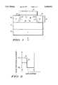
- FIG. 1is a cross-sectional view of a semiconductor-on-insulator transistor according to the present invention
- FIG. 2is a graph illustrating dopant concentration versus depth for the channel region of the transistor of FIG. 1 according to a first embodiment of the present invention.
- FIG. 3is a graph illustrating dopant concentration versus depth for the channel region of the transistor of FIG. 1 according to a second embodiment.
- the present inventionprovides a semiconductor-on-insulator (SOI) transistor with a non-uniformly doped channel region.
- SOIsemiconductor-on-insulator
- the non-uniformity of the channel doping profileprovides a transistor that operates in a fully-depleted mode and has a reasonable threshold voltage, yet that can be formed using significantly thicker semiconductor films than with prior SOI devices.
- the transistoralso has significantly reduced threshold voltage sensitivity to the thickness of the semiconductor film.
- FIG. 1illustrates a cross-section of a semiconductor-on-insulator transistor 10 according to the present invention.
- Transistor 10is generally conventional in structure and has a buried insulating layer 12 on a semiconductor substrate 14.
- Substrate 14is preferably silicon, and insulating layer 12 is, for example, silicon oxide having a thickness of about 2,000-10,000 angstroms. Sapphire can also be used for insulating layer 12.
- a semiconductor film 16 of, for example, siliconhas been formed on insulating layer 12 using well-known techniques.
- Film 16is preferably silicon, and generally has a thickness of about 800-2,000 angstroms, and more preferably about 1,200-2,000 angstroms. Also, in some cases, film 16's thickness can be as low as about 500 angstroms.
- transistor 10will be operated in a fully-depleted mode, it should be noted that the thickness of film 16 can be greater than the 800 angstroms thickness required by prior fully-depleted devices as discussed below.
- a source region 18 and a drain region 20have been formed in film 16 using conventional methods including, for example, heavy doping with an N-type dopant.
- N-channel deviceis illustrated in FIG. 1 and described herein, one of skill in the art will recognize that the present invention can also be used with a P-channel device.
- Halo regions 22 and 24are also illustrated in FIG. 1, but are optional and preferably used to avoid the adverse short channel effects associated with drain-induced barrier lowering (DIBL). Halo regions 22 and 24 can be formed using well-known methods. As is known, halo regions 22 and 24 are doped with a dopant of an opposite conductivity type from that used to form source and drain regions 18 and 20.
- DIBLdrain-induced barrier lowering
- gate insulating layer 26 and a gate electrode layer 28have been formed on film 16 using conventional techniques.
- Gate insulating layer 26is preferably a silicon oxide layer having a thickness of, for example, about 50-150 angstroms
- gate electrode layer 28is, for example, a polysilicon layer having a thickness of, for example, about 3,000 angstroms.
- a channel region 30underlies gate insulating layer 26 and is bounded by a top surface 32 and a bottom surface 34 of film 16.
- channel region 30has a non-uniform doping profile that provides a significant change in dopant concentration across channel region 30 from top surface 32 to bottom surface 34. More specifically, for the case of an N-channel device, channel region 30 is lightly P-doped so that the dopant concentration at top surface 32 is significantly greater than the dopant concentration at bottom surface 34. This non-uniform doping profile is in sharp contrast to the uniformly-doped thin films considered desirable for use in prior SOI devices.
- FIG. 2illustrates an ideal doping profile for channel region 30 for a first embodiment of the present invention.
- the logarithm of the dopant concentration in channel region 30(log (atoms/cm 3 )) is plotted versus the vertical depth into the channel region 30 from top surface 32 as indicated by dashed line 36 in FIG. 1.
- a step distribution 38has an abrupt step 40 located a distance D vertically downward into channel region 30.
- the dopant concentration of channel region 30 at top surface 32is indicated in FIG. 2 by N T
- the dopant concentration at bottom surface 34is indicated by N B .
- the total thickness of channel region 30is indicated by T.
- the doping ratiois preferably greater than about 5, and more preferably between about 10 and 100.
- a doping ratio as low as about two or threeis still believed to provide some benefits.
- specific rangesare given here, one of skill in the art will recognize that it is the non-uniformity of the doping profile in channel region 30 that provides the advantages discussed below.
- the present inventionincludes any doping profile that is non-uniform and has N T >N B .
- Step distribution 38is a preferred, ideal distribution of dopant in channel region 30, and distribution 38 is preferably approximated to the extent practicable using conventional doping techniques and as limited by one's particular process integration.
- shallow, direct ion implantation techniqueswell-known to those skilled in the art can be used to roughly approximate step distribution 38.
- FIG. 3illustrates a doping profile for a second embodiment of the present invention corresponding to one particular doping technique.
- a doped region formed by conventional ion implantation and annealingtypically exhibits a gaussian-like distribution.
- the peak of the gaussian-like distributionis substantially centered in channel region 30 to provide a uniform profile.
- a gaussian-like curve 42is positioned so that the peak of the gaussian distribution corresponds substantially to N T , and the tail of the distribution corresponds to N B .
- gaussian-like curve 42can be positioned in this manner by ion implantation through device layers of an appropriate combined thickness that are overlying channel region 30 during the threshold voltage implantation step of the process sequence used to form transistor 10. These layers include, for example, gate insulating layer 26 and a precursor layer (not shown) to gate electrode layer 28 as discussed further below.
- depth Droughly corresponds to a point 44 of a maximal slope of gaussian-like curve 42.
- the particular depth D selected for either step 40 or point 44 and dopant concentrations N T and N Bare design choices that are selected as determined by the needs of a particular application, as is known to one of skill in the art.
- channel region 30typically has a doping profile that monotonically decreases from top surface 32 to bottom surface 34 of film 16.
- the doping profilemay not monotonically decrease as a result of the doping method used as discussed herein.
- the particular depth D for step 40 or point 44is not critical and is generally positioned, for example, about halfway between top surface 32 and bottom surface 34.
- dopant concentration N Tis selected to provide a threshold voltage for transistor 10 that is preferably greater than about 400 mV, but lower threshold voltages such as about 300 mV may be sufficient or desirable in certain applications. Generally, N T will be greater than about 8 ⁇ 10 16 atoms/cm 3 . As a specific example, when approximating the step profile illustrated in FIG. 2 for a depth D of about 800 angstroms and a film 16 thickness of about 1,800 angstroms, N T is about 1.2 ⁇ 10 17 atoms/cm 3 to provide a threshold voltage of about 400 mV, and N B is about 1.2 ⁇ 10 16 atoms/cm 3 to provide fully-depleted operation.
- gate insulating layer 26is silicon oxide with a thickness of about 105 angstroms
- gate electrode layer 28is polysilicon with a thickness of about 3,000 angstroms.
- the threshold voltageincreases.
- the channel integrated dopant concentrationis primarily controlled by dopant concentration N T at top surface 32 because dopant concentration N B at bottom surface 34 is made significantly less than N T , as discussed above.
- Transistor 10is generally manufactured using conventional techniques well-known to those of skill in the art. However, in one specific example, the doping of channel region 30 can be done by an ion implant through gate insulating layer 26 and gate electrode layer 28.
- gate electrode layer 28has a preferred final thickness of about 3,000 angstroms, in order to achieve an appropriate depth D, an ion implant is performed at a point in the processing sequence at which gate electrode layer 28, which is a precursor layer of preferably polysilicon or amorphous silicon, has a thickness of about 500 angstroms and gate insulating layer 26, which is preferably silicon oxide, has a thickness of about 100 angstroms.
- boronis ion implanted at a dose of about 1.0-2.0 ⁇ 10 12 atoms/cm 2 and an energy of about 15-20 keV
- phosphorusis implanted at a dose of about 1.5-2.5 ⁇ 10 12 atoms/cm 2 and an energy of about 45-55 keV.
- Film 16is preferably silicon having a thickness of about 1,500-2,000 angstroms.
- transistor 10In a later processing step, additional polysilicon is deposited on the precursor layer above to provide the final thickness of gate electrode layer 28.
- the remaining processing steps for transistor 10are done using well-known methods. It should be noted that when optional halo regions 22 and 24 are used in transistor 10, they have a dopant concentration greater than dopant concentration N B of channel region 30.
- the peak concentration of the doping profile in channel region 30may be positioned somewhat below, rather than at, top surface 32. Also, in some cases, the minimum concentration of the doping profile will be slightly above bottom surface 34. Such profiles are still considered to be within the scope of the present invention. It is sufficient in such cases that the doping profile be significantly non-uniform substantially as described above.
- the ratio of such a peak concentration to a minimum concentration of a vertical doping profile for channel region 30is also preferably about 5, and more preferably about 10-100, but some benefits are still observed where the ratio is only about two or three.
Landscapes
- Thin Film Transistor (AREA)
Abstract
Description
Claims (24)
Priority Applications (3)
| Application Number | Priority Date | Filing Date | Title |
|---|---|---|---|
| US08/507,898US5656844A (en) | 1995-07-27 | 1995-07-27 | Semiconductor-on-insulator transistor having a doping profile for fully-depleted operation |
| JP8213042AJPH0945919A (en) | 1995-07-27 | 1996-07-24 | Semiconductor-on-insulator transistor |
| KR1019960030529AKR970008332A (en) | 1995-07-27 | 1996-07-26 | SOI transistor with a full-depletion dynamic doping profile |
Applications Claiming Priority (1)
| Application Number | Priority Date | Filing Date | Title |
|---|---|---|---|
| US08/507,898US5656844A (en) | 1995-07-27 | 1995-07-27 | Semiconductor-on-insulator transistor having a doping profile for fully-depleted operation |
Publications (1)
| Publication Number | Publication Date |
|---|---|
| US5656844Atrue US5656844A (en) | 1997-08-12 |
Family
ID=24020582
Family Applications (1)
| Application Number | Title | Priority Date | Filing Date |
|---|---|---|---|
| US08/507,898Expired - LifetimeUS5656844A (en) | 1995-07-27 | 1995-07-27 | Semiconductor-on-insulator transistor having a doping profile for fully-depleted operation |
Country Status (3)
| Country | Link |
|---|---|
| US (1) | US5656844A (en) |
| JP (1) | JPH0945919A (en) |
| KR (1) | KR970008332A (en) |
Cited By (20)
| Publication number | Priority date | Publication date | Assignee | Title |
|---|---|---|---|---|
| US5821584A (en)* | 1995-12-06 | 1998-10-13 | Micron Technology, Inc. | Thin film transistors comprising drain offset regions |
| US5920093A (en)* | 1997-04-07 | 1999-07-06 | Motorola, Inc. | SOI FET having gate sub-regions conforming to t-shape |
| US5936278A (en)* | 1996-03-13 | 1999-08-10 | Texas Instruments Incorporated | Semiconductor on silicon (SOI) transistor with a halo implant |
| US5989963A (en)* | 1997-07-21 | 1999-11-23 | Advanced Micro Devices, Inc. | Method for obtaining a steep retrograde channel profile |
| US6245649B1 (en) | 1999-02-17 | 2001-06-12 | Advanced Micro Devices, Inc. | Method for forming a retrograde impurity profile |
| US6373103B1 (en) | 2000-03-31 | 2002-04-16 | Advanced Micro Devices, Inc. | Semiconductor-on-insulator body-source contact using additional drain-side spacer, and method |
| US6437404B1 (en) | 2000-08-10 | 2002-08-20 | Advanced Micro Devices, Inc. | Semiconductor-on-insulator transistor with recessed source and drain |
| US6441434B1 (en) | 2000-03-31 | 2002-08-27 | Advanced Micro Devices, Inc. | Semiconductor-on-insulator body-source contact and method |
| US6525381B1 (en) | 2000-03-31 | 2003-02-25 | Advanced Micro Devices, Inc. | Semiconductor-on-insulator body-source contact using shallow-doped source, and method |
| US20040004251A1 (en)* | 2002-07-08 | 2004-01-08 | Madurawe Raminda U. | Insulated-gate field-effect thin film transistors |
| US20040004252A1 (en)* | 2002-07-08 | 2004-01-08 | Madurawe Raminda U. | Semiconductor switching devices |
| EP1229576A3 (en)* | 2001-02-02 | 2004-10-27 | Sharp Kabushiki Kaisha | Method of producing SOI MOSFET |
| EP1294026A3 (en)* | 2001-09-04 | 2005-03-30 | Sharp Kabushiki Kaisha | Method for adjusting ultra-thin SOI MOS transistor threshold voltages |
| WO2005074038A1 (en)* | 2004-01-23 | 2005-08-11 | Hewlett-Packard Development Company, L.P. | Transistor including a deposited channel region having a doped portion |
| US20050179483A1 (en)* | 2003-11-18 | 2005-08-18 | Hutchens Chriswell G. | High-voltage transistors on insulator substrates |
| US20060108636A1 (en)* | 2004-11-10 | 2006-05-25 | Canon Kabushiki Kaisha | Amorphous oxide and field effect transistor |
| US20060180862A1 (en)* | 2005-02-16 | 2006-08-17 | Renesas Technology Corp. | Semiconductor device, driver circuit and manufacturing method of semiconductor device |
| US20070117354A1 (en)* | 2005-11-22 | 2007-05-24 | Gadkaree Kishor P | Large area semiconductor on glass insulator |
| CN100472811C (en)* | 2003-09-05 | 2009-03-25 | 株式会社东芝 | Field-effect transistor and method for manufacturing the same |
| CN104952922A (en)* | 2014-03-27 | 2015-09-30 | 中芯国际集成电路制造(上海)有限公司 | Fin-shaped field effect transistor and manufacture method thereof |
Families Citing this family (4)
| Publication number | Priority date | Publication date | Assignee | Title |
|---|---|---|---|---|
| JP4134545B2 (en) | 2001-10-02 | 2008-08-20 | 日本電気株式会社 | Semiconductor device |
| US7358121B2 (en)* | 2002-08-23 | 2008-04-15 | Intel Corporation | Tri-gate devices and methods of fabrication |
| JP2007123406A (en)* | 2005-10-26 | 2007-05-17 | Oki Electric Ind Co Ltd | Semiconductor device and manufacturing method thereof |
| JP2011044742A (en)* | 2010-11-24 | 2011-03-03 | Oki Semiconductor Co Ltd | Method of manufacturing semiconductor device |
Citations (3)
| Publication number | Priority date | Publication date | Assignee | Title |
|---|---|---|---|---|
| JPS6489164A (en)* | 1987-09-30 | 1989-04-03 | Toshiba Electric Equip | Hook ceiling cap |
| JPH01295464A (en)* | 1988-05-24 | 1989-11-29 | Sony Corp | Thin film transistor |
| JPH01307268A (en)* | 1988-06-06 | 1989-12-12 | Nippon Telegr & Teleph Corp <Ntt> | Mis type transistor |
- 1995
- 1995-07-27USUS08/507,898patent/US5656844A/ennot_activeExpired - Lifetime
- 1996
- 1996-07-24JPJP8213042Apatent/JPH0945919A/enactivePending
- 1996-07-26KRKR1019960030529Apatent/KR970008332A/ennot_activeWithdrawn
Patent Citations (3)
| Publication number | Priority date | Publication date | Assignee | Title |
|---|---|---|---|---|
| JPS6489164A (en)* | 1987-09-30 | 1989-04-03 | Toshiba Electric Equip | Hook ceiling cap |
| JPH01295464A (en)* | 1988-05-24 | 1989-11-29 | Sony Corp | Thin film transistor |
| JPH01307268A (en)* | 1988-06-06 | 1989-12-12 | Nippon Telegr & Teleph Corp <Ntt> | Mis type transistor |
Cited By (46)
| Publication number | Priority date | Publication date | Assignee | Title |
|---|---|---|---|---|
| US5821584A (en)* | 1995-12-06 | 1998-10-13 | Micron Technology, Inc. | Thin film transistors comprising drain offset regions |
| US6013543A (en)* | 1995-12-06 | 2000-01-11 | Micron Technology, Inc. | Methods of forming thin film transistors |
| US5936278A (en)* | 1996-03-13 | 1999-08-10 | Texas Instruments Incorporated | Semiconductor on silicon (SOI) transistor with a halo implant |
| US5920093A (en)* | 1997-04-07 | 1999-07-06 | Motorola, Inc. | SOI FET having gate sub-regions conforming to t-shape |
| US5989963A (en)* | 1997-07-21 | 1999-11-23 | Advanced Micro Devices, Inc. | Method for obtaining a steep retrograde channel profile |
| US6245649B1 (en) | 1999-02-17 | 2001-06-12 | Advanced Micro Devices, Inc. | Method for forming a retrograde impurity profile |
| US6373103B1 (en) | 2000-03-31 | 2002-04-16 | Advanced Micro Devices, Inc. | Semiconductor-on-insulator body-source contact using additional drain-side spacer, and method |
| US6441434B1 (en) | 2000-03-31 | 2002-08-27 | Advanced Micro Devices, Inc. | Semiconductor-on-insulator body-source contact and method |
| US6525381B1 (en) | 2000-03-31 | 2003-02-25 | Advanced Micro Devices, Inc. | Semiconductor-on-insulator body-source contact using shallow-doped source, and method |
| US6790750B1 (en) | 2000-03-31 | 2004-09-14 | Advanced Micro Devices, Inc. | Semiconductor-on-insulator body-source contact and method |
| US6437404B1 (en) | 2000-08-10 | 2002-08-20 | Advanced Micro Devices, Inc. | Semiconductor-on-insulator transistor with recessed source and drain |
| EP1229576A3 (en)* | 2001-02-02 | 2004-10-27 | Sharp Kabushiki Kaisha | Method of producing SOI MOSFET |
| EP1294026A3 (en)* | 2001-09-04 | 2005-03-30 | Sharp Kabushiki Kaisha | Method for adjusting ultra-thin SOI MOS transistor threshold voltages |
| US7018875B2 (en) | 2002-07-08 | 2006-03-28 | Viciciv Technology | Insulated-gate field-effect thin film transistors |
| US7265421B2 (en) | 2002-07-08 | 2007-09-04 | Viciciv Technology | Insulated-gate field-effect thin film transistors |
| US20050007839A1 (en)* | 2002-07-08 | 2005-01-13 | Madurawe Raminda Udaya | Semiconductor switching devices |
| US6855988B2 (en) | 2002-07-08 | 2005-02-15 | Viciciv Technology | Semiconductor switching devices |
| US20040004252A1 (en)* | 2002-07-08 | 2004-01-08 | Madurawe Raminda U. | Semiconductor switching devices |
| US20050121721A1 (en)* | 2002-07-08 | 2005-06-09 | Madurawe Raminda U. | Insulated-gate field-effect thin film transistors |
| US20050146942A1 (en)* | 2002-07-08 | 2005-07-07 | Madurawe Raminda U. | Semiconductor switching devices |
| US20080067594A1 (en)* | 2002-07-08 | 2008-03-20 | Madurawe Raminda U | Insulated-gate field-effect thin film transistors |
| US20040152245A1 (en)* | 2002-07-08 | 2004-08-05 | Madurawe Raminda U. | Insulated-gate field-effect thin film transistors |
| US20040004251A1 (en)* | 2002-07-08 | 2004-01-08 | Madurawe Raminda U. | Insulated-gate field-effect thin film transistors |
| US7030446B2 (en) | 2002-07-08 | 2006-04-18 | Viciciv Technology | Semiconductor switching devices |
| US20070267699A1 (en)* | 2003-07-25 | 2007-11-22 | Randy Hoffman | Transistor Including a Deposited Channel Region Having a Doped Portion |
| US7262463B2 (en) | 2003-07-25 | 2007-08-28 | Hewlett-Packard Development Company, L.P. | Transistor including a deposited channel region having a doped portion |
| US7564055B2 (en) | 2003-07-25 | 2009-07-21 | Hewlett-Packard Development Company, L.P. | Transistor including a deposited channel region having a doped portion |
| CN100472811C (en)* | 2003-09-05 | 2009-03-25 | 株式会社东芝 | Field-effect transistor and method for manufacturing the same |
| US20050179483A1 (en)* | 2003-11-18 | 2005-08-18 | Hutchens Chriswell G. | High-voltage transistors on insulator substrates |
| WO2005074038A1 (en)* | 2004-01-23 | 2005-08-11 | Hewlett-Packard Development Company, L.P. | Transistor including a deposited channel region having a doped portion |
| US9130049B2 (en) | 2004-11-10 | 2015-09-08 | Canon Kabushiki Kaisha | Amorphous oxide and field effect transistor |
| US10615287B2 (en) | 2004-11-10 | 2020-04-07 | Canon Kabushiki Kaisha | Amorphous oxide and field effect transistor |
| US20090179199A1 (en)* | 2004-11-10 | 2009-07-16 | Canon Kabushiki Kaisha | Field effect transistor with amorphous oxide layer containing microcrystals |
| WO2006051993A3 (en)* | 2004-11-10 | 2006-09-14 | Canon Kk | Amorphous oxide and field effect transistor |
| US7601984B2 (en) | 2004-11-10 | 2009-10-13 | Canon Kabushiki Kaisha | Field effect transistor with amorphous oxide active layer containing microcrystals and gate electrode opposed to active layer through gate insulator |
| US20060108636A1 (en)* | 2004-11-10 | 2006-05-25 | Canon Kabushiki Kaisha | Amorphous oxide and field effect transistor |
| US9583637B2 (en) | 2004-11-10 | 2017-02-28 | Canon Kabushiki Kaisha | Amorphous oxide and field effect transistor |
| US20060180862A1 (en)* | 2005-02-16 | 2006-08-17 | Renesas Technology Corp. | Semiconductor device, driver circuit and manufacturing method of semiconductor device |
| US7339236B2 (en)* | 2005-02-16 | 2008-03-04 | Renesas Technology Corp. | Semiconductor device, driver circuit and manufacturing method of semiconductor device |
| CN1822395B (en)* | 2005-02-16 | 2010-05-12 | 株式会社瑞萨科技 | Semiconductor device, driving circuit and method for manufacturing semiconductor device |
| US7691730B2 (en) | 2005-11-22 | 2010-04-06 | Corning Incorporated | Large area semiconductor on glass insulator |
| US20100112784A1 (en)* | 2005-11-22 | 2010-05-06 | Kishor Purushottam Gadkaree | Large area semiconductor on glass insulator |
| US20070117354A1 (en)* | 2005-11-22 | 2007-05-24 | Gadkaree Kishor P | Large area semiconductor on glass insulator |
| CN104952922A (en)* | 2014-03-27 | 2015-09-30 | 中芯国际集成电路制造(上海)有限公司 | Fin-shaped field effect transistor and manufacture method thereof |
| US20150279933A1 (en)* | 2014-03-27 | 2015-10-01 | Semiconductor Manufacturing International (Shanghai) Corporation | Fin-type field effect transistor and manufacturing method thereof |
| US9590031B2 (en)* | 2014-03-27 | 2017-03-07 | Semiconductor Manufacturing International (Shanghai) Corporation | Fin-type field effect transistor and manufacturing method thereof |
Also Published As
| Publication number | Publication date |
|---|---|
| JPH0945919A (en) | 1997-02-14 |
| KR970008332A (en) | 1997-02-24 |
Similar Documents
| Publication | Publication Date | Title |
|---|---|---|
| US5656844A (en) | Semiconductor-on-insulator transistor having a doping profile for fully-depleted operation | |
| Colinge et al. | Silicon-on-insulator'gate-all-around device' | |
| AU709509B2 (en) | Short channel fermi-threshold field effect transistors including drain field termination region and methods of fabricating same | |
| US5422506A (en) | Field effect transistor structure heavily doped source/drain regions and lightly doped source/drain regions | |
| US5532175A (en) | Method of adjusting a threshold voltage for a semiconductor device fabricated on a semiconductor on insulator substrate | |
| KR100246602B1 (en) | A mosfet and method for fabricating the same | |
| US6238960B1 (en) | Fast MOSFET with low-doped source/drain | |
| US7195987B2 (en) | Methods of forming CMOS integrated circuit devices and substrates having buried silicon germanium layers therein | |
| US5841170A (en) | Field effect transistor and CMOS element having dopant exponentially graded in channel | |
| US6245618B1 (en) | Mosfet with localized amorphous region with retrograde implantation | |
| US5885886A (en) | Method for manufacturing semiconductor device | |
| US6372591B1 (en) | Fabrication method of semiconductor device using ion implantation | |
| US5210435A (en) | ITLDD transistor having a variable work function | |
| US6339244B1 (en) | Fully depleted silicon on insulator semiconductor device and manufacturing method therefor | |
| KR100429869B1 (en) | CMOS Integrated circuit devices and substrates having buried silicon germanium layers therein and methods of forming same | |
| US5998847A (en) | Low voltage active body semiconductor device | |
| US5903029A (en) | Insulated-gate field-effect transistor and method for producing the same | |
| US6734109B2 (en) | Method of building a CMOS structure on thin SOI with source/drain electrodes formed by in situ doped selective amorphous silicon | |
| US6686629B1 (en) | SOI MOSFETS exhibiting reduced floating-body effects | |
| US6724049B2 (en) | SOI semiconductor device with insulating film having different properties relative to the buried insulating film | |
| JPH08153873A (en) | Semiconductor device and fabrication thereof | |
| US5670389A (en) | Semiconductor-on-insulator device having a laterally-graded channel region and method of making | |
| EP1229576B1 (en) | Method of producing SOI MOSFET | |
| US4490182A (en) | Semiconductor processing technique for oxygen doping of silicon | |
| US6294432B1 (en) | Super halo implant combined with offset spacer process |
Legal Events
| Date | Code | Title | Description |
|---|---|---|---|
| AS | Assignment | Owner name:MOTOROLA, INC., ILLINOIS Free format text:ASSIGNMENT OF ASSIGNORS INTEREST;ASSIGNORS:KLEIN, KEVIN M.;HUANG, WEN-LING M.;MA, JUN;REEL/FRAME:007599/0272 Effective date:19950725 | |
| STCF | Information on status: patent grant | Free format text:PATENTED CASE | |
| FPAY | Fee payment | Year of fee payment:4 | |
| AS | Assignment | Owner name:FREESCALE SEMICONDUCTOR, INC., TEXAS Free format text:ASSIGNMENT OF ASSIGNORS INTEREST;ASSIGNOR:MOTOROLA, INC.;REEL/FRAME:015698/0657 Effective date:20040404 Owner name:FREESCALE SEMICONDUCTOR, INC.,TEXAS Free format text:ASSIGNMENT OF ASSIGNORS INTEREST;ASSIGNOR:MOTOROLA, INC.;REEL/FRAME:015698/0657 Effective date:20040404 | |
| FPAY | Fee payment | Year of fee payment:8 | |
| AS | Assignment | Owner name:CITIBANK, N.A. AS COLLATERAL AGENT, NEW YORK Free format text:SECURITY AGREEMENT;ASSIGNORS:FREESCALE SEMICONDUCTOR, INC.;FREESCALE ACQUISITION CORPORATION;FREESCALE ACQUISITION HOLDINGS CORP.;AND OTHERS;REEL/FRAME:018855/0129 Effective date:20061201 Owner name:CITIBANK, N.A. AS COLLATERAL AGENT,NEW YORK Free format text:SECURITY AGREEMENT;ASSIGNORS:FREESCALE SEMICONDUCTOR, INC.;FREESCALE ACQUISITION CORPORATION;FREESCALE ACQUISITION HOLDINGS CORP.;AND OTHERS;REEL/FRAME:018855/0129 Effective date:20061201 | |
| FPAY | Fee payment | Year of fee payment:12 | |
| AS | Assignment | Owner name:CITIBANK, N.A., AS COLLATERAL AGENT,NEW YORK Free format text:SECURITY AGREEMENT;ASSIGNOR:FREESCALE SEMICONDUCTOR, INC.;REEL/FRAME:024397/0001 Effective date:20100413 Owner name:CITIBANK, N.A., AS COLLATERAL AGENT, NEW YORK Free format text:SECURITY AGREEMENT;ASSIGNOR:FREESCALE SEMICONDUCTOR, INC.;REEL/FRAME:024397/0001 Effective date:20100413 | |
| AS | Assignment | Owner name:CITIBANK, N.A., AS NOTES COLLATERAL AGENT, NEW YORK Free format text:SECURITY AGREEMENT;ASSIGNOR:FREESCALE SEMICONDUCTOR, INC.;REEL/FRAME:030633/0424 Effective date:20130521 Owner name:CITIBANK, N.A., AS NOTES COLLATERAL AGENT, NEW YOR Free format text:SECURITY AGREEMENT;ASSIGNOR:FREESCALE SEMICONDUCTOR, INC.;REEL/FRAME:030633/0424 Effective date:20130521 | |
| AS | Assignment | Owner name:CITIBANK, N.A., AS NOTES COLLATERAL AGENT, NEW YORK Free format text:SECURITY AGREEMENT;ASSIGNOR:FREESCALE SEMICONDUCTOR, INC.;REEL/FRAME:031591/0266 Effective date:20131101 Owner name:CITIBANK, N.A., AS NOTES COLLATERAL AGENT, NEW YOR Free format text:SECURITY AGREEMENT;ASSIGNOR:FREESCALE SEMICONDUCTOR, INC.;REEL/FRAME:031591/0266 Effective date:20131101 | |
| AS | Assignment | Owner name:FREESCALE SEMICONDUCTOR, INC., TEXAS Free format text:PATENT RELEASE;ASSIGNOR:CITIBANK, N.A., AS COLLATERAL AGENT;REEL/FRAME:037356/0553 Effective date:20151207 Owner name:FREESCALE SEMICONDUCTOR, INC., TEXAS Free format text:PATENT RELEASE;ASSIGNOR:CITIBANK, N.A., AS COLLATERAL AGENT;REEL/FRAME:037354/0225 Effective date:20151207 Owner name:FREESCALE SEMICONDUCTOR, INC., TEXAS Free format text:PATENT RELEASE;ASSIGNOR:CITIBANK, N.A., AS COLLATERAL AGENT;REEL/FRAME:037356/0143 Effective date:20151207 | |
| AS | Assignment | Owner name:MORGAN STANLEY SENIOR FUNDING, INC., MARYLAND Free format text:ASSIGNMENT AND ASSUMPTION OF SECURITY INTEREST IN PATENTS;ASSIGNOR:CITIBANK, N.A.;REEL/FRAME:037486/0517 Effective date:20151207 | |
| AS | Assignment | Owner name:MORGAN STANLEY SENIOR FUNDING, INC., MARYLAND Free format text:ASSIGNMENT AND ASSUMPTION OF SECURITY INTEREST IN PATENTS;ASSIGNOR:CITIBANK, N.A.;REEL/FRAME:037518/0292 Effective date:20151207 | |
| AS | Assignment | Owner name:NXP, B.V., F/K/A FREESCALE SEMICONDUCTOR, INC., NETHERLANDS Free format text:RELEASE BY SECURED PARTY;ASSIGNOR:MORGAN STANLEY SENIOR FUNDING, INC.;REEL/FRAME:040925/0001 Effective date:20160912 Owner name:NXP, B.V., F/K/A FREESCALE SEMICONDUCTOR, INC., NE Free format text:RELEASE BY SECURED PARTY;ASSIGNOR:MORGAN STANLEY SENIOR FUNDING, INC.;REEL/FRAME:040925/0001 Effective date:20160912 | |
| AS | Assignment | Owner name:NXP B.V., NETHERLANDS Free format text:RELEASE BY SECURED PARTY;ASSIGNOR:MORGAN STANLEY SENIOR FUNDING, INC.;REEL/FRAME:040928/0001 Effective date:20160622 | |
| AS | Assignment | Owner name:MORGAN STANLEY SENIOR FUNDING, INC., MARYLAND Free format text:CORRECTIVE ASSIGNMENT TO CORRECT THE REMOVE PATENTS 8108266 AND 8062324 AND REPLACE THEM WITH 6108266 AND 8060324 PREVIOUSLY RECORDED ON REEL 037518 FRAME 0292. ASSIGNOR(S) HEREBY CONFIRMS THE ASSIGNMENT AND ASSUMPTION OF SECURITY INTEREST IN PATENTS;ASSIGNOR:CITIBANK, N.A.;REEL/FRAME:041703/0536 Effective date:20151207 | |
| AS | Assignment | Owner name:SHENZHEN XINGUODU TECHNOLOGY CO., LTD., CHINA Free format text:CORRECTIVE ASSIGNMENT TO CORRECT THE TO CORRECT THE APPLICATION NO. FROM 13,883,290 TO 13,833,290 PREVIOUSLY RECORDED ON REEL 041703 FRAME 0536. ASSIGNOR(S) HEREBY CONFIRMS THE THE ASSIGNMENT AND ASSUMPTION OF SECURITYINTEREST IN PATENTS.;ASSIGNOR:MORGAN STANLEY SENIOR FUNDING, INC.;REEL/FRAME:048734/0001 Effective date:20190217 | |
| AS | Assignment | Owner name:MORGAN STANLEY SENIOR FUNDING, INC., MARYLAND Free format text:CORRECTIVE ASSIGNMENT TO CORRECT THE REMOVE APPLICATION11759915 AND REPLACE IT WITH APPLICATION 11759935 PREVIOUSLY RECORDED ON REEL 037486 FRAME 0517. ASSIGNOR(S) HEREBY CONFIRMS THE ASSIGNMENT AND ASSUMPTION OF SECURITYINTEREST IN PATENTS;ASSIGNOR:CITIBANK, N.A.;REEL/FRAME:053547/0421 Effective date:20151207 | |
| AS | Assignment | Owner name:NXP B.V., NETHERLANDS Free format text:CORRECTIVE ASSIGNMENT TO CORRECT THE REMOVEAPPLICATION 11759915 AND REPLACE IT WITH APPLICATION11759935 PREVIOUSLY RECORDED ON REEL 040928 FRAME 0001. ASSIGNOR(S) HEREBY CONFIRMS THE RELEASE OF SECURITYINTEREST;ASSIGNOR:MORGAN STANLEY SENIOR FUNDING, INC.;REEL/FRAME:052915/0001 Effective date:20160622 | |
| AS | Assignment | Owner name:NXP, B.V. F/K/A FREESCALE SEMICONDUCTOR, INC., NETHERLANDS Free format text:CORRECTIVE ASSIGNMENT TO CORRECT THE REMOVEAPPLICATION 11759915 AND REPLACE IT WITH APPLICATION11759935 PREVIOUSLY RECORDED ON REEL 040925 FRAME 0001. ASSIGNOR(S) HEREBY CONFIRMS THE RELEASE OF SECURITYINTEREST;ASSIGNOR:MORGAN STANLEY SENIOR FUNDING, INC.;REEL/FRAME:052917/0001 Effective date:20160912 |