US5656534A - Method for forming an ESD protection device for antifuses with top polysilicon electrode - Google Patents
Method for forming an ESD protection device for antifuses with top polysilicon electrodeDownload PDFInfo
- Publication number
- US5656534A US5656534AUS08/607,375US60737596AUS5656534AUS 5656534 AUS5656534 AUS 5656534AUS 60737596 AUS60737596 AUS 60737596AUS 5656534 AUS5656534 AUS 5656534A
- Authority
- US
- United States
- Prior art keywords
- esd protection
- antifuse
- polysilicon
- antifuses
- protection cell
- Prior art date
- Legal status (The legal status is an assumption and is not a legal conclusion. Google has not performed a legal analysis and makes no representation as to the accuracy of the status listed.)
- Expired - Fee Related
Links
- 229910021420polycrystalline siliconInorganic materials0.000titleclaimsabstractdescription34
- 229920005591polysiliconPolymers0.000titleclaimsabstractdescription34
- 238000000034methodMethods0.000titleclaimsabstractdescription16
- 239000000463materialSubstances0.000claimsabstractdescription34
- 238000005530etchingMethods0.000claimsabstractdescription14
- 238000004519manufacturing processMethods0.000claimsabstractdescription10
- 238000009792diffusion processMethods0.000claimsabstractdescription7
- 239000010410layerSubstances0.000claimsdescription58
- 239000011229interlayerSubstances0.000claimsdescription6
- 238000000151depositionMethods0.000claims4
- 150000004767nitridesChemical class0.000abstractdescription7
- 239000002131composite materialSubstances0.000abstractdescription5
- 230000015572biosynthetic processEffects0.000abstractdescription2
- 230000001010compromised effectEffects0.000abstractdescription2
- 238000004886process controlMethods0.000abstractdescription2
- VYPSYNLAJGMNEJ-UHFFFAOYSA-NSilicium dioxideChemical compoundO=[Si]=OVYPSYNLAJGMNEJ-UHFFFAOYSA-N0.000description6
- 230000015556catabolic processEffects0.000description4
- 238000010586diagramMethods0.000description3
- 239000000377silicon dioxideSubstances0.000description3
- 230000003068static effectEffects0.000description3
- 239000000758substrateSubstances0.000description3
- 229910052581Si3N4Inorganic materials0.000description2
- 238000005516engineering processMethods0.000description2
- 239000002184metalSubstances0.000description2
- HQVNEWCFYHHQES-UHFFFAOYSA-Nsilicon nitrideChemical compoundN12[Si]34N5[Si]62N3[Si]51N64HQVNEWCFYHHQES-UHFFFAOYSA-N0.000description2
- 238000009825accumulationMethods0.000description1
- 238000010276constructionMethods0.000description1
- 239000003989dielectric materialSubstances0.000description1
- 230000007774longtermEffects0.000description1
- 238000012986modificationMethods0.000description1
- 230000004048modificationEffects0.000description1
- 238000001020plasma etchingMethods0.000description1
- 239000004065semiconductorSubstances0.000description1
- 235000012239silicon dioxideNutrition0.000description1
- 239000002356single layerSubstances0.000description1
Images
Classifications
- H—ELECTRICITY
- H01—ELECTRIC ELEMENTS
- H01L—SEMICONDUCTOR DEVICES NOT COVERED BY CLASS H10
- H01L23/00—Details of semiconductor or other solid state devices
- H01L23/52—Arrangements for conducting electric current within the device in operation from one component to another, i.e. interconnections, e.g. wires, lead frames
- H01L23/522—Arrangements for conducting electric current within the device in operation from one component to another, i.e. interconnections, e.g. wires, lead frames including external interconnections consisting of a multilayer structure of conductive and insulating layers inseparably formed on the semiconductor body
- H01L23/525—Arrangements for conducting electric current within the device in operation from one component to another, i.e. interconnections, e.g. wires, lead frames including external interconnections consisting of a multilayer structure of conductive and insulating layers inseparably formed on the semiconductor body with adaptable interconnections
- H01L23/5252—Arrangements for conducting electric current within the device in operation from one component to another, i.e. interconnections, e.g. wires, lead frames including external interconnections consisting of a multilayer structure of conductive and insulating layers inseparably formed on the semiconductor body with adaptable interconnections comprising anti-fuses, i.e. connections having their state changed from non-conductive to conductive
- H—ELECTRICITY
- H01—ELECTRIC ELEMENTS
- H01L—SEMICONDUCTOR DEVICES NOT COVERED BY CLASS H10
- H01L23/00—Details of semiconductor or other solid state devices
- H01L23/58—Structural electrical arrangements for semiconductor devices not otherwise provided for, e.g. in combination with batteries
- H01L23/60—Protection against electrostatic charges or discharges, e.g. Faraday shields
- H—ELECTRICITY
- H01—ELECTRIC ELEMENTS
- H01L—SEMICONDUCTOR DEVICES NOT COVERED BY CLASS H10
- H01L2924/00—Indexing scheme for arrangements or methods for connecting or disconnecting semiconductor or solid-state bodies as covered by H01L24/00
- H01L2924/0001—Technical content checked by a classifier
- H01L2924/0002—Not covered by any one of groups H01L24/00, H01L24/00 and H01L2224/00
- H—ELECTRICITY
- H01—ELECTRIC ELEMENTS
- H01L—SEMICONDUCTOR DEVICES NOT COVERED BY CLASS H10
- H01L2924/00—Indexing scheme for arrangements or methods for connecting or disconnecting semiconductor or solid-state bodies as covered by H01L24/00
- H01L2924/30—Technical effects
- H01L2924/301—Electrical effects
- H01L2924/3011—Impedance
- Y—GENERAL TAGGING OF NEW TECHNOLOGICAL DEVELOPMENTS; GENERAL TAGGING OF CROSS-SECTIONAL TECHNOLOGIES SPANNING OVER SEVERAL SECTIONS OF THE IPC; TECHNICAL SUBJECTS COVERED BY FORMER USPC CROSS-REFERENCE ART COLLECTIONS [XRACs] AND DIGESTS
- Y10—TECHNICAL SUBJECTS COVERED BY FORMER USPC
- Y10S—TECHNICAL SUBJECTS COVERED BY FORMER USPC CROSS-REFERENCE ART COLLECTIONS [XRACs] AND DIGESTS
- Y10S438/00—Semiconductor device manufacturing: process
- Y10S438/954—Making oxide-nitride-oxide device
Definitions
- the present inventionrelates generally to the field of semiconductor technology. More specifically, it relates to one-time electrically programmable antifuse technology for use in field programmable logic applications. Still more specifically, the present invention is directed to a novel electrostatic discharge (“ESD”) protection device for use during the fabrication of antifuses having a top electrode formed of polysilicon and a method of fabricating such an ESD protection device.
- ESDelectrostatic discharge
- Polysilicon(“Poly”)/Oxide-Nitride-Oxide("ONO")/N+ diffusion antifuse has long been a primary choice for production antifuse structures. Essentially it consists of a top electrode formed of Poly, an antifuse material layer consisting of a sandwich of Silicon dioxide (SiO 2 ), Silicon nitride (SiN), and SiO 2 and a lower antifuse electrode consisting of an N+ diffusion region.
- Antifuses of this typeare described in U.S. Pat. No. 4,823,181 to Mohsen et al., entitled PROGRAMMABLE LOW IMPEDANCE ANTI-FUSE ELEMENT and U.S. Pat. No.
- the waferis exposed to environments which are potentially harmful to the antifuse material positioned between the lower and upper antifuse electrodes.
- reactive ion plasma etching techniques employed to define small geometry featurescan result in the accumulation of large static charges giving rise to high voltages across sensitive areas in the integrated circuit being fabricated.
- Antifuse materialswhich are engineered to rupture at predictable (and often relatively low) voltages are very sensitive to this phenomenon and the static charge buildup occurring during processing can easily damage the antifuse device and alter its electrical characteristics without any predictability.
- the resulting damaged antifuse devicewill therefore have unpredictable characteristics both with respect to breakdown voltage and with respect to long term stability in either the "on” (conducting) or “off” (non-conducting) states.
- an object of the present inventionto provide an ESD protection device useful for protecting a number of antifuses from static discharge damage during the manufacturing process.
- a further object of the present inventionis to provide an ESD protection device similar in operation to an antifuse and adapted to be fabricated simultaneously with the antifuses that it is designed to protect, but which has a lower breakdown voltage and higher leakage current than those antifuses that it is designed to protect.
- the present inventionis directed to providing an electrostatic discharge (“ESD”) protection cell for use in an integrated circuit device including antifuses.
- the ESD protection cellis formed simultaneously with the antifuses that it protects and provides protection from ESD during the fabrication of the antifuses.
- the conceptis to use thin undoped or doped polysilicon on top of antifuse material as a block etching mask for the formation of the ESD protection cells by using common etching techniques. This polysilicon mask is placed where the antifuses will be and not where the ESD protection cells will be. The polysilicon mask is then merged with a top polysilicon electrode during later processing. During the block etching process, the antifuse material layer is compromised in the region about the ESD protection cells.
- the top oxide and nitride layersmay be etching during the block etching process leaving the thin bottom oxide layer and some or no residual bottom oxide of the ONO composite antifuse material layer for forming the ESD protection cell. Since etching into the bottom oxide of the ONO composite antifuse material layer will not degrade, but will enhance the ESD protection capability of the ESD protection cell, it is perfectly acceptable to also etch the bottom oxide layer as well as long as proper process control is allowed.
- the ESD protection cellmay be used with antifuses having diffusion or polysilicon type bottom electrodes and polysilicon top electrodes. An advantage of this structure is its full compatibility with commonly used antifuse fabrication processes. This structure is also compatible with antifuses using materials other than an ONO composite for the antifuse material layer as long as polysilicon is being used as the top electrode.
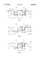
- FIG. 1is a diagram of an ESD protection cell according to the present invention prior to etch back of the antifuse material layer.
- FIG. 2is a diagram of an ESD protection cell according to the present invention after etch back of the antifuse material layer.
- FIG. 3is a diagram of an ESD protection cell according to the present invention in its completed state.
- FIG. 1shows an ESD protection cell 10 for use in protecting one or more antifuses 12.
- the essence hereis to fabricate the ESD protection cell 10 much like an antifuse cell 12 but with a degraded antifuse material layer which has been partially etched into in order to make it have a lower breakdown voltage and more leakage current.
- a substrate 18 containing diffusion regions 14, 16forms the base for the construction of antifuses and ESD protection cells.
- an interlayer dielectric layer 20formed preferably of a thermal oxide, which is etched back to form ESD protection cell openings 22 and antifuse cell openings 24 which expose the N+ diffusion regions 14, 16 within substrate 18 which will act as lower ESD protection cell and lower antifuse electrodes, respectively.
- antifuse material layer 26is then deposited over interlayer dielectric layer 20 and into cell openings 22, 24 so that is forms an electrical contact to the lower electrodes 14, 16.
- O--N--Ooxide-nitride-oxide
- Other types of antifuse materialcould also be used as would be known to those of ordinary skill in the art.
- Over the antifuse 12is then deposited a thin layer of doped or undoped polysilicon 34 which acts as a cap layer to protect antifuse material layer 26 in the region of antifuse 12.
- the antifuse material layer 26is then etched back to remove unprotected portions of oxide layer 32 and nitride layer 30 leaving oxide layer 28 to serve as the antifuse material layer for ESD protection cell 10.
- This operationcould be conducted to leave some or all of nitride layer 30 intact, similarly, etching into oxide layer 28 would do no harm as the goal is to have a poor performing antifuse structure for ESD protection cell 10.
- antifuse cell 12now consists of an intact antifuse material layer 26 together with a thin polysilicon layer 34 on top of it.
- a final polysilicon layer 36is deposited over both the ESD protection cells 10 and antifuses 12.
- the polysilicon layer 36is doped to serve as an electrode as is known by those of ordinary skill in the art and combines with polysilicon layer 34 so that polysilicon layers 34 and 36 serve together as the top electrode of antifuses 12.
- Polysilicon layer 36serves as the top ESD protection cell electrode and has an antifuse material layer 28 which is much weaker than antifuse material layer 26 so that it will easily break down in the presence of ESD to form a conductive link through layer 28 in the region of ESD protection cell 10 to bypass electrical charge which could damage antifuses 12.
- Interlayer dielectric layer 20has a thickness in the range of 500 ⁇ -4000 ⁇ with 1000 ⁇ presently preferred; oxide layer 28 has a thickness in the range of 10 ⁇ -60 ⁇ with 35 ⁇ presently preferred; nitride layer 30 has a thickness in the range of 40 ⁇ -200 ⁇ with 75 ⁇ presently preferred; oxide layer 32 has a thickness in the range of 10 ⁇ -60 ⁇ with 30 ⁇ presently preferred; polysilicon layer 34 has a thickness in the range of 50 ⁇ -3000 ⁇ with 200 ⁇ presently preferred and is presently preferred to be undoped; polysilicon layer 36 has a thickness in the range of 1000 ⁇ -4000 ⁇ with 2500 ⁇ presently preferred and is doped to a very low resistivity of about 4 ⁇ 10 -4 ohm-cm.
- the antifuse material layer in the region of the ESD protection cellwill have the same thickness as that of oxide layer 28. Because only high temperature materials are used in the antifuse and ESD protection cell, the processing of all of the steps described herein may be carried out in the range of 500° C.-1100° C. with 950° C. presently preferred. This high temperature processing yields better films and more reliable devices. High temperature processing also aids in the combination of polysilicon layer 34 and polysilicon layer 36 (since layers 34 and 36 are formed of the same material, they can thus be sintered and merged to form and behave as a single layer). An antifuse and ESD protection cell built in accordance with the foregoing description can be expected to have an antifuse programming voltage of about 10-30 volts and an ESD breakdown voltage of about 5 volts.
- lower electrodeshave been shown as diffusion-type electrodes, polysilicon electrodes could also be used for the lower electrodes as is well known to those of ordinary skill in the art.
Landscapes
- Engineering & Computer Science (AREA)
- Power Engineering (AREA)
- Physics & Mathematics (AREA)
- Condensed Matter Physics & Semiconductors (AREA)
- General Physics & Mathematics (AREA)
- Computer Hardware Design (AREA)
- Microelectronics & Electronic Packaging (AREA)
- Design And Manufacture Of Integrated Circuits (AREA)
- Semiconductor Memories (AREA)
Abstract
Description
Claims (4)
Priority Applications (1)
| Application Number | Priority Date | Filing Date | Title |
|---|---|---|---|
| US08/607,375US5656534A (en) | 1993-07-07 | 1996-02-27 | Method for forming an ESD protection device for antifuses with top polysilicon electrode |
Applications Claiming Priority (5)
| Application Number | Priority Date | Filing Date | Title |
|---|---|---|---|
| US08/087,942US5369054A (en) | 1993-07-07 | 1993-07-07 | Circuits for ESD protection of metal-to-metal antifuses during processing |
| US08/277,673US5519248A (en) | 1993-07-07 | 1994-07-19 | Circuits for ESD protection of metal-to-metal antifuses during processing |
| US08/289,678US5572061A (en) | 1993-07-07 | 1994-08-12 | ESD protection device for antifuses with top polysilicon electrode |
| US08/290,029US5498895A (en) | 1993-07-07 | 1994-08-12 | Process ESD protection devices for use with antifuses |
| US08/607,375US5656534A (en) | 1993-07-07 | 1996-02-27 | Method for forming an ESD protection device for antifuses with top polysilicon electrode |
Related Parent Applications (1)
| Application Number | Title | Priority Date | Filing Date |
|---|---|---|---|
| US08/289,678DivisionUS5572061A (en) | 1993-07-07 | 1994-08-12 | ESD protection device for antifuses with top polysilicon electrode |
Publications (1)
| Publication Number | Publication Date |
|---|---|
| US5656534Atrue US5656534A (en) | 1997-08-12 |
Family
ID=46249209
Family Applications (2)
| Application Number | Title | Priority Date | Filing Date |
|---|---|---|---|
| US08/289,678Expired - LifetimeUS5572061A (en) | 1993-07-07 | 1994-08-12 | ESD protection device for antifuses with top polysilicon electrode |
| US08/607,375Expired - Fee RelatedUS5656534A (en) | 1993-07-07 | 1996-02-27 | Method for forming an ESD protection device for antifuses with top polysilicon electrode |
Family Applications Before (1)
| Application Number | Title | Priority Date | Filing Date |
|---|---|---|---|
| US08/289,678Expired - LifetimeUS5572061A (en) | 1993-07-07 | 1994-08-12 | ESD protection device for antifuses with top polysilicon electrode |
Country Status (1)
| Country | Link |
|---|---|
| US (2) | US5572061A (en) |
Cited By (10)
| Publication number | Priority date | Publication date | Assignee | Title |
|---|---|---|---|---|
| US5913137A (en)* | 1993-07-07 | 1999-06-15 | Actel Corporation | Process ESD protection devices for use with antifuses |
| US6124193A (en)* | 1995-06-02 | 2000-09-26 | Actel Corporation | Raised tungsten plug antifuse and fabrication processes |
| US20010054740A1 (en)* | 1999-05-12 | 2001-12-27 | Micron Technology, Inc. | Adjustable high-trigger-voltage electrostatic discharge protection device |
| US6335228B1 (en)* | 1999-12-30 | 2002-01-01 | Infineon Technologies North America Corp. | Method for making an anti-fuse |
| US6627970B2 (en)* | 2000-12-20 | 2003-09-30 | Infineon Technologies Ag | Integrated semiconductor circuit, in particular a semiconductor memory circuit, having at least one integrated electrical antifuse structure, and a method of producing the structure |
| US20040036091A1 (en)* | 2002-07-08 | 2004-02-26 | Fifield John A. | High impedance antifuse |
| US20060249809A1 (en)* | 2005-05-06 | 2006-11-09 | Macronix International Co., Ltd. | Buried bit line anti-fuse one-time-programmable nonvolatile memory |
| US20070216015A1 (en)* | 2004-01-30 | 2007-09-20 | Koninklijke Philips Electronics N.V. | Integrated Circuit Chip With Electrostatic Discharge Protection Device |
| CN100452392C (en)* | 2003-05-22 | 2009-01-14 | 统宝光电股份有限公司 | Electrostatic discharge protection element with thick film polysilicon, electronic device and manufacturing method |
| DE102019000164A1 (en)* | 2019-01-11 | 2020-07-16 | Tdk-Micronas Gmbh | Lateral, once programmable memory component |
Families Citing this family (10)
| Publication number | Priority date | Publication date | Assignee | Title |
|---|---|---|---|---|
| US5844297A (en)* | 1995-09-26 | 1998-12-01 | Symbios, Inc. | Antifuse device for use on a field programmable interconnect chip |
| US6114862A (en)* | 1996-02-14 | 2000-09-05 | Stmicroelectronics, Inc. | Capacitive distance sensor |
| US5661071A (en)* | 1996-04-01 | 1997-08-26 | Chartered Semiconductor Manufacturing Pte Ltd | Method of making an antifuse cell with tungsten silicide electrode |
| US6091082A (en)* | 1998-02-17 | 2000-07-18 | Stmicroelectronics, Inc. | Electrostatic discharge protection for integrated circuit sensor passivation |
| US6433403B1 (en)* | 1999-04-21 | 2002-08-13 | Micron Technology, Inc. | Integrated circuit having temporary conductive path structure and method for forming the same |
| KR100306469B1 (en) | 1999-08-27 | 2001-11-01 | 윤종용 | Circuit and Method for Fuse Option in Integrate Circuit |
| US6388305B1 (en)* | 1999-12-17 | 2002-05-14 | International Business Machines Corporation | Electrically programmable antifuses and methods for forming the same |
| TW584953B (en)* | 2003-04-25 | 2004-04-21 | Toppoly Optoelectronics Corp | ESD protection device with thick poly film, electronic device and method for forming the same |
| JP5387677B2 (en)* | 2009-07-09 | 2014-01-15 | 株式会社村田製作所 | Antifuse element |
| CN106653842B (en)* | 2015-10-28 | 2019-05-17 | 无锡华润上华科技有限公司 | A kind of semiconductor devices with electrostatic discharge protection structure |
Citations (15)
| Publication number | Priority date | Publication date | Assignee | Title |
|---|---|---|---|---|
| US4748490A (en)* | 1985-08-01 | 1988-05-31 | Texas Instruments Incorporated | Deep polysilicon emitter antifuse memory cell |
| US4821096A (en)* | 1985-12-23 | 1989-04-11 | Intel Corporation | Excess energy protection device |
| US4823181A (en)* | 1986-05-09 | 1989-04-18 | Actel Corporation | Programmable low impedance anti-fuse element |
| US4829350A (en)* | 1988-05-05 | 1989-05-09 | National Semiconductor Corporation | Electrostatic discharge integrated circuit protection |
| US4862243A (en)* | 1987-06-01 | 1989-08-29 | Texas Instruments Incorporated | Scalable fuse link element |
| US4899205A (en)* | 1986-05-09 | 1990-02-06 | Actel Corporation | Electrically-programmable low-impedance anti-fuse element |
| US4941028A (en)* | 1988-08-10 | 1990-07-10 | Actel Corporation | Structure for protecting thin dielectrics during processing |
| US5070384A (en)* | 1990-04-12 | 1991-12-03 | Actel Corporation | Electrically programmable antifuse element incorporating a dielectric and amorphous silicon interlayer |
| US5111262A (en)* | 1988-08-10 | 1992-05-05 | Actel Corporation | Structure for protecting thin dielectrics during processing |
| US5166556A (en)* | 1991-01-22 | 1992-11-24 | Myson Technology, Inc. | Programmable antifuse structure, process, logic cell and architecture for programmable integrated circuits |
| US5171715A (en)* | 1991-11-12 | 1992-12-15 | Actel Corporation | Process for fabricating electrically programmable antifuse element |
| US5233217A (en)* | 1991-05-03 | 1993-08-03 | Crosspoint Solutions | Plug contact with antifuse |
| US5290734A (en)* | 1991-06-04 | 1994-03-01 | Vlsi Technology, Inc. | Method for making anti-fuse structures |
| US5341267A (en)* | 1991-09-23 | 1994-08-23 | Aptix Corporation | Structures for electrostatic discharge protection of electrical and other components |
| US5498895A (en)* | 1993-07-07 | 1996-03-12 | Actel Corporation | Process ESD protection devices for use with antifuses |
Family Cites Families (2)
| Publication number | Priority date | Publication date | Assignee | Title |
|---|---|---|---|---|
| US5989943A (en)* | 1989-09-07 | 1999-11-23 | Quicklogic Corporation | Method for fabrication of programmable interconnect structure |
| GB2278964B (en)* | 1993-06-04 | 1996-12-04 | Wei Hong Shen | Track-mounted lighting fixture |
- 1994
- 1994-08-12USUS08/289,678patent/US5572061A/ennot_activeExpired - Lifetime
- 1996
- 1996-02-27USUS08/607,375patent/US5656534A/ennot_activeExpired - Fee Related
Patent Citations (15)
| Publication number | Priority date | Publication date | Assignee | Title |
|---|---|---|---|---|
| US4748490A (en)* | 1985-08-01 | 1988-05-31 | Texas Instruments Incorporated | Deep polysilicon emitter antifuse memory cell |
| US4821096A (en)* | 1985-12-23 | 1989-04-11 | Intel Corporation | Excess energy protection device |
| US4823181A (en)* | 1986-05-09 | 1989-04-18 | Actel Corporation | Programmable low impedance anti-fuse element |
| US4899205A (en)* | 1986-05-09 | 1990-02-06 | Actel Corporation | Electrically-programmable low-impedance anti-fuse element |
| US4862243A (en)* | 1987-06-01 | 1989-08-29 | Texas Instruments Incorporated | Scalable fuse link element |
| US4829350A (en)* | 1988-05-05 | 1989-05-09 | National Semiconductor Corporation | Electrostatic discharge integrated circuit protection |
| US4941028A (en)* | 1988-08-10 | 1990-07-10 | Actel Corporation | Structure for protecting thin dielectrics during processing |
| US5111262A (en)* | 1988-08-10 | 1992-05-05 | Actel Corporation | Structure for protecting thin dielectrics during processing |
| US5070384A (en)* | 1990-04-12 | 1991-12-03 | Actel Corporation | Electrically programmable antifuse element incorporating a dielectric and amorphous silicon interlayer |
| US5166556A (en)* | 1991-01-22 | 1992-11-24 | Myson Technology, Inc. | Programmable antifuse structure, process, logic cell and architecture for programmable integrated circuits |
| US5233217A (en)* | 1991-05-03 | 1993-08-03 | Crosspoint Solutions | Plug contact with antifuse |
| US5290734A (en)* | 1991-06-04 | 1994-03-01 | Vlsi Technology, Inc. | Method for making anti-fuse structures |
| US5341267A (en)* | 1991-09-23 | 1994-08-23 | Aptix Corporation | Structures for electrostatic discharge protection of electrical and other components |
| US5171715A (en)* | 1991-11-12 | 1992-12-15 | Actel Corporation | Process for fabricating electrically programmable antifuse element |
| US5498895A (en)* | 1993-07-07 | 1996-03-12 | Actel Corporation | Process ESD protection devices for use with antifuses |
Cited By (21)
| Publication number | Priority date | Publication date | Assignee | Title |
|---|---|---|---|---|
| US5913137A (en)* | 1993-07-07 | 1999-06-15 | Actel Corporation | Process ESD protection devices for use with antifuses |
| US6124193A (en)* | 1995-06-02 | 2000-09-26 | Actel Corporation | Raised tungsten plug antifuse and fabrication processes |
| US20010054740A1 (en)* | 1999-05-12 | 2001-12-27 | Micron Technology, Inc. | Adjustable high-trigger-voltage electrostatic discharge protection device |
| US6335228B1 (en)* | 1999-12-30 | 2002-01-01 | Infineon Technologies North America Corp. | Method for making an anti-fuse |
| US6627970B2 (en)* | 2000-12-20 | 2003-09-30 | Infineon Technologies Ag | Integrated semiconductor circuit, in particular a semiconductor memory circuit, having at least one integrated electrical antifuse structure, and a method of producing the structure |
| US20040036091A1 (en)* | 2002-07-08 | 2004-02-26 | Fifield John A. | High impedance antifuse |
| US6753590B2 (en)* | 2002-07-08 | 2004-06-22 | International Business Machines Corporation | High impedance antifuse |
| US7098083B2 (en)* | 2002-07-08 | 2006-08-29 | International Business Machines Corporation | High impedance antifuse |
| US7981731B2 (en) | 2002-07-08 | 2011-07-19 | International Business Machines Corporation | Method of forming a high impedance antifuse |
| US20060289864A1 (en)* | 2002-07-08 | 2006-12-28 | Fifield John A | High impedance antifuse |
| CN100452392C (en)* | 2003-05-22 | 2009-01-14 | 统宝光电股份有限公司 | Electrostatic discharge protection element with thick film polysilicon, electronic device and manufacturing method |
| US20070216015A1 (en)* | 2004-01-30 | 2007-09-20 | Koninklijke Philips Electronics N.V. | Integrated Circuit Chip With Electrostatic Discharge Protection Device |
| US7638855B2 (en)* | 2005-05-06 | 2009-12-29 | Macronix International Co., Ltd. | Anti-fuse one-time-programmable nonvolatile memory |
| US20090323388A1 (en)* | 2005-05-06 | 2009-12-31 | Macronix International Co., Ltd. | Buried Bit Line Anti-Fuse One-Time-Programmable Nonvolatile Memory |
| US7786000B2 (en)* | 2005-05-06 | 2010-08-31 | Macronix International Co., Ltd. | Buried bit line anti-fuse one-time-programmable nonvolatile memory |
| US20100296328A1 (en)* | 2005-05-06 | 2010-11-25 | Macronix International Co., Ltd. | Buried bit line anti-fuse one-time-programmable nonvolatile memory |
| US20060249809A1 (en)* | 2005-05-06 | 2006-11-09 | Macronix International Co., Ltd. | Buried bit line anti-fuse one-time-programmable nonvolatile memory |
| US8476157B2 (en) | 2005-05-06 | 2013-07-02 | Macronix International Co., Ltd. | Buried bit line anti-fuse one-time-programmable nonvolatile memory |
| US8679917B2 (en) | 2005-05-06 | 2014-03-25 | Macronix International Co., Ltd. | Buried bit line anti-fuse one-time-programmable nonvolatile memory |
| DE102019000164A1 (en)* | 2019-01-11 | 2020-07-16 | Tdk-Micronas Gmbh | Lateral, once programmable memory component |
| DE102019000164B4 (en)* | 2019-01-11 | 2020-09-10 | Tdk-Micronas Gmbh | Lateral one-time programmable memory device |
Also Published As
| Publication number | Publication date |
|---|---|
| US5572061A (en) | 1996-11-05 |
Similar Documents
| Publication | Publication Date | Title |
|---|---|---|
| US5656534A (en) | Method for forming an ESD protection device for antifuses with top polysilicon electrode | |
| US5903041A (en) | Integrated two-terminal fuse-antifuse and fuse and integrated two-terminal fuse-antifuse structures incorporating an air gap | |
| US5670403A (en) | Dielectric-polysilicon-dielectric antifuse for field programmable logic applications | |
| US5629227A (en) | Process of making ESD protection devices for use with antifuses | |
| KR100230158B1 (en) | Anti-fuse structure and manufacturing method with reduced leakage current | |
| US5920109A (en) | Raised tungsten plug antifuse and fabrication processes | |
| KR100299340B1 (en) | Antifuse structure and process | |
| US6222221B1 (en) | Cross-coupled capacitors for improved voltage coefficient | |
| US5789764A (en) | Antifuse with improved antifuse material | |
| JP3407204B2 (en) | Ferroelectric integrated circuit and method of manufacturing the same | |
| US5369054A (en) | Circuits for ESD protection of metal-to-metal antifuses during processing | |
| KR100866960B1 (en) | Semiconductor integrated circuit | |
| US6933551B1 (en) | Large value, compact, high yielding integrated circuit capacitors | |
| WO2006107384A1 (en) | Antifuse element and electrically redundant antifuse array for controlled rupture location | |
| JP2002507062A (en) | Overvoltage protection device for integrated circuits | |
| US5786613A (en) | Integrated overvoltage protection device having electrodes separated by a gas-filled cavity | |
| US6882027B2 (en) | Methods and apparatus for providing an antifuse function | |
| US7390726B1 (en) | Switching ratio and on-state resistance of an antifuse programmed below 5 mA and having a Ta or TaN barrier metal layer | |
| US6291871B1 (en) | Method of jointly forming stacked capacitors and antifuses, method of blowing antifuses, and antifuses and stacked capacitors constituting a part of integrated circuitry | |
| US6384452B1 (en) | Electrostatic discharge protection device with monolithically formed resistor-capacitor portion | |
| US6060347A (en) | Method for preventing damage to gate oxide from well in complementary metal-oxide semiconductor | |
| US6414369B1 (en) | Thin film capacitor element | |
| US5434448A (en) | Programmable contact structure | |
| JPH04229636A (en) | Electronic element | |
| US5449938A (en) | MOS-controlled power semiconductor component |
Legal Events
| Date | Code | Title | Description |
|---|---|---|---|
| FEPP | Fee payment procedure | Free format text:PAYOR NUMBER ASSIGNED (ORIGINAL EVENT CODE: ASPN); ENTITY STATUS OF PATENT OWNER: LARGE ENTITY | |
| FPAY | Fee payment | Year of fee payment:4 | |
| FPAY | Fee payment | Year of fee payment:8 | |
| REMI | Maintenance fee reminder mailed | ||
| LAPS | Lapse for failure to pay maintenance fees | ||
| STCH | Information on status: patent discontinuation | Free format text:PATENT EXPIRED DUE TO NONPAYMENT OF MAINTENANCE FEES UNDER 37 CFR 1.362 | |
| FP | Lapsed due to failure to pay maintenance fee | Effective date:20090812 | |
| AS | Assignment | Owner name:MORGAN STANLEY & CO. INCORPORATED, NEW YORK Free format text:PATENT SECURITY AGREEMENT;ASSIGNORS:WHITE ELECTRONIC DESIGNS CORP.;ACTEL CORPORATION;MICROSEMI CORPORATION;REEL/FRAME:025783/0613 Effective date:20110111 | |
| AS | Assignment | Owner name:MICROSEMI SEMICONDUCTOR (U.S.) INC., A DELAWARE CO Free format text:RELEASE BY SECURED PARTY;ASSIGNOR:BANK OF AMERICA, N.A.;REEL/FRAME:037558/0711 Effective date:20160115 Owner name:MICROSEMI CORP.-ANALOG MIXED SIGNAL GROUP, A DELAW Free format text:RELEASE BY SECURED PARTY;ASSIGNOR:BANK OF AMERICA, N.A.;REEL/FRAME:037558/0711 Effective date:20160115 Owner name:MICROSEMI FREQUENCY AND TIME CORPORATION, A DELAWA Free format text:RELEASE BY SECURED PARTY;ASSIGNOR:BANK OF AMERICA, N.A.;REEL/FRAME:037558/0711 Effective date:20160115 Owner name:MICROSEMI SOC CORP., A CALIFORNIA CORPORATION, CAL Free format text:RELEASE BY SECURED PARTY;ASSIGNOR:BANK OF AMERICA, N.A.;REEL/FRAME:037558/0711 Effective date:20160115 Owner name:MICROSEMI COMMUNICATIONS, INC. (F/K/A VITESSE SEMI Free format text:RELEASE BY SECURED PARTY;ASSIGNOR:BANK OF AMERICA, N.A.;REEL/FRAME:037558/0711 Effective date:20160115 Owner name:MICROSEMI CORPORATION, CALIFORNIA Free format text:RELEASE BY SECURED PARTY;ASSIGNOR:BANK OF AMERICA, N.A.;REEL/FRAME:037558/0711 Effective date:20160115 Owner name:MICROSEMI CORP.-MEMORY AND STORAGE SOLUTIONS (F/K/ Free format text:RELEASE BY SECURED PARTY;ASSIGNOR:BANK OF AMERICA, N.A.;REEL/FRAME:037558/0711 Effective date:20160115 |