US5654984A - Signal modulation across capacitors - Google Patents
Signal modulation across capacitorsDownload PDFInfo
- Publication number
- US5654984A US5654984AUS08/161,741US16174193AUS5654984AUS 5654984 AUS5654984 AUS 5654984AUS 16174193 AUS16174193 AUS 16174193AUS 5654984 AUS5654984 AUS 5654984A
- Authority
- US
- United States
- Prior art keywords
- signal
- coupled
- node
- circuit
- modulator
- Prior art date
- Legal status (The legal status is an assumption and is not a legal conclusion. Google has not performed a legal analysis and makes no representation as to the accuracy of the status listed.)
- Expired - Lifetime
Links
Images


Classifications
- H—ELECTRICITY
- H04—ELECTRIC COMMUNICATION TECHNIQUE
- H04B—TRANSMISSION
- H04B5/00—Near-field transmission systems, e.g. inductive or capacitive transmission systems
- H04B5/70—Near-field transmission systems, e.g. inductive or capacitive transmission systems specially adapted for specific purposes
- H04B5/75—Near-field transmission systems, e.g. inductive or capacitive transmission systems specially adapted for specific purposes for isolation purposes
- H—ELECTRICITY
- H04—ELECTRIC COMMUNICATION TECHNIQUE
- H04B—TRANSMISSION
- H04B5/00—Near-field transmission systems, e.g. inductive or capacitive transmission systems
- H04B5/20—Near-field transmission systems, e.g. inductive or capacitive transmission systems characterised by the transmission technique; characterised by the transmission medium
- H04B5/22—Capacitive coupling
- H—ELECTRICITY
- H04—ELECTRIC COMMUNICATION TECHNIQUE
- H04L—TRANSMISSION OF DIGITAL INFORMATION, e.g. TELEGRAPHIC COMMUNICATION
- H04L25/00—Baseband systems
- H04L25/02—Details ; arrangements for supplying electrical power along data transmission lines
- H04L25/0264—Arrangements for coupling to transmission lines
- H04L25/0266—Arrangements for providing Galvanic isolation, e.g. by means of magnetic or capacitive coupling
- H04L25/0268—Arrangements for providing Galvanic isolation, e.g. by means of magnetic or capacitive coupling with modulation and subsequent demodulation
- H—ELECTRICITY
- H04—ELECTRIC COMMUNICATION TECHNIQUE
- H04L—TRANSMISSION OF DIGITAL INFORMATION, e.g. TELEGRAPHIC COMMUNICATION
- H04L7/00—Arrangements for synchronising receiver with transmitter
- H04L7/0008—Synchronisation information channels, e.g. clock distribution lines
- H—ELECTRICITY
- H04—ELECTRIC COMMUNICATION TECHNIQUE
- H04M—TELEPHONIC COMMUNICATION
- H04M11/00—Telephonic communication systems specially adapted for combination with other electrical systems
- H04M11/06—Simultaneous speech and data transmission, e.g. telegraphic transmission over the same conductors
- H—ELECTRICITY
- H01—ELECTRIC ELEMENTS
- H01F—MAGNETS; INDUCTANCES; TRANSFORMERS; SELECTION OF MATERIALS FOR THEIR MAGNETIC PROPERTIES
- H01F38/00—Adaptations of transformers or inductances for specific applications or functions
- H01F38/14—Inductive couplings
- H01F2038/146—Inductive couplings in combination with capacitive coupling
Definitions
- the present inventionrelates to the coupling of signals across capacitors.
- Circuitry for coupling a signalunder such circumstances must provide for the isolation of the voltages of the different circuits to prevent interference or damage to the circuits from voltages exceeding the intended operational voltage ranges of the circuits.
- Circuitry for coupling a signalunder such circumstances must provide for the isolation of the voltages of the different circuits to prevent interference or damage to the circuits from voltages exceeding the intended operational voltage ranges of the circuits.
- a computerwhen interfering a computer to a telephone line, such as with a modem, it is necessary to provide isolation between the circuits of the computer, which operate at controlled low voltages, and the telephone line, where voltages over a very wide range, including high voltages, may be present. While such isolation is necessary, it must be accomplished in a manner that allows the coupling of signals between the computer and the telephone line without undesirable levels of distortion, attenuation, or other degradation of the signals.
- isolation transformermagnetically couples signals between its windings while keeping the windings electrically isolated from one another. Since DC components of a signal do not pass through the isolation transformer, DC potentials on opposite sides of the isolation transformer are isolated from one another.
- An isolation transformercomprises a core of magnetic material and a plurality of windings. Since the minimum size of the core and windings is dictated by the desired electrical parameters of the transformer, the size of the transformer cannot be reduced below that minimum. Thus, isolation transformers are typically relatively large and bulky. They often have dimensions that are inconsistent with miniaturized packaging configurations. Isolation transformers are also usually rather expensive since the require production and assembly of specialized magnetic materials, insulated wire, insulating materials, and connection terminals.
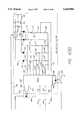
- FIG. 1is a diagram of a telephone line interface circuit of the prior art.
- Telephone line 105which comprises tip and ring conductors, is coupled to protection devices and DC holding circuit 101.
- Protection devices and DC holding circuit 101is coupled to node 108, which is coupled to a first terminal of a first winding of transformer 103.
- Protection devices and DC holding circuit 101is also coupled to node 109, which is coupled to a second terminal of the first winding of transformer 103.
- a first terminal of the second winding of transformer 103is coupled to node 110, which is coupled to transmit and receive circuits 102.
- a second terminal of the second winding of transformer 103is coupled to node 111, which is coupled to transmit and receive circuits 102.
- Transmit signal TXis applied to node 106, which is coupled to transmit and receive circuits 102.
- Transmit signal TXis applied to node 106, which is coupled to transmit and receive circuits 102.
- Transmit and receive circuits 102are coupled to node 107, which provides receive signal RX.
- the first winding and the second winding of transformer 103are isolated from each other so as to maintain high voltage barrier 104. Thus, great voltage differences between the circuits on the two sides of high voltage barrier 104 may exist without harm or interference to circuits on the other side of high voltage barrier 104.
- Any signals desired to be transmitted over telephone line 105are applied as signal TX at node 106.
- the signal to be transmittedis processed by transmit and receive circuits 102 and applied across nodes 110 and 111.
- the signalsare coupled across coupling transformer 103 to nodes 108 and 109.
- the signalspass through protection devices and DC holding circuit 101 to be applied to telephone line 105.
- Signals on telephone line 105pass through protection devices and DC holding circuit 101, through nodes 108 and 109 to transformer 103.
- Transformer 103couples the receive signals to nodes 110 and 111, which couple the receive signals to transmit and receive circuits 102.
- Transmit and receive circuits 102output the receive signals at 107, which provides receive signal RX.
- Optocouplersinclude an LED having its light output coupled to a phototransistor, photodiode, or other photosensitive device, with the assembly encapsulated in an opaque package. Since optocouplers rely on LEDs, which do not exhibit linear response, optocouplers are generally used to transmit signals of a digital nature, which do not require linear devices for transmission. Moreover, reasonably priced optocouplers are generally too slow to provide sufficient transmission quality.
- Capacitorsare used to couple signals. Since the frequency range of the signals that may be coupled is related to the value of the capacitors, only signals of certain frequency ranges may be coupled by capacitors of particular values. Capacitors typically have a size proportional to their value. Also, there is typically an inverse relationship between the value of a capacitor and the frequencies that it will pass. Thus, a large capacitor is usually required to pass low frequency signals, for example, audio frequencies. Large capacitors are often too large and bulky to be accommodated by miniaturized packaging configurations. Large capacitors are also more expensive.
- the present inventionprovides a method and apparatus for communicating a signal across a capacitive isolation barrier using sigma delta modulation.
- the present inventionallows low distortion communication of an audio signal across an isolation barrier without the need for a large and bulky isolation transformer, a large and bulky capacitor, or an optocoupler.
- the present inventionuses a sigma delta modulator to convert an analog signal to a binary signal having a pulse density dependent on the amplitude of the analog signal.
- the pulse duration of the binary signalis preferably on the order of microseconds or fractions of microseconds, resulting in a binary signal that includes frequencies on the order of megahertz (MHz). Signals in the megahertz range can be effectively coupled by small capacitors, unlike signals in the audio frequency range. Thus, the need for large, bulky capacitors is avoided.
- the analog signal provided to the sigma delta modulatoris first filtered to limit the bandwidth of the signal and to prevent aliasing.
- the filtered analog signalis then applied to the sigma delta modulator, which provides a binary signal.
- the binary signal provided by the sigma delta modulatoris communicated across a capacitor, which may have a value in the picofarad range, and received by a digital-to-analog (D/A) converter or by digital signal processing (DSP) circuitry. If the signal is received by a D/A converter, the D/A converter converts the binary signal to an analog signal.
- the analog signalis then filtered to remove noise that might otherwise result from the digital conversion and processing of the signal. If the signal is received by DSP circuitry, the DSP circuitry processes the signal digitally.
- the present inventionmay be used to provide telephone line isolation for modem applications compliant with governmental regulations.
- a line interface integrated circuitmay be connected directly to a telephone line and powered by the telephone line.
- the line interface ICmay include a sigma delta modulator to communicate the receive signal across a capacitive isolation barrier and a digital-to-analog (D/A) converter to provide an analog transmit signal from a sigma delta bit stream communicated across a capacitive isolation barrier.
- Circuitry on the opposite side of the capacitive isolation barrierincludes similar components to process the transmit and receive signals.
- the present inventionmay be practiced at high frequencies (e.g. on the order of megahertz), allowing use of small capacitors (e.g. on the order of picofarads) to provide the high voltage isolation barrier. Circuitry on the telephone line side of the high voltage isolation barrier may derive its power from the telephone line, minimizing power supply requirements. Furthermore, since modern line interface circuits require A/D and D/A conversion, very little additional circuitry is needed to communicate signals across an isolation barrier according to the present invention. Thus, the disadvantages of the prior art have been overcome.
- FIG. 1is a diagram of a telephone line interface circuit of the prior art.
- FIG. 2is a block diagram of the preferred embodiment of the present invention.
- FIG. 3is a block diagram illustrating a system comprising an embodiment of the present invention.
- FIG. 4is a block diagram of a system comprising an embodiment of the present invention.
- FIGS. 5A and 5Billustrate an example of sigma delta modulation.
- FIG. 5Aillustrates an analog signal Waveform 501 illustrates one cycle of an sine wave.
- FIG. 5Billustrates a sigma delta bit stream derived from the analog signal of FIG. 5A.
- FIGS. 6(A) and 6(B)illustrate a diagram of a system that comprises an embodiment of the present invention.
- FIG. 7is a diagram illustrating the respective orientation of FIGS. 7(A), 7(B), 7(C), and 7(D) relative to one another.
- FIGS. 7(A), 7(B), 7(C), and 7(D)illustrate schematic diagram illustrating a circuit comprising an embodiment of the present invention.
- FIGS. 8A and 8Billustrate an example of Manchester encoded sigma delta modulation.
- FIG. 9is a block diagram of a system comprising an embodiment of the present invention.
- FIG. 10is a block diagram illustrating a digital signal processing (DSP) sub-system for use with the present invention.
- DSPdigital signal processing
- the present inventionuses a sigma delta modulation technique to couple an analog signal across a capacitive isolation barrier. Since sigma delta modulation is often used to provide conversion between analog and digital forms of a signal (either A/D or D/A conversion), the need for extra circuitry beyond that which would otherwise be needed for conversion is minimized.
- the present inventionuses sigma delta modulation both to facilitate analog-to-digital conversion and to provide a modulated signal suitable for transmission across a capacitive isolation barrier. By providing sigma delta modulation of signals on both sides of the isolation barrier, bidirectional communication across the isolation barrier may be provided.
- the present inventionis useful in telephone line interface applications, especially applications where a computer is interfaced to a telephone line, for example, with a modem.
- One side of the isolation barriermay be coupled to the telephone line, while the other side of the isolation barrier may be coupled to a computer or other user device, such as a telephone instrument.
- the present inventionprovides bidirectional coupling of audio signals across the isolation barrier in a manner that complies with regulatory requirements. Coupling of digital signals, such as digital control signals, is optionally provided via optocouplers.
- Portions of the conversion circuitrymay be located on each side of the isolation barrier, with the sigma delta modulated signal coupled across the isolation barrier. Portions of the circuitry on the telephone line side may derive their power from the telephone line, while portions on the computer or subscriber side may derive their power from the computer power supply or another power source on the subscriber side, thereby minimizing power supply complexity and reducing the amount of power supplied by the computer power supply.
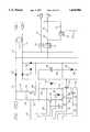
- FIG. 2is a block diagram of the preferred embodiment of the present invention.
- Telephone line 209which comprises tip and ring conductors, is coupled to block 201.
- Block 201is coupled through node 212 to a first terminal of capacitor 203, through node 214 to a first terminal of capacitor 204, and through node 216 to a first terminal of capacitor 205.
- Block 201is also coupled through node 218 to the anode of the LED of optocoupler 206 and through node 220 to the collector of the photo transistor of optocoupler 207.
- the cathode of the LED of optocoupler 206is coupled to ground.
- the emitter of the photo transistor of optocoupler 207is coupled to ground.
- Block 202is coupled through node 213 to the second terminal of capacitor 203, through node 215 to the second terminal of capacitor 204, and through node 217 to the second terminal of capacitor 205.
- Block 202is also coupled through node 219 to the collector of the photo transistor of optocoupler 206 and through node 221 to the anode of the LED of optocoupler 207.
- the emitter of the photo transistor of optocoupler 206is coupled to ground.
- Block 202provides receive signal RX through node 210.
- Block 201comprises filter block 222, sigma delta modulator block 223, digital to analog (D/A) converter block 224, dock receiver block 225, optocoupler driver block 226, and optocoupler receiver block 227.
- Block 202comprises filter block 228, sigma delta modulator 229, D/A converter 230, clock oscillator 231, optocoupler receiver 232, and optocoupler driver 233.
- the tip and ring conductors of telephone line 209are coupled to filter block 222.
- a receive signal from filter block 222is coupled through node 234 to sigma delta modulator 223.
- Sigma delta modulator 223provides a pulse density or sigma delta modulated version of the receive signal at node 212.
- the pulses of the sigma delta modulated signal at node 212are coupled through capacitor 203 to node 213.
- D/A converter 230receives the sigma delta bit stream at node 213 and converts it to an analog signal at node 236.
- the signal from node 236passes through filter block 228 and is output as receive signal RX at node 210. Transmit signal TX at node 211 is applied to filter block 228.
- Filter block 228provides an output at node 237 to sigma delta modulator 229.
- Sigma delta modulator 229provides a bit density or sigma delta modulated bit stream based on the transmit signal TX at node 217.
- the sigma delta bit stream at node 217is coupled through capacitor 205 to node 216.
- the sigma delta bit stream signal at node 216is coupled to D/A converter 224.
- D/A converter 224converts the sigma delta bit stream signal at node 216 to an analog output at node 235.
- the signal at node 235is coupled to filter block 222.
- Filter block 222provides an output signal across the tip and ring conductors of telephone line 209.
- Optocoupler driver block 226provides a signal at node 218 to drive Optocoupler 206.
- Optocoupler 206couples the signal at node 218 across barrier 208 to node 219.
- the signal at node 219is received by optocoupler receiver block 232.
- Optocoupler driver block 233provides a signal at node 221 to drive optocoupler 207.
- Optocoupler 207couples the signal at node 221 across high voltage barrier 208 to node 220.
- the signal at node 220is received by optocoupler receiver block 227.
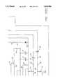
- FIG. 3is a block diagram illustrating a system comprising an embodiment of the present invention.
- the systemmay be used to implement a modem for communication of digital information over a telephone line.
- a tip and ring conductors of telephone line 309are coupled to analog front end line interface circuit 310.
- Analog front end line interface circuit 301is coupled through node 312 to a first terminal of capacitor 303, through node 314 to a first terminal of capacitor 304, and through node 316 to a first terminal of capacitor 305.
- Analog front end line interface circuit 301is also coupled through node 318 to optocoupler 306 and through node 320 to optocoupler 307.
- Capacitors 303, 304, and 305 and optocouplers 306 and 307maintain high voltage barrier 308.
- Signal processing circuit 302is coupled through node 313 to a second terminal of capacitor 303, through node 315 to a second terminal of capacitor 304, and through node 317 to a second terminal of capacitor 305.
- Processor 322is also coupled through node 319 to optocoupler 306 and through node 321 to optocoupler 307.
- Signal processing circuit 302is coupled through nodes 310 and 311 to processor 322.
- Signal processing circuit 302may be a digital signal processing (DSP) circuit or other signal processing circuitry, such as a D/A converter.
- Processor 322may be a central processing unit (CPU), microcontrol unit (MCU), such as a single IC microcontroller, or any other type of digital processor.
- FIG. 4is a block diagram of a system comprising an embodiment of the present invention.
- Node 406is coupled to anti-alias filter block 401.
- Anti-alias filter block 401is coupled through node 407 to sigma delta modulator block 402.
- Sigma delta modulator block 402is coupled through node 408 to a first terminal of capacitor of 405.
- a second terminal of capacitor 405is coupled through node 409 to one bit D/A converter block 403.
- One bit D/A converter block 403is coupled through node 410 to low pass filter 404.
- Low pass filter 404is coupled to node 411.
- a signal at node 406is filtered by anti-alias filter block 401 to prepare the signal for sigma delta modulation and to avoid aliasing.
- Anti-alias filter block 401may optionally include a high pass filter to block DC voltages and any other undesired low frequency signals.
- the filtered signalis passed from anti alias filter block 401 through node 407 to sigma delta modulator 402.
- Sigma delta modulator block 402produces a sigma delta bit stream at node 408 based on the signal at node 407.
- the signal at node 408is coupled to node 409 through capacitor 405.
- Capacitor 405provides a high voltage barrier between nodes 408 and 409 to prevent unwanted voltages, such as DC voltages, from passing between nodes 408 and 409.
- the sigma delta bit stream at node 409is converted to an analog signal at node 410 by one bit D/A converter 403.
- the analog signal at node 410is low pass filtered by low pass filter 404 to provide an output signal at node 411.
- FIG. 9is a block diagram of a system comprising an embodiment of the present invention.
- Node 911is coupled to anti-alias filter block. 901.
- Anti-alias filter block 901is coupled through node 912 to sigma delta modulator block 902.
- Sigma delta modulator block 902is coupled through node 913 to a first terminal of capacitor of 909.
- a second terminal of capacitor 909is coupled through node 914 to digital sigma delta demodulator block 903.
- Digital sigma delta demodulator block 903is coupled through node 915 to digital filter 904.
- Digital filter 904is coupled to node 916.
- a signal at node 911is filtered by anti-alias filter block 901 to prepare the signal for sigma delta modulation and to avoid aliasing.
- Anti-alias filter block 901may optionally include a high pass filter to block DC voltages and any other undesired low frequency signals.
- the filtered signalis passed from anti alias filter block 901 through node 912 to sigma delta modulator 902.
- Sigma delta modulator block 902produces a sigma delta bit stream at node 913 based on the signal at node 912.
- the signal at node 913is coupled to node 914 through capacitor 909.
- Capacitor 909provides a high voltage barrier between nodes 913 and 914 to prevent unwanted voltages, such as DC voltages, from passing between nodes 913 and 914.
- the sigma delta bit stream at node 914is demodulated by digital sigma delta demodulator 903 to provide a digital signal at node 915.
- the digital signal at node 915is digitally filtered by digital filter 904 to provide a digital output signal at node 916.
- the digital output signal at node 916may be additionally processed using DSP circuitry, may be applied to a computer, CPU, microcontroller or MCU, or may be converted to an analog form.
- a digital input signalis applied to node 917.
- Digital signal processing (DSP) circuit 905processes the signal digitally to provide a digital signal at node 918.
- Digital sigma delta modulator block 906converts the digital signal at node 918 to a sigma delta modulated signal at node 919 that is coupled through capacitor 910 to node 920.
- D/A converter 907converts the digital signal at node 907 to an analog signal at node 921.
- Low pass filter 908filters the analog signal at node 921 to remove any unwanted high frequency signals, such as those related to the sigma delta modulated process or the D/A conversion process, thus providing an analog output signal at node 922 having low distortion.
- Nodes 911 and 922may be coupled to a telephone line to allow reception and transmission of signals .over a telephone line.
- FIGS. 5A and 5Billustrate an example of sigma delta modulation.
- FIG. 5Aillustrates an analog signal.
- Waveform 501illustrates one cycle of a sine wave.
- FIG. 5Billustrates a sigma delta bit stream derived from the analog signal of FIG. 5A.
- the sigma delta bit streamis illustrated by waveform 502.
- Waveform 502is a digital signal that may have an instantaneous level of high level 528 or low level 529. Waveform 502 may transition between levels at regular clock intervals as illustrated by times 503 through 527. For example, waveform 502 is at low level 529 prior to time 503. At time 503, waveform 502 transitions to high level 528. At time 504, waveform 502 transitions from high level 528 back to low level 529.
- Waveform 502is dependent upon waveform 501.
- the number of pulses of waveform 502 having a low level 529increases over portions of waveform 502 corresponding to portions of waveform 501 that have a more negative value along axis 533.
- the likelihood that waveform 502 will be at high level 528is dependent upon the location of the corresponding point of waveform 510 along axis 533, with the likelihood increasing in the positive direction of axis 533 and decreasing in the negative direction of axis 533.
- FIGS. 8A and 8Billustrate an example of Manchester encoded sigma delta modulation.
- FIG. 8Aillustrates an analog signal.
- Waveform 801illustrates one cycle of a sine wave.
- FIG. 8Billustrates a Manchester encoded sigma delta bit stream derived from the analog signal of FIG. 8A.
- the Manchester encoded sigma delta bit streamis illustrated by waveform 802.
- Waveform 802is a digital signal that may have an instantaneous level of high level 828 or low level 829. Waveform 802 may transition between levels at regular clock intervals as illustrated by times 803 and 806. With Manchester encoding, in the middle of every clock period, waveform 802 transitions between levels. For example, waveform 802 is at low level 829 prior to time 803. At time 803, waveform 802 transitions to high level 828. In the middle of the clock period between time 803 and time 804, waveform 802 transitions to low level 829. Waveform 802 remains at low level 829 for the remainder of that dock period.
- waveform 802remains at low level 829 until the middle of the clock period between time 804 and time 805, when waveform 802 transitions from low level 829 to high level 828.
- waveform 802represents a logical one when it remains at high level 828 for the former portion of the clock period and transitions to low level 829 for the latter portion of the dock period.
- waveform 802represents a logical zero when it remains at low level 829 for the former portion of the clock period and transitions to high level 828 for the latter portion of the dock period.
- Waveform 802is dependent upon waveform 801.
- the number of pulses of waveform 802 where waveform 802 represents a logical oneincreases during portions of waveform 802 corresponding to portions of waveform 801 that have an increased amplitude in the positive direction of axis 833.
- the number of pulses where waveform 802 represents a logical zeroincreases over portions of waveform 802 corresponding to portions of waveform 801 that have a more negative value along axis 833.
- the likelihood that waveform 802 will represent a logical oneis dependent upon the location of the corresponding point of waveform 801 along axis 833, with the likelihood increasing in the positive direction of axis 833 and decreasing in the negative direction of axis 833.
- Manchester encodingensures a DC balanced signal, which allows for easier decoding of the signal on the opposite side of the isolation barrier.
- Manchester encodingis described, other encoding schemes, as are well known in the art, may be used in conjunction with the present invention.
- a decision feedback equalizerwhich is well known in the art, may be used to recover an unencoded signal, such as that illustrated in FIG. 5B, eliminating the need for an encoding scheme.
- FIGS. 6(A) and 6(B)illustrate a diagram of a system that comprises an embodiment of the present invention.
- Tip connector 640 and ring conductor 641are coupled to public switched network 601.
- Protector 620which may be a varistor, such as a metal oxide varistor (MOV), or a sidactor, is coupled across tip conductor 640 and ring conductor 641.
- Tip conductor 640is coupled to a first terminal of hook switch 602.
- a second terminal of hook switch 602is coupled to node 642.
- Node 642is coupled to the anode of diode 621 and to the cathode of diode 623.
- MOVmetal oxide varistor
- Ring conductor 641is coupled to the anode of diode 622 and to the cathode of diode 624.
- the anode of diode 623is coupled to the anode of diode 624 at node 649.
- the cathode of diode of 621is coupled to node 643 and to the first terminal of field effect transistor (FET) 625.
- the gate of FET 625is coupled to node 645 and to analog front and line interface circuit 603.
- the second terminal of FET 625is coupled to node 647, to analog front end line interface circuit (AFELIC) 603, and to the first terminal of resistor 627.
- the cathode of diode 622is coupled to node 644 and to the first terminal of FET 626.
- the gate of FET 626is coupled to node 646 and to AFELIC 603.
- the second terminal of FET 626is coupled to node 648, to AFELIC 603 and to the first terminal of resistor
- AFELIC 603is coupled to node 650 and to the first terminal of capacitor 630.
- the second terminal of capacitor 630is coupled to the first terminal of resistor 631 and to the first terminal of capacitor 633 at node 651.
- the second terminal of resistor 631is coupled to AFELIC 603 and to the first terminal of resistor 632.
- the second terminal of capacitor 633is coupled to node 653 and to the first terminal of resistor 634.
- the second terminal of resistor 634is coupled to node 654 and to AFELIC 603.
- the second terminal of resistor 634is also coupled to the first terminal of resistor 635.
- AFELIC 603is coupled to node 655 and to the first terminal of capacitor 629.
- the second terminal of capacitor 629is coupled to AFELIC 603.
- AFELIC 603is coupled to node 695, which is coupled to the anode of the LED of optocoupler 619.
- the cathode of the LED of optocoupler 619is coupled to node 696, which is coupled to AFELIC 603.
- AFELIC 603is coupled to node 656, which is coupled to the collector of the photo transistor of optocoupler 618.
- the emitter of the photo transistor of optocoupleris coupled to node 657, which is coupled to AFELIC 603.
- AFELIC 603is coupled to node 658, node 659, and node 660.
- Node 658is coupled to the first terminal of capacitor 615.
- Node 659is coupled to the first terminal of capacitor 616.
- Node 660is coupled to the first terminal of capacitor 617.
- the above-described circuitryis illustrated as contained within high voltage isolation barrier 664.
- the high voltage isolation barrierprovides the necessary isolation between the voltages that may be present on the public switched telephone network 601
- the second terminal of capacitor 615is coupled to node 661, which is coupled to analog front end interface (AFE interface) 604.
- the second terminal of capacitor 616is coupled to node 662, which is coupled to AFE interface 604.
- the second terminal of capacitor 617is coupled to node 663, which is coupled to AFE interface 604.
- AFE interface 604provides an analog audio monitor signal at node 690.
- Node 690is coupled to host block 613 and to amplifier 637 of audio output block 614.
- Amplifier 637provides an output signal at node 691 which passes through capacitor 638 to appear at node 692.
- Node 692is coupled to the first terminal of speaker 639.
- the second terminal of speaker 639is coupled to node 693, which is coupled to ground.
- Audio output block 614comprises amplifier 637, capacitor 638, and speaker 639.
- the audio monitor signal at node 690is coupled to host block 613.
- AFE interface 604is coupled to DSP block 605.
- DSP block 605is coupled through nodes 670 and 671 to block 606. DSP block 605 is also coupled to microcontroller 607 through nodes 670, 671, 672, 673, 674, 675, 676, 677, 678, 679, and 680.
- Microcontroller 607is coupled through node 665 to the control terminal of hook switch 602.
- Microcontroller 607is also coupled through node 666 to the anode of the LED of optocoupler 618.
- the cathode of the LED of optocoupler 618is coupled to node 668, which is coupled to ground.
- Microcontroller 607is coupled through node 667 to the collector of the phototransistor of optoisolator 619.
- the emitter of the phototransistor of optoisolator 619is coupled to node 669, which is coupled to ground.
- Microcontroller 607is coupled through nodes 681, 682, and 683 to block 608.
- Microcontroller 607is coupled through nodes 684, 685, 686, and 687
- Microcontroller 607is coupled through nodes 681, 682, and 683 to block to block 609 and block 610.
- Microcontroller 607is coupled through bus 694 to block 611.
- Microcontroller 607is coupled through bus 688 to DTE interface 612.
- DTE interface 612is coupled through bus 689 to the DTE circuit 636 of host system 613.
- FIGS. 7(A), 7(B), 7(C), and 7(D)illustrate schematic diagram illustrating a circuit comprising an embodiment of the present invention.
- Analog front end line interface circuit 701comprises crystal oscillator 702, bandgap reference and current source 703, charge pump 704, dock generation block 705, low pass filter V/I adjustment block 706, transconductance control block 707, anti alias and high pass filter block 708, receive low pass and notch filter block 709, sigma-delta modulator 710, one bit D/A converter 711, transmit low pass filter 712, summer 713, AC impedance filter 714, transconductance driver 715, series/shunt supply regulator 716, serial interface 717, digital control block 718, ring detector operational amplifier 719, programmable comparator 720, loop current indicator and step detector 721, and photodiode driver 722.
- the two conductors of a telephone lineare coupled to nodes 770 and 771.
- Protector 728which may be a varistor, metal oxide varistor (MOV), or a sidactor, is coupled across telephone line conductors 770 and 771.
- Telephone line conductor 770is coupled to the anode of diode 729, the cathode of diode 731, the first terminal of solid state relay 763, and the first terminal of capacitor 757.
- Telephone line conductor 771is coupled to the anode of diode 730, to the cathode of diode 732, to the first terminal of solid state relay 764, and to the first terminal of capacitors 758.
- the second terminal of solid state relay 764is coupled to node 773.
- the second terminal of solid state relay 763is coupled to node 772.
- Node 772is coupled to the first terminal of solid state relay 765, and to the first terminal of resistor 766.
- the second terminal of solid state relay 765is coupled to the first terminal of resistor 767 and to the first terminal of capacitor 768.
- the second terminal of resistor 766is coupled to node 774 and to the second terminal of resistor 767.
- the second terminal capacitor 768is coupled through node 776 to loop current indicator and step detector 721.
- Loop current indicator and step detector 721is coupled through node 7101 to voltage VND, which is a digital ground.
- Loop current indicator and step detector 721is coupled through node 7149 to photodiode driver 722.
- the second terminal of capacitor 757is coupled through node 796 to the first terminal of resistor 759.
- the second terminal of capacitor 758is coupled through node 797 to the first terminal of capacitor 760.
- the second terminal resistor 759is coupled through node 798 to the first terminal of resistor 761 and to an input of ring detection operational amplifier 719.
- the second terminal of resistor 760is coupled through node 799 to the first terminal of resistor 762 and to an input of ring detection operational amplifier 719.
- the second terminal of resistor 761is coupled to node 780, which is coupled to voltages VNA and VND, which are analog and digital grounds, respectively.
- the second terminal of resistor 762is coupled through node 7100 to the output of ring detection operational amplifier 719 and to an input of programmable comparator 720.
- the output of programmable comparator 720is coupled through node 7148 to LED driver 722.
- Inputs CC0, CC1, CC2, CC3, and CC4, which appear at nodes 7150, 7151, 7152, 7153, and 7154, respectively,are coupled to LED driver 722.
- the output of LED driver 722is coupled through 7117 to the anode of the LED of optocoupler 727.
- the cathode of the LED of optocoupler 727is coupler through node 7118 to voltage VND, which a digital ground.
- Node 1115is coupled to the collector of the phototransistor optocoupler 727.
- the emitter of the phototransistor of optocoupler 727is coupled to node 7116.
- Node 7105is coupled to the anode the LED of optocoupler 726.
- the cathode of the LED of optocoupler 726is coupled to node 7106.
- the emitter of the phototransistor of optocoupler 726is coupled through node 7108 to voltage VND, which is a digital ground.
- the collector of the phototransistor of optocoupler 726is coupled through node 7107 to an input of serial interface 717.
- the output serial interface 717is coupled through node 7147 to digital control block 718.
- Voltage VNDwhich is a digital ground
- Bandgap current source 703is coupled through node 7103 to the first terminal of capacitor 769.
- the second terminal of capacitor 769is coupled through node 7102 to voltage VNA, which is an analog ground.
- Bandgap current source 703provides voltage VREF at nodes 7119 and current IBIAS at node 7120.
- the cathode of diode 729is coupled through node 777 to the first terminal of PMOS FET 735, to the first terminal of resistor 733, to the cathode of diode 730, to the first terminal of capacitor 750, to the first terminal of capacitor 743, to the first terminal of resistor 749, and to the first terminal of NMOS FET 748.
- the second terminal of resistor 733is coupled through node 778 to the gate terminal PMOS FET 735, and to the first terminal of NMOS FET 734.
- the second terminal of PMOS FET 735is coupled through node 781 to the first terminal of NMOS FET 736, to the first terminal of resistor 740, and to the cathode of zener diode 742.
- Output DFM of analog front end interface circuit 701is coupled through node 779 to the gate of NMOS FET 734.
- the second terminal of resistor 740is coupled through node 782 to input DCI of analog front end line interface circuit 701.
- Input DCIis coupled though node 7122 to an input of low pas filter and voltage/current (V/I) adjustment block 706.
- An output of low pass filter and V/I adjustment block 706is coupled through node 7123 to an input of transconductance control block 707.
- the second terminal of resistor 740is also coupled to the first terminal of resistor 741.
- An output of transconductance control block 707is coupled through nodes 7124 to output OCG.
- Output OCG of AFELIC 701is coupled through node 783 to the gate of NMOS FET 736 and to the first terminal of capacitor 739.
- the second terminal of NMOS FET 736is coupled through node 784 to the anode of diode 738, to the first terminal of resistor 737, and to input DCS of AFELIC 701.
- Input DCSis coupled through node 7125 to transconductance control block 707.
- Node 7109is coupled to the first terminal of capacitor 723.
- the second terminal of capacitor 723is coupled through node 7110 to dock generation circuit 705.
- the output of clock generation circuit 705is coupled through node 7121 to an input of charge pump 704.
- Node 7113is coupled to the first terminal of capacitor 725.
- the second terminal of capacitor 725is coupled through node 7114 to an input of one bit digital to analog (D/A) converter 711.
- the output of one bit D/A converter 711is coupled through node 7140 to an input of transmit low pass filter 712.
- the drive point signal at inputs CC3 and CC4are coupled through node 7138 to the first terminal of switch 7139.
- the second terminal of switch 7139is coupled through node 7140 to transmit low pass filter 712.
- the output of transmit low pass filter 712is coupled through nodes 7141 to the first terminal of switch 7142 and to the first terminal of switch 7144.
- the second terminal switch 7142is coupled through node 7143 to a noninverting input of summer 713.
- the second terminal of switch 7144is coupled through node 793 to the first terminal of capacitor 744.
- the second terminal of capacitor 743is coupled through node 789 to the first terminal of resistor 746 and to the first terminal of resistor 745.
- the second terminal of capacitor 744is coupled through node 790 to the second terminal resistor 746 and to the first terminal of resistor 747.
- the second terminal of resistor 745is coupled through node 791 to input ACP of AFELIC 701, Input ACP is coupled through node 7126 to an input of anti alias and high pass filter 708,
- the second terminal of resistor 747is coupled through node 792 to input ACN of AFELIC 701, Input ACN is coupled through node 7127 to an input of anti alias and high pass filter 708.
- the output of anti alias and high pass filter 708is coupled through node 7128 to an input of low pass and notch filter 709, to the first terminal of switch 7129, and to the first terminal of switch 7130.
- the second terminal of switch 7130is coupled through node 7131 to a non inverting input of summer 713.
- the output of receive low pass and notch filter 709is coupled through node 7132 to the first terminal of switch 7133, and through node 7135 to the first terminal of switch 7136.
- the second terminal of switch 7129is also coupled to the first terminal of switch 7133 and the first terminal of switch 7136.
- the second terminal of switch 7133is coupled through node 7134 to an observation signal at input CC0 and CC1.
- the second terminal of switch 7136is coupled through node 7137 to an input of sigma delta modulator 710.
- the output of sigma delta modulator 710is coupled through node 7112 to the first terminal of capacitor 724.
- the second terminal of capacitor 724is coupled to node 7111.
- the output of summer 713is coupled through node 7145 to the input of AC impedance filter 714,
- the output of AC impedance filteris coupled through node 7146 to a first input of transconductance driver 715.
- a second input of transconductance driver 715is coupled through node 788 to the first terminal of resistor 756.
- the output of transconductance driver 715is coupled to an input of series/shunt supply regulator 716.
- the second terminal of NMOS FET 748is coupled through node 795 to an input of series/shunt supply regulator 716.
- An output of series/shunt supply regulator 716is coupled through node 794 to the gate terminal of NMOS FET 748.
- the second terminal of capacitor 750is coupled through node 785 to the cathode of zener diode 751.
- the anode of zener diode 751is coupled through node 786 to the first terminal of resistor 752.
- Series/shunt supply regulator 716is coupled to voltages VPA and VPD, which are analog and digital supply voltages, respectively. Voltages VPA and VPD are also coupled through node 787 to the second terminal of resistor 749, to the second terminal of resistor 752, to the first terminal of capacitor 755, to the first terminal of capacitor 754, and to the cathode of zener diode 753.
- the second terminal of NMOS FET 734is coupled through node 780 to the anode of diode 731, to the anode of diode 732, to the anode zener diode 742, to the second terminal of resistor 741, to the cathode of diode 738, to the second terminal of resistor 737, to the second terminal of capacitor 739, to the anode of zener diode 753, to the second terminal of capacitor 754, to the second terminal of capacitor 755, to the second terminal of resistor 756, and to voltages VNA and VND, which are analog and digital grounds, respectively.
- the telephone line which comprises conductors 770 and 771is fullwave rectified by diodes 729, 730, 731, and 732 to provide a negative voltage at the anodes of diodes 731 and 732 and a positive voltage at the cathodes of diodes 729 and 730.
- the negative voltage at the anodes of diodes 731 and 732is coupled to voltage VND and voltage VNA.
- the negative voltage at the anodes of diodes 731 and 732is used as both an analog and digital ground.
- the positive voltage at the cathodes of diodes 729 and 730is regulated by series/shunt supply regulator 716 to provide voltages VPA and VPD, the positive analog and digital supply voltages respectively.
- a sigma-delta modulated transmit signal at node 7113is coupled through capacitor 725 to one bit D/A converter 711.
- One bit D/A converter 711converts the sigma-delta bit stream to an analog signal.
- Transmit low pass filter 712filters the analog signal to reduce quantization noise.
- the filtered analog transmit signalis provided to summer 713 and is also applied to a single-ended to differential conversion circuit comprising capacitors 743 and 744 and resistors 745, 746, and 747.
- the differential input signal from the single-ended to differential conversion networkis applied to anti-alias and high-pass filter 708, which removes components of the signal that would otherwise be aliased during sigma-delta modulation.
- the filtered signalis passed through receive low-pass and notch filter 709 to sigma-delta modulator 710.
- Receive low-pass and notch filter 709may be bypassed by switch 7129.
- Sigma-delta modulator 710produces a sigma-delta bit stream of the receive signal that is coupled through capacitor 724 to node 7111.
- the transmit signal at node 793is a single ended signal referenced to voltage VNA, which is derived from the negative side of the telephone line, and the signal at node 777 is derived from the positive side of the telephone line
- the signal applied to capacitor 743has a voltage equal to the voltage of the positive side of the telephone line, neglecting diode drops
- the signal applied to capacitor 744has a voltage equal to the negative side of the telephone line offset in a positive direction by the magnitude of the transmit signal, again neglecting diode voltage drops.
- the transmit signalis 0, the signal applied capacitor 744 has a voltage equal to the voltage of the negative side of the telephone line.
- the voltage across the telephone lineis applied across capacitors 743 and 744. Since any received signal is present across the telephone line, the received signal will be applied to capacitors 743 and 744.
- the received signalis then filtered, sigma-delta modulated, and coupled across capacitor 724 to node 7111.
- a transmit signalis applied to node 7113, it is coupled through capacitor 725 to one bit D/A converter 711.
- One bit D/A converter 711converts the sigma-delta bit stream input to an analog transmit signal, which is low-pass filtered by transmit low-pass filter 712.
- the low-pass filtered analog transmit signalis summed with the signal at node 7131 and passed through AC impedance filter 714 to transconductance driver 715.
- Transconductance driver 715causes the transmit signal to be applied to the phone line.
- transconductance driver 715applies the transmit signal to the telephone line, both the transmit signal and the receive signal are present simultaneously on the telephone line. To properly receive the receive signal, it is necessary to separate the receive signal from the transmit signal.
- the function of separating the transmit signal from the receive signalis commonly referred to as the hybrid function.
- the transmit signalis applied to node 793. Since the transmit signal is applied to the telephone line, and the telephone line is coupled through diodes 729 and 730 to node 777, the transmit signal is applied to both capacitor 743 and 744. Since the transmit signal is in phase at these two capacitors, the transmit signal is applied as a common mode signal, which is canceled out by the single ended to differential conversion network. Thus, the transmit signal is not applied to anti-alias and high pass filter 708. However, since the receive signal is present as a differential signal across the telephone line, and is applied in its differential form across nodes 777 and 793, the receive signal is produced as a differential output by the single-ended to differential conversion network. Thus, the receive signal is applied to anti-alias and high pass filter 708. Since only the receive signal, not the transmit signal, is applied to anti alias and high-pass filter 708, the hybrid function has been provided.
- AC and DC line impedance matchingis provided by an AC transconductance loop and DC transconductance loop.
- the AC transconductance loopcomprises the single ended to differential conversion network, anti-alias and high-pass filter 708, summer 713, AC impedance filter 714 and transconductance driver 715.
- the AC transconductance loopmay be adjusted to match the off-hook telephone line AC impedance standards.
- a DC transconductance loopcomprises low pass filter and voltage/current (V/I) adjustment block 706, and transconductance control 707, along with external components such as NMOS FET 736.
- the DC transconductance loopmay be adjusted to allow with compliance with off-hook telephone line DC impedance standards.
- Solid state relays 763, 764, and 765 and resistors 766 and 767allow current sensing and switching of the telephone line.
- Current sensingmay be used to implement a parallel pick-up feature.
- the parallel pick-up featuremay be used to disable a modem circuit when a telephone extension is picked up. Such a feature is useful if it is desired to place an emergency voice telephone call while modem communication is in progress on the telephone line.
- Loop current indicator and step detector 721may be used to sense a change in voltage caused by a change in current through resistors 766 and 767.
- the changes detected by loop current indicator and step detector 721are passed to LED driver 722, which communicates the information to optocoupler 727.
- Other status signalsmay be applied at inputs CC0 through CC4. These inputs are passed to LED driver 722, which communicates the information over optocoupler 727.
- Command informationmay be communicated to the AFELIC 701 through optocoupler 726. Signals transmitted through optocoupler 726. Signals transmitted through optocoupler 726 are received by serial interface 717, which provides the signals to digital control block 718. Digital control block 718 uses the signals to control the operation of AFELIC 701 and associated circuitry.
- Clock signals applied to node 7109are passed through capacitor 723 and received by dock generation block 705.
- Clock generation block 705provides dock signals to charge pump 704.
- Clock generation block 705also provides timing information other portions of AFELIC 701. For example, dock generation block 705 provides timing information to circuits for communicating through capacitors 724 and 725.
- FIG. 10is a block diagram illustrating a digital signal processing (DSP) sub-system for use with the present invention.
- the DSP sub-systemcomprises sigma delta conversion and digital filtering block 1001 and additional DSP circuitry block 1002.
- Sigma delta conversion and digital filtering block 1001comprises analog to digital converter block 1003, digital to analog converter block 1004, high voltage interface block 1005, serial port block 1006, timing and interpolator block 1007, control and power block 1008, dock generator block 1009, and pre-divide block 1010.
- Input RX at node 1011is coupled through high voltage interface block 1005 to node 1012.
- Node 1012is applied to ADC block 1003, specifically to the input of digital decimation filter block 1028.
- the output of digital decimation filter block 1028is coupled through node 1013 an input of digital low pass filter 1029 and to a first terminal of switch 1016.
- the output of digital low pass filter 1029is coupled through node 1014 to an input of digital high filter 1030 and to a second terminal of switch 1016.
- the output of digital high pass filter 1030is coupled through node 1015 to a third terminal of switch 1016.
- Switch 1016has a common terminal that may be coupled selectively to one of the first terminal, second terminal or third terminal of switch 1016.
- the common terminal of switch 1016is coupled to node 1017, which forms the output of ADC block 1003.
- Node 1017is coupled through serial port block 1006 to node 1018, which is coupled to additional DSP circuitry block 1002.
- a clock signalis also provided from serial port block 1006 through node 1019 to additional DSP circuitry block 1002.
- Additional DSP circuitry block 1002is coupled through node 1020 to serial port 1006, which is coupled to node 1022. Additional DSP circuitry block 1002 is coupled through node 1021 to serial port block 1006.
- Node 1022which serves as an input to DAC block 1004, is coupled to upsampling low pass filter block 1031 and to a first terminal of switch 1024.
- the output of upsampling low pass filter block 1031is coupled to node 1023, which is coupled to a second terminal of switch 1024.
- Switch 1024couples a common terminal to either one of the first terminal or the second terminal of switch 1024.
- the common terminal of switch 1024is coupled to node 1025, which is coupled to an input of digital sigma and delta modulator 1032.
- the output of digital sigma delta modulator 1032is coupled through node 1026, which serves as the output of DAC block 1004, to high voltage interface block 1005.
- High voltage interface block 1005provides output TX at node 1027.
- Serial port 1006is also coupled through node 1033 to additional DSP circuitry block 1002.
- Serial port 1006is coupled through nodes 1034 and 1035 to timing interpolator block 1007.
- Serial port 1006is coupled through block 1040 to control and power block 1008.
- Pre-divide block 1010is coupled to dock generator block 1009.
- Clock generator block 1009is coupled through block 1036 to high voltage interface block 1005.
- High voltage interface block 1005provides a first clock output at node 1037 and a second dock output at node 1038. The second clock output is optional.
- the circuit of FIG. 10may be used in conjunction with circuits illustrated in other figures.
- the circuit of FIG. 10may be used in conjunction with block 201 of FIG. 2.
- Node 212 of FIG. 2may be coupled through a capacitor such as capacitor 203 of FIG. 2 to node 1011 of FIG. 10.
- Node 214 of FIG. 2may be coupled through a capacitor such as capacitor 204 of FIG. 2 to node 1038 of FIG. 10.
- Node 216 of FIG. 2may be coupled through a capacitor such as capacitor 205 of FIG. 2 to node 1027 of FIG. 2.
- the circuit of FIG. 10, in conjunction with the circuit of FIG. 2may be used to interface DSP circuitry to a telephone line.
- Elements 202, 206, and 207 of FIG. 2would be omitted in such a combination.
- the sub-system of FIG. 10may also be used with the system illustrated in FIGS. 7(A), 7(B), 7(C), and 7(D).
- Node 1011 of FIG. 10may be coupled to node 7111 of FIG. 7(B).
- Node 1027 of FIG. 10may be coupled to node 1113 of FIG. 7(B).
- Node 1037 of FIG. 10may be coupled to node 7109 of FIG. 7(A).
- Sigma Delta modulated signals from the circuit of FIG. 7(B)pass through capacitor 724 to node 7111.
- the signals at node 7111are coupled through node 1011 and through high voltage interface block 1005 to node 1012.
- the signals at node 1012are applied to digital decimation filter 1028.
- Digital decimation filter block 1028provides a digital representation at node 1013 derived from the signal at node 1012. If a coding scheme is used in conjunction with the sigma delta modulation technique, the signal at node 1012 may be applied to a decoder prior to being applied to digital decimation filter 1028.
- the digital representation at node 1013is applied to digital low pass filter 1029.
- the output of digital low pass filter 1029is applied to digital high pass filter 1030.
- the output of digital high pass filter 1030is applied to switch 1016.
- Switch 1016may be used to bypass digital high pass filter 1030 or to bypass the combination of digital high pass filter 1030 and digital low pass filter 1029.
- the digital representation at switch 1016is coupled through serial port 1006 and through node 1018 to additional DSP circuitry 1002. Clock information related to the digital representation is coupled through node 1019.
- the received signal applied to additional DSP circuitry block 1002may be further processed and desired information may be extracted from the digital representation.
- a digital representation of a transmit signalmay be generated or received by additional circuitry block 1002.
- the digital representation of the transmit signalis coupled through node 1021 and through serial port 1006 to node 1022.
- the digital representation at node 1022is applied to upsampling low pass filter 1031.
- the output of upsampling low pass filter 1031passes through switch 1024 to digital sigma delta modulator block 1032. Upsampling low pass filter 1031 may be bypassed by switch 1024.
- the output of digital sigma delta modulator 1032is applied through node 1026, through high voltage interface 1005, and through node 1027 to node 7113 of FIG. 7(B).
- Box signals generated by pre-divide 1010 and dock generation block 1009are coupled through block 1036 to high voltage interface 1005.
- the dock signals at high voltage interface 1005are coupled through node 1037 to node 7109 of FIG. 7(A).
- dock signals at high voltage interface 1005may be coupled through node 1037 to additional dock circuitry.
Landscapes
- Engineering & Computer Science (AREA)
- Computer Networks & Wireless Communication (AREA)
- Signal Processing (AREA)
- Power Engineering (AREA)
- Communication Control (AREA)
- Transmission Systems Not Characterized By The Medium Used For Transmission (AREA)
- Compression, Expansion, Code Conversion, And Decoders (AREA)
Abstract
Description
Claims (14)
Priority Applications (2)
| Application Number | Priority Date | Filing Date | Title |
|---|---|---|---|
| US08/161,741US5654984A (en) | 1993-12-03 | 1993-12-03 | Signal modulation across capacitors |
| JP32923094AJP3872115B2 (en) | 1993-12-03 | 1994-12-05 | Method for communicating signal through capacitor and apparatus therefor |
Applications Claiming Priority (1)
| Application Number | Priority Date | Filing Date | Title |
|---|---|---|---|
| US08/161,741US5654984A (en) | 1993-12-03 | 1993-12-03 | Signal modulation across capacitors |
Publications (1)
| Publication Number | Publication Date |
|---|---|
| US5654984Atrue US5654984A (en) | 1997-08-05 |
Family
ID=22582522
Family Applications (1)
| Application Number | Title | Priority Date | Filing Date |
|---|---|---|---|
| US08/161,741Expired - LifetimeUS5654984A (en) | 1993-12-03 | 1993-12-03 | Signal modulation across capacitors |
Country Status (2)
| Country | Link |
|---|---|
| US (1) | US5654984A (en) |
| JP (1) | JP3872115B2 (en) |
Cited By (141)
| Publication number | Priority date | Publication date | Assignee | Title |
|---|---|---|---|---|
| EP0877522A1 (en)* | 1997-05-07 | 1998-11-11 | STMicroelectronics S.A. | Isolating interface between a telephone line and a digital circuit |
| WO1999044683A1 (en)* | 1998-03-06 | 1999-09-10 | Intermedics Inc. | Implantable medical device having data transmission using a varying electric field |
| WO1999048272A1 (en)* | 1998-03-16 | 1999-09-23 | Midcom, Inc. | Digital isolation apparatus and method |
| WO1999059325A1 (en)* | 1998-05-08 | 1999-11-18 | Conexant Systems, Inc. | Data access arrangement having combined remote hang-up/ring detection circuitry |
| WO1999066704A1 (en)* | 1998-06-16 | 1999-12-23 | Silicon Laboratories, Inc. | Daa circuitry and method for connecting phone lines having a dc holding |
| US6061009A (en)* | 1998-03-30 | 2000-05-09 | Silicon Laboratories, Inc. | Apparatus and method for resetting delta-sigma modulator state variables using feedback impedance |
| US6064326A (en)* | 1998-03-30 | 2000-05-16 | Silicon Laboratories, Inc. | Analog-to-digital conversion overload detection and suppression |
| WO2000030336A1 (en)* | 1998-11-16 | 2000-05-25 | Conexant Systems, Inc. | Multifunction data access arrangement |
| WO2000030333A1 (en)* | 1998-11-16 | 2000-05-25 | Conexant Systems, Inc. | Modem having a digital high voltage isolation barrier |
| US6081586A (en)* | 1998-11-16 | 2000-06-27 | Conexant Systems, Inc. | Modem having a programmable universal data access arrangement |
| US6104794A (en)* | 1997-04-22 | 2000-08-15 | Silicon Laboratories, Inc. | Architecture for minimum loop current during ringing and caller ID |
| US6107948A (en)* | 1997-04-22 | 2000-08-22 | Silicon Laboratories, Inc. | Analog isolation system with digital communication across a capacitive barrier |
| US6137827A (en)* | 1997-04-22 | 2000-10-24 | Silicon Laboratories, Inc. | Isolation system with digital communication across a capacitive barrier |
| US6144326A (en)* | 1997-04-22 | 2000-11-07 | Silicon Laboratories, Inc. | Digital isolation system with ADC offset calibration |
| US6160885A (en)* | 1997-04-22 | 2000-12-12 | Silicon Laboratories, Inc. | Caller ID circuit powered through hookswitch devices |
| US6167134A (en)* | 1997-04-22 | 2000-12-26 | Silicon Laboratories, Inc. | External resistor and method to minimize power dissipation in DC holding circuitry for a communication system |
| US6167132A (en)* | 1997-04-22 | 2000-12-26 | Silicon Laboratories, Inc. | Analog successive approximation (SAR) analog-to-digital converter (ADC) |
| US6169762B1 (en)* | 1997-05-30 | 2001-01-02 | Lucent Technologies Inc. | Interface devices providing electrical isolation |
| US6198816B1 (en) | 1997-04-22 | 2001-03-06 | Silicon Laboratories, Inc. | Capacitively coupled ring detector with power provided across isolation barrier |
| US6201865B1 (en) | 1997-04-22 | 2001-03-13 | Silicon Laboratories, Inc. | Digital access arrangement circuitry and method for connecting to phone lines having a DC holding circuit with switchable time constants |
| US6222922B1 (en) | 1997-04-22 | 2001-04-24 | Silicon Laboratories, Inc. | Loop current monitor circuitry and method for a communication system |
| WO2001061863A1 (en)* | 2000-02-17 | 2001-08-23 | Analog Devices, Inc. | Isolation system with analog communication across an isolation barrier |
| US6289070B1 (en) | 1997-04-22 | 2001-09-11 | Silicon Laboratories, Inc. | Digital isolation system with ADC offset calibration including coarse offset |
| US6298133B1 (en) | 1997-04-22 | 2001-10-02 | Silicon Laboratories, Inc. | Telephone line interface architecture using ringer inputs for caller ID data |
| US6307891B1 (en)* | 1997-04-22 | 2001-10-23 | Silicon Laboratories, Inc. | Method and apparatus for freezing a communication link during a disruptive event |
| US20010036263A1 (en)* | 2000-04-27 | 2001-11-01 | Fabrice Guitton | Line take-up detection circuit |
| US6359973B1 (en) | 1998-11-16 | 2002-03-19 | Conexant Systems, Inc. | Data access arrangement utilizing a serialized digital data path across an isolation barrier |
| US6359983B1 (en)* | 1997-04-22 | 2002-03-19 | Silicon Laboratories, Inc. | Digital isolation system with data scrambling |
| US6385235B1 (en)* | 1997-04-22 | 2002-05-07 | Silicon Laboratories, Inc. | Direct digital access arrangement circuitry and method for connecting to phone lines |
| US6389134B1 (en)* | 1997-04-22 | 2002-05-14 | Silicon Laboratories, Inc. | Call progress monitor circuitry and method for a communication system |
| US6389135B1 (en)* | 1998-09-25 | 2002-05-14 | Conexant Systems, Inc. | Method and apparatus for deriving power from a clock signal coupled through capacitors |
| US6393110B1 (en)* | 1998-09-30 | 2002-05-21 | 3Com Corporation | Methods and apparatus for terminating a line and supporting the asymmetric digital subscriber line protocol |
| US6408034B1 (en)* | 1997-04-22 | 2002-06-18 | Silicon Laboratories, Inc. | Framed delta sigma data with unlikely delta sigma data patterns |
| US6430229B1 (en) | 1997-04-22 | 2002-08-06 | Silicon Laboratories Inc. | Capacitive isolation system with digital communication and power transfer |
| US20020106091A1 (en)* | 2001-02-02 | 2002-08-08 | Furst Claus Erdmann | Microphone unit with internal A/D converter |
| US6442213B1 (en)* | 1997-04-22 | 2002-08-27 | Silicon Laboratories Inc. | Digital isolation system with hybrid circuit in ADC calibration loop |
| US6442271B1 (en)* | 1997-04-22 | 2002-08-27 | Silicon Laboratories, Inc. | Digital isolation system with low power mode |
| US6456712B1 (en)* | 1997-04-22 | 2002-09-24 | Silicon Laboratories Inc. | Separation of ring detection functions across isolation barrier for minimum power |
| US6480602B1 (en)* | 1997-04-22 | 2002-11-12 | Silicon Laboratories, Inc. | Ring-detect interface circuitry and method for a communication system |
| US20020181675A1 (en)* | 2001-05-30 | 2002-12-05 | Srinivasan Venkataraman | Modem isolation systems and apparatus |
| US6498825B1 (en) | 1997-04-22 | 2002-12-24 | Silicon Laboratories Inc. | Digital access arrangement circuitry and method for connecting to phone lines having a DC holding circuit with programmable current limiting |
| US6504864B1 (en) | 1997-04-22 | 2003-01-07 | Silicon Laboratories Inc. | Digital access arrangement circuitry and method for connecting to phone lines having a second order DC holding circuit |
| US6507297B2 (en)* | 1999-08-20 | 2003-01-14 | Skyworks Solutions, Inc. | System and method for variable gain coder-decoder |
| US6516024B1 (en) | 1997-04-22 | 2003-02-04 | Silicon Laboratories Inc. | Digital access arrangement circuitry and method for connecting to phone lines having a DC holding circuit with low distortion and current limiting |
| US6519339B1 (en) | 1999-04-30 | 2003-02-11 | Conexant Systems, Inc. | Method of regulating power transfer across an isolation barrier |
| US6522745B1 (en)* | 1997-04-22 | 2003-02-18 | Silicon Laboratories Inc. | Digital access arrangement circuitry and method having a synthesized ringer impedance for connecting to phone lines |
| EP1091486A3 (en)* | 1999-10-05 | 2003-03-26 | Elektroniikkatyö Oy | Galvanically isolating circuit |
| US20030091183A1 (en)* | 2001-10-30 | 2003-05-15 | Integration Associates Inc. | Method and apparatus for isolation in a data access arrangement using analog encoded pulse signaling |
| US6567491B1 (en)* | 1999-10-14 | 2003-05-20 | Tropian, Inc. | High efficiency line driver for high crest-factor signals such as DMT/ADSL signals |
| US6587560B1 (en)* | 1997-04-22 | 2003-07-01 | Silicon Laboratories Inc. | Low voltage circuits powered by the phone line |
| US6611051B2 (en) | 2001-03-08 | 2003-08-26 | Hitachi, Ltd. | Semiconductor device and communication terminal using thereof |
| US6625278B1 (en)* | 1999-08-24 | 2003-09-23 | Agere Systems Guardian Corp. | Impedance matching with sigma delta filter |
| US20030179818A1 (en)* | 2002-03-20 | 2003-09-25 | D'angelo Wilfrid C. | Digital isolation barrier as interface bus for modems |
| US20030215020A1 (en)* | 2002-05-14 | 2003-11-20 | Ping Dong | Data access arrangement using a high frequency transformer for electrical isolation |
| US6662238B1 (en) | 1999-07-23 | 2003-12-09 | Silicon Laboratories Inc. | Integrated modem and line-isolation circuitry with command mode and data mode control and associated method |
| US20040008187A1 (en)* | 2000-09-29 | 2004-01-15 | Susanne Gaksch | Method for transmitting a high-frequency binary data stream via an electrically isolated communications path |
| US6714590B1 (en) | 1999-07-23 | 2004-03-30 | Silicon Laboratories, Inc. | Integrated modem and line-isolation circuitry and associated method |
| US6724891B1 (en) | 1998-03-04 | 2004-04-20 | Silicon Laboratories Inc. | Integrated modem and line-isolation circuitry and associated method powering caller ID circuitry with power provided across an isolation barrier |
| US6728320B1 (en)* | 1999-09-23 | 2004-04-27 | Texas Instruments Incorporated | Capacitive data and clock transmission between isolated ICs |
| US6731752B1 (en)* | 2000-11-08 | 2004-05-04 | Viadux, Inc. | Method and circuit for echo-cancellation in two-way communications |
| US6735246B1 (en)* | 1999-07-23 | 2004-05-11 | Silicon Laboratories Inc. | Integrated modem and line-isolation circuitry with data flow control and associated method |
| KR100431886B1 (en)* | 1998-02-24 | 2004-05-17 | 루센트 테크놀러지스 인크 | Call related information reception using sigma/delta modulation |
| US6744888B1 (en)* | 1998-11-16 | 2004-06-01 | Agere Systems Inc. | Line interface circuit with event detection signaling |
| US20040174986A1 (en)* | 2001-10-30 | 2004-09-09 | Integration Associates Inc. | DAA hook switch |
| US20040184598A1 (en)* | 2001-10-30 | 2004-09-23 | Integration Associates Inc. | Method and apparatus for isolation in a Caller ID or call monitor interface circuit |
| US6823066B1 (en)* | 1997-04-22 | 2004-11-23 | Silicon Laboratories Inc. | Digital access arrangement circuitry and method having current ramping control of the hookswitch |
| US6826225B1 (en) | 1999-07-23 | 2004-11-30 | Silicon Laboratories, Inc. | Integrated modem and line-isolation circuitry with selective raw data or modem data communication and associated method |
| US20040242167A1 (en)* | 2003-06-02 | 2004-12-02 | Gambuzza Michael J. | RF coupled data access arrangement circuit for telephony customer premise equipment |
| US20040239487A1 (en)* | 2003-05-29 | 2004-12-02 | Russell Hershbarger | Method and apparatus for full duplex signaling across a transformer |
| US20050036604A1 (en)* | 1997-04-22 | 2005-02-17 | Silicon Laboratories Inc. | Direct digital access arrangement circuitry and method for connecting DSL circuitry to phone lines |
| US6920218B1 (en)* | 1998-11-16 | 2005-07-19 | Agere Systems Inc. | Combination clock and charge pump for line powered DAA |
| US20050190824A1 (en)* | 2004-02-26 | 2005-09-01 | Grande Brad L. | Method and apparatus for mounting a modem to a carrier assembly |
| US20050224885A1 (en)* | 2004-03-31 | 2005-10-13 | Stephen Wu | Multipurpose metal fill |
| US6968055B1 (en) | 2003-03-26 | 2005-11-22 | Silicon Laboratories Inc. | DC holding circuit |
| US20050271147A1 (en)* | 2004-06-03 | 2005-12-08 | Timothy Dupuis | Transformer isolator for digital power supply |
| US20050272378A1 (en)* | 2004-06-03 | 2005-12-08 | Timothy Dupuis | Spread spectrum isolator |
| US20050271149A1 (en)* | 2004-06-03 | 2005-12-08 | Timothy Dupuis | RF isolator for isolating voltage sensing and gate drivers |
| US20050269657A1 (en)* | 2004-06-03 | 2005-12-08 | Timothy Dupuis | On chip transformer isolator |
| US20050271148A1 (en)* | 2004-06-03 | 2005-12-08 | Timothy Dupuis | RF isolator with differential input/output |
| US7020187B1 (en) | 1999-07-23 | 2006-03-28 | Silicon Laboratories Inc. | Integrated modem and line-isolation circuitry with HDLC framing and associated method |
| US20060087470A1 (en)* | 2004-10-19 | 2006-04-27 | Edgar Abdoulin | High voltage level shifting by capacitive coupling |
| US7089475B1 (en) | 2003-03-26 | 2006-08-08 | Silicon Laboratories Inc. | Error correction of data across an isolation barrier |
| US7205662B2 (en) | 2003-02-27 | 2007-04-17 | Symmorphix, Inc. | Dielectric barrier layer films |
| US7218713B1 (en) | 2003-04-15 | 2007-05-15 | Silicon Laboratories Inc. | Telephone line interface for DAA circuitry |
| US7238628B2 (en) | 2003-05-23 | 2007-07-03 | Symmorphix, Inc. | Energy conversion and storage films and devices by physical vapor deposition of titanium and titanium oxides and sub-oxides |
| US7289553B2 (en) | 1998-02-27 | 2007-10-30 | Hitachi, Ltd. | Isolator and a modem device using the isolator |
| WO2007002825A3 (en)* | 2005-06-28 | 2007-12-27 | Teridian Semiconductor Corp | Method and apparatus for cancellation of magnetizing inductance current in a transformer circuit |
| US20080025450A1 (en)* | 2004-06-03 | 2008-01-31 | Silicon Laboratories Inc. | Multiplexed rf isolator circuit |
| US20080031286A1 (en)* | 2004-06-03 | 2008-02-07 | Silicon Laboratories Inc. | Multiplexed rf isolator |
| US7378356B2 (en) | 2002-03-16 | 2008-05-27 | Springworks, Llc | Biased pulse DC reactive sputtering of oxide films |
| US7404877B2 (en) | 2001-11-09 | 2008-07-29 | Springworks, Llc | Low temperature zirconia based thermal barrier layer by PVD |
| US20080317106A1 (en)* | 2004-06-03 | 2008-12-25 | Silicon Laboratories Inc. | Mcu with integrated voltage isolator and integrated galvanically isolated asynchronous serial data link |
| US7469558B2 (en) | 2001-07-10 | 2008-12-30 | Springworks, Llc | As-deposited planar optical waveguides with low scattering loss and methods for their manufacture |
| US20090017773A1 (en)* | 2004-06-03 | 2009-01-15 | Silicon Laboratories Inc. | Capacitive isolator |
| US7737871B2 (en) | 2004-06-03 | 2010-06-15 | Silicon Laboratories Inc. | MCU with integrated voltage isolator to provide a galvanic isolation between input and output |
| US7826702B2 (en) | 2002-08-27 | 2010-11-02 | Springworks, Llc | Optically coupling into highly uniform waveguides |
| US7838133B2 (en) | 2005-09-02 | 2010-11-23 | Springworks, Llc | Deposition of perovskite and other compound ceramic films for dielectric applications |
| US20100322323A1 (en)* | 2003-05-29 | 2010-12-23 | Russell Hershbarger | Method and apparatus for transmitting data and power across a transformer |
| US7902627B2 (en) | 2004-06-03 | 2011-03-08 | Silicon Laboratories Inc. | Capacitive isolation circuitry with improved common mode detector |
| US7937148B2 (en) | 2005-10-14 | 2011-05-03 | Nanostim, Inc. | Rate responsive leadless cardiac pacemaker |
| US7959769B2 (en) | 2004-12-08 | 2011-06-14 | Infinite Power Solutions, Inc. | Deposition of LiCoO2 |
| US7993773B2 (en) | 2002-08-09 | 2011-08-09 | Infinite Power Solutions, Inc. | Electrochemical apparatus with barrier layer protected substrate |
| US8021778B2 (en) | 2002-08-09 | 2011-09-20 | Infinite Power Solutions, Inc. | Electrochemical apparatus with barrier layer protected substrate |
| US8045832B2 (en) | 2002-03-16 | 2011-10-25 | Springworks, Llc | Mode size converter for a planar waveguide |
| US8049573B2 (en) | 2004-06-03 | 2011-11-01 | Silicon Laboratories Inc. | Bidirectional multiplexed RF isolator |
| US8062708B2 (en) | 2006-09-29 | 2011-11-22 | Infinite Power Solutions, Inc. | Masking of and material constraint for depositing battery layers on flexible substrates |
| US8198951B2 (en) | 2004-06-03 | 2012-06-12 | Silicon Laboratories Inc. | Capacitive isolation circuitry |
| US8197781B2 (en) | 2006-11-07 | 2012-06-12 | Infinite Power Solutions, Inc. | Sputtering target of Li3PO4 and method for producing same |
| US8236443B2 (en) | 2002-08-09 | 2012-08-07 | Infinite Power Solutions, Inc. | Metal film encapsulation |
| US8260203B2 (en) | 2008-09-12 | 2012-09-04 | Infinite Power Solutions, Inc. | Energy device with integral conductive surface for data communication via electromagnetic energy and method thereof |
| US8268488B2 (en) | 2007-12-21 | 2012-09-18 | Infinite Power Solutions, Inc. | Thin film electrolyte for thin film batteries |
| US8350519B2 (en) | 2008-04-02 | 2013-01-08 | Infinite Power Solutions, Inc | Passive over/under voltage control and protection for energy storage devices associated with energy harvesting |
| US8394522B2 (en) | 2002-08-09 | 2013-03-12 | Infinite Power Solutions, Inc. | Robust metal film encapsulation |
| US8404376B2 (en) | 2002-08-09 | 2013-03-26 | Infinite Power Solutions, Inc. | Metal film encapsulation |
| US8431264B2 (en) | 2002-08-09 | 2013-04-30 | Infinite Power Solutions, Inc. | Hybrid thin-film battery |
| US8441325B2 (en) | 2004-06-03 | 2013-05-14 | Silicon Laboratories Inc. | Isolator with complementary configurable memory |
| US8445130B2 (en) | 2002-08-09 | 2013-05-21 | Infinite Power Solutions, Inc. | Hybrid thin-film battery |
| US8451032B2 (en) | 2010-12-22 | 2013-05-28 | Silicon Laboratories Inc. | Capacitive isolator with schmitt trigger |
| US8508193B2 (en) | 2008-10-08 | 2013-08-13 | Infinite Power Solutions, Inc. | Environmentally-powered wireless sensor module |
| US8518581B2 (en) | 2008-01-11 | 2013-08-27 | Inifinite Power Solutions, Inc. | Thin film encapsulation for thin film batteries and other devices |
| US8527068B2 (en) | 2009-02-02 | 2013-09-03 | Nanostim, Inc. | Leadless cardiac pacemaker with secondary fixation capability |
| US8543205B2 (en) | 2010-10-12 | 2013-09-24 | Nanostim, Inc. | Temperature sensor for a leadless cardiac pacemaker |
| US8599572B2 (en) | 2009-09-01 | 2013-12-03 | Infinite Power Solutions, Inc. | Printed circuit board with integrated thin film battery |
| US8615310B2 (en) | 2010-12-13 | 2013-12-24 | Pacesetter, Inc. | Delivery catheter systems and methods |
| US8636876B2 (en) | 2004-12-08 | 2014-01-28 | R. Ernest Demaray | Deposition of LiCoO2 |
| US8728285B2 (en) | 2003-05-23 | 2014-05-20 | Demaray, Llc | Transparent conductive oxides |
| US8906523B2 (en) | 2008-08-11 | 2014-12-09 | Infinite Power Solutions, Inc. | Energy device with integral collector surface for electromagnetic energy harvesting and method thereof |
| US20150098116A1 (en)* | 2013-10-07 | 2015-04-09 | Samsung Electronics Co., Ltd. | Facsimile machine |
| US9020611B2 (en) | 2010-10-13 | 2015-04-28 | Pacesetter, Inc. | Leadless cardiac pacemaker with anti-unscrewing feature |
| US9126032B2 (en) | 2010-12-13 | 2015-09-08 | Pacesetter, Inc. | Pacemaker retrieval systems and methods |
| US9168383B2 (en) | 2005-10-14 | 2015-10-27 | Pacesetter, Inc. | Leadless cardiac pacemaker with conducted communication |
| US9242102B2 (en) | 2010-12-20 | 2016-01-26 | Pacesetter, Inc. | Leadless pacemaker with radial fixation mechanism |
| US9334557B2 (en) | 2007-12-21 | 2016-05-10 | Sapurast Research Llc | Method for sputter targets for electrolyte films |
| US9511236B2 (en) | 2011-11-04 | 2016-12-06 | Pacesetter, Inc. | Leadless cardiac pacemaker with integral battery and redundant welds |
| US9634296B2 (en) | 2002-08-09 | 2017-04-25 | Sapurast Research Llc | Thin film battery on an integrated circuit or circuit board and method thereof |
| US9802054B2 (en) | 2012-08-01 | 2017-10-31 | Pacesetter, Inc. | Biostimulator circuit with flying cell |
| US9831864B2 (en) | 2014-05-30 | 2017-11-28 | Cypress Semiconductor Corporation | Programmable switched capacitor block |
| US9998105B2 (en) | 2014-05-30 | 2018-06-12 | Cypress Semiconductor Corporation | Programmable switched capacitor block |
| US10290608B2 (en) | 2016-09-13 | 2019-05-14 | Allegro Microsystems, Llc | Signal isolator having bidirectional diagnostic signal exchange |
| US10680277B2 (en) | 2010-06-07 | 2020-06-09 | Sapurast Research Llc | Rechargeable, high-density electrochemical device |
| US11115244B2 (en) | 2019-09-17 | 2021-09-07 | Allegro Microsystems, Llc | Signal isolator with three state data transmission |
Families Citing this family (3)
| Publication number | Priority date | Publication date | Assignee | Title |
|---|---|---|---|---|
| JP3465455B2 (en)* | 1995-12-28 | 2003-11-10 | ソニー株式会社 | Signal transmission equipment |
| JP2006279063A (en)* | 1998-02-27 | 2006-10-12 | Hitachi Ltd | Isolator and modem device using the same |
| JP2016019119A (en)* | 2014-07-08 | 2016-02-01 | アズビル株式会社 | Analog / digital conversion circuit |
Citations (21)
| Publication number | Priority date | Publication date | Assignee | Title |
|---|---|---|---|---|
| US3187260A (en)* | 1963-04-19 | 1965-06-01 | Gen Electric | Circuit employing capacitor charging and discharging through transmission line providing opposite-polarity pulses for triggering bistable means |
| US3201714A (en)* | 1962-05-04 | 1965-08-17 | Straza Ind Inc | Crystal selector mechanism for an oscillator network |
| US3290651A (en)* | 1961-10-17 | 1966-12-06 | Character Recognition Corp | Character recognition system employing character data digitizer and black and white data diode memory array |
| US3693114A (en)* | 1971-06-07 | 1972-09-19 | Bell Telephone Labor Inc | Cable sections with nonmechanical means to effect coupling |
| US3771069A (en)* | 1971-06-01 | 1973-11-06 | Felten & Guilleaume Kabelwerk | Coupling unit to couple carrier frequencies from high voltage transmission lines |
| US3909821A (en)* | 1973-10-04 | 1975-09-30 | Gen Public Utilities | Communicating over power lines |
| US4086534A (en)* | 1977-02-14 | 1978-04-25 | Network Systems Corporation | Circuit for wire transmission of high frequency data communication pulse signals |
| US4425663A (en)* | 1980-06-13 | 1984-01-10 | Tcl, Inc. | Low input capacitance data network transceiver |
| US4493092A (en)* | 1982-12-17 | 1985-01-08 | Gte Automatic Electric, Inc. | Interface circuit for digital signal transmission system |
| US4504793A (en)* | 1982-01-29 | 1985-03-12 | Nippon Gakki Seizo Kabushiki Kaisha | Pulse-width modulation circuit |
| US4580239A (en)* | 1983-07-21 | 1986-04-01 | Texaco Inc. | Remote station of a computer system |
| US4697166A (en)* | 1986-08-11 | 1987-09-29 | Nippon Colin Co., Ltd. | Method and apparatus for coupling transceiver to power line carrier system |
| US4775864A (en)* | 1986-08-07 | 1988-10-04 | Standard Microsystems Corporation | Local area network with multiple node bus topology |
| US4843339A (en)* | 1987-10-28 | 1989-06-27 | Burr-Brown Corporation | Isolation amplifier including precision voltage-to-duty-cycle converter and low ripple, high bandwidth charge balance demodulator |
| US4875223A (en)* | 1987-09-08 | 1989-10-17 | Digital Equipment Corporation | Twisted pair adapter |
| US5033062A (en)* | 1989-05-30 | 1991-07-16 | Morrow Stephen E | Digital modem |
| US5057847A (en)* | 1989-05-22 | 1991-10-15 | Nokia Mobile Phones Ltd. | Rf connector for connecting a mobile radiotelephone to a rack |
| US5083136A (en)* | 1989-11-16 | 1992-01-21 | Wells Donald H | Transmission line coupling device with closed impedance matching loop |
| US5095291A (en)* | 1990-11-08 | 1992-03-10 | North Hill Electronics, Inc. | Communication filter for unshielded, twisted-pair cable |
| US5105441A (en)* | 1987-07-07 | 1992-04-14 | Robert Bosch Gmbh | Device for potential-free transmission of data |
| US5384808A (en)* | 1992-12-31 | 1995-01-24 | Apple Computer, Inc. | Method and apparatus for transmitting NRZ data signals across an isolation barrier disposed in an interface between adjacent devices on a bus |
- 1993
- 1993-12-03USUS08/161,741patent/US5654984A/ennot_activeExpired - Lifetime
- 1994
- 1994-12-05JPJP32923094Apatent/JP3872115B2/ennot_activeExpired - Lifetime
Patent Citations (21)
| Publication number | Priority date | Publication date | Assignee | Title |
|---|---|---|---|---|
| US3290651A (en)* | 1961-10-17 | 1966-12-06 | Character Recognition Corp | Character recognition system employing character data digitizer and black and white data diode memory array |
| US3201714A (en)* | 1962-05-04 | 1965-08-17 | Straza Ind Inc | Crystal selector mechanism for an oscillator network |
| US3187260A (en)* | 1963-04-19 | 1965-06-01 | Gen Electric | Circuit employing capacitor charging and discharging through transmission line providing opposite-polarity pulses for triggering bistable means |
| US3771069A (en)* | 1971-06-01 | 1973-11-06 | Felten & Guilleaume Kabelwerk | Coupling unit to couple carrier frequencies from high voltage transmission lines |
| US3693114A (en)* | 1971-06-07 | 1972-09-19 | Bell Telephone Labor Inc | Cable sections with nonmechanical means to effect coupling |
| US3909821A (en)* | 1973-10-04 | 1975-09-30 | Gen Public Utilities | Communicating over power lines |
| US4086534A (en)* | 1977-02-14 | 1978-04-25 | Network Systems Corporation | Circuit for wire transmission of high frequency data communication pulse signals |
| US4425663A (en)* | 1980-06-13 | 1984-01-10 | Tcl, Inc. | Low input capacitance data network transceiver |
| US4504793A (en)* | 1982-01-29 | 1985-03-12 | Nippon Gakki Seizo Kabushiki Kaisha | Pulse-width modulation circuit |
| US4493092A (en)* | 1982-12-17 | 1985-01-08 | Gte Automatic Electric, Inc. | Interface circuit for digital signal transmission system |
| US4580239A (en)* | 1983-07-21 | 1986-04-01 | Texaco Inc. | Remote station of a computer system |
| US4775864A (en)* | 1986-08-07 | 1988-10-04 | Standard Microsystems Corporation | Local area network with multiple node bus topology |
| US4697166A (en)* | 1986-08-11 | 1987-09-29 | Nippon Colin Co., Ltd. | Method and apparatus for coupling transceiver to power line carrier system |
| US5105441A (en)* | 1987-07-07 | 1992-04-14 | Robert Bosch Gmbh | Device for potential-free transmission of data |
| US4875223A (en)* | 1987-09-08 | 1989-10-17 | Digital Equipment Corporation | Twisted pair adapter |
| US4843339A (en)* | 1987-10-28 | 1989-06-27 | Burr-Brown Corporation | Isolation amplifier including precision voltage-to-duty-cycle converter and low ripple, high bandwidth charge balance demodulator |
| US5057847A (en)* | 1989-05-22 | 1991-10-15 | Nokia Mobile Phones Ltd. | Rf connector for connecting a mobile radiotelephone to a rack |
| US5033062A (en)* | 1989-05-30 | 1991-07-16 | Morrow Stephen E | Digital modem |
| US5083136A (en)* | 1989-11-16 | 1992-01-21 | Wells Donald H | Transmission line coupling device with closed impedance matching loop |
| US5095291A (en)* | 1990-11-08 | 1992-03-10 | North Hill Electronics, Inc. | Communication filter for unshielded, twisted-pair cable |
| US5384808A (en)* | 1992-12-31 | 1995-01-24 | Apple Computer, Inc. | Method and apparatus for transmitting NRZ data signals across an isolation barrier disposed in an interface between adjacent devices on a bus |
Cited By (263)
| Publication number | Priority date | Publication date | Assignee | Title |
|---|---|---|---|---|
| US7515672B2 (en) | 1997-04-22 | 2009-04-07 | Silicon Laboratories Inc. | Digital access arrangement circuitry and method for connecting to phone lines having a DC holding circuit with programmable current limiting |
| US6307891B1 (en)* | 1997-04-22 | 2001-10-23 | Silicon Laboratories, Inc. | Method and apparatus for freezing a communication link during a disruptive event |
| US7072389B2 (en) | 1997-04-22 | 2006-07-04 | Silicon Laboratories Inc. | Direct digital access arrangement circuitry and method for connecting to phone lines |
| US7050509B2 (en) | 1997-04-22 | 2006-05-23 | Silicon Laboratories Inc. | Digital isolation system with hybrid circuit in ADC calibration loop |
| US7046793B2 (en) | 1997-04-22 | 2006-05-16 | Silicon Laboratories Inc. | Digital access arrangement circuitry and method having current ramping control of the hookswitch |
| US7046755B2 (en) | 1997-04-22 | 2006-05-16 | Silicon Laboratories Inc. | Digital access arrangement circuitry and method for connecting to phone lines having a DC holding circuit with switchable time constants |
| US7003023B2 (en) | 1997-04-22 | 2006-02-21 | Silicon Laboratories Inc. | Digital isolation system with ADC offset calibration |
| US6975723B2 (en)* | 1997-04-22 | 2005-12-13 | Silicon Laboratories Inc. | Architecture for minimum loop current during ringing and caller ID |
| US7154940B2 (en) | 1997-04-22 | 2006-12-26 | Silicon Laboratories Inc. | Isolation system with digital communication across a capacitive barrier |
| US7200167B2 (en) | 1997-04-22 | 2007-04-03 | Silicon Laboratories Inc. | Direct digital access arrangement circuitry and method for connecting to phone lines |
| US7203224B2 (en)* | 1997-04-22 | 2007-04-10 | Silicon Laboratories | Isolation system with digital communication across a capacitive barrier |
| US6104794A (en)* | 1997-04-22 | 2000-08-15 | Silicon Laboratories, Inc. | Architecture for minimum loop current during ringing and caller ID |
| US6107948A (en)* | 1997-04-22 | 2000-08-22 | Silicon Laboratories, Inc. | Analog isolation system with digital communication across a capacitive barrier |
| US6137827A (en)* | 1997-04-22 | 2000-10-24 | Silicon Laboratories, Inc. | Isolation system with digital communication across a capacitive barrier |
| US7283584B2 (en) | 1997-04-22 | 2007-10-16 | Silicon Laboratories Inc. | Direct digital access arrangement circuitry and method for connecting to phone lines |
| US20030091140A1 (en)* | 1997-04-22 | 2003-05-15 | Silicon Laboratories Inc. | Digital access arrangment circuitry and method for connecting to phone lines having a DC holding circuit with switchable DC termination impedance |
| US6144326A (en)* | 1997-04-22 | 2000-11-07 | Silicon Laboratories, Inc. | Digital isolation system with ADC offset calibration |
| US6959083B2 (en) | 1997-04-22 | 2005-10-25 | Silicon Laboratories Inc. | Loop current monitor circuitry and method for a communication system |
| US6160885A (en)* | 1997-04-22 | 2000-12-12 | Silicon Laboratories, Inc. | Caller ID circuit powered through hookswitch devices |
| US6167134A (en)* | 1997-04-22 | 2000-12-26 | Silicon Laboratories, Inc. | External resistor and method to minimize power dissipation in DC holding circuitry for a communication system |
| US6167132A (en)* | 1997-04-22 | 2000-12-26 | Silicon Laboratories, Inc. | Analog successive approximation (SAR) analog-to-digital converter (ADC) |
| US7301995B2 (en) | 1997-04-22 | 2007-11-27 | Silicon Laboratories Inc. | Direct digital access arrangement circuitry and method for connecting to phone lines |
| US6922469B2 (en)* | 1997-04-22 | 2005-07-26 | Silicon Laboratories, Inc. | Separation of ring detection functions across isolation barrier for minimum power |
| US6191717B1 (en) | 1997-04-22 | 2001-02-20 | Silicon Laboratories Inc. | Analog isolation system with digital communication across a capactive barrier |
| US6198816B1 (en) | 1997-04-22 | 2001-03-06 | Silicon Laboratories, Inc. | Capacitively coupled ring detector with power provided across isolation barrier |
| US6201865B1 (en) | 1997-04-22 | 2001-03-13 | Silicon Laboratories, Inc. | Digital access arrangement circuitry and method for connecting to phone lines having a DC holding circuit with switchable time constants |
| US6222922B1 (en) | 1997-04-22 | 2001-04-24 | Silicon Laboratories, Inc. | Loop current monitor circuitry and method for a communication system |
| US6225927B1 (en) | 1997-04-22 | 2001-05-01 | Silicon Laboratories, Inc. | Analog isolation system with digital communication across a capacitive barrier |
| US20050036604A1 (en)* | 1997-04-22 | 2005-02-17 | Silicon Laboratories Inc. | Direct digital access arrangement circuitry and method for connecting DSL circuitry to phone lines |
| US6289070B1 (en) | 1997-04-22 | 2001-09-11 | Silicon Laboratories, Inc. | Digital isolation system with ADC offset calibration including coarse offset |
| US6297755B2 (en) | 1997-04-22 | 2001-10-02 | Silicon Laboratories, Inc. | Analog isolation system with digital communication across a capacitive barrier |
| US6298133B1 (en) | 1997-04-22 | 2001-10-02 | Silicon Laboratories, Inc. | Telephone line interface architecture using ringer inputs for caller ID data |
| US20040247108A1 (en)* | 1997-04-22 | 2004-12-09 | Silicon Laboratories Inc. | Digital access arrangement circuitry and method having current ramping control of the hookswitch |
| US6587560B1 (en)* | 1997-04-22 | 2003-07-01 | Silicon Laboratories Inc. | Low voltage circuits powered by the phone line |
| US7362841B2 (en) | 1997-04-22 | 2008-04-22 | Silicon Laboratories Inc. | Digital access arrangement circuitry and method for connecting to phone lines having a DC holding circuit with switchable DC termination impedance |
| US6323796B1 (en) | 1997-04-22 | 2001-11-27 | Silicon Laboratories, Inc. | Digital isolation system with ADC offset calibration |
| US6330330B2 (en) | 1997-04-22 | 2001-12-11 | Silicon Laboratories, Inc. | External resistor and method to minimize power dissipation in DC holding circuitry for a communication system |
| US7463675B2 (en) | 1997-04-22 | 2008-12-09 | Silicon Laboratories Inc. | Direct digital access arrangement circuitry and method for connecting to phone lines |
| US6823066B1 (en)* | 1997-04-22 | 2004-11-23 | Silicon Laboratories Inc. | Digital access arrangement circuitry and method having current ramping control of the hookswitch |
| US6359983B1 (en)* | 1997-04-22 | 2002-03-19 | Silicon Laboratories, Inc. | Digital isolation system with data scrambling |
| US6385235B1 (en)* | 1997-04-22 | 2002-05-07 | Silicon Laboratories, Inc. | Direct digital access arrangement circuitry and method for connecting to phone lines |
| US6389134B1 (en)* | 1997-04-22 | 2002-05-14 | Silicon Laboratories, Inc. | Call progress monitor circuitry and method for a communication system |
| US20040228475A1 (en)* | 1997-04-22 | 2004-11-18 | Silicon Laboratories Inc. | External resistor and method to minimize power dissipation in DC holding circuitry for a communication system |
| US6389061B1 (en) | 1997-04-22 | 2002-05-14 | Silicon Laboratories Inc. | Isolation system with digital communication across a capacitive barrier |
| US20040190670A1 (en)* | 1997-04-22 | 2004-09-30 | Silicon Laboratories Inc. | Digital access arrangement circuitry and method for connecting to phone lines having a DC holding circuit with switchable time constants |
| US6408034B1 (en)* | 1997-04-22 | 2002-06-18 | Silicon Laboratories, Inc. | Framed delta sigma data with unlikely delta sigma data patterns |
| US6430229B1 (en) | 1997-04-22 | 2002-08-06 | Silicon Laboratories Inc. | Capacitive isolation system with digital communication and power transfer |
| US20040161024A1 (en)* | 1997-04-22 | 2004-08-19 | Silicon Laboratories, Inc. | Direct digital access arrangement circuitry and method for connecting to phone lines |
| US6442213B1 (en)* | 1997-04-22 | 2002-08-27 | Silicon Laboratories Inc. | Digital isolation system with hybrid circuit in ADC calibration loop |
| US6442271B1 (en)* | 1997-04-22 | 2002-08-27 | Silicon Laboratories, Inc. | Digital isolation system with low power mode |
| US6456712B1 (en)* | 1997-04-22 | 2002-09-24 | Silicon Laboratories Inc. | Separation of ring detection functions across isolation barrier for minimum power |
| US20020154702A1 (en)* | 1997-04-22 | 2002-10-24 | Silicon Laboratories Inc. | Direct digital access arrangement circuitry and method for connecting to phone lines |
| US6480602B1 (en)* | 1997-04-22 | 2002-11-12 | Silicon Laboratories, Inc. | Ring-detect interface circuitry and method for a communication system |
| US6754341B2 (en) | 1997-04-22 | 2004-06-22 | Silicon Laboratories, Inc. | External resistor and method to minimize power dissipation in DC holding circuitry for a communication system |
| US6498825B1 (en) | 1997-04-22 | 2002-12-24 | Silicon Laboratories Inc. | Digital access arrangement circuitry and method for connecting to phone lines having a DC holding circuit with programmable current limiting |
| US20030002571A1 (en)* | 1997-04-22 | 2003-01-02 | Silicon Laboratories Inc. | Direct digital access arrangement circuitry and method for connecting to phone lines |
| US6504864B1 (en) | 1997-04-22 | 2003-01-07 | Silicon Laboratories Inc. | Digital access arrangement circuitry and method for connecting to phone lines having a second order DC holding circuit |
| US20040101132A1 (en)* | 1997-04-22 | 2004-05-27 | Silicon Laboratories Inc. | Analog isolation system with digital communication across a capacitive barrier |
| EP1418739A1 (en)* | 1997-04-22 | 2004-05-12 | Silicon Laboratories, Inc. | Direct digital access arrangement circuitry and method for connecting to phone lines |
| US6516024B1 (en) | 1997-04-22 | 2003-02-04 | Silicon Laboratories Inc. | Digital access arrangement circuitry and method for connecting to phone lines having a DC holding circuit with low distortion and current limiting |
| US20040081232A1 (en)* | 1997-04-22 | 2004-04-29 | Silicon Laboratories Inc. | Isolation system with digital communication across a capacitive barrier |
| US6522745B1 (en)* | 1997-04-22 | 2003-02-18 | Silicon Laboratories Inc. | Digital access arrangement circuitry and method having a synthesized ringer impedance for connecting to phone lines |
| US20040057524A1 (en)* | 1997-04-22 | 2004-03-25 | Silicon Laboratories Inc. | Digital isolation system with ADC offset calibration |
| US6570513B2 (en) | 1997-04-22 | 2003-05-27 | Silicon Laboratories Inc. | Isolation system with digital communication across a capacitive barrier |
| US6683548B2 (en) | 1997-04-22 | 2004-01-27 | Silicon Laboratories Inc. | Analog isolation system with digital communication across a capacitive barrier |
| US6654409B1 (en) | 1997-04-22 | 2003-11-25 | Silicon Laboratories, Inc. | Direct digital access arrangement circuitry and method for connecting DSL circuitry to phone lines |
| US6611553B1 (en) | 1997-04-22 | 2003-08-26 | Silicon Laboratories Inc. | Isolation system with digital communication across a capacitive barrier |
| FR2763197A1 (en)* | 1997-05-07 | 1998-11-13 | Sgs Thomson Microelectronics | ISOLATION INTERFACE BETWEEN A TELEPHONE LINE AND A DIGITAL CIRCUIT |
| EP0877522A1 (en)* | 1997-05-07 | 1998-11-11 | STMicroelectronics S.A. | Isolating interface between a telephone line and a digital circuit |
| US6169762B1 (en)* | 1997-05-30 | 2001-01-02 | Lucent Technologies Inc. | Interface devices providing electrical isolation |
| KR100431886B1 (en)* | 1998-02-24 | 2004-05-17 | 루센트 테크놀러지스 인크 | Call related information reception using sigma/delta modulation |
| US7522692B2 (en) | 1998-02-27 | 2009-04-21 | Hitachi, Ltd. | Isolator and a modem device using the isolator |
| US7289553B2 (en) | 1998-02-27 | 2007-10-30 | Hitachi, Ltd. | Isolator and a modem device using the isolator |
| US6724891B1 (en) | 1998-03-04 | 2004-04-20 | Silicon Laboratories Inc. | Integrated modem and line-isolation circuitry and associated method powering caller ID circuitry with power provided across an isolation barrier |
| US6141592A (en)* | 1998-03-06 | 2000-10-31 | Intermedics Inc. | Data transmission using a varying electric field |
| WO1999044683A1 (en)* | 1998-03-06 | 1999-09-10 | Intermedics Inc. | Implantable medical device having data transmission using a varying electric field |
| US6169801B1 (en) | 1998-03-16 | 2001-01-02 | Midcom, Inc. | Digital isolation apparatus and method |
| WO1999048272A1 (en)* | 1998-03-16 | 1999-09-23 | Midcom, Inc. | Digital isolation apparatus and method |
| US6064326A (en)* | 1998-03-30 | 2000-05-16 | Silicon Laboratories, Inc. | Analog-to-digital conversion overload detection and suppression |
| US6061009A (en)* | 1998-03-30 | 2000-05-09 | Silicon Laboratories, Inc. | Apparatus and method for resetting delta-sigma modulator state variables using feedback impedance |
| US6141414A (en)* | 1998-05-08 | 2000-10-31 | Conexant Systems, Inc. | Data access arrangement having combined remote hang-up/ring detection circuitry |
| WO1999059325A1 (en)* | 1998-05-08 | 1999-11-18 | Conexant Systems, Inc. | Data access arrangement having combined remote hang-up/ring detection circuitry |
| WO1999066704A1 (en)* | 1998-06-16 | 1999-12-23 | Silicon Laboratories, Inc. | Daa circuitry and method for connecting phone lines having a dc holding |
| US6389135B1 (en)* | 1998-09-25 | 2002-05-14 | Conexant Systems, Inc. | Method and apparatus for deriving power from a clock signal coupled through capacitors |
| US6393110B1 (en)* | 1998-09-30 | 2002-05-21 | 3Com Corporation | Methods and apparatus for terminating a line and supporting the asymmetric digital subscriber line protocol |
| WO2000030324A3 (en)* | 1998-11-16 | 2000-11-30 | Conexant Systems Inc | Modem having a programmable universal data access arrangement |
| US6920218B1 (en)* | 1998-11-16 | 2005-07-19 | Agere Systems Inc. | Combination clock and charge pump for line powered DAA |
| WO2000030336A1 (en)* | 1998-11-16 | 2000-05-25 | Conexant Systems, Inc. | Multifunction data access arrangement |
| WO2000030333A1 (en)* | 1998-11-16 | 2000-05-25 | Conexant Systems, Inc. | Modem having a digital high voltage isolation barrier |
| US6744888B1 (en)* | 1998-11-16 | 2004-06-01 | Agere Systems Inc. | Line interface circuit with event detection signaling |
| US6081586A (en)* | 1998-11-16 | 2000-06-27 | Conexant Systems, Inc. | Modem having a programmable universal data access arrangement |
| US6647101B2 (en) | 1998-11-16 | 2003-11-11 | Conexant Systems, Inc. | Data access arrangement utilizing a serialized digital data path across an isolation barrier |
| US6351530B1 (en)* | 1998-11-16 | 2002-02-26 | Conexant Systems, Inc. | Modem having a digital high voltage isolation barrier |
| US6359973B1 (en) | 1998-11-16 | 2002-03-19 | Conexant Systems, Inc. | Data access arrangement utilizing a serialized digital data path across an isolation barrier |
| US6519339B1 (en) | 1999-04-30 | 2003-02-11 | Conexant Systems, Inc. | Method of regulating power transfer across an isolation barrier |
| US7020187B1 (en) | 1999-07-23 | 2006-03-28 | Silicon Laboratories Inc. | Integrated modem and line-isolation circuitry with HDLC framing and associated method |
| US6735246B1 (en)* | 1999-07-23 | 2004-05-11 | Silicon Laboratories Inc. | Integrated modem and line-isolation circuitry with data flow control and associated method |
| US6826225B1 (en) | 1999-07-23 | 2004-11-30 | Silicon Laboratories, Inc. | Integrated modem and line-isolation circuitry with selective raw data or modem data communication and associated method |
| US6662238B1 (en) | 1999-07-23 | 2003-12-09 | Silicon Laboratories Inc. | Integrated modem and line-isolation circuitry with command mode and data mode control and associated method |
| US6771696B1 (en) | 1999-07-23 | 2004-08-03 | Silicon Laboratories Inc. | Integrated modem and line-isolation circuitry and associated method utilizing a DC termination pin to monitor line voltage |
| US6714590B1 (en) | 1999-07-23 | 2004-03-30 | Silicon Laboratories, Inc. | Integrated modem and line-isolation circuitry and associated method |
| US6507297B2 (en)* | 1999-08-20 | 2003-01-14 | Skyworks Solutions, Inc. | System and method for variable gain coder-decoder |
| US6625278B1 (en)* | 1999-08-24 | 2003-09-23 | Agere Systems Guardian Corp. | Impedance matching with sigma delta filter |
| US6728320B1 (en)* | 1999-09-23 | 2004-04-27 | Texas Instruments Incorporated | Capacitive data and clock transmission between isolated ICs |
| EP1091486A3 (en)* | 1999-10-05 | 2003-03-26 | Elektroniikkatyö Oy | Galvanically isolating circuit |
| US6567491B1 (en)* | 1999-10-14 | 2003-05-20 | Tropian, Inc. | High efficiency line driver for high crest-factor signals such as DMT/ADSL signals |
| WO2001061863A1 (en)* | 2000-02-17 | 2001-08-23 | Analog Devices, Inc. | Isolation system with analog communication across an isolation barrier |
| US7305037B2 (en) | 2000-02-17 | 2007-12-04 | Analog Devices, Inc. | Calibration system for a communications system |
| US20010031012A1 (en)* | 2000-02-17 | 2001-10-18 | Olafur Josefsson | Calibration system for a communications system |
| US7110531B2 (en) | 2000-02-17 | 2006-09-19 | Analog Devices, Inc. | Isolation system with analog communication across an isolation barrier |
| US6879686B2 (en)* | 2000-04-27 | 2005-04-12 | Stmicroelectronics S.A. | Line take-up detection circuit |
| US20010036263A1 (en)* | 2000-04-27 | 2001-11-01 | Fabrice Guitton | Line take-up detection circuit |
| US20040008187A1 (en)* | 2000-09-29 | 2004-01-15 | Susanne Gaksch | Method for transmitting a high-frequency binary data stream via an electrically isolated communications path |
| US6731752B1 (en)* | 2000-11-08 | 2004-05-04 | Viadux, Inc. | Method and circuit for echo-cancellation in two-way communications |
| US20110096945A1 (en)* | 2001-02-02 | 2011-04-28 | Fuerst Claus Erdmann | Microphone unit with internal A/D converter |
| US8649528B2 (en) | 2001-02-02 | 2014-02-11 | Techtronic A/S | Microphone unit with internal A/D converter |
| US20020106091A1 (en)* | 2001-02-02 | 2002-08-08 | Furst Claus Erdmann | Microphone unit with internal A/D converter |
| US20050112932A1 (en)* | 2001-03-08 | 2005-05-26 | Noboru Akiyama | Semiconductor device including primary and secondary side circuits on first and second substrates with capacitive insulation |
| US20060267193A1 (en)* | 2001-03-08 | 2006-11-30 | Noboru Akiyama | Semiconductor device and communication terminal using thereof |
| US7598605B2 (en) | 2001-03-08 | 2009-10-06 | Hitachi, Ltd. | Semiconductor device having capacitive insulation means and communication terminal using the device |
| US6853063B2 (en) | 2001-03-08 | 2005-02-08 | Hitachi, Ltd. | Semiconductor device and communication terminal using thereof |
| US20030201523A1 (en)* | 2001-03-08 | 2003-10-30 | Noboru Akiyama | Semiconductor device and communication terminal using thereof |
| US7091588B2 (en) | 2001-03-08 | 2006-08-15 | Hitachi, Ltd. | Semiconductor device including primary and secondary side circuits on first and second substrates with capacitive insulation |
| US6611051B2 (en) | 2001-03-08 | 2003-08-26 | Hitachi, Ltd. | Semiconductor device and communication terminal using thereof |
| EP1276305A1 (en)* | 2001-05-30 | 2003-01-15 | Texas Instruments Incorporated | Modem isolation systems and apparatus |
| US20020181675A1 (en)* | 2001-05-30 | 2002-12-05 | Srinivasan Venkataraman | Modem isolation systems and apparatus |
| US7469558B2 (en) | 2001-07-10 | 2008-12-30 | Springworks, Llc | As-deposited planar optical waveguides with low scattering loss and methods for their manufacture |
| US7139391B2 (en) | 2001-10-30 | 2006-11-21 | Integration Associates, Inc. | DAA hook switch |
| US20040174986A1 (en)* | 2001-10-30 | 2004-09-09 | Integration Associates Inc. | DAA hook switch |
| US20030091183A1 (en)* | 2001-10-30 | 2003-05-15 | Integration Associates Inc. | Method and apparatus for isolation in a data access arrangement using analog encoded pulse signaling |
| US20040184598A1 (en)* | 2001-10-30 | 2004-09-23 | Integration Associates Inc. | Method and apparatus for isolation in a Caller ID or call monitor interface circuit |
| US7031458B2 (en) | 2001-10-30 | 2006-04-18 | Integration Associates Inc. | Method and apparatus for isolation in a data access arrangement using analog encoded pulse signaling |
| US7404877B2 (en) | 2001-11-09 | 2008-07-29 | Springworks, Llc | Low temperature zirconia based thermal barrier layer by PVD |
| US8105466B2 (en) | 2002-03-16 | 2012-01-31 | Springworks, Llc | Biased pulse DC reactive sputtering of oxide films |
| US7381657B2 (en) | 2002-03-16 | 2008-06-03 | Springworks, Llc | Biased pulse DC reactive sputtering of oxide films |
| US7544276B2 (en) | 2002-03-16 | 2009-06-09 | Springworks, Llc | Biased pulse DC reactive sputtering of oxide films |
| US7378356B2 (en) | 2002-03-16 | 2008-05-27 | Springworks, Llc | Biased pulse DC reactive sputtering of oxide films |
| US7413998B2 (en) | 2002-03-16 | 2008-08-19 | Springworks, Llc | Biased pulse DC reactive sputtering of oxide films |
| US8045832B2 (en) | 2002-03-16 | 2011-10-25 | Springworks, Llc | Mode size converter for a planar waveguide |
| US7330544B2 (en)* | 2002-03-20 | 2008-02-12 | Conexant Systems, Inc. | Digital isolation barrier as interface bus for modems |
| US20030179818A1 (en)* | 2002-03-20 | 2003-09-25 | D'angelo Wilfrid C. | Digital isolation barrier as interface bus for modems |
| US7277491B2 (en) | 2002-05-14 | 2007-10-02 | Ess Technology, Inc. | Data access arrangement using a high frequency transformer for electrical isolation |
| US20030215020A1 (en)* | 2002-05-14 | 2003-11-20 | Ping Dong | Data access arrangement using a high frequency transformer for electrical isolation |
| US20040202204A1 (en)* | 2002-05-14 | 2004-10-14 | Ess Technology, Inc. | Multiplexer |
| US8431264B2 (en) | 2002-08-09 | 2013-04-30 | Infinite Power Solutions, Inc. | Hybrid thin-film battery |
| US8021778B2 (en) | 2002-08-09 | 2011-09-20 | Infinite Power Solutions, Inc. | Electrochemical apparatus with barrier layer protected substrate |
| US7993773B2 (en) | 2002-08-09 | 2011-08-09 | Infinite Power Solutions, Inc. | Electrochemical apparatus with barrier layer protected substrate |
| US8404376B2 (en) | 2002-08-09 | 2013-03-26 | Infinite Power Solutions, Inc. | Metal film encapsulation |
| US8394522B2 (en) | 2002-08-09 | 2013-03-12 | Infinite Power Solutions, Inc. | Robust metal film encapsulation |
| US8236443B2 (en) | 2002-08-09 | 2012-08-07 | Infinite Power Solutions, Inc. | Metal film encapsulation |
| US8445130B2 (en) | 2002-08-09 | 2013-05-21 | Infinite Power Solutions, Inc. | Hybrid thin-film battery |
| US8535396B2 (en) | 2002-08-09 | 2013-09-17 | Infinite Power Solutions, Inc. | Electrochemical apparatus with barrier layer protected substrate |
| US9634296B2 (en) | 2002-08-09 | 2017-04-25 | Sapurast Research Llc | Thin film battery on an integrated circuit or circuit board and method thereof |
| US9793523B2 (en) | 2002-08-09 | 2017-10-17 | Sapurast Research Llc | Electrochemical apparatus with barrier layer protected substrate |
| US7826702B2 (en) | 2002-08-27 | 2010-11-02 | Springworks, Llc | Optically coupling into highly uniform waveguides |
| US7262131B2 (en) | 2003-02-27 | 2007-08-28 | Symmorphix, Inc. | Dielectric barrier layer films |
| US7205662B2 (en) | 2003-02-27 | 2007-04-17 | Symmorphix, Inc. | Dielectric barrier layer films |
| US7089475B1 (en) | 2003-03-26 | 2006-08-08 | Silicon Laboratories Inc. | Error correction of data across an isolation barrier |
| US6968055B1 (en) | 2003-03-26 | 2005-11-22 | Silicon Laboratories Inc. | DC holding circuit |
| US7218713B1 (en) | 2003-04-15 | 2007-05-15 | Silicon Laboratories Inc. | Telephone line interface for DAA circuitry |
| US8728285B2 (en) | 2003-05-23 | 2014-05-20 | Demaray, Llc | Transparent conductive oxides |
| US8076005B2 (en) | 2003-05-23 | 2011-12-13 | Springworks, Llc | Energy conversion and storage films and devices by physical vapor deposition of titanium and titanium oxides and sub-oxides |
| US7238628B2 (en) | 2003-05-23 | 2007-07-03 | Symmorphix, Inc. | Energy conversion and storage films and devices by physical vapor deposition of titanium and titanium oxides and sub-oxides |
| US20100322323A1 (en)* | 2003-05-29 | 2010-12-23 | Russell Hershbarger | Method and apparatus for transmitting data and power across a transformer |
| US20040239487A1 (en)* | 2003-05-29 | 2004-12-02 | Russell Hershbarger | Method and apparatus for full duplex signaling across a transformer |
| US8111761B2 (en) | 2003-05-29 | 2012-02-07 | Maxim Integrated Products, Inc. | Method and apparatus for transmitting data and power across a transformer |
| US7158573B2 (en)* | 2003-05-29 | 2007-01-02 | Tdk Semiconductor | Method and apparatus for full duplex signaling across a transformer |
| US20040242167A1 (en)* | 2003-06-02 | 2004-12-02 | Gambuzza Michael J. | RF coupled data access arrangement circuit for telephony customer premise equipment |
| US7139528B2 (en)* | 2003-06-02 | 2006-11-21 | Intel Corporation | RF coupled data access arrangement circuit for telephony customer premise equipment |
| US20050190824A1 (en)* | 2004-02-26 | 2005-09-01 | Grande Brad L. | Method and apparatus for mounting a modem to a carrier assembly |
| US20050224885A1 (en)* | 2004-03-31 | 2005-10-13 | Stephen Wu | Multipurpose metal fill |
| US7112838B2 (en)* | 2004-03-31 | 2006-09-26 | Broadcom Corporation | Multipurpose metal fill |
| US20080260050A1 (en)* | 2004-06-03 | 2008-10-23 | Silicon Laboratories Inc. | On chip transformer isolator |
| US7447492B2 (en) | 2004-06-03 | 2008-11-04 | Silicon Laboratories Inc. | On chip transformer isolator |
| US7650130B2 (en) | 2004-06-03 | 2010-01-19 | Silicon Laboratories Inc. | Spread spectrum isolator |
| US7738568B2 (en) | 2004-06-03 | 2010-06-15 | Silicon Laboratories Inc. | Multiplexed RF isolator |
| US7737871B2 (en) | 2004-06-03 | 2010-06-15 | Silicon Laboratories Inc. | MCU with integrated voltage isolator to provide a galvanic isolation between input and output |
| US7821428B2 (en) | 2004-06-03 | 2010-10-26 | Silicon Laboratories Inc. | MCU with integrated voltage isolator and integrated galvanically isolated asynchronous serial data link |
| US20080013635A1 (en)* | 2004-06-03 | 2008-01-17 | Silicon Laboratories Inc. | Transformer coils for providing voltage isolation |
| US7302247B2 (en) | 2004-06-03 | 2007-11-27 | Silicon Laboratories Inc. | Spread spectrum isolator |
| US7856219B2 (en) | 2004-06-03 | 2010-12-21 | Silicon Laboratories Inc. | Transformer coils for providing voltage isolation |
| US20090017773A1 (en)* | 2004-06-03 | 2009-01-15 | Silicon Laboratories Inc. | Capacitive isolator |
| US7902627B2 (en) | 2004-06-03 | 2011-03-08 | Silicon Laboratories Inc. | Capacitive isolation circuitry with improved common mode detector |
| US20080317106A1 (en)* | 2004-06-03 | 2008-12-25 | Silicon Laboratories Inc. | Mcu with integrated voltage isolator and integrated galvanically isolated asynchronous serial data link |
| US8441325B2 (en) | 2004-06-03 | 2013-05-14 | Silicon Laboratories Inc. | Isolator with complementary configurable memory |
| US20050271148A1 (en)* | 2004-06-03 | 2005-12-08 | Timothy Dupuis | RF isolator with differential input/output |
| US20050271147A1 (en)* | 2004-06-03 | 2005-12-08 | Timothy Dupuis | Transformer isolator for digital power supply |
| US7460604B2 (en) | 2004-06-03 | 2008-12-02 | Silicon Laboratories Inc. | RF isolator for isolating voltage sensing and gate drivers |
| US7577223B2 (en) | 2004-06-03 | 2009-08-18 | Silicon Laboratories Inc. | Multiplexed RF isolator circuit |
| US20050272378A1 (en)* | 2004-06-03 | 2005-12-08 | Timothy Dupuis | Spread spectrum isolator |
| US7421028B2 (en) | 2004-06-03 | 2008-09-02 | Silicon Laboratories Inc. | Transformer isolator for digital power supply |
| US8049573B2 (en) | 2004-06-03 | 2011-11-01 | Silicon Laboratories Inc. | Bidirectional multiplexed RF isolator |
| US20050269657A1 (en)* | 2004-06-03 | 2005-12-08 | Timothy Dupuis | On chip transformer isolator |
| US8064872B2 (en) | 2004-06-03 | 2011-11-22 | Silicon Laboratories Inc. | On chip transformer isolator |
| US20080119142A1 (en)* | 2004-06-03 | 2008-05-22 | Silicon Laboratories Inc. | Spread spectrum isolator |
| US7376212B2 (en) | 2004-06-03 | 2008-05-20 | Silicon Laboratories Inc. | RF isolator with differential input/output |
| US20080031286A1 (en)* | 2004-06-03 | 2008-02-07 | Silicon Laboratories Inc. | Multiplexed rf isolator |
| US8169108B2 (en) | 2004-06-03 | 2012-05-01 | Silicon Laboratories Inc. | Capacitive isolator |
| US8198951B2 (en) | 2004-06-03 | 2012-06-12 | Silicon Laboratories Inc. | Capacitive isolation circuitry |
| US20050271149A1 (en)* | 2004-06-03 | 2005-12-08 | Timothy Dupuis | RF isolator for isolating voltage sensing and gate drivers |
| US20080025450A1 (en)* | 2004-06-03 | 2008-01-31 | Silicon Laboratories Inc. | Multiplexed rf isolator circuit |
| US20060087470A1 (en)* | 2004-10-19 | 2006-04-27 | Edgar Abdoulin | High voltage level shifting by capacitive coupling |
| US7535262B2 (en)* | 2004-10-19 | 2009-05-19 | International Rectifier Corporation | High voltage level shifting by capacitive coupling |
| US8636876B2 (en) | 2004-12-08 | 2014-01-28 | R. Ernest Demaray | Deposition of LiCoO2 |
| US7959769B2 (en) | 2004-12-08 | 2011-06-14 | Infinite Power Solutions, Inc. | Deposition of LiCoO2 |
| WO2007002825A3 (en)* | 2005-06-28 | 2007-12-27 | Teridian Semiconductor Corp | Method and apparatus for cancellation of magnetizing inductance current in a transformer circuit |
| US7838133B2 (en) | 2005-09-02 | 2010-11-23 | Springworks, Llc | Deposition of perovskite and other compound ceramic films for dielectric applications |
| US9409033B2 (en) | 2005-10-14 | 2016-08-09 | Pacesetter, Inc. | Leadless cardiac pacemaker system for usage in combination with an implantable cardioverter-defibrillator |
| US9227077B2 (en) | 2005-10-14 | 2016-01-05 | Pacesetter, Inc. | Leadless cardiac pacemaker triggered by conductive communication |
| US10238883B2 (en) | 2005-10-14 | 2019-03-26 | Pacesetter Inc. | Leadless cardiac pacemaker system for usage in combination with an implantable cardioverter-defibrillator |
| US8295939B2 (en) | 2005-10-14 | 2012-10-23 | Nanostim, Inc. | Programmer for biostimulator system |
| US9872999B2 (en) | 2005-10-14 | 2018-01-23 | Pacesetter, Inc. | Leadless cardiac pacemaker system for usage in combination with an implantable cardioverter-defibrillator |
| US8457742B2 (en) | 2005-10-14 | 2013-06-04 | Nanostim, Inc. | Leadless cardiac pacemaker system for usage in combination with an implantable cardioverter-defibrillator |
| US7937148B2 (en) | 2005-10-14 | 2011-05-03 | Nanostim, Inc. | Rate responsive leadless cardiac pacemaker |
| US9687666B2 (en) | 2005-10-14 | 2017-06-27 | Pacesetter, Inc. | Leadless cardiac pacemaker system for usage in combination with an implantable cardioverter-defibrillator |
| US7945333B2 (en) | 2005-10-14 | 2011-05-17 | Nanostim, Inc. | Programmer for biostimulator system |
| US8010209B2 (en) | 2005-10-14 | 2011-08-30 | Nanostim, Inc. | Delivery system for implantable biostimulator |
| US9358400B2 (en) | 2005-10-14 | 2016-06-07 | Pacesetter, Inc. | Leadless cardiac pacemaker |
| US9072913B2 (en) | 2005-10-14 | 2015-07-07 | Pacesetter, Inc. | Rate responsive leadless cardiac pacemaker |
| US9216298B2 (en) | 2005-10-14 | 2015-12-22 | Pacesetter, Inc. | Leadless cardiac pacemaker system with conductive communication |
| US9192774B2 (en) | 2005-10-14 | 2015-11-24 | Pacesetter, Inc. | Cardiac pacemaker system for usage in combination with an implantable cardioverter-defibrillator |
| US8352025B2 (en) | 2005-10-14 | 2013-01-08 | Nanostim, Inc. | Leadless cardiac pacemaker triggered by conductive communication |
| US9168383B2 (en) | 2005-10-14 | 2015-10-27 | Pacesetter, Inc. | Leadless cardiac pacemaker with conducted communication |
| US8788035B2 (en) | 2005-10-14 | 2014-07-22 | Pacesetter, Inc. | Leadless cardiac pacemaker triggered by conductive communication |
| US8788053B2 (en) | 2005-10-14 | 2014-07-22 | Pacesetter, Inc. | Programmer for biostimulator system |
| US8798745B2 (en) | 2005-10-14 | 2014-08-05 | Pacesetter, Inc. | Leadless cardiac pacemaker system for usage in combination with an implantable cardioverter-defibrillator |
| US8855789B2 (en) | 2005-10-14 | 2014-10-07 | Pacesetter, Inc. | Implantable biostimulator delivery system |
| US8062708B2 (en) | 2006-09-29 | 2011-11-22 | Infinite Power Solutions, Inc. | Masking of and material constraint for depositing battery layers on flexible substrates |
| US8197781B2 (en) | 2006-11-07 | 2012-06-12 | Infinite Power Solutions, Inc. | Sputtering target of Li3PO4 and method for producing same |
| US9334557B2 (en) | 2007-12-21 | 2016-05-10 | Sapurast Research Llc | Method for sputter targets for electrolyte films |
| US8268488B2 (en) | 2007-12-21 | 2012-09-18 | Infinite Power Solutions, Inc. | Thin film electrolyte for thin film batteries |
| US9786873B2 (en) | 2008-01-11 | 2017-10-10 | Sapurast Research Llc | Thin film encapsulation for thin film batteries and other devices |
| US8518581B2 (en) | 2008-01-11 | 2013-08-27 | Inifinite Power Solutions, Inc. | Thin film encapsulation for thin film batteries and other devices |
| US8350519B2 (en) | 2008-04-02 | 2013-01-08 | Infinite Power Solutions, Inc | Passive over/under voltage control and protection for energy storage devices associated with energy harvesting |
| US8906523B2 (en) | 2008-08-11 | 2014-12-09 | Infinite Power Solutions, Inc. | Energy device with integral collector surface for electromagnetic energy harvesting and method thereof |
| US8260203B2 (en) | 2008-09-12 | 2012-09-04 | Infinite Power Solutions, Inc. | Energy device with integral conductive surface for data communication via electromagnetic energy and method thereof |
| US8508193B2 (en) | 2008-10-08 | 2013-08-13 | Infinite Power Solutions, Inc. | Environmentally-powered wireless sensor module |
| US9272155B2 (en) | 2009-02-02 | 2016-03-01 | Pacesetter, Inc. | Leadless cardiac pacemaker with secondary fixation capability |
| USRE50564E1 (en) | 2009-02-02 | 2025-09-02 | Pacesetter, Inc. | Leadless cardiac pacemaker with secondary fixation capability |
| US8527068B2 (en) | 2009-02-02 | 2013-09-03 | Nanostim, Inc. | Leadless cardiac pacemaker with secondary fixation capability |
| US9532453B2 (en) | 2009-09-01 | 2016-12-27 | Sapurast Research Llc | Printed circuit board with integrated thin film battery |
| US8599572B2 (en) | 2009-09-01 | 2013-12-03 | Infinite Power Solutions, Inc. | Printed circuit board with integrated thin film battery |
| US10680277B2 (en) | 2010-06-07 | 2020-06-09 | Sapurast Research Llc | Rechargeable, high-density electrochemical device |
| US8543205B2 (en) | 2010-10-12 | 2013-09-24 | Nanostim, Inc. | Temperature sensor for a leadless cardiac pacemaker |
| US9020611B2 (en) | 2010-10-13 | 2015-04-28 | Pacesetter, Inc. | Leadless cardiac pacemaker with anti-unscrewing feature |
| US9126032B2 (en) | 2010-12-13 | 2015-09-08 | Pacesetter, Inc. | Pacemaker retrieval systems and methods |
| US8615310B2 (en) | 2010-12-13 | 2013-12-24 | Pacesetter, Inc. | Delivery catheter systems and methods |
| US12226122B2 (en) | 2010-12-13 | 2025-02-18 | Pacesetter, Inc. | Pacemaker retrieval systems and methods |
| US11890032B2 (en) | 2010-12-13 | 2024-02-06 | Pacesetter, Inc. | Pacemaker retrieval systems and methods |
| US10188425B2 (en) | 2010-12-13 | 2019-01-29 | Pacesetter, Inc. | Pacemaker retrieval systems and methods |
| US11786272B2 (en) | 2010-12-13 | 2023-10-17 | Pacesetter, Inc. | Pacemaker retrieval systems and methods |
| US11759234B2 (en) | 2010-12-13 | 2023-09-19 | Pacesetter, Inc. | Pacemaker retrieval systems and methods |
| US9242102B2 (en) | 2010-12-20 | 2016-01-26 | Pacesetter, Inc. | Leadless pacemaker with radial fixation mechanism |
| US8451032B2 (en) | 2010-12-22 | 2013-05-28 | Silicon Laboratories Inc. | Capacitive isolator with schmitt trigger |
| US9511236B2 (en) | 2011-11-04 | 2016-12-06 | Pacesetter, Inc. | Leadless cardiac pacemaker with integral battery and redundant welds |
| US10744332B2 (en) | 2012-08-01 | 2020-08-18 | Pacesetter, Inc. | Biostimulator circuit with flying cell |
| US9802054B2 (en) | 2012-08-01 | 2017-10-31 | Pacesetter, Inc. | Biostimulator circuit with flying cell |
| US20150098116A1 (en)* | 2013-10-07 | 2015-04-09 | Samsung Electronics Co., Ltd. | Facsimile machine |
| US9998105B2 (en) | 2014-05-30 | 2018-06-12 | Cypress Semiconductor Corporation | Programmable switched capacitor block |
| US9831864B2 (en) | 2014-05-30 | 2017-11-28 | Cypress Semiconductor Corporation | Programmable switched capacitor block |
| US10651147B2 (en) | 2016-09-13 | 2020-05-12 | Allegro Microsystems, Llc | Signal isolator having bidirectional communication between die |
| US10290608B2 (en) | 2016-09-13 | 2019-05-14 | Allegro Microsystems, Llc | Signal isolator having bidirectional diagnostic signal exchange |
| US11115244B2 (en) | 2019-09-17 | 2021-09-07 | Allegro Microsystems, Llc | Signal isolator with three state data transmission |
Also Published As
| Publication number | Publication date |
|---|---|
| JPH07307708A (en) | 1995-11-21 |
| JP3872115B2 (en) | 2007-01-24 |
Similar Documents
| Publication | Publication Date | Title |
|---|---|---|
| US5654984A (en) | Signal modulation across capacitors | |
| US5533053A (en) | Low frequency common mode rejection in a clock circuit | |
| US5602912A (en) | Telephone hybrid circuit | |
| US5500894A (en) | Telephone line interface with AC and DC transconductance loops | |
| JP2007516651A (en) | Method and apparatus for full-duplex communication via transformer | |
| US5655010A (en) | Line-powered modem with capacitive isolation | |
| US6081586A (en) | Modem having a programmable universal data access arrangement | |
| WO1999019989A1 (en) | Method and system for line isolation | |
| US8265174B2 (en) | Method and apparatus for detection of load impedance modulation in a transformer circuit | |
| CA2266534C (en) | Transmit baseline wander correction technique | |
| US9797932B2 (en) | Voltage sampling system | |
| JPS6094593A (en) | Interface circuit, voice data interface circuit and method of interfacing voide data signal in circuit | |
| US6169762B1 (en) | Interface devices providing electrical isolation | |
| AU6448599A (en) | An electronic digital-to-analog coverter circuit for a baseband transmission system | |
| US20070014374A1 (en) | Active rectifier with load impedance switching | |
| EP1168804B1 (en) | Inductive coupling for silicon data access arrangement | |
| US20070014373A1 (en) | Method and apparatus for cancellation of magnetizing inductance current in a transformer circuit | |
| US6418220B2 (en) | Extended feedback circuit employing capacitive coupling and sampled data filters | |
| JPH04223720A (en) | Two-wire four-wire converter | |
| US4896335A (en) | Digital 2B1Q transmitter with high precision and linearity time domain response | |
| CN212992288U (en) | High-performance isolation amplifier structure based on magnetic field coupling | |
| WO1998058458A1 (en) | A method and apparatus for controlling the input impedance of an analog front end circuit of a data communications equipment (dce) device | |
| EP0661862A1 (en) | Coupling device for allowing the communication between a DCE or computer to a PSTN telephone network including infra-red transmitter and receiver and sigma-delta coder | |
| KR920004375B1 (en) | Noise Reduction Circuit of High Frequency Receiver | |
| CN217985035U (en) | Circuit for realizing analog signal isolation transmission |
Legal Events
| Date | Code | Title | Description |
|---|---|---|---|
| AS | Assignment | Owner name:SILICON SYSTEMS, INC., CALIFORNIA Free format text:ASSIGNMENT OF ASSIGNORS INTEREST;ASSIGNORS:HERSHBARGER, RUSSELL A.;DAVIES, ERIC;REEL/FRAME:006876/0479 Effective date:19940120 | |
| STCF | Information on status: patent grant | Free format text:PATENTED CASE | |
| AS | Assignment | Owner name:TDK SEMICONDUCTOR CORPORATION, CALIFORNIA Free format text:ASSIGNMENT OF ASSIGNORS INTEREST;ASSIGNORS:SILICON SYSTEMS, INC.;TEXAS INSTRUMENTS, INCORPORATED;REEL/FRAME:011474/0202;SIGNING DATES FROM 20000310 TO 20000407 | |
| FPAY | Fee payment | Year of fee payment:4 | |
| SULP | Surcharge for late payment | ||
| REMI | Maintenance fee reminder mailed | ||
| REMI | Maintenance fee reminder mailed | ||
| FPAY | Fee payment | Year of fee payment:8 | |
| SULP | Surcharge for late payment | Year of fee payment:7 | |
| FPAY | Fee payment | Year of fee payment:12 | |
| FEPP | Fee payment procedure | Free format text:PAYER NUMBER DE-ASSIGNED (ORIGINAL EVENT CODE: RMPN); ENTITY STATUS OF PATENT OWNER: LARGE ENTITY Free format text:PAYOR NUMBER ASSIGNED (ORIGINAL EVENT CODE: ASPN); ENTITY STATUS OF PATENT OWNER: LARGE ENTITY | |
| AS | Assignment | Owner name:TERIDIAN SEMICONDUCTOR CORP.,CALIFORNIA Free format text:CHANGE OF NAME;ASSIGNOR:TDK SEMICONDUCTOR CORP.;REEL/FRAME:024079/0005 Effective date:20050623 | |
| AS | Assignment | Owner name:MAXIM INTEGRATED PRODUCTS, INC.,CALIFORNIA Free format text:MERGER;ASSIGNOR:TERIDIAN SEMICONDUCTOR CORPORATION;REEL/FRAME:024474/0569 Effective date:20100409 Owner name:MAXIM INTEGRATED PRODUCTS, INC., CALIFORNIA Free format text:MERGER;ASSIGNOR:TERIDIAN SEMICONDUCTOR CORPORATION;REEL/FRAME:024474/0569 Effective date:20100409 | |
| AS | Assignment | Owner name:MAXIM INTEGRATED PRODUCTS, INC.,CALIFORNIA Free format text:CORRECTIVE ASSIGNMENT TO CORRECT THE ASSIGNOR ON THE NOTICE OF RECORDATION PREVIOUSLY RECORDED ON REEL 024474 FRAME 0569. ASSIGNOR(S) HEREBY CONFIRMS THE CORRECT ASSIGNOR IS TERIDIAN SEMICONDUCTOR HOLDINGS CORPORATION;ASSIGNOR:TERIDIAN SEMICONDUCTOR HOLDINGS CORPORATION;REEL/FRAME:024588/0146 Effective date:20100409 Owner name:MAXIM INTEGRATED PRODUCTS, INC., CALIFORNIA Free format text:CORRECTIVE ASSIGNMENT TO CORRECT THE ASSIGNOR ON THE NOTICE OF RECORDATION PREVIOUSLY RECORDED ON REEL 024474 FRAME 0569. ASSIGNOR(S) HEREBY CONFIRMS THE CORRECT ASSIGNOR IS TERIDIAN SEMICONDUCTOR HOLDINGS CORPORATION;ASSIGNOR:TERIDIAN SEMICONDUCTOR HOLDINGS CORPORATION;REEL/FRAME:024588/0146 Effective date:20100409 | |
| AS | Assignment | Owner name:TERIDIAN SEMICONDUCTOR HOLDINGS CORPORATION,CALIFO Free format text:CORRECTIVE ASSIGNMENT TO CORRECT THE ASSIGNOR AND ASSIGNEE PREVIOUSLY RECORDED ON REEL 024474 FRAME 0569. ASSIGNOR(S) HEREBY CONFIRMS THE ASSIGNOR IS TERIDIAN SEMICONDUCTOR CORPORATION AND ASSIGNEE IS TERIDIAN SEMICONDUCTOR HOLDINGS CORPORATION;ASSIGNOR:TERIDIAN SEMICONDUCTOR CORPORATION;REEL/FRAME:024588/0664 Effective date:20100409 Owner name:TERIDIAN SEMICONDUCTOR HOLDINGS CORPORATION, CALIF Free format text:CORRECTIVE ASSIGNMENT TO CORRECT THE ASSIGNOR AND ASSIGNEE PREVIOUSLY RECORDED ON REEL 024474 FRAME 0569. ASSIGNOR(S) HEREBY CONFIRMS THE ASSIGNOR IS TERIDIAN SEMICONDUCTOR CORPORATION AND ASSIGNEE IS TERIDIAN SEMICONDUCTOR HOLDINGS CORPORATION;ASSIGNOR:TERIDIAN SEMICONDUCTOR CORPORATION;REEL/FRAME:024588/0664 Effective date:20100409 | |
| AS | Assignment | Owner name:MAXIM INTEGRATED PRODUCTS, INC., CALIFORNIA Free format text:ASSIGNMENT OF ASSIGNORS INTEREST;ASSIGNOR:TERIDIAN SEMICONDUCTOR HOLDINGS CORPORATION;REEL/FRAME:024630/0663 Effective date:20100629 |