US5652153A - Method of making JFET structures for semiconductor devices with complementary bipolar transistors - Google Patents
Method of making JFET structures for semiconductor devices with complementary bipolar transistorsDownload PDFInfo
- Publication number
- US5652153A US5652153AUS08/543,754US54375495AUS5652153AUS 5652153 AUS5652153 AUS 5652153AUS 54375495 AUS54375495 AUS 54375495AUS 5652153 AUS5652153 AUS 5652153A
- Authority
- US
- United States
- Prior art keywords
- type
- doping
- bottom gate
- transistor
- layer
- Prior art date
- Legal status (The legal status is an assumption and is not a legal conclusion. Google has not performed a legal analysis and makes no representation as to the accuracy of the status listed.)
- Expired - Lifetime
Links
Images

Classifications
- H—ELECTRICITY
- H10—SEMICONDUCTOR DEVICES; ELECTRIC SOLID-STATE DEVICES NOT OTHERWISE PROVIDED FOR
- H10D—INORGANIC ELECTRIC SEMICONDUCTOR DEVICES
- H10D84/00—Integrated devices formed in or on semiconductor substrates that comprise only semiconducting layers, e.g. on Si wafers or on GaAs-on-Si wafers
- H10D84/01—Manufacture or treatment
- H10D84/0107—Integrating at least one component covered by H10D12/00 or H10D30/00 with at least one component covered by H10D8/00, H10D10/00 or H10D18/00, e.g. integrating IGFETs with BJTs
- H—ELECTRICITY
- H10—SEMICONDUCTOR DEVICES; ELECTRIC SOLID-STATE DEVICES NOT OTHERWISE PROVIDED FOR
- H10D—INORGANIC ELECTRIC SEMICONDUCTOR DEVICES
- H10D84/00—Integrated devices formed in or on semiconductor substrates that comprise only semiconducting layers, e.g. on Si wafers or on GaAs-on-Si wafers
- H10D84/01—Manufacture or treatment
- H10D84/02—Manufacture or treatment characterised by using material-based technologies
- H10D84/03—Manufacture or treatment characterised by using material-based technologies using Group IV technology, e.g. silicon technology or silicon-carbide [SiC] technology
- H10D84/038—Manufacture or treatment characterised by using material-based technologies using Group IV technology, e.g. silicon technology or silicon-carbide [SiC] technology using silicon technology, e.g. SiGe
- Y—GENERAL TAGGING OF NEW TECHNOLOGICAL DEVELOPMENTS; GENERAL TAGGING OF CROSS-SECTIONAL TECHNOLOGIES SPANNING OVER SEVERAL SECTIONS OF THE IPC; TECHNICAL SUBJECTS COVERED BY FORMER USPC CROSS-REFERENCE ART COLLECTIONS [XRACs] AND DIGESTS
- Y10—TECHNICAL SUBJECTS COVERED BY FORMER USPC
- Y10S—TECHNICAL SUBJECTS COVERED BY FORMER USPC CROSS-REFERENCE ART COLLECTIONS [XRACs] AND DIGESTS
- Y10S148/00—Metal treatment
- Y10S148/088—J-Fet, i.e. junction field effect transistor
Definitions
- the present inventionrelates to semiconductor devices and methods off making semiconductor devices, and more particularly low voltage integrated circuit semiconductor devices and methods in which JFETs are formed in the same steps that are used to form complementary bipolar transistors.
- Low voltage, integrated circuit semiconductor devices with bipolar transistorsmay desirably include JFETs to perform such functions as low input current and analog switching, and multiplexing.
- JFETsare usually preferred because they provide higher transconductance and lower resistance than P type devices of comparable size due to the higher mobility of electrons than holes.
- the manufacture of integrated circuit semiconductor devicesinvolves a multiplicity of complex sides that are desirably combined or eliminated to reduce manufacturing cost and complexity.
- some steps in the manufacture of bipolar transistors for integrated circuitscan be used to form parts of other components. Combined steps may be used to advantage to provide components that have particularly well matched operating characteristics.
- PNP and NPN bipolar transistorsare formed in the same steps, the process is known as a complementary bipolar process and the transistors so made are denominated complementary bipolar transistors. See, for example, U.S. Pat. No. 4,969,823 issued Nov. 13, 1990 to Lapham, et al.
- complementary bipolar transistorsare formed by doping adjacent areas of a semiconductor substrate to form two areas of opposite conductivity type, growing an epitaxial layer on the substrate, and up-diffusing the dopant from the substrate into the epitaxial layer so as to create collector regions for complementary NPN and PNP transistors.
- the disclosed processmay form a JFET at the same time.
- JFETmay have its source and drain, channel and a top gate formed in steps used to make complementary vertical bipolar transistors.
- Vppinch-off voltage
- JFETsare designed to have a particular Vp that may vary within a specified range.
- Vpis determined by the doping level and the thickness of the channel between the top and bottom gates. For example, when the top and bottom gates are more heavily doped than the channel (so that the two gate-channel junctions can be modeled as one-sided step junctions), pinch-off voltage is:
- N Dis channel doping concentration
- ⁇ SIis relative dielectric constant of silicon
- ⁇ 0is dielectric constant of free space
- ⁇ Bis the PN junction built-in voltage.
- the sensitivity to changes in channel doping and thicknessis apparent. For example, if channel doping is too high, the channel thickness will need to be too thin to be manufacturable using current techniques.
- bipolar transistorsthere are also operational characteristics of bipolar transistors that should be considered when JFETs are to be made in the same steps. It is particularly desirable to reduce transistor collector resistance and to achieve a desired breakdown voltage, usually Bvceo. These characteristics may be controlled by controlling the vertical distance between the bottom of the transistor base and the heavily doped part of the lower collector layer. This distance should be large enough so that a depletion layer that extends down from the base when the transistor is operating does not contact the lower collector layer before the desired breakdown voltage is achieved. However, because collector resistance increases as this distance increases, the distance desirably is not much greater than that needed for the desired breakdown voltage in order to minimize collector resistance.
- the vertical distances defining the channel thickness and the distance between base and lower collector layerare to be specifically set, and since they are to be formed in the same steps (as will be discussed below) are desirably the same. Further, the doping levels in these areas are also to be specifically set in the same steps and thus are also desirably the same.
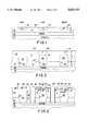
- FIGS. 1, 2, and 3are partial vertical cross sections of an embodiment of the present invention illustrating stages in the manufacture thereof.
- FIG. 4is a cutaway view of an embodiment of a JFET of the present invention illustrating an optional top gate alignment.
- FIG. 5is a cutaway view of a further embodiment of a JFET of the present invention illustrating an another top gate alignment, and another embodiment of the bottom gate and substrate.
- a semiconductor devicemay include complementary NPN and PNP transistors and a JFET.
- An N type JFETis shown, although a P type JFET may be provided instead of, or in addition to, the NJFET.
- An N or P type wafer 12may be attached (e.g., with a conventional oxide to oxide bond) to a handle wafer 14 overlain with an oxide layer 16.
- the thickness T1 of the wafer 12may be reduced as appropriate.
- Part of a more heavily doped buried layer for the NPN transistormay be implanted by patterning and doping a region 18 in joining surface 20.
- Parts of the more heavily doped lower (or back) collector layer for the PNP transistor, and of the bottom gate for the JFETmay be implanted by patterning and doping regions 22 and 24 in the same steps.
- the terms "front” and “back”respectively refer to the top and bottom of the semiconductor device as shown in the vertical cross section of FIG. 3.)
- the patterning and dopingmay be carried out conventionally.
- a layer 26may be epitaxially grown on joining surface 20.
- the thickness T2 and resistivity of the epitaxial layermay be set as appropriate.
- a front collector layer for the PNP transistor, and a bottom gate contact for the JFETmay be implanted into the top surface 28 of the epitaxial layer by patterning front collector layer 30 and front contact layer 32 in the same steps.
- the dopant from regions 18, 22, and 24is being up-diffused from the surface 20 into the epitaxial layer 26 to form NPN buried layer 34, PNP back collector layer 36, and JFET bottom gate 38.
- the up-diffusing region 24joins the down-diffusing front contact layer 32 to provide a contact for the JFET bottom gate 38 from the surface 28, and the up-diffusing region 22 joins the down-diffusing front collector layer 30 to form PNP collector 40 with more heavily doped back collector layer 36.
- the back collector layer 36 and the front collector layer 30should overlap for the entire range of thicknesses of the epitaxial layer 26, and yet the back collector should not be close enough to the top surface of the epitaxial layer to reduce breakdown voltage as discussed above.
- the front collector layer 30has an integrated doping of about 7 ⁇ 10 12 ions per square centimeter and a maximum concentration of about 1 ⁇ 10 16 ions per cubic centimeter at the epitaxial surface from which the diffusion is made
- the back collector layer 36has an integrated doping of about 3.5 ⁇ 10 13 ions per square centimeter and a maximum concentration of about 7 ⁇ 10 13 ions per cubic centimeter at the bottom of the epitaxial layer.
- the further elements of the transistors and the JFETmay be implanted into the surface 28.
- the P type base 42 for the NPN transistor and the N type base 44 for the PNPmay be patterned and doped.
- the P+ PNP emitter 46 and collector contact 48may be similarly provided.
- a top gate 50 for the JFETis preferably provided in the same steps when other elements of similar conductivity type are formed.
- the N+ source 52 and drain 54, N+ base contact 56 for the PNP, and the N+ emitter 58 and collector contact 60 for the NPNmay be patterned and doped, preferably in the same step.
- the PNP and NPN transistors and the JFETmay be electrically isolated as required. For example, they may isolated using conventional trenches 62 formed at any appropriate stage of the fabrication process after growth of the epitaxial layer 26, preferably before the front P diffusion of layers 30 and 32. Alternatively, they may be junction isolated using conventional methods (not shown).
- the pinch-off voltageis less than 5 volts and the breakdown voltage Bvceo is at least 30 volts.
- T1may be about 5 microns and T2 about 15 microns (14.75 microns ⁇ 5%).
- the doping concentration of the epitaxial layer 26may be about 1 ⁇ 10 15 ions per cubic centimeter, so that resistivity is about 4 ohm-centimeters ( ⁇ 10%).
- the up-diffusing more heavily doped back collector layer 36should not get closer than about 5.5 microns to the surface 28 (the PNP base 44 is desirably about 3 microns thick).
- the up-diffusing bottom gate 38should get no closer than about 5.1 microns to the surface 28 (distance D in FIG. 3). As these up-diffusions are desirably carried out in the same step, one of the distances will be effected. This conflict can be resolved by reducing the dopant concentration of the back collector layer 36 to about 3.5 ⁇ 10 13 ions per square centimeter and allowing the up-diffusing dopant to rise to 5.1 microns from surface 28. Assuming that the top gate 50 is about 1.5 microns thick, the JFET channel between the top gate 50 and the bottom gate 38 has a thickness t of about 3.65 microns.
- HFEmay be set to any desired value (e.g., 100 in the above-described embodiment) by controlling the active base doping of the PNP to the appropriate value using techniques known in the art.
- the trench isolation technique illustrated in FIG. 3is preferred when the dopant concentration is reduced to about 3.5 ⁇ 10 13 ions per square centimeter. Junction isolation techniques may need a higher dopant concentration (e.g., on the order of 1 ⁇ 10 15 ions per square centimeter) to suppress parasitic transistors that can cause latch up.
- the trench isolation and bottom oxide isolation illustratedeliminate the parasitic devices that can arise from the isolating PN junctions, thus eliminating latch up without constraining dopant concentration.
- an NPN transistorwith a more heavily doped buried layer 34 that is not as close to the base 42 as the back collector layer 36 is to the base 44 in the PNP transistor.
- a greater separationmay be needed in the NPN to achieve an acceptable breakdown voltage. This may be particularly difficult in the event a lower dopant concentration is used in the back collector layer 36 as a longer diffusion time will be needed.
- the up-diffusing distance of the buried layer 34may be reduced by using an N+ type dopant that has a lower diffusion coefficient than the P type dopant used in the back collector layer 36.
- the N+ type dopantmay be arsenic or antimony and the P type dopant may be boron.
- FIGS. 4 and 5several options for alignment of the JFET top gate are available. (The element numbers of FIGS. 1-3 have been used on similar elements in the interest of clarity.)
- the top gate 50overlaps the bottom gate contact 32 to tie the two gates together.
- the P+ top gate 50runs inside the P bottom gate contact 32 around the periphery of an NJFET to provide channel stopping to protect against MOS inversion of the surface of the contact 32.
- the top gate 50is isolated from the bottom gate 38 so that the two gates may be independently biased.
- the top gate 50surrounds source 52 and drain 54 so that there is no path from either that does not pass between top and bottom gates.
- a P+ bottom gate contact region 64 in the contact 32, and an N+ channel stop ring 66 between the top gate 50 and the bottom gate contact 32may be provided.
- a junction isolated, non-bonded processmay be used with a P type substrate.
- an N isolation layer 68may be diffused into a P substrate 70 prior to growth of the epitaxial layer 26.
- the region 24 and JFET bottom gate 38may be formed as discussed above.
- the characteristics of the JFETmay be modified to optimize parameters for a particular application. This may be useful when several JFETs with different characteristics are to be provided.
- the doping of the bottom gatemay be more tightly controlled by setting the doping with a non-selective P type implant before the NPN N+ buried layer and PNP back collector layer are formed.
- the non-selective P type dopantshould have a low enough doping level (e.g., 1-2 ⁇ 10 12 ions per square centimeter) so that it does not convert the subsequently formed N+ buried layer to P type and so that it does not change the doping profile of the upper part of the back collector layer after it has been up-diffused.
- the bottom gate of the JFETmay be formed in a special diffusion step optimized to make the bottom gate, or the bottom gate diffusion may be avoided if the wafer 12 is P type.
Landscapes
- Junction Field-Effect Transistors (AREA)
- Bipolar Integrated Circuits (AREA)
Abstract
Description
Vp={[qN.sub.D (0.5t).sup.2 ]/(2ε.sub.SI ε.sub.0)}-Φ.sub.B ( 1)Claims (27)
Priority Applications (1)
| Application Number | Priority Date | Filing Date | Title |
|---|---|---|---|
| US08/543,754US5652153A (en) | 1994-07-22 | 1995-10-16 | Method of making JFET structures for semiconductor devices with complementary bipolar transistors |
Applications Claiming Priority (2)
| Application Number | Priority Date | Filing Date | Title |
|---|---|---|---|
| US27902494A | 1994-07-22 | 1994-07-22 | |
| US08/543,754US5652153A (en) | 1994-07-22 | 1995-10-16 | Method of making JFET structures for semiconductor devices with complementary bipolar transistors |
Related Parent Applications (1)
| Application Number | Title | Priority Date | Filing Date |
|---|---|---|---|
| US27902494AContinuation | 1994-07-22 | 1994-07-22 |
Publications (1)
| Publication Number | Publication Date |
|---|---|
| US5652153Atrue US5652153A (en) | 1997-07-29 |
Family
ID=23067356
Family Applications (1)
| Application Number | Title | Priority Date | Filing Date |
|---|---|---|---|
| US08/543,754Expired - LifetimeUS5652153A (en) | 1994-07-22 | 1995-10-16 | Method of making JFET structures for semiconductor devices with complementary bipolar transistors |
Country Status (1)
| Country | Link |
|---|---|
| US (1) | US5652153A (en) |
Cited By (6)
| Publication number | Priority date | Publication date | Assignee | Title |
|---|---|---|---|---|
| US6271070B2 (en)* | 1997-12-25 | 2001-08-07 | Matsushita Electronics Corporation | Method of manufacturing semiconductor device |
| US20030162360A1 (en)* | 2002-02-25 | 2003-08-28 | Beasom James D. | Reduced mask count buried layer process |
| US6624497B2 (en)* | 2002-02-25 | 2003-09-23 | Intersil Americas, Inc | Semiconductor device with a reduced mask count buried layer |
| DE102004051081A1 (en)* | 2004-10-19 | 2006-04-27 | Austriamicrosystems Ag | JFET and manufacturing process |
| US20080036009A1 (en)* | 2006-08-10 | 2008-02-14 | Vora Madhukar B | JFET with built in back gate in either SOI or bulk silicon |
| US20110286135A1 (en)* | 2010-05-18 | 2011-11-24 | International Business Machines Corporation | Silicon Controlled Rectifier Based Electrostatic Discharge Protection Circuit With Integrated JFETS, Method Of Operation And Design Structure |
Citations (6)
| Publication number | Priority date | Publication date | Assignee | Title |
|---|---|---|---|---|
| US4403395A (en)* | 1979-02-15 | 1983-09-13 | Texas Instruments Incorporated | Monolithic integration of logic, control and high voltage interface circuitry |
| US4553318A (en)* | 1983-05-02 | 1985-11-19 | Rca Corporation | Method of making integrated PNP and NPN bipolar transistors and junction field effect transistor |
| US4729008A (en)* | 1982-12-08 | 1988-03-01 | Harris Corporation | High voltage IC bipolar transistors operable to BVCBO and method of fabrication |
| US4939099A (en)* | 1988-06-21 | 1990-07-03 | Texas Instruments Incorporated | Process for fabricating isolated vertical bipolar and JFET transistors |
| US5151765A (en)* | 1988-05-20 | 1992-09-29 | Fujitsu Limited | Semiconductor device comprising high-speed and high-current transistors formed in a common substrate and having matched characteristics |
| US5296409A (en)* | 1992-05-08 | 1994-03-22 | National Semiconductor Corporation | Method of making n-channel and p-channel junction field-effect transistors and CMOS transistors using a CMOS or bipolar/CMOS process |
- 1995
- 1995-10-16USUS08/543,754patent/US5652153A/ennot_activeExpired - Lifetime
Patent Citations (6)
| Publication number | Priority date | Publication date | Assignee | Title |
|---|---|---|---|---|
| US4403395A (en)* | 1979-02-15 | 1983-09-13 | Texas Instruments Incorporated | Monolithic integration of logic, control and high voltage interface circuitry |
| US4729008A (en)* | 1982-12-08 | 1988-03-01 | Harris Corporation | High voltage IC bipolar transistors operable to BVCBO and method of fabrication |
| US4553318A (en)* | 1983-05-02 | 1985-11-19 | Rca Corporation | Method of making integrated PNP and NPN bipolar transistors and junction field effect transistor |
| US5151765A (en)* | 1988-05-20 | 1992-09-29 | Fujitsu Limited | Semiconductor device comprising high-speed and high-current transistors formed in a common substrate and having matched characteristics |
| US4939099A (en)* | 1988-06-21 | 1990-07-03 | Texas Instruments Incorporated | Process for fabricating isolated vertical bipolar and JFET transistors |
| US5296409A (en)* | 1992-05-08 | 1994-03-22 | National Semiconductor Corporation | Method of making n-channel and p-channel junction field-effect transistors and CMOS transistors using a CMOS or bipolar/CMOS process |
Cited By (14)
| Publication number | Priority date | Publication date | Assignee | Title |
|---|---|---|---|---|
| US6271070B2 (en)* | 1997-12-25 | 2001-08-07 | Matsushita Electronics Corporation | Method of manufacturing semiconductor device |
| USRE41477E1 (en) | 2002-02-25 | 2010-08-10 | Beasom James D | Semiconductor device with a reduced mask count buried layer |
| US20030162360A1 (en)* | 2002-02-25 | 2003-08-28 | Beasom James D. | Reduced mask count buried layer process |
| US6624497B2 (en)* | 2002-02-25 | 2003-09-23 | Intersil Americas, Inc | Semiconductor device with a reduced mask count buried layer |
| US20040171229A1 (en)* | 2002-02-25 | 2004-09-02 | Beasom James D. | Reduced mask count buried layer process |
| US6979624B2 (en) | 2002-02-25 | 2005-12-27 | Intersil Americas Inc. | Reduced mask count buried layer process |
| DE102004051081A1 (en)* | 2004-10-19 | 2006-04-27 | Austriamicrosystems Ag | JFET and manufacturing process |
| US20080036009A1 (en)* | 2006-08-10 | 2008-02-14 | Vora Madhukar B | JFET with built in back gate in either SOI or bulk silicon |
| US20090075435A1 (en)* | 2006-08-10 | 2009-03-19 | Dsm Solutions, Inc. | JFET With Built In Back Gate in Either SOI or Bulk Silicon |
| US7557393B2 (en) | 2006-08-10 | 2009-07-07 | Dsm Solutions, Inc. | JFET with built in back gate in either SOI or bulk silicon |
| US7645654B2 (en) | 2006-08-10 | 2010-01-12 | Dsm Solutions, Inc. | JFET with built in back gate in either SOI or bulk silicon |
| WO2008021919A1 (en)* | 2006-08-10 | 2008-02-21 | Dsm Solutions, Inc. | Jfet with built in back gate in either soi or bulk silicon |
| US20110286135A1 (en)* | 2010-05-18 | 2011-11-24 | International Business Machines Corporation | Silicon Controlled Rectifier Based Electrostatic Discharge Protection Circuit With Integrated JFETS, Method Of Operation And Design Structure |
| US8634172B2 (en)* | 2010-05-18 | 2014-01-21 | International Business Machines Corporation | Silicon controlled rectifier based electrostatic discharge protection circuit with integrated JFETs, method of operation and design structure |
Similar Documents
| Publication | Publication Date | Title |
|---|---|---|
| US4403395A (en) | Monolithic integration of logic, control and high voltage interface circuitry | |
| US5294823A (en) | SOI BICMOS process | |
| US4325180A (en) | Process for monolithic integration of logic, control, and high voltage interface circuitry | |
| US5034337A (en) | Method of making an integrated circuit that combines multi-epitaxial power transistors with logic/analog devices | |
| US4826780A (en) | Method of making bipolar transistors | |
| EP0591672B1 (en) | Method for fabricating bipolar junction and MOS transistors on SOI | |
| US4546370A (en) | Monolithic integration of logic, control and high voltage interface circuitry | |
| US5087580A (en) | Self-aligned bipolar transistor structure and fabrication process | |
| US7135364B2 (en) | Method of fabricating semiconductor integrated circuit | |
| US5218228A (en) | High voltage MOS transistors with reduced parasitic current gain | |
| US5565701A (en) | Integrated circuit with vertical bipolar power transistors and isolated lateral bipolar control transistors | |
| US20040207046A1 (en) | Integrated process for high voltage and high performance silicon-on-insulator bipolar devices | |
| JPH0315346B2 (en) | ||
| US5132235A (en) | Method for fabricating a high voltage MOS transistor | |
| JPH07297294A (en) | High-voltage P-channel metal oxide semiconductor device manufacturing method and high-voltage P-channel metal oxide semiconductor device | |
| US20050067631A1 (en) | Low noise vertical variable gate control voltage JFET device in a BiCMOS process and methods to build this device | |
| US5049513A (en) | Bi CMOS/SOI process flow | |
| EP0500233A2 (en) | Bipolar transistor structure & BICMOS IC fabrication process | |
| US6987309B2 (en) | Semiconductor device applied to a variable capacitance capacitor and amplifier | |
| US5652153A (en) | Method of making JFET structures for semiconductor devices with complementary bipolar transistors | |
| US5837590A (en) | Isolated vertical PNP transistor without required buried layer | |
| EP4070384A1 (en) | A transistor device | |
| US5302848A (en) | Integrated circuit with complementary junction-isolated bipolar transistors | |
| US5065214A (en) | Integrated circuit with complementary junction-isolated bipolar transistors | |
| EP0792514B1 (en) | Method of making an integrated circuit with complementary isolated bipolar transitors |
Legal Events
| Date | Code | Title | Description |
|---|---|---|---|
| STCF | Information on status: patent grant | Free format text:PATENTED CASE | |
| AS | Assignment | Owner name:INTERSIL CORPORATION, FLORIDA Free format text:ASSIGNMENT OF ASSIGNORS INTEREST;ASSIGNOR:HARRIS CORPORATION;REEL/FRAME:010247/0043 Effective date:19990813 | |
| AS | Assignment | Owner name:CREDIT SUISSE FIRST BOSTON, AS COLLATERAL AGENT, N Free format text:SECURITY INTEREST;ASSIGNOR:INTERSIL CORPORATION;REEL/FRAME:010351/0410 Effective date:19990813 | |
| FPAY | Fee payment | Year of fee payment:4 | |
| FPAY | Fee payment | Year of fee payment:8 | |
| FPAY | Fee payment | Year of fee payment:12 | |
| AS | Assignment | Owner name:MORGAN STANLEY & CO. INCORPORATED,NEW YORK Free format text:SECURITY AGREEMENT;ASSIGNORS:INTERSIL CORPORATION;TECHWELL, INC.;INTERSIL COMMUNICATIONS, INC.;AND OTHERS;REEL/FRAME:024390/0608 Effective date:20100427 | |
| AS | Assignment | Owner name:INTERSIL CORPORATION,FLORIDA Free format text:RELEASE BY SECURED PARTY;ASSIGNOR:CREDIT SUISSE FIRST BOSTON;REEL/FRAME:024445/0049 Effective date:20030306 |