US5651035A - Apparatus for reducing jitter of a spectrum spread clock signal and method therefor - Google Patents
Apparatus for reducing jitter of a spectrum spread clock signal and method thereforDownload PDFInfo
- Publication number
- US5651035A US5651035AUS08/430,575US43057595AUS5651035AUS 5651035 AUS5651035 AUS 5651035AUS 43057595 AUS43057595 AUS 43057595AUS 5651035 AUS5651035 AUS 5651035A
- Authority
- US
- United States
- Prior art keywords
- reference clock
- sub
- input
- pulses
- accumulator
- Prior art date
- Legal status (The legal status is an assumption and is not a legal conclusion. Google has not performed a legal analysis and makes no representation as to the accuracy of the status listed.)
- Expired - Fee Related
Links
- 238000001228spectrumMethods0.000titleclaimsabstractdescription29
- 238000000034methodMethods0.000titledescription8
- 230000004044responseEffects0.000claimsabstractdescription21
- 230000008859changeEffects0.000description4
- 239000003990capacitorSubstances0.000description3
- 230000003247decreasing effectEffects0.000description3
- 238000010586diagramMethods0.000description3
- 238000006073displacement reactionMethods0.000description2
- 230000008878couplingEffects0.000description1
- 238000010168coupling processMethods0.000description1
- 238000005859coupling reactionMethods0.000description1
- 230000005670electromagnetic radiationEffects0.000description1
- 230000005855radiationEffects0.000description1
- 230000007704transitionEffects0.000description1
Images


Classifications
- H—ELECTRICITY
- H03—ELECTRONIC CIRCUITRY
- H03L—AUTOMATIC CONTROL, STARTING, SYNCHRONISATION OR STABILISATION OF GENERATORS OF ELECTRONIC OSCILLATIONS OR PULSES
- H03L7/00—Automatic control of frequency or phase; Synchronisation
- H03L7/06—Automatic control of frequency or phase; Synchronisation using a reference signal applied to a frequency- or phase-locked loop
- H03L7/16—Indirect frequency synthesis, i.e. generating a desired one of a number of predetermined frequencies using a frequency- or phase-locked loop
- H03L7/18—Indirect frequency synthesis, i.e. generating a desired one of a number of predetermined frequencies using a frequency- or phase-locked loop using a frequency divider or counter in the loop
- H03L7/1806—Indirect frequency synthesis, i.e. generating a desired one of a number of predetermined frequencies using a frequency- or phase-locked loop using a frequency divider or counter in the loop the frequency divider comprising a phase accumulator generating the frequency divided signal
Definitions
- This inventionis in the field of clock pulse generation for a digital machine and methods therefore and, more particularly, is an apparatus for generating a substantially jitter free spectrum spread clock signal and method therefor.
- the average amplitude of the spectrum of undesired radiation caused by clock pulses in a digital computeris reduced when the frequency of the clock pulses continuously deviates from a center frequency.
- the clock pulses with the continuously deviating frequencyare generated by a spectrum spread clock.
- Spectrum spread clock pulsesare generated by providing a digital signal representation of an input angle to a circuit arrangement that includes a type of digital storage device known as an accumulator.
- the accumulatoris connected to a reference clock pulse generator.
- the accumulatorhas an output that provides a digital signal representation of an accumulated angle which is incremented by the input angle in response to a reference clock pulse.
- the output of the accumulatoris connected to a programmable read only memory (PROM) at its input.
- PROMprogrammable read only memory
- the PROMprovides a digital signal representation of the sine of the accumulated angle.
- the output of the PROMis connected to a digital to analog converter (D/A) that drives a squaring circuit which provides input pulses to a phase locked loop.
- the input pulsesare at a frequency directly related to the input angle.
- the phase locked loopprovides the spectrum spread clock pulses.
- the circuit arrangement described hereinbeforeis suitable for generating the spectrum spread clock pulses, it is costly because of the number of circuit components included therein.
- the PROM, the D/A, the low pass filter and the squaring circuitare eliminated.
- the phase locked loopis driven by the most significant bit (MSB) of the output of the accumulator.
- the MSBundergoes a transition from a logic "1" signal to a logic “0" signal or vice versa
- the accumulated angletypically changes by more than an angle represented by a least significant bit (LSB) of the accumulator.
- LSBleast significant bit
- the jitter of the MSBis reduced by increasing the frequency of the reference clock and decreasing the input angle.
- An object of the present inventionis an apparatus and a method of reducing undesired coupling of a clock pulse via electromagnetic radiation and method therefor.
- Another object of the present inventionis an apparatus and a method for utilizing signal processing at a reduced frequency to generate spectrum spread clock pulses.
- Another object of the present inventionis an apparatus and a method for economically generating jitter free spectrum spread clock pulses.
- an accumulatorstores a digital signal representation of an accumulated angle that is incremented by an input angle in response to a reference clock pulse.
- Spectrum spread clock pulsesare provided by a phase locked loop in response to a signal representation of the most significant bit of the accumulated angle.
- a compensation networkinjects a current into a loop filter of the phase locked loop to compensate for current injected into the loop filter during an overshoot interval.
- the present inventionprovides an apparatus and a method for economically generating jitter free spectrum spread clock pulses. Moreover, the spectrum spread clock pulses are generated in response to signals derived from a clock source that generates reference clock pulses at a frequency much lower than frequencies of a circuit arrangement in accordance with the prior art.
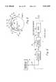
- FIG. 1is a block diagram of a circuit arrangement for generating spectrum spread clock pulses in accordance with the prior art.
- FIG. 2is a schematic block diagram of the preferred embodiment of the present invention.
- FIG. 3is a graphic representation of the phases of signals in the embodiment of FIG. 1;
- FIG. 4is a block diagram of an input angle signal generator in the embodiment of FIG. 2.
- a well known circuit arrangement for generating spectrum spread clock pulsesincludes an accumulator 10 that has an input where a digital signal representation of an input angle is provided through a plurality of signal lines 12 by an input angle signal generator 14. Accumulator 10 is additionally connected through a signal line 15 to a reference clock pulse generator 16 whereby reference clock pulses are provided to accumulator 10.
- Reference clock 16is additionally connected to input angle generator 14 through line 15 whereby reference clock pulses are provided to input angle generator 14. The input angle signals are generated in response to the reference clock pulses.
- Accumulator 10stores a digital signal representation of an accumulated angle.
- the output of accumulator 10is the signal representation of the accumulated angle.
- the accumulated angleis in accordance with a relationship which is given as: ##EQU1##
- M iis the input angle
- Kis the state size of accumulator 10.
- nis the number of binary bits stored by accumulator 10.
- the accumulated angleis zero.
- the accumulated angleis equal to the input angle.
- the accumulated angleis incrementally increased in response to a reference clock pulse. Moreover, the increase equals the input angle.
- Accumulator 10is connected through a plurality of signal lines 18 to the input of a programmable read only memory 20 (referred to hereinafter as PROM 20).
- PROM 20In response to the signal representation of the accumulated angle, PROM 20 provides at its output a digital signal representation of the sine of the accumulated angle.
- the output of PROM 20is connected through a plurality of signal lines 22 to inputs of a digital to analog converter 24 (referred to hereinafter as D/A 24).
- D/A 24In response to the digital signal representation of the sine of the accumulated angle, D/A 24 provides at its output a voltage that is an analog signal representation of the sine of the accumulated angle.
- the output of D/A 24provides successive voltages that are respectively representative of successive points along a sinusoid.
- the output of D/A 24is connected through a signal line 26 to the input of a low pass filter 28.
- Filter 28provides an output that is substantially an interpolation between the successive voltages that are provided by D/A 24. Accordingly, the output of filter 28 is a substantially sinusoidal voltage.
- the output of filter 28is connected through a signal line 30 to the input of a squaring circuit 32 of any suitable type.
- Circuit 32provides at its output a voltage having a square waveform in response to a sinusoidal input voltage.
- Squaring circuitssuch as a Schmitt trigger, are well known to those skilled in the art.
- phase locked loop 36that provides the spectrum spread clock pulses.
- Phase locked loopsare well known to those skilled in the art.
- circuit arrangement described hereinbeforeis suitable for providing the spectrum spread clock pulses, it is expensive and unreliable because it includes components such as PROM 20, D/A 24, filter 28 and squaring circuit 32; these are not included in the preferred embodiment.
- phase locked loop 36includes a phase detector 38 with inputs 40, 42 where pulses are compared.
- phase detector 38provides an output current of a known polarity.
- the output currentis of a polarity opposite from the known polarity.
- phase detector 38does not provide current.
- phase locked loopis locked, either logic "0” or logic "1” are simultaneously provided at inputs to its phase detector.
- phase detector 38The output of phase detector 38 is connected through a loop filter 44 to ground.
- Loop filter 44is comprised of a capacitor 46 connected in series with a resistor 48. Because phase detector 38 provides current as described hereinbefore, phase detector 38 is operable to either charge or discharge capacitor 46 or maintain a charge thereon unchanged.
- Loop filter 44is connected to a voltage controlled oscillator 50 (referred to hereinafter as VCO 50) whereby loop filter 44 substantially provides a voltage stored on capacitor 46 to VCO 50.
- VCO 50provides spectrum spread clock pulses at a spectrum spread clock frequency proportional to the voltage provided by loop filter 44.
- VCO 50The output of VCO 50 is connected through a signal line 52 to the input of a frequency divider 54.
- Divider 54provides pulses at a frequency which is a submultiple of the spectrum spread clock frequency.
- the output of divider 54is connected to input 42.
- a salient feature of the present inventionrelates to compensating for logic "0" being provided at input 40 during the overshoot interval.
- the most significant bit of the output of accumulator 10is connected through a signal line 56 to input 40, whereby phase detector 38 is driven by a signal representation of the most significant bit (MSB) of the accumulated angle. From the input relationship given hereinbefore (equation 1), when the input angle is increased, the MSB provides pulses at an increased frequency because the state size, K, is finite.
- phase locked loop 36Since phase locked loop 36 is locked, the frequency of the MSB pulses and the frequency of pulses provided by divider 54 are identical and the spectrum spread clock frequency is correspondingly increased. In a similar manner, when the input angle is decreased, the spectrum spread clock frequency is decreased.
- a semicircular arc 58is representative of when divider 54 provides logic "0". More particularly, time is measured by an angular displacement in a clockwise direction along arc 58. At a time represented by a location 60 on arc 58, there is an intersection between arc 58 and a datum line 62 when a pulse provided by VCO 50 causes the output of divider 54 to change from logic "0" to logic "1".
- an arc 64is representative of when the MSB is logic "0". Arc 64 is concentric with arc 58.
- a reference clock pulsecauses a jump change to a time represented by location 68 on arc 64.
- the angular displacement of location 66 from location 68is a representation of the period of reference clock 16.
- the jump change from location 66 to location 68is represented as taking place along an arc 70 in the direction of an arrow 72 for clarity.
- jump changes caused by reference clock pulsesare represented as taking place along arcs 73, 74, 75 to locations 76, 77, 78 on arc 64, respectively. It should be understood that the number of jump changes is inversely related to the input angle.
- a reference clock pulsecauses the MSB to change from logic “0" to logic "1".
- An arc segment 80extends from datum line 62 to location 78. Since the output of divider 54 changes from logic “0" to logic “1” at the time represented by location 60, arc segment 80 is representative of an overshoot interval during which divider 54 provides logic “1” and the MSB is logic "0". Without compensation for the overshoot interval, there is jitter in the spectrum spread clock pulses.
- ⁇ Tis the overshoot interval
- T cis the period of reference clock 26
- GP-K/2 immediately after the MSB changes from logic "0" to logic "1".
- the lower order bits stored in accumulator 10are a binary signal representation of the quantity, G.
- a chargeis injected into loop filter 44 during the overshoot interval in accordance with a relationship which is given as:
- phase detector 18is current provided by phase detector 18 during the overshoot interval.
- a compensating chargeis removed from loop filter 44 during an interval equal to an integral number of periods of reference clock 16.
- the charge removalcompensates for the charge injected into loop filter 44 during the overshoot interval.
- the compensating chargeis removed when a current is provided to loop filter 44 in accordance with the following relationship:
- Q xis the compensating charge removed from loop filter 44
- i xis a current provided to loop filter 44 to cause the removal of the compensating charge, Q x ;
- mis the number of periods of reference clock 16 during which the compensating charge is removed.
- a compensation network 82(FIG. 2) has inputs connected to accumulator 10 through line 56 and a plurality of signal lines 84, whereby the signal representation of the accumulated angle is provided to network 82. Additionally, network 82 is connected to reference clock 16 and input angle generator 14 through line 15 and lines 12, respectively. The output of network 82 is connected to loop filter 44.
- Network 82includes a storage register that stores the lower order bits stored in accumulator 10 and the input angle signals when the MSB changes from logic "0" to logic "1". Storage registers are well known to those skilled in the art.
- Network 82additionally includes a timing circuit that provides logic "1” in response to a first reference clock pulse after the MSB is logic “1” and provides logic “0” in response to a second reference clock pulse. Accordingly, the timing circuit provides logic "1" for a one period interval of reference clock 16.
- the storage register and the output of the timing circuitare connected to inputs of a read only memory that is programmed to provide a digital signal representation of the current, i x , during the one period interval and provide a signal representation of zero at all other times.
- the output of the read only memoryis connected to a digitally controlled current source that provides the current, i x .
- Digitally controlled current sourcesare well known to those skilled in the art.
- input angle generator 14includes a frequency divider 86 that has its input connected through line 15 to reference clock 16. In response to the reference clock pulses, divider 86 provides reference divider pulses at a frequency that is a submultiple of the reference clock frequency.
- Counter 90is of a well known type that provides address signals that are a digital signal representation of a binary address number which is incremented in response to a reference divider pulse.
- the address signalsare sequentially provided at a frequency which is a submultiple of the reference clock frequency. It should be understood that when the address number is a maximum, a reference divider pulse causes counter 90 to overflow and store a signal representation of zero.
- PROM 94programmable read only memory 94
- VCO 50FPGA 50
Landscapes
- Stabilization Of Oscillater, Synchronisation, Frequency Synthesizers (AREA)
Abstract
Description
ΔT=[GT.sub.c ]/M (2)
Q.sub.os =(i.sub.pd GT.sub.c)/M (3)
Q.sub.x =i.sub.x (mT.sub.c)=Q.sub.os (4)
Claims (5)
ΔT=[GT.sub.c ]/M
Q.sub.os =(i.sub.pd GT.sub.c)/M
Q.sub.x =i.sub.x (mT.sub.c)=Q.sub.os
i.sub.x =i.sub.pd G/mM.
Priority Applications (1)
| Application Number | Priority Date | Filing Date | Title |
|---|---|---|---|
| US08/430,575US5651035A (en) | 1995-04-28 | 1995-04-28 | Apparatus for reducing jitter of a spectrum spread clock signal and method therefor |
Applications Claiming Priority (1)
| Application Number | Priority Date | Filing Date | Title |
|---|---|---|---|
| US08/430,575US5651035A (en) | 1995-04-28 | 1995-04-28 | Apparatus for reducing jitter of a spectrum spread clock signal and method therefor |
Publications (1)
| Publication Number | Publication Date |
|---|---|
| US5651035Atrue US5651035A (en) | 1997-07-22 |
Family
ID=23708142
Family Applications (1)
| Application Number | Title | Priority Date | Filing Date |
|---|---|---|---|
| US08/430,575Expired - Fee RelatedUS5651035A (en) | 1995-04-28 | 1995-04-28 | Apparatus for reducing jitter of a spectrum spread clock signal and method therefor |
Country Status (1)
| Country | Link |
|---|---|
| US (1) | US5651035A (en) |
Cited By (62)
| Publication number | Priority date | Publication date | Assignee | Title |
|---|---|---|---|---|
| WO1998057420A1 (en)* | 1997-06-13 | 1998-12-17 | Integrated Circuit Systems, Inc. | Apparatus and method for controlling spectrum of a signal |
| US6016069A (en)* | 1998-02-10 | 2000-01-18 | Ericsson Inc. | Attenuating systems and methods for acquiring synchronization in phase locked loops |
| WO2000038344A1 (en)* | 1998-12-18 | 2000-06-29 | Koninklijke Philips Electronics N.V. | Compensation for phase errors caused by clock jitter in a cdma communication system |
| US6141394A (en)* | 1997-12-22 | 2000-10-31 | Philips Electronics North America Corporation | Fractional-N frequency synthesizer with jitter compensation |
| US6294936B1 (en) | 1998-09-28 | 2001-09-25 | American Microsystems, Inc. | Spread-spectrum modulation methods and circuit for clock generator phase-locked loop |
| US6330296B1 (en) | 1998-06-12 | 2001-12-11 | International Business Machines Corporation | Delay-locked loop which includes a monitor to allow for proper alignment of signals |
| WO2002005431A1 (en)* | 2000-07-10 | 2002-01-17 | Ciena Corporation | Frequency synthesizer |
| US6366174B1 (en) | 2000-02-21 | 2002-04-02 | Lexmark International, Inc. | Method and apparatus for providing a clock generation circuit for digitally controlled frequency or spread spectrum clocking |
| US6463110B1 (en) | 2001-03-21 | 2002-10-08 | Motorola, Inc. | Timing synchronization in a communication device |
| US6639933B2 (en)* | 1997-01-30 | 2003-10-28 | Hitachi. Ltd. | Phase-locked loop circuit and radio communication apparatus using the same |
| US6658043B2 (en) | 2001-10-26 | 2003-12-02 | Lexmark International, Inc. | Method and apparatus for providing multiple spread spectrum clock generator circuits with overlapping output frequencies |
| US20050122145A1 (en)* | 2003-12-04 | 2005-06-09 | Fujitsu Limited | Clock generator |
| US20070001882A1 (en)* | 2005-07-01 | 2007-01-04 | Realtek Semiconductor Corp. | Method and circuit for producing spread spectrum and/or over clock signal |
| US7233183B1 (en) | 2003-02-27 | 2007-06-19 | Cypress Semiconductor Corporation | Wide frequency range DLL with dynamically determined VCDL/VCO operational states |
| US7295049B1 (en) | 2004-03-25 | 2007-11-13 | Cypress Semiconductor Corporation | Method and circuit for rapid alignment of signals |
| US7330078B1 (en)* | 2004-12-20 | 2008-02-12 | Cypress Semiconductor Corporation | Apparatus and method for limiting the overshoot and undershoot when turning on the spread spectrum of a reference signal |
| US7388440B1 (en) | 2003-12-05 | 2008-06-17 | Cypress Semiconductor Corp. | Circuit and method to speed up PLL lock-time and prohibit frequency runaway |
| US7432749B1 (en) | 2004-06-23 | 2008-10-07 | Cypress Semiconductor Corp. | Circuit and method for improving frequency range in a phase locked loop |
| US20090295435A1 (en)* | 2008-05-30 | 2009-12-03 | Motorola, Inc. | Method and apparatus for reducing spurs in a fractional-n synthesizer |
| US7761845B1 (en) | 2002-09-09 | 2010-07-20 | Cypress Semiconductor Corporation | Method for parameterizing a user module |
| US7765095B1 (en) | 2000-10-26 | 2010-07-27 | Cypress Semiconductor Corporation | Conditional branching in an in-circuit emulation system |
| US7770113B1 (en) | 2001-11-19 | 2010-08-03 | Cypress Semiconductor Corporation | System and method for dynamically generating a configuration datasheet |
| US7774190B1 (en) | 2001-11-19 | 2010-08-10 | Cypress Semiconductor Corporation | Sleep and stall in an in-circuit emulation system |
| US7813411B1 (en) | 2005-06-30 | 2010-10-12 | Cypress Semiconductor Corporation | Spread spectrum frequency synthesizer with high order accumulation for frequency profile generation |
| US7825688B1 (en) | 2000-10-26 | 2010-11-02 | Cypress Semiconductor Corporation | Programmable microcontroller architecture(mixed analog/digital) |
| US7844437B1 (en) | 2001-11-19 | 2010-11-30 | Cypress Semiconductor Corporation | System and method for performing next placements and pruning of disallowed placements for programming an integrated circuit |
| US7912109B1 (en) | 2005-06-30 | 2011-03-22 | Cypress Semiconductor Corporation | Spread spectrum frequency synthesizer with first order accumulation for frequency profile generation |
| US7932787B1 (en) | 2005-06-30 | 2011-04-26 | Cypress Semiconductor Corporation | Phase lock loop control system and method |
| US7948327B1 (en) | 2005-06-30 | 2011-05-24 | Cypress Semiconductor Corporation | Simplified phase lock loop control model system and method |
| US7961059B1 (en) | 2005-06-30 | 2011-06-14 | Cypress Semiconductor Corporation | Phase lock loop control system and method with non-consecutive feedback divide values |
| US8019299B1 (en) | 2004-06-25 | 2011-09-13 | Cypress Semiconductor Corporation | Radio communication device and method |
| US8026739B2 (en) | 2007-04-17 | 2011-09-27 | Cypress Semiconductor Corporation | System level interconnect with programmable switching |
| US8040266B2 (en) | 2007-04-17 | 2011-10-18 | Cypress Semiconductor Corporation | Programmable sigma-delta analog-to-digital converter |
| US8049569B1 (en) | 2007-09-05 | 2011-11-01 | Cypress Semiconductor Corporation | Circuit and method for improving the accuracy of a crystal-less oscillator having dual-frequency modes |
| US8069428B1 (en) | 2001-10-24 | 2011-11-29 | Cypress Semiconductor Corporation | Techniques for generating microcontroller configuration information |
| US8067948B2 (en) | 2006-03-27 | 2011-11-29 | Cypress Semiconductor Corporation | Input/output multiplexer bus |
| US8069405B1 (en) | 2001-11-19 | 2011-11-29 | Cypress Semiconductor Corporation | User interface for efficiently browsing an electronic document using data-driven tabs |
| US8069436B2 (en) | 2004-08-13 | 2011-11-29 | Cypress Semiconductor Corporation | Providing hardware independence to automate code generation of processing device firmware |
| US8072277B1 (en) | 2005-06-30 | 2011-12-06 | Cypress Semiconductor Corporation | Spread spectrum frequency synthesizer |
| US8078894B1 (en) | 2007-04-25 | 2011-12-13 | Cypress Semiconductor Corporation | Power management architecture, method and configuration system |
| US8078970B1 (en) | 2001-11-09 | 2011-12-13 | Cypress Semiconductor Corporation | Graphical user interface with user-selectable list-box |
| US8085100B2 (en) | 2005-02-04 | 2011-12-27 | Cypress Semiconductor Corporation | Poly-phase frequency synthesis oscillator |
| US8085067B1 (en) | 2005-12-21 | 2011-12-27 | Cypress Semiconductor Corporation | Differential-to-single ended signal converter circuit and method |
| US8092083B2 (en) | 2007-04-17 | 2012-01-10 | Cypress Semiconductor Corporation | Temperature sensor with digital bandgap |
| US8103496B1 (en) | 2000-10-26 | 2012-01-24 | Cypress Semicondutor Corporation | Breakpoint control in an in-circuit emulation system |
| US8103497B1 (en) | 2002-03-28 | 2012-01-24 | Cypress Semiconductor Corporation | External interface for event architecture |
| US8120408B1 (en) | 2005-05-05 | 2012-02-21 | Cypress Semiconductor Corporation | Voltage controlled oscillator delay cell and method |
| US8130025B2 (en) | 2007-04-17 | 2012-03-06 | Cypress Semiconductor Corporation | Numerical band gap |
| US8149048B1 (en) | 2000-10-26 | 2012-04-03 | Cypress Semiconductor Corporation | Apparatus and method for programmable power management in a programmable analog circuit block |
| US8160864B1 (en) | 2000-10-26 | 2012-04-17 | Cypress Semiconductor Corporation | In-circuit emulator and pod synchronized boot |
| US8174326B1 (en) | 2005-06-30 | 2012-05-08 | Cypress Semiconductor Corporation | Phase lock loop control error selection system and method |
| US8176296B2 (en) | 2000-10-26 | 2012-05-08 | Cypress Semiconductor Corporation | Programmable microcontroller architecture |
| US8482313B2 (en) | 2007-04-17 | 2013-07-09 | Cypress Semiconductor Corporation | Universal digital block interconnection and channel routing |
| US8499270B1 (en) | 2007-04-25 | 2013-07-30 | Cypress Semiconductor Corporation | Configuration of programmable IC design elements |
| US8516025B2 (en) | 2007-04-17 | 2013-08-20 | Cypress Semiconductor Corporation | Clock driven dynamic datapath chaining |
| US8527949B1 (en) | 2001-11-19 | 2013-09-03 | Cypress Semiconductor Corporation | Graphical user interface for dynamically reconfiguring a programmable device |
| US20140327367A1 (en)* | 2010-06-03 | 2014-11-06 | Semiconductor Components Industries, Llc | Control circuit of light emitting element |
| US9448964B2 (en) | 2009-05-04 | 2016-09-20 | Cypress Semiconductor Corporation | Autonomous control in a programmable system |
| US9564902B2 (en) | 2007-04-17 | 2017-02-07 | Cypress Semiconductor Corporation | Dynamically configurable and re-configurable data path |
| US9720805B1 (en) | 2007-04-25 | 2017-08-01 | Cypress Semiconductor Corporation | System and method for controlling a target device |
| US10236897B1 (en)* | 2018-07-26 | 2019-03-19 | Texas Instruments Incorporated | Loss of lock detector |
| US10698662B2 (en) | 2001-11-15 | 2020-06-30 | Cypress Semiconductor Corporation | System providing automatic source code generation for personalization and parameterization of user modules |
Citations (4)
| Publication number | Priority date | Publication date | Assignee | Title |
|---|---|---|---|---|
| US5170297A (en)* | 1990-07-13 | 1992-12-08 | Standard Microsystems Corporation | Current averaging data separator |
| US5239561A (en)* | 1991-07-15 | 1993-08-24 | National Semiconductor Corporation | Phase error processor |
| US5285483A (en)* | 1992-04-07 | 1994-02-08 | Seiko Epson Corporation | Phase synchronization circuit |
| US5481563A (en)* | 1994-03-14 | 1996-01-02 | Network Systems Corporation | Jitter measurement using a statistically locked loop |
- 1995
- 1995-04-28USUS08/430,575patent/US5651035A/ennot_activeExpired - Fee Related
Patent Citations (4)
| Publication number | Priority date | Publication date | Assignee | Title |
|---|---|---|---|---|
| US5170297A (en)* | 1990-07-13 | 1992-12-08 | Standard Microsystems Corporation | Current averaging data separator |
| US5239561A (en)* | 1991-07-15 | 1993-08-24 | National Semiconductor Corporation | Phase error processor |
| US5285483A (en)* | 1992-04-07 | 1994-02-08 | Seiko Epson Corporation | Phase synchronization circuit |
| US5481563A (en)* | 1994-03-14 | 1996-01-02 | Network Systems Corporation | Jitter measurement using a statistically locked loop |
Cited By (86)
| Publication number | Priority date | Publication date | Assignee | Title |
|---|---|---|---|---|
| US20040032901A1 (en)* | 1997-01-30 | 2004-02-19 | Taizo Yamawaki | Phase-locked loop circuit and radio communication apparatus using the same |
| US6639933B2 (en)* | 1997-01-30 | 2003-10-28 | Hitachi. Ltd. | Phase-locked loop circuit and radio communication apparatus using the same |
| US7266171B2 (en) | 1997-01-30 | 2007-09-04 | Renesas Technology Corp. | Phase-locked loop circuit and radio communication apparatus using the same |
| US6046646A (en)* | 1997-06-13 | 2000-04-04 | Lo; Pedro W. | Modulation of a phase locked loop for spreading the spectrum of an output clock signal |
| WO1998057420A1 (en)* | 1997-06-13 | 1998-12-17 | Integrated Circuit Systems, Inc. | Apparatus and method for controlling spectrum of a signal |
| US6141394A (en)* | 1997-12-22 | 2000-10-31 | Philips Electronics North America Corporation | Fractional-N frequency synthesizer with jitter compensation |
| US6016069A (en)* | 1998-02-10 | 2000-01-18 | Ericsson Inc. | Attenuating systems and methods for acquiring synchronization in phase locked loops |
| US6330296B1 (en) | 1998-06-12 | 2001-12-11 | International Business Machines Corporation | Delay-locked loop which includes a monitor to allow for proper alignment of signals |
| US6294936B1 (en) | 1998-09-28 | 2001-09-25 | American Microsystems, Inc. | Spread-spectrum modulation methods and circuit for clock generator phase-locked loop |
| WO2000038344A1 (en)* | 1998-12-18 | 2000-06-29 | Koninklijke Philips Electronics N.V. | Compensation for phase errors caused by clock jitter in a cdma communication system |
| US6366174B1 (en) | 2000-02-21 | 2002-04-02 | Lexmark International, Inc. | Method and apparatus for providing a clock generation circuit for digitally controlled frequency or spread spectrum clocking |
| WO2002005431A1 (en)* | 2000-07-10 | 2002-01-17 | Ciena Corporation | Frequency synthesizer |
| US8736303B2 (en) | 2000-10-26 | 2014-05-27 | Cypress Semiconductor Corporation | PSOC architecture |
| US10261932B2 (en) | 2000-10-26 | 2019-04-16 | Cypress Semiconductor Corporation | Microcontroller programmable system on a chip |
| US9843327B1 (en) | 2000-10-26 | 2017-12-12 | Cypress Semiconductor Corporation | PSOC architecture |
| US10725954B2 (en) | 2000-10-26 | 2020-07-28 | Monterey Research, Llc | Microcontroller programmable system on a chip |
| US8149048B1 (en) | 2000-10-26 | 2012-04-03 | Cypress Semiconductor Corporation | Apparatus and method for programmable power management in a programmable analog circuit block |
| US8103496B1 (en) | 2000-10-26 | 2012-01-24 | Cypress Semicondutor Corporation | Breakpoint control in an in-circuit emulation system |
| US8160864B1 (en) | 2000-10-26 | 2012-04-17 | Cypress Semiconductor Corporation | In-circuit emulator and pod synchronized boot |
| US7825688B1 (en) | 2000-10-26 | 2010-11-02 | Cypress Semiconductor Corporation | Programmable microcontroller architecture(mixed analog/digital) |
| US8176296B2 (en) | 2000-10-26 | 2012-05-08 | Cypress Semiconductor Corporation | Programmable microcontroller architecture |
| US10020810B2 (en) | 2000-10-26 | 2018-07-10 | Cypress Semiconductor Corporation | PSoC architecture |
| US10248604B2 (en) | 2000-10-26 | 2019-04-02 | Cypress Semiconductor Corporation | Microcontroller programmable system on a chip |
| US9766650B2 (en) | 2000-10-26 | 2017-09-19 | Cypress Semiconductor Corporation | Microcontroller programmable system on a chip with programmable interconnect |
| US8358150B1 (en) | 2000-10-26 | 2013-01-22 | Cypress Semiconductor Corporation | Programmable microcontroller architecture(mixed analog/digital) |
| US7765095B1 (en) | 2000-10-26 | 2010-07-27 | Cypress Semiconductor Corporation | Conditional branching in an in-circuit emulation system |
| US8555032B2 (en) | 2000-10-26 | 2013-10-08 | Cypress Semiconductor Corporation | Microcontroller programmable system on a chip with programmable interconnect |
| US6463110B1 (en) | 2001-03-21 | 2002-10-08 | Motorola, Inc. | Timing synchronization in a communication device |
| US8069428B1 (en) | 2001-10-24 | 2011-11-29 | Cypress Semiconductor Corporation | Techniques for generating microcontroller configuration information |
| US10466980B2 (en) | 2001-10-24 | 2019-11-05 | Cypress Semiconductor Corporation | Techniques for generating microcontroller configuration information |
| US8793635B1 (en) | 2001-10-24 | 2014-07-29 | Cypress Semiconductor Corporation | Techniques for generating microcontroller configuration information |
| US6658043B2 (en) | 2001-10-26 | 2003-12-02 | Lexmark International, Inc. | Method and apparatus for providing multiple spread spectrum clock generator circuits with overlapping output frequencies |
| US8078970B1 (en) | 2001-11-09 | 2011-12-13 | Cypress Semiconductor Corporation | Graphical user interface with user-selectable list-box |
| US10698662B2 (en) | 2001-11-15 | 2020-06-30 | Cypress Semiconductor Corporation | System providing automatic source code generation for personalization and parameterization of user modules |
| US7844437B1 (en) | 2001-11-19 | 2010-11-30 | Cypress Semiconductor Corporation | System and method for performing next placements and pruning of disallowed placements for programming an integrated circuit |
| US7770113B1 (en) | 2001-11-19 | 2010-08-03 | Cypress Semiconductor Corporation | System and method for dynamically generating a configuration datasheet |
| US8069405B1 (en) | 2001-11-19 | 2011-11-29 | Cypress Semiconductor Corporation | User interface for efficiently browsing an electronic document using data-driven tabs |
| US7774190B1 (en) | 2001-11-19 | 2010-08-10 | Cypress Semiconductor Corporation | Sleep and stall in an in-circuit emulation system |
| US8533677B1 (en) | 2001-11-19 | 2013-09-10 | Cypress Semiconductor Corporation | Graphical user interface for dynamically reconfiguring a programmable device |
| US8527949B1 (en) | 2001-11-19 | 2013-09-03 | Cypress Semiconductor Corporation | Graphical user interface for dynamically reconfiguring a programmable device |
| US8370791B2 (en) | 2001-11-19 | 2013-02-05 | Cypress Semiconductor Corporation | System and method for performing next placements and pruning of disallowed placements for programming an integrated circuit |
| US8103497B1 (en) | 2002-03-28 | 2012-01-24 | Cypress Semiconductor Corporation | External interface for event architecture |
| US7761845B1 (en) | 2002-09-09 | 2010-07-20 | Cypress Semiconductor Corporation | Method for parameterizing a user module |
| US7233183B1 (en) | 2003-02-27 | 2007-06-19 | Cypress Semiconductor Corporation | Wide frequency range DLL with dynamically determined VCDL/VCO operational states |
| US20050122145A1 (en)* | 2003-12-04 | 2005-06-09 | Fujitsu Limited | Clock generator |
| US7098709B2 (en)* | 2003-12-04 | 2006-08-29 | Fujitsu Limited | Spread-spectrum clock generator |
| US7388440B1 (en) | 2003-12-05 | 2008-06-17 | Cypress Semiconductor Corp. | Circuit and method to speed up PLL lock-time and prohibit frequency runaway |
| US7893724B2 (en) | 2004-03-25 | 2011-02-22 | Cypress Semiconductor Corporation | Method and circuit for rapid alignment of signals |
| US7295049B1 (en) | 2004-03-25 | 2007-11-13 | Cypress Semiconductor Corporation | Method and circuit for rapid alignment of signals |
| US7432749B1 (en) | 2004-06-23 | 2008-10-07 | Cypress Semiconductor Corp. | Circuit and method for improving frequency range in a phase locked loop |
| US8019299B1 (en) | 2004-06-25 | 2011-09-13 | Cypress Semiconductor Corporation | Radio communication device and method |
| US8069436B2 (en) | 2004-08-13 | 2011-11-29 | Cypress Semiconductor Corporation | Providing hardware independence to automate code generation of processing device firmware |
| US7330078B1 (en)* | 2004-12-20 | 2008-02-12 | Cypress Semiconductor Corporation | Apparatus and method for limiting the overshoot and undershoot when turning on the spread spectrum of a reference signal |
| US8085100B2 (en) | 2005-02-04 | 2011-12-27 | Cypress Semiconductor Corporation | Poly-phase frequency synthesis oscillator |
| US8120408B1 (en) | 2005-05-05 | 2012-02-21 | Cypress Semiconductor Corporation | Voltage controlled oscillator delay cell and method |
| US8072277B1 (en) | 2005-06-30 | 2011-12-06 | Cypress Semiconductor Corporation | Spread spectrum frequency synthesizer |
| US8174326B1 (en) | 2005-06-30 | 2012-05-08 | Cypress Semiconductor Corporation | Phase lock loop control error selection system and method |
| US7813411B1 (en) | 2005-06-30 | 2010-10-12 | Cypress Semiconductor Corporation | Spread spectrum frequency synthesizer with high order accumulation for frequency profile generation |
| US7912109B1 (en) | 2005-06-30 | 2011-03-22 | Cypress Semiconductor Corporation | Spread spectrum frequency synthesizer with first order accumulation for frequency profile generation |
| US7932787B1 (en) | 2005-06-30 | 2011-04-26 | Cypress Semiconductor Corporation | Phase lock loop control system and method |
| US7948327B1 (en) | 2005-06-30 | 2011-05-24 | Cypress Semiconductor Corporation | Simplified phase lock loop control model system and method |
| US7961059B1 (en) | 2005-06-30 | 2011-06-14 | Cypress Semiconductor Corporation | Phase lock loop control system and method with non-consecutive feedback divide values |
| US20070001882A1 (en)* | 2005-07-01 | 2007-01-04 | Realtek Semiconductor Corp. | Method and circuit for producing spread spectrum and/or over clock signal |
| US7495496B2 (en)* | 2005-07-01 | 2009-02-24 | Realtek Semiconductor Corp. | Method and circuit for producing spread spectrum and/or over clock signal |
| US8085067B1 (en) | 2005-12-21 | 2011-12-27 | Cypress Semiconductor Corporation | Differential-to-single ended signal converter circuit and method |
| US8067948B2 (en) | 2006-03-27 | 2011-11-29 | Cypress Semiconductor Corporation | Input/output multiplexer bus |
| US8717042B1 (en) | 2006-03-27 | 2014-05-06 | Cypress Semiconductor Corporation | Input/output multiplexer bus |
| US9564902B2 (en) | 2007-04-17 | 2017-02-07 | Cypress Semiconductor Corporation | Dynamically configurable and re-configurable data path |
| US8040266B2 (en) | 2007-04-17 | 2011-10-18 | Cypress Semiconductor Corporation | Programmable sigma-delta analog-to-digital converter |
| US8516025B2 (en) | 2007-04-17 | 2013-08-20 | Cypress Semiconductor Corporation | Clock driven dynamic datapath chaining |
| US8130025B2 (en) | 2007-04-17 | 2012-03-06 | Cypress Semiconductor Corporation | Numerical band gap |
| US8092083B2 (en) | 2007-04-17 | 2012-01-10 | Cypress Semiconductor Corporation | Temperature sensor with digital bandgap |
| US8026739B2 (en) | 2007-04-17 | 2011-09-27 | Cypress Semiconductor Corporation | System level interconnect with programmable switching |
| US8482313B2 (en) | 2007-04-17 | 2013-07-09 | Cypress Semiconductor Corporation | Universal digital block interconnection and channel routing |
| US8476928B1 (en) | 2007-04-17 | 2013-07-02 | Cypress Semiconductor Corporation | System level interconnect with programmable switching |
| US8499270B1 (en) | 2007-04-25 | 2013-07-30 | Cypress Semiconductor Corporation | Configuration of programmable IC design elements |
| US8909960B1 (en) | 2007-04-25 | 2014-12-09 | Cypress Semiconductor Corporation | Power management architecture, method and configuration system |
| US8078894B1 (en) | 2007-04-25 | 2011-12-13 | Cypress Semiconductor Corporation | Power management architecture, method and configuration system |
| US9720805B1 (en) | 2007-04-25 | 2017-08-01 | Cypress Semiconductor Corporation | System and method for controlling a target device |
| US8049569B1 (en) | 2007-09-05 | 2011-11-01 | Cypress Semiconductor Corporation | Circuit and method for improving the accuracy of a crystal-less oscillator having dual-frequency modes |
| US7786772B2 (en)* | 2008-05-30 | 2010-08-31 | Motorola, Inc. | Method and apparatus for reducing spurs in a fractional-N synthesizer |
| US20090295435A1 (en)* | 2008-05-30 | 2009-12-03 | Motorola, Inc. | Method and apparatus for reducing spurs in a fractional-n synthesizer |
| US9448964B2 (en) | 2009-05-04 | 2016-09-20 | Cypress Semiconductor Corporation | Autonomous control in a programmable system |
| US9485817B2 (en)* | 2010-06-03 | 2016-11-01 | Semiconductor Components Industries, Llc | Control circuit of light emitting element |
| US20140327367A1 (en)* | 2010-06-03 | 2014-11-06 | Semiconductor Components Industries, Llc | Control circuit of light emitting element |
| US10236897B1 (en)* | 2018-07-26 | 2019-03-19 | Texas Instruments Incorporated | Loss of lock detector |
Similar Documents
| Publication | Publication Date | Title |
|---|---|---|
| US5651035A (en) | Apparatus for reducing jitter of a spectrum spread clock signal and method therefor | |
| US4780759A (en) | Sampling clock generation circuit of video signal | |
| US5959479A (en) | Sampling timebase system | |
| US5848047A (en) | Playback apparatus and playback method | |
| EP0168232A2 (en) | Apparatus for generating digital timing waveforms | |
| JPS5931897B2 (en) | frequency synthesizer | |
| US5247469A (en) | Digital frequency synthesizer and method with vernier interpolation | |
| JPH03253108A (en) | Direct digital synthesizer and signal generation | |
| US4972186A (en) | Resolver excitation circuit | |
| US6486743B2 (en) | Device for driving and detecting oscillator | |
| US4301415A (en) | Programmable multiple phase AC power supply | |
| US4417218A (en) | Linearizing circuit for a high frequency voltage controlled oscillator | |
| US4947382A (en) | Direct digital locked loop | |
| US6563350B1 (en) | Timing signal generator employing direct digital frequency synthesis | |
| US3599110A (en) | Self-clocking system having a variable frequency oscillator locked to leading edge of data and clock | |
| JPH0685633B2 (en) | Pole switch firing control circuit | |
| US4596964A (en) | Digital phase locked loop | |
| US4573024A (en) | PLL having two-frequency VCO | |
| JP2545008B2 (en) | Variable frequency signal generation method | |
| US4668923A (en) | Phase locked loop for locking an oscillator to a noninteger multiple of the reference frequency | |
| US5414391A (en) | Frequency synthesizer with frequency-division induced phase variation canceler | |
| US4464711A (en) | Gate pulse phase shifter | |
| JPS62188483A (en) | Error of time axis correcting device | |
| JP2780613B2 (en) | Frequency adjustment method of piezoelectric vibrator | |
| GB2160375A (en) | Phase controlled oscillator and a data demodulator including said oscillator |
Legal Events
| Date | Code | Title | Description |
|---|---|---|---|
| AS | Assignment | Owner name:INTERNATIONAL MICROCIRCUITS, INC., CALIFORNIA Free format text:ASSIGNMENT OF ASSIGNORS INTEREST;ASSIGNORS:TOZUN, ORHAN;MCCUNE, EARL WILLIAM JR.;REEL/FRAME:007480/0016 Effective date:19950412 | |
| AS | Assignment | Owner name:FLEET NATIONAL BANK, AS AGENT FOR ITSLEF AND EACH Free format text:CONDITIONAL PATENT COLLATERAL AGREEMENT;ASSIGNOR:INTERNATIONAL MICROCIRCUITS, INC.;REEL/FRAME:009197/0946 Effective date:19971216 | |
| FEPP | Fee payment procedure | Free format text:PAYOR NUMBER ASSIGNED (ORIGINAL EVENT CODE: ASPN); ENTITY STATUS OF PATENT OWNER: LARGE ENTITY | |
| FPAY | Fee payment | Year of fee payment:4 | |
| AS | Assignment | Owner name:INTERNATIONAL MICROCIRCUITS, INC., CALIFORNIA Free format text:RELEASE NUNC PRO TUNC;ASSIGNOR:FLEET NATIONAL BANK;REEL/FRAME:012280/0547 Effective date:20010605 | |
| FEPP | Fee payment procedure | Free format text:PAT HOLDER NO LONGER CLAIMS SMALL ENTITY STATUS, ENTITY STATUS SET TO UNDISCOUNTED (ORIGINAL EVENT CODE: STOL); ENTITY STATUS OF PATENT OWNER: LARGE ENTITY | |
| FPAY | Fee payment | Year of fee payment:8 | |
| AS | Assignment | Owner name:CYPRESS SEMICONDUCTOR CORPORATION, CALIFORNIA Free format text:ASSIGNMENT OF ASSIGNORS INTEREST;ASSIGNOR:INTERNATIONAL MICROSYSTEMS, INC.;REEL/FRAME:018323/0012 Effective date:20060928 | |
| REMI | Maintenance fee reminder mailed | ||
| LAPS | Lapse for failure to pay maintenance fees | ||
| STCH | Information on status: patent discontinuation | Free format text:PATENT EXPIRED DUE TO NONPAYMENT OF MAINTENANCE FEES UNDER 37 CFR 1.362 | |
| FP | Lapsed due to failure to pay maintenance fee | Effective date:20090722 |