US5650834A - Active-matrix device having silicide thin film resistor disposed between an input terminal and a short-circuit ring - Google Patents
Active-matrix device having silicide thin film resistor disposed between an input terminal and a short-circuit ringDownload PDFInfo
- Publication number
- US5650834A US5650834AUS08/363,030US36303094AUS5650834AUS 5650834 AUS5650834 AUS 5650834AUS 36303094 AUS36303094 AUS 36303094AUS 5650834 AUS5650834 AUS 5650834A
- Authority
- US
- United States
- Prior art keywords
- thin film
- substrate
- active
- signal lines
- resistance
- Prior art date
- Legal status (The legal status is an assumption and is not a legal conclusion. Google has not performed a legal analysis and makes no representation as to the accuracy of the status listed.)
- Expired - Fee Related
Links
Images


Classifications
- G—PHYSICS
- G02—OPTICS
- G02F—OPTICAL DEVICES OR ARRANGEMENTS FOR THE CONTROL OF LIGHT BY MODIFICATION OF THE OPTICAL PROPERTIES OF THE MEDIA OF THE ELEMENTS INVOLVED THEREIN; NON-LINEAR OPTICS; FREQUENCY-CHANGING OF LIGHT; OPTICAL LOGIC ELEMENTS; OPTICAL ANALOGUE/DIGITAL CONVERTERS
- G02F1/00—Devices or arrangements for the control of the intensity, colour, phase, polarisation or direction of light arriving from an independent light source, e.g. switching, gating or modulating; Non-linear optics
- G02F1/01—Devices or arrangements for the control of the intensity, colour, phase, polarisation or direction of light arriving from an independent light source, e.g. switching, gating or modulating; Non-linear optics for the control of the intensity, phase, polarisation or colour
- G02F1/13—Devices or arrangements for the control of the intensity, colour, phase, polarisation or direction of light arriving from an independent light source, e.g. switching, gating or modulating; Non-linear optics for the control of the intensity, phase, polarisation or colour based on liquid crystals, e.g. single liquid crystal display cells
- G02F1/133—Constructional arrangements; Operation of liquid crystal cells; Circuit arrangements
- G02F1/136—Liquid crystal cells structurally associated with a semi-conducting layer or substrate, e.g. cells forming part of an integrated circuit
- G02F1/1362—Active matrix addressed cells
- G02F1/136204—Arrangements to prevent high voltage or static electricity failures
Definitions
- the present inventionrelates to active-matrix substrates for use in matrix-type display devices such as liquid crystal display devices. More particularly, it relates to an active-matrix substrate in which a gate signal line and a source signal line are shortcircuited by means of a shortcircuiting ring to prevent static electricity from causing a break of a signal line or thin film transistor and an insulation breakdown between signal lines, and which can be tested for its characteristics of pixels such as thin film transistor prior to being assembled into a display device.
- a typical matrix-type display devicesuch as a liquid crystal display device (hereinafter referred to as "LCD") comprises a pair of opposing substrates sandwiching a display material such as a liquid crystal which is adapted to be selectively applied with a voltage.
- a display materialsuch as a liquid crystal which is adapted to be selectively applied with a voltage.
- one of these substratesincludes source signal lines 5 and gate signal lines 4 which intersect each other in a matrix manner, and, in each region defined by these lines 4 and 5, a pixel electrode 2, a thin film transistor (hereinafter referred to as "TFT”) 1 as a switching element for selectively applying a voltage to each pixel electrode 2, and a capacitor 3 for retaining electric charge.
- TFTthin film transistor
- Such an active-matrix substrateis likely to generate static electricity fabrication in various processes and handling because it undergoes frictional treatments such as a rubbing treatment in its fabrication procedure and in the later liquid crystal panel constructing process. Discharge of thus generated static electricity may cause the TFT 1 to be broken or the insulation film at the intersection of signal lines 4 and 5 to be broken down.
- low-resistance shortcircuiting ringa low electric resistance shortcircuiting ring
- Japanese Unexamined Patent Publication No. 27263/1993has proposed a method of forming a TFT of the same type as the TFT forming part of each pixel between shortcircuiting ring 7 and each signal line to insert a resistor therebetween.
- the resistance of the resistoris extremely high, or several mega-ohms (M ⁇ ) and, hence, this method is inadequate as a countermeasure against the problem of static electricity.
- Japanese Unexamined Patent Publication No. 116117/1991has disclosed a device wherein a shortcircuiting ring is formed of an MoTa or ITO film, the material of which is the same as that of a gate signal line or pixel electrode, to have a high electric resistance (hereinafter referred to as "high resistance") in a range required for the countermeasure against the problem of static electricity thereby allowing the active-matrix substrate in a state before being assembled into a display device to be subjected to an electric test.
- high resistanceelectric resistance
- the resistance between the grounded point and the line at the farthest location therefromis 100 times as high as the resistance between the grounded point and the line at the nearest location therefrom. Accordingly, uniform discharge effect is impossible for all the lines.
- the resistance (hereinafter referred to as "resistance") of the shortcircuiting ringis set to a value stably allowing the discharge of static electricity for, for example, one hundred lines, the resistance between adjacent lines becomes low and, hence, an electric test such as for shortcircuiting between adjacent lines cannot be satisfactorily accomplished.
- Japanese Unexamined Patent Publication No. 219662/1987has disclosed an art of interconnecting gate lines, drain lines, and gate lines and drain lines through amorphous silicon doped with an impurity to discharge static electricity thereby avoiding insulation breakdown and allowing an electric test.
- this artalso causes a problem that the resistance between the grounded point and a line spaced apart therefrom is equal to the sum of respective resistances between lines lying therebetween of which resistances are connected in series, resulting in unsatisfactory discharge of static electricity.
- the resistance of the amorphous silicon film doped with an impurityis not mentioned therein, such an amorphous silicon film typically has a sheet resistance of several mega-ohms (M ⁇ ) or higher per unit area and, hence, it is difficult to obtain a satisfactory shortcircuiting effect for allowing static electricity discharge.
- M ⁇mega-ohms
- Japanese Unexamined Utility Model Publication No. 3827/1989has disclosed in the specification thereof an art of connecting each gate line terminal and each drain line terminal to a common electrode line (shortcircuiting ring) through a high-resistance layer to avoid breakage of a component such as TFT due to static electricity and to enable an electric test, wherein an amorphous silicon film having a resistance of several M ⁇ is used as the high-resistance layer.
- the high-resistance Si film having a resistance of several mega-ohms (M ⁇ )does not enable satisfactory discharge of static electricity.
- an object of the present inventionto provide an active-matrix substrate wherein a thin film resistor of 10 to 500 k ⁇ is provided intermediate between each of source and gate signal lines and a shortcircuiting ring of low resistance thereby assuredly avoiding a break of a component such as TFT due to static electricity while allowing the substrate in a state prior to being assembled into a display to be subjected to an electric test for the characteristics of each pixel component such as TFT and for a possible shortcircuit between source signal line and gate signal line, between source signal lines or between gate signal lines.
- Such an active-matrix substratewill contribute to improvements in production yield and product quality.
- each TFTis protected from troubles such as shifting of its threshold voltage V th while a break due to discharge of static electricity between signal lines is prevented by decreasing the voltage of static electricity to 50 V or below in about 0.01 seconds.
- a methodis usually employed of measuring the amount of electric charge accumulated within a pixel. Since this method is implemented by applying a usual drive voltage to a gate signal line and a source signal line and measuring the current in the source signal line, the shortcircuiting ring becomes a shunt circuit. It has been found that by setting the shunted current in the shortcircuiting ring to 1/10 or lower of the current in a pixel, the test for characteristics of pixels such as TFT can be accurately achieved.
- the resistor connected to the shortcircuiting ringis in parallel with a resistor connected to the circuit, such as an integrating circuit, of the device for measuring the current in the pixel and the latter resistor typically has a resistance of not higher than 1 k ⁇
- the former resistoris required to have a resistance ten times or more as high as the resistance of the latter resistor, i.e., 10 k ⁇ or higher so as to set the shunted current in the shortcircuiting ring to 1/10 or lower of the current in the pixel.
- the provision of the thin film resistor of 10 to 500 k ⁇ intermediate between the input terminal of each signal line and the shortcircuiting ringallows the active-matrix substrate to be protected from troubles due to static electricity and to undergo an electric test for the characteristics of each pixel and for a possible shortcircuit between signal lines.
- a shortcircuit between signal linescan readily be detected by the aforementioned method of measuring the amount of electric charge at each pixel since the current abnormally increases due to the shortcircuit.
- the use of the thin film resistor of ITO or silicidemakes it possible to easily obtain a resistance of about 10 to about 500 k ⁇ while allowing the thin resistor itself to be formed simultaneously with the electrodes or TFTs in the same fabrication process.
- an active-matrix substratecomprising a transparent insulative substrate, thin film transistors arranged in a matrix pattern on the transparent substrate, pixel electrodes each connected to a drain electrode of each of the thin film transistors, a plurality of gate lines each adapted to supply a signal to a gate electrode of each of the thin film transistors, a plurality of source signal lines intersecting the plurality of gate lines and each adapted to supply a signal to a source electrode of each of the thin film transistors, a shortcircuiting ring for shortcircuiting each of the signal lines at the periphery of the transparent insulative substrate, and a thin film resistor having a resistance of 10 k ⁇ to 500 k ⁇ provided intermediate between an input terminal of each of the signal lines and the shortcircuiting ring.
- the thin film resistorcomprises a transparent conductive film which is storage capacitance material since it is possible to easily form the thin film resistor at the time of the formation of the electrode of a capacitor or the pixel electrodes without requiring a special film formation step therefor by merely changing a mask for patterning.
- the thin film resistorpreferably comprises a silicon film and an overlying silicide film since it is possible to form the thin film transistor at the time of the formation of the semiconductor layer and overlying electrode layer of the TFTs provided to corresponding pixels without increasing the number of fabrication steps, as with the case of the above transparent conductive film.
- each of the source signal linescomprises a lower layer formed of a metal selected from the group consisting of Cr, Mo, Ta, W and Ni and an upper layer formed of a metal selected from the group consisting of Al, Ag and Cu, while the aforesaid silicide film is formed of a compound of silicon and the metal forming the lower layer of each of the source signal lines.
- an active-matrix substrateincluding a transparent insulative substrate, thin film transistors arranged in a matrix pattern on the transparent substrate, pixel electrodes each connected to a drain electrode of each of the thin film transistors, a plurality of gate lines each adapted to supply a signal to a gate electrode of each of the thin film transistors, a plurality of source signal lines intersecting the plurality of gate lines and each adapted to supply a signal to a source electrode of each of the thin film transistors, a shortcircuiting ring for shortcircuiting each of the signal lines at the periphery of the transparent insulative substrate, and a thin film resistor having a resistance of 10 to 500 k ⁇ provided intermediate between an input terminal of each of the signal lines and the shortcircuiting ring, the method comprising the steps of:
- each of the signal lines including the source signal lines and the gate signal linesis connected to the shortcircuiting ring through the thin film resistor of 10 to 500 k ⁇ .
- Thisallows the voltage of static electricity of a capacitance of about 0.1 to about 1 nF to decrease to 50 V or below in 0.01 seconds and hence makes it possible to protect the substrate even charged with static electricity from troubles such as shifting of the threshold voltage of TFT.
- the leak current branched by the shortcircuiting ringassumes a value lower than 1/10 of the current for testing each pixel. Accordingly, the substrate can be tested for its characteristics of pixels such as TFT without any troubles. A possible shortcircuit between signal lines can also be detected since the test current is extraordinarily increased thereby.
- the substrateis protected from a break of a signal line or TFT, or a breakdown of the insulation film intermediate between signal lines, while allowing a test to be performed thereon for characteristics of pixel including TFT and for a possible shortcircuit between signal lines.
- the contact layeris formed using the ion doping process, there is no need to pattern the contact layer nor to protect the resulting silicide film against etching. Therefore, a desired resistor can assuredly be formed with a few steps.
- FIG. 1is a schematic equivalent circuit diagram of one embodiment of an active-matrix substrate of the present invention
- FIG. 2is a diagram of an exemplary circuit for testing an active-matrix substrate in a state before assembled into a display device of the present invention for the capacitance of a pixel thereof;
- FIG. 3is a graphic representation showing the relationship between the oxygen flow rate in the formation of an ITO film and the resistivity of the ITO film;
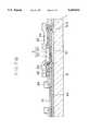
- FIG. 4is a fragmentary enlarged view of the active-matrix substrate in a portion around a thin film resistor thereof;
- FIGS. 5 (a) and 5(b)are sectional views taken along line A--A and line B--B, respectively, of FIG. 4;
- FIG. 6is a sectional view of a pixel portion of the active-matrix substrate shown in FIG. 1;
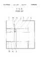
- FIGS. 7(a) and 7(b)are an explanatory plan view and an explanatory sectional view, respectively, of an embodiment of an active-matrix substrate having a thin film resistor comprising an amorphous silicon layer and its silicide layer;
- FIG. 8is a schematic equivalent circuit diagram of a conventional active-matrix substrate.
- a matrix-type display devicesuch as an LCD includes a pair of transparent insulative substrates such as made of glass or a plastic, and a display material such as a liquid crystal sandwiched between the substrates. Each substrate has components, such as electrodes, for selectively applying a voltage to the display material.
- one transparent insulative substrateis provided with switching elements such as TFTs for turning ON or OFF desired pixels for displaying a desired image.
- FIG. 1shows, on an equivalent circuit basis, the pattern of an active-matrix substrate comprising such a transparent insulative substrate having TFTs and pixel electrodes.
- drain electrode 16 of a TFT 1is connected to a pixel electrode 2 which is connected to a capacitor 3.
- Gate electrode 14 of the TFT 1is connected to a gate signal line 4 while source electrode 15 thereof is connected to a source signal line 5.
- the signal lines 4 and 5terminate in input terminals 4a and 5a, respectively, at one ends thereof for receiving signals from an external drive circuit.
- the present inventionis characterized in that each of the input terminals 4a and 5a is connected to a shortcircuiting ring 7 through a thin film resistor 6 of 10 to 500 k ⁇ .
- the thin film resistor 7 of 10 k ⁇ to 500 k ⁇ provided intermediate between each of the input terminals 4a,5a and the shortcircuiting ring 7can be formed simultaneously with the formation of the TFT 1 or capacitor 3 in the same process without requiring a special fabrication process therefor, while being capable of serving as a shortcircuiting line for discharging static electricity in such a short time as not to cause troubles such as shifting of the threshold voltage of TFT and as an insulator when the substrate is tested for its characteristics of pixels such as TFT or capacitor.
- the resistance of the thin film resistoris preferably as low as possible.
- the repeated intensive studyhas led to the finding that if there is provided a shortcircuiting circuit enabling the voltage of generated static electricity to decrease to 50 V or below in 0.01 seconds, the threshold voltage of TFT will not shift and hence the troubles due to threshold shift will not occur and, in addition thereto, there is no fear of a break down of a signal line or a breakdown of a insulator film intermediate between signal lines due to discharge of static electricity.
- the R-C constanthas to be 0.001 seconds or less.
- the thin film resistoris required to have a resistance of about 500 k ⁇ or lower. This resistance is desirably as low as possible to make static electricity to escape, preferably 300 k ⁇ or lower, more preferably 100 k ⁇ or lower.
- FIG. 2illustrates the relation among a testing circuit, equivalent circuit of one pixel and a shortcircuiting ring.
- the section defined by the broken line Pdepicts one pixel on the substrate shown in FIG. 1.
- the circuit shownincludes a TFT 1, a capacitor 3, a gate signal line 4, a source signal line 5, and a thin film resistor 6 (represented by R 3 ) connected between an input terminal 5a and a shortcircuiting ring 7.
- the testing circuitincludes a resistor R 2 and an operational amplifier OP which are connected to the source signal line 5 for serving as, for example, an integrator. Between the input and output of the operational amplifier is connected a capacitor C. A signal is input to an input terminal IP of the source signal line 5 through a resistor R 1 . In this configuration, electric charge I cs accumulated in the pixel section is detected from the output OUT of the testing circuit 9. The current output from this testing circuit 9 is current I M shunted from the current I cs of the electric charge accumulated within the pixel to the testing circuit side.
- the resistor R 2 of the testing circuit 9usually has a resistance of 1 k ⁇ or lower and, hence, the higher the resistance of the resistor R 3 comprising the thin film resistor 6, the lesser the leakage current grows and the more accurate test can be expected.
- the resistance of the resistor R 3is preferably 10 k ⁇ or higher, more preferably 50 k ⁇ or higher.
- the thin film resistor 6 with its resistancethus set allows the electric charge of the pixel to be accurately measured, thereby achieving the test on the substrate for its characteristics of pixel such as TFT or capacitor characteristics or for a possible shortcircuit between signal lines.
- FIG. 4is an enlarged plan view of the thin film resistor and its periphery shown in FIG. 1;
- FIGS. 5(a) and 5(b)are sectional views taken along lines A--A and B--B, respectively, of FIG. 4;
- FIG. 6is a sectional view of a pixel portion.
- This exampleis directed to an active-matrix substrate having a thin film resistor 6 comprising a transparent conductive film, such as an ITO film, which is also used for the electrode of a capacitor.
- a transparent conductive filmsuch as an ITO film
- the thin film resistor 6 hereinis formed in a zigzag configuration as shown in FIG. 4.
- the configuration of the the thin film resistor 6is not limited thereto since the resistance thereof depends on the thickness, width and length thereof.
- the ITO filmis suitably 0.05 to 0.2 ⁇ m thick for facilitating the patterning thereof and for avoiding a cut-off of the pattern thereof and a shortcircuit due to unevenness.
- the ITO filmdesirably has a sheet resistance of 100 to 400 ⁇ per unit area.
- the transparent conductive film such as ITO filmis an oxide film
- the resistivity thereofcan be adjusted by adjusting the flow rate of oxygen in forming the oxide film.
- FIG. 3shows the relation between the flow rate of oxygen and the sheet resistance of oxide film having a thickness in the aforementioned range.
- the sheet resistance per unit area of oxide film having a thickness of about 0.05 to about 0.2 ⁇ mis adjusted to 100 to 400 ⁇ by setting the flow rate of oxygen to about 6 to about 10 sccm.
- the flow rate of oxygenis set to about 1 to about 3 sccm to adjust the sheet resistance of the ITO film to about 20 to about 30 ⁇ .
- the active-matrix substrate according to this exampleis fabricated by the following method. Referring to FIG. 6, on a transparent insulative film 8 such as made of glass is formed a transparent conductive film of ITO, tin oxide, indium oxide or the like having a thickness of 0.05 to 0.2 ⁇ m to form a capacitor electrode 31. At this time the thin film resistor 6 is simultaneously formed as interconnecting the shortcircuiting ring 7 and the input terminal 5a of source signal line 5 or input terminal 4a of gate signal line 4.
- the thin film resistor 6is so formed as to have the same thickness as the capacitor electrode 31, i.e., 0.05 to 0.2 ⁇ m, a width of 5 to 20 ⁇ m, a length of 1 to 3 mm in total, and a sheet resistance of about 100 to about 400 ⁇ , thereby making the thin film resistor 6 have a resistance of about 10 to about 500 k ⁇ which allows a TFT or insulator film to be prevented from being broken and the substrate in a state before being assembled into a display device to be tested for its pixel characteristics.
- the resistivity of the thin film resistorcan readily be adjusted by adjusting the flow rate of oxygen used in sputtering, for example, an ITO film.
- a capacitor insulating film 32is formed by CVD, sputtering, EB evaporation or a like process, followed by forming a contact hole 33 extending to the capacitor electrode 31 to provide connection between the capacitor electrode 31 and the gate signal line 4.
- contact holes 34 and 35are also formed at terminal portions of the thin film resistor 6 to connect the thin film resistor 6 to the shortcircuiting ring 7 and to the source or gate terminal 5a or 4a, as shown in FIGS. 5 and 5b.
- a metal film of Cr, Ta, Mo or the likeis formed by sputtering, vacuum vapor deposition, CVD or a like process to form gate signal line 4 and gate electrode 14.
- the shortcircuiting ring 7 and the input terminal 5a of the source signal line 5 or the input terminal 4a of the gate signal line 4are formed as connecting to the thin film resistor 6, as shown in FIG. 4.
- the pixel electrode 2 shown in FIG. 1is formed from a transparent electrode material such as ITO.
- ITO film 2a of the pixel electrode materialis retained in a region of the input terminal 4a (5a) to faciliate the connection to an external circuit. Further, as shown in FIG.
- an Si 3 N 4 filmto serve as a gate insulating film 11, a non-doped amorphous silicon layer 12 and an etch stopper 17 such as of Si 3 N 4 by plasma CVD or a like process, followed by patterning the etch stopper 17.
- phosphorus-doped amorphous silicon layer 13to serve as a contact layer is formed, followed by forming a contact hole 11c for providing connection between the pixel electrode 2 and the drain electrode 16 by a patterning process.
- films of, for example, Cr and Alare formed by sputtering or the like, then patterned to form the source signal line 5 with source electrode 15 and the drain electrode 16.
- the source signal lineis multilayered as comprising a lower layer of a high melting point metal such as Cr, Mo, Ta, W or Ni having a thickness of about 0.01 to about 0.2 ⁇ m and an upper layer of a low-resistance metal such as Al, Ag or Cu
- advantageswill result that mutual diffusion between the underlying amorphous silicon layer and the low-resistance metal such as Al can be prevented while low-resistance source interconnection can be realized.
- unnecessary portions of the amorphous silicon layers 12 and 13are removed using the source signal line 5, source electrode 15 and drain electrode 16 as a mask.
- a protective film 18such as of Si 3 N 4 is formed by CVD, sputtering, plasma CVD or a like process.
- the active-matrix substrateis completed.
- the thin film resistorsuch as of ITO film is formed simultaneously with the formation of the capacitor in the present example
- the thin film resistormay be formed simultaneously with the formation of the pixel electrode. In this case, also, it is possible to easily form the thin film resistor without requiring a special process therefor.
- FIGS. 7(a) and (b)illustrate a portion including the thin film resistor in plan and in section, respectively.
- the thin film resistor 6is preferably formed in the TFT fabrication process, as in Example 1.
- the etch stopper and non-doped amorphous silicon layer 62are successively patterned in an island configuration and then unnecessary portions of the amorphous silicon layer are removed, followed by patterning the etch stopper in the channel region of TFT and in the region for the thin film resistor 6. At this time, the insulating film in the region for the thin film resistor which has been formed simultaneously with the etch stopper is removed.
- the amorphous silicon layeris doped with phosphorus by ion doping technique to turn it into a phosphorus-doped amorphous silicon layer.
- the doping of phosphorusprovides ohmic contact in the TFT section. Therefore, it is unnecessary to dope the amorphous silicon layer only for the purpose of forming a silicide film in the region for the thin film resistor 6.
- the use of the ion doping techniqueoffers an advantage over a method of independently forming phosphorus-doped amorphous silicon layers that the step of protecting the silicide resistor can be omitted since there is no need to provide the step of removing the phosphorus-doped amorphous silicon layer after the formation of the electrodes of source and drain.
- a pixel electrodeis then formed, followed by the formation of contact holes 61a and 61b. If a transparent conductive film 41 formed in the formation of the pixel electrode or capacitor electrode is retained on the input terminal 4a, the input terminal will be advantageously connected to a lead terminal of an external circuit.
- the oxide film and the like on the amorphous silicon layer 62are removed using buffered hydrofluoric acid (BHF) or the like, and thereafter Cr film 64 and Al film 65 are formed by sputtering or the like at a substrate temperature of 200° to 300° C. and then patterned to form source signal line and drain electrode.
- BHFbuffered hydrofluoric acid
- Cr film 64 and Al film 65are formed by sputtering or the like at a substrate temperature of 200° to 300° C. and then patterned to form source signal line and drain electrode.
- a Cr silicide film 63is formed as having a thickness of several tens angstroms by the reaction of Cr and amorphous silicon.
- the sheet resistance per unit area of the silicide film having such thicknessis about 1 to about 10 k ⁇ .
- the thin film resistor in the configuration shown in FIG. 7readily provides a resistance of 10 to 500 k ⁇ .
- a non-doped amorphous silicon layer of about 0.1 ⁇ m thicknesshas a sheet resistance per unit area of about 10 ⁇ 10 13 to about 10 ⁇ 10 15 ⁇
- a phosphorus-doped amorphous silicon layer of the same thicknesshas a sheet resistance per unit area of about 1 ⁇ 10 6 to about 10 ⁇ 10 8 ⁇ .
- the metal filmis formed on the amorphous silicon layer as having a double layer structure comprising Cr layer and Al layer.
- the high melting point metal having a relatively high resistancesuch as Cr, Mo, Ta, W or Ni is preferable to form the silicide while in contrast the source signal line to be formed simultaneously with silicide is required to have a low resistance.
- the upper metal layeris formed of a metal of low resistance such as Al, Ag or Cu.
- the semiconductor layeris formed of amorphous silicon in the present example, it may be formed of polysilicon instead.
- Cris used in the formation of the silicide film, the use of Mo, Ta, W, Ni, or the like will provide a silicide film of a sheet resistance substantially equal to that of the silicide film formed using Cr.
- a capacitoris provided in any of the foregoing examples, it is needless to say that the present invention is applicable to the case of a substrate not provided with a capacitor.
- the input terminal of each of source signal line and gate signal lineis connected to a shortcircuiting ring through a thin film resistor having a resistance of 10 to 500 k ⁇ .
- the TFTs of the substratecan be prevented from being broken even when the substrate is charged with static electricity, and signal lines and interlayer insulator films therebetween can be protected from being broken by discharge of static electricity between signal lines.
- the active-matrix substrate of the present inventioncan be tested in a state prior to being assembled into a display device for its pixel characteristics such as TFT characteristics and for possible abnormalities such as a shortcircuit between signal lines, it is possible to immediately feed back the cause of an abnormality to the associated fabrication process so as to refine the process, and further, to eliminate a defective substrate before bonded to a counterpart substrate. Accordingly, there is no likelihood of wasting expensive parts of the couterpart substrate such as a color filter, thus leading to a great contribution to an improved production yield and less costly production.
Landscapes
- Physics & Mathematics (AREA)
- Nonlinear Science (AREA)
- Engineering & Computer Science (AREA)
- Microelectronics & Electronic Packaging (AREA)
- Mathematical Physics (AREA)
- Chemical & Material Sciences (AREA)
- Crystallography & Structural Chemistry (AREA)
- General Physics & Mathematics (AREA)
- Optics & Photonics (AREA)
- Liquid Crystal (AREA)
Abstract
Description
Claims (4)
Applications Claiming Priority (2)
| Application Number | Priority Date | Filing Date | Title |
|---|---|---|---|
| JP6-153621 | 1994-07-05 | ||
| JP15362194AJPH0822024A (en) | 1994-07-05 | 1994-07-05 | Active matrix substrate and manufacturing method thereof |
Publications (1)
| Publication Number | Publication Date |
|---|---|
| US5650834Atrue US5650834A (en) | 1997-07-22 |
Family
ID=15566498
Family Applications (1)
| Application Number | Title | Priority Date | Filing Date |
|---|---|---|---|
| US08/363,030Expired - Fee RelatedUS5650834A (en) | 1994-07-05 | 1994-12-23 | Active-matrix device having silicide thin film resistor disposed between an input terminal and a short-circuit ring |
Country Status (2)
| Country | Link |
|---|---|
| US (1) | US5650834A (en) |
| JP (1) | JPH0822024A (en) |
Cited By (101)
| Publication number | Priority date | Publication date | Assignee | Title |
|---|---|---|---|---|
| US5771083A (en)* | 1995-10-16 | 1998-06-23 | Sharp Kabushiki Kaisha | Active matrix substrate and liquid crystal display device |
| US5793460A (en)* | 1995-08-22 | 1998-08-11 | Lg Electronics Inc. | Liquid crystal display device and method for manufacturing the same |
| US5828428A (en)* | 1995-01-27 | 1998-10-27 | Samsung Electronics Co., Ltd. | Resistive circuit for a thin film transistor liquid crystal display and a method for manufacturing the same |
| US5838051A (en)* | 1995-04-27 | 1998-11-17 | Vanguard International Semiconductor Corporation | Tungsten policide contacts for semiconductor devices |
| US6005647A (en)* | 1996-07-22 | 1999-12-21 | Lg Electronics Inc. | Shorting bars for a liquid crystal display and method of forming the same |
| EP0993038A1 (en)* | 1998-08-31 | 2000-04-12 | Canon Kabushiki Kaisha | TFT matrix panel |
| US6052104A (en)* | 1995-07-12 | 2000-04-18 | Lg Electronics Inc. | Structure and operation method of LCD |
| US6072550A (en)* | 1996-06-11 | 2000-06-06 | Samsung Electronics Co., Ltd. | Liquid crystal display having resistive electrostatic discharge protection devices with resistance no greater than 1 MOHM and method of fabrication |
| US6106907A (en)* | 1996-06-25 | 2000-08-22 | Canon Kabushiki Kaisha | Electrode plate, liquid crystal device and production thereof |
| US6229140B1 (en) | 1995-10-27 | 2001-05-08 | Canon Kabushiki Kaisha | Displacement information detection apparatus |
| US6232944B1 (en)* | 1996-04-05 | 2001-05-15 | Matsushita Electric Industrial Co., Ltd. | Driving method, drive IC and drive circuit for liquid crystal display |
| US6323051B1 (en)* | 1999-03-10 | 2001-11-27 | Sharp Kabushiki Kaisha | Method of manufacturing liquid crystal display |
| US20020126250A1 (en)* | 1998-02-19 | 2002-09-12 | Seiko Epson Corporation | Active-matrix substrate, electro-optical device, method for manufacturing active-matrix substrate, and electronic equipment |
| US6613650B1 (en)* | 1995-07-31 | 2003-09-02 | Hyundai Electronics America | Active matrix ESD protection and testing scheme |
| US20040027502A1 (en)* | 1999-08-31 | 2004-02-12 | Fujitsu Display Technologies Corporation | Liquid crystal display |
| US20040041958A1 (en)* | 2002-09-03 | 2004-03-04 | Yong-Sup Hwang | Array substrate for LCD device having double-layered gate and data lines and manufacturing method thereof |
| US20040201056A1 (en)* | 2003-04-14 | 2004-10-14 | Semiconductor Energy Laboratory Co., Ltd. | Audio signal processing circuit and a display device incorporating the same |
| US20040263706A1 (en)* | 2003-06-30 | 2004-12-30 | Lg.Philips Lcd Co., Ltd. | Array substrate for LCD device having double-layered metal structure and manufacturing method thereof |
| US20050052384A1 (en)* | 2003-07-29 | 2005-03-10 | Seiko Epson Corporation | Driving circuit, method for protecting the same, electro-optical apparatus, and electronic apparatus |
| US20050078348A1 (en)* | 2003-09-30 | 2005-04-14 | Wen-Jian Lin | Structure of a micro electro mechanical system and the manufacturing method thereof |
| US20050128112A1 (en)* | 2003-12-11 | 2005-06-16 | Semiconductor Energy Laboratory Co., Ltd. | D/A converter for a digital signal after non-linear A/D conversion, audio signal processing circuit and liquid crystal display device including the same |
| US20050211984A1 (en)* | 2004-03-25 | 2005-09-29 | Semiconductor Energy Laboratory Co., Ltd. | Light emitting device, method for manufacturing thereof and electronic appliance |
| WO2005078693A3 (en)* | 2004-02-03 | 2005-10-13 | Idc Llc | Driver voltage adjuster |
| US20060077519A1 (en)* | 2004-09-27 | 2006-04-13 | Floyd Philip D | System and method for providing thermal compensation for an interferometric modulator display |
| US20060181500A1 (en)* | 2005-02-17 | 2006-08-17 | Seiko Epson Corporation | Electro-optical device, method of manufacturing electro-optical device, and electronic apparatus |
| US20060214008A1 (en)* | 2005-03-28 | 2006-09-28 | Semiconductor Energy Laboratory Co., Ltd. | Memory device and manufacturing method the same |
| US20060257070A1 (en)* | 2003-05-26 | 2006-11-16 | Wen-Jian Lin | Optical interference display cell and method of making the same |
| US20060256420A1 (en)* | 2003-06-24 | 2006-11-16 | Miles Mark W | Film stack for manufacturing micro-electromechanical systems (MEMS) devices |
| US20060279685A1 (en)* | 1996-01-26 | 2006-12-14 | Semiconductor Energy Laboratory Co., Ltd. | Liquid crystal electro-optical device |
| US20060279495A1 (en)* | 2005-05-05 | 2006-12-14 | Moe Douglas P | Dynamic driver IC and display panel configuration |
| KR100656900B1 (en)* | 1999-12-13 | 2006-12-15 | 삼성전자주식회사 | Thin film transistor substrate for liquid crystal display device having electrostatic discharge structure and manufacturing method thereof |
| US20070155051A1 (en)* | 2005-12-29 | 2007-07-05 | Chun-Ming Wang | Method of creating MEMS device cavities by a non-etching process |
| US7250315B2 (en) | 2002-02-12 | 2007-07-31 | Idc, Llc | Method for fabricating a structure for a microelectromechanical system (MEMS) device |
| US7256922B2 (en) | 2004-07-02 | 2007-08-14 | Idc, Llc | Interferometric modulators with thin film transistors |
| US20070228156A1 (en)* | 2006-03-28 | 2007-10-04 | Household Corporation | Interoperability facilitator |
| US20070236774A1 (en)* | 2006-04-10 | 2007-10-11 | Evgeni Gousev | Interferometric optical display system with broadband characteristics |
| US20070247401A1 (en)* | 2006-04-19 | 2007-10-25 | Teruo Sasagawa | Microelectromechanical device and method utilizing nanoparticles |
| US20070247696A1 (en)* | 2006-04-19 | 2007-10-25 | Teruo Sasagawa | Microelectromechanical device and method utilizing a porous surface |
| US7297471B1 (en) | 2003-04-15 | 2007-11-20 | Idc, Llc | Method for manufacturing an array of interferometric modulators |
| US20070279730A1 (en)* | 2006-06-01 | 2007-12-06 | David Heald | Process and structure for fabrication of mems device having isolated egde posts |
| US20080062373A1 (en)* | 2006-09-11 | 2008-03-13 | Samsung Sdi Co., Ltd. | Flat panel display device |
| US7349136B2 (en) | 2004-09-27 | 2008-03-25 | Idc, Llc | Method and device for a display having transparent components integrated therein |
| US7369296B2 (en) | 2004-09-27 | 2008-05-06 | Idc, Llc | Device and method for modifying actuation voltage thresholds of a deformable membrane in an interferometric modulator |
| US7369292B2 (en) | 2006-05-03 | 2008-05-06 | Qualcomm Mems Technologies, Inc. | Electrode and interconnect materials for MEMS devices |
| US7373026B2 (en) | 2004-09-27 | 2008-05-13 | Idc, Llc | MEMS device fabricated on a pre-patterned substrate |
| US7382515B2 (en) | 2006-01-18 | 2008-06-03 | Qualcomm Mems Technologies, Inc. | Silicon-rich silicon nitrides as etch stops in MEMS manufacture |
| US20080158647A1 (en)* | 2004-09-27 | 2008-07-03 | Idc, Llc | Interferometric modulator array with integrated mems electrical switches |
| US20080158648A1 (en)* | 2006-12-29 | 2008-07-03 | Cummings William J | Peripheral switches for MEMS display test |
| US20080160251A1 (en)* | 2006-12-29 | 2008-07-03 | Cummings William J | Switches for shorting during MEMS etch release |
| US7405861B2 (en) | 2004-09-27 | 2008-07-29 | Idc, Llc | Method and device for protecting interferometric modulators from electrostatic discharge |
| US7405863B2 (en) | 2006-06-01 | 2008-07-29 | Qualcomm Mems Technologies, Inc. | Patterning of mechanical layer in MEMS to reduce stresses at supports |
| US20080192029A1 (en)* | 2007-02-08 | 2008-08-14 | Michael Hugh Anderson | Passive circuits for de-multiplexing display inputs |
| US7417783B2 (en) | 2004-09-27 | 2008-08-26 | Idc, Llc | Mirror and mirror layer for optical modulator and method |
| US7420728B2 (en) | 2004-09-27 | 2008-09-02 | Idc, Llc | Methods of fabricating interferometric modulators by selectively removing a material |
| US7450295B2 (en) | 2006-03-02 | 2008-11-11 | Qualcomm Mems Technologies, Inc. | Methods for producing MEMS with protective coatings using multi-component sacrificial layers |
| US7471444B2 (en) | 1996-12-19 | 2008-12-30 | Idc, Llc | Interferometric modulation of radiation |
| US7485236B2 (en) | 2003-08-26 | 2009-02-03 | Qualcomm Mems Technologies, Inc. | Interference display cell and fabrication method thereof |
| US7492502B2 (en) | 2004-09-27 | 2009-02-17 | Idc, Llc | Method of fabricating a free-standing microstructure |
| US7527996B2 (en) | 2006-04-19 | 2009-05-05 | Qualcomm Mems Technologies, Inc. | Non-planar surface structures and process for microelectromechanical systems |
| US7534640B2 (en) | 2005-07-22 | 2009-05-19 | Qualcomm Mems Technologies, Inc. | Support structure for MEMS device and methods therefor |
| US7547565B2 (en) | 2005-02-04 | 2009-06-16 | Qualcomm Mems Technologies, Inc. | Method of manufacturing optical interference color display |
| US7547568B2 (en) | 2006-02-22 | 2009-06-16 | Qualcomm Mems Technologies, Inc. | Electrical conditioning of MEMS device and insulating layer thereof |
| US7550794B2 (en) | 2002-09-20 | 2009-06-23 | Idc, Llc | Micromechanical systems device comprising a displaceable electrode and a charge-trapping layer |
| US7553684B2 (en) | 2004-09-27 | 2009-06-30 | Idc, Llc | Method of fabricating interferometric devices using lift-off processing techniques |
| US7566664B2 (en) | 2006-08-02 | 2009-07-28 | Qualcomm Mems Technologies, Inc. | Selective etching of MEMS using gaseous halides and reactive co-etchants |
| US20090237040A1 (en)* | 2008-03-18 | 2009-09-24 | Qualcomm Mems Technologies, Inc. | family of current/power-efficient high voltage linear regulator circuit architectures |
| US7623287B2 (en) | 2006-04-19 | 2009-11-24 | Qualcomm Mems Technologies, Inc. | Non-planar surface structures and process for microelectromechanical systems |
| US7630114B2 (en) | 2005-10-28 | 2009-12-08 | Idc, Llc | Diffusion barrier layer for MEMS devices |
| US20100014146A1 (en)* | 2008-07-17 | 2010-01-21 | Qualcomm Mems Technologies, Inc. | Encapsulation methods for interferometric modulator and mems devices |
| US7667884B2 (en) | 2004-09-27 | 2010-02-23 | Qualcomm Mems Technologies, Inc. | Interferometric modulators having charge persistence |
| US7684104B2 (en) | 2004-09-27 | 2010-03-23 | Idc, Llc | MEMS using filler material and method |
| US7702192B2 (en) | 2006-06-21 | 2010-04-20 | Qualcomm Mems Technologies, Inc. | Systems and methods for driving MEMS display |
| US7763546B2 (en) | 2006-08-02 | 2010-07-27 | Qualcomm Mems Technologies, Inc. | Methods for reducing surface charges during the manufacture of microelectromechanical systems devices |
| US20100202038A1 (en)* | 2006-12-20 | 2010-08-12 | Qualcomm Mems Technologies, Inc. | Mems device and interconnects for same |
| US7777715B2 (en) | 2006-06-29 | 2010-08-17 | Qualcomm Mems Technologies, Inc. | Passive circuits for de-multiplexing display inputs |
| US7781850B2 (en) | 2002-09-20 | 2010-08-24 | Qualcomm Mems Technologies, Inc. | Controlling electromechanical behavior of structures within a microelectromechanical systems device |
| US20100265563A1 (en)* | 2005-08-19 | 2010-10-21 | Qualcomm Mems Technologies, Inc. | Electromechanical device configured to minimize stress-related deformation and methods for fabricating same |
| US7843410B2 (en) | 2004-09-27 | 2010-11-30 | Qualcomm Mems Technologies, Inc. | Method and device for electrically programmable display |
| US7884788B2 (en) | 2003-08-04 | 2011-02-08 | Semiconductor Energy Laboratory Co., Ltd | Liquid crystal display device and electronic apparatus |
| US7889163B2 (en) | 2004-08-27 | 2011-02-15 | Qualcomm Mems Technologies, Inc. | Drive method for MEMS devices |
| US20110114956A1 (en)* | 2009-11-13 | 2011-05-19 | Sun Park | Organic Light Emitting Display Apparatus and Method of Manufacturing the Same |
| US20110185322A1 (en)* | 2010-01-25 | 2011-07-28 | Palo Alto Research Center Incorporated | Method of in-process intralayer yield detection, interlayer shunt detection and correction |
| US20120012854A1 (en)* | 2009-04-10 | 2012-01-19 | Toshihiro Kaneko | Active matrix substrate, display panel, display device, and laser irradiation method |
| CN101847648B (en)* | 2009-03-23 | 2012-11-21 | 北京京东方光电科技有限公司 | Active matrix organic light-emitting diode pixel structure and manufacturing method thereof |
| US8736590B2 (en) | 2009-03-27 | 2014-05-27 | Qualcomm Mems Technologies, Inc. | Low voltage driver scheme for interferometric modulators |
| US8791897B2 (en) | 2004-09-27 | 2014-07-29 | Qualcomm Mems Technologies, Inc. | Method and system for writing data to MEMS display elements |
| US20140233170A1 (en)* | 2007-06-21 | 2014-08-21 | Apple Inc. | Handheld Electronic Device With Cable Grounding |
| US8830557B2 (en) | 2007-05-11 | 2014-09-09 | Qualcomm Mems Technologies, Inc. | Methods of fabricating MEMS with spacers between plates and devices formed by same |
| US8928967B2 (en) | 1998-04-08 | 2015-01-06 | Qualcomm Mems Technologies, Inc. | Method and device for modulating light |
| US8971675B2 (en) | 2006-01-13 | 2015-03-03 | Qualcomm Mems Technologies, Inc. | Interconnect structure for MEMS device |
| US9110289B2 (en) | 1998-04-08 | 2015-08-18 | Qualcomm Mems Technologies, Inc. | Device for modulating light with multiple electrodes |
| US20160013264A1 (en)* | 2013-03-06 | 2016-01-14 | Seiko Epson Corporation | Electro-optical device, electronic apparatus, and drive circuit |
| US20160064413A1 (en)* | 2014-09-02 | 2016-03-03 | Boe Technology Group Co., Ltd. | Array substrate, method for manufacturing the same and display device |
| CN107407845A (en)* | 2015-03-18 | 2017-11-28 | 凸版印刷株式会社 | Thin film transistor array, image display device and manufacturing method of thin film transistor array |
| US9838059B2 (en) | 2007-06-21 | 2017-12-05 | Apple Inc. | Handheld electronic touch screen communication device |
| CN109991769A (en)* | 2017-12-27 | 2019-07-09 | 夏普株式会社 | Display device, manufacturing method of display device, and inspection method of display device |
| US20190221277A1 (en)* | 2018-01-17 | 2019-07-18 | International Business Machines Corporation | One-time-programmable memory in a high-density three-dimensional structure |
| US10594351B2 (en) | 2008-04-11 | 2020-03-17 | Apple Inc. | Portable electronic device with two-piece housing |
| US10782153B2 (en) | 2016-03-08 | 2020-09-22 | Analog Devices Global | Multiturn sensor arrangement and readout |
| US11460521B2 (en) | 2019-03-18 | 2022-10-04 | Analog Devices International Unlimited Company | Multiturn sensor arrangement |
| US20220344224A1 (en)* | 2020-02-27 | 2022-10-27 | Hefei Boe Joint Technology Co., Ltd. | Motherboard and manufacturing method for motherboard |
Families Citing this family (6)
| Publication number | Priority date | Publication date | Assignee | Title |
|---|---|---|---|---|
| TW538266B (en)* | 1999-04-02 | 2003-06-21 | Matsushita Electric Industrial Co Ltd | Active matrix array substrate and its manufacturing method |
| JP4202571B2 (en)* | 1999-12-21 | 2008-12-24 | 東芝松下ディスプレイテクノロジー株式会社 | Liquid crystal display device and manufacturing method thereof |
| JP2003043508A (en)* | 2001-07-27 | 2003-02-13 | Hitachi Ltd | Liquid crystal display |
| JPWO2004068445A1 (en) | 2003-01-30 | 2006-05-25 | 東芝松下ディスプレイテクノロジー株式会社 | Display, wiring board and manufacturing method thereof |
| KR101845480B1 (en)* | 2010-06-25 | 2018-04-04 | 가부시키가이샤 한도오따이 에네루기 켄큐쇼 | Method for manufacturing semiconductor device |
| CN109801909B (en)* | 2018-06-12 | 2024-08-20 | 京东方科技集团股份有限公司 | Array substrate mother board and manufacturing method thereof, array substrate and display device |
Citations (18)
| Publication number | Priority date | Publication date | Assignee | Title |
|---|---|---|---|---|
| JPS62219662A (en)* | 1986-03-20 | 1987-09-26 | Fujitsu Ltd | Amorphous silicon thin film transistor matrix array |
| JPS643827A (en)* | 1987-06-25 | 1989-01-09 | Mitsubishi Electric Corp | Optical disk device |
| US4857907A (en)* | 1986-04-30 | 1989-08-15 | 501 Sharp Kabushiki Kaisha | Liquid-crystal display device |
| JPH02186326A (en)* | 1989-01-13 | 1990-07-20 | Sharp Corp | Active matrix substrate |
| JPH03116117A (en)* | 1989-09-29 | 1991-05-17 | Toshiba Corp | Drive circuit board for display devices |
| US5068748A (en)* | 1989-10-20 | 1991-11-26 | Hosiden Corporation | Active matrix liquid crystal display device having improved electrostatic discharge protection |
| US5200876A (en)* | 1989-04-10 | 1993-04-06 | Matsushita Electric Industrial Co., Ltd. | Electrostatic breakdown protection circuit |
| JPH05181157A (en)* | 1991-12-27 | 1993-07-23 | Sharp Corp | Thin film transistor substrate |
| US5233448A (en)* | 1992-05-04 | 1993-08-03 | Industrial Technology Research Institute | Method of manufacturing a liquid crystal display panel including photoconductive electrostatic protection |
| US5283449A (en)* | 1990-08-09 | 1994-02-01 | Nec Corporation | Semiconductor integrated circuit device including two types of MOSFETS having source/drain region different in sheet resistance from each other |
| US5323254A (en)* | 1992-04-03 | 1994-06-21 | U.S. Philips Corporation | Display device with electrostatic discharge protection |
| US5335102A (en)* | 1990-05-11 | 1994-08-02 | Sharp Kabushiki Kaisha | Liquid crystal display element and method for treating defective pixels therein |
| JPH06258668A (en)* | 1993-03-05 | 1994-09-16 | Toshiba Corp | Matrix array substrate, manufacturing method thereof, and liquid crystal display device using the same |
| US5373337A (en)* | 1993-12-09 | 1994-12-13 | Eastman Kodak Company | Method and apparatus for sorting excessive core set film |
| US5467882A (en)* | 1992-11-07 | 1995-11-21 | Goldstar Co., Ltd. | Signal line structure for a TFT-LCD and method for fabricating the same |
| US5471329A (en)* | 1992-12-21 | 1995-11-28 | Sharp Kabushiki Kaisha | Active matrix type liquid crystal display panel and a method for producing the same, having a construction capable of preventing breakdown of the switching elements or deterioration due to static electricity |
| US5498573A (en)* | 1989-11-29 | 1996-03-12 | General Electric Company | Method of making multi-layer address lines for amorphous silicon liquid crystal display devices |
| US5504348A (en)* | 1992-08-13 | 1996-04-02 | Casio Computer Co., Ltd. | Thin-film transistor array and liquid crystal display device using the thin-film transistor array |
- 1994
- 1994-07-05JPJP15362194Apatent/JPH0822024A/enactivePending
- 1994-12-23USUS08/363,030patent/US5650834A/ennot_activeExpired - Fee Related
Patent Citations (18)
| Publication number | Priority date | Publication date | Assignee | Title |
|---|---|---|---|---|
| JPS62219662A (en)* | 1986-03-20 | 1987-09-26 | Fujitsu Ltd | Amorphous silicon thin film transistor matrix array |
| US4857907A (en)* | 1986-04-30 | 1989-08-15 | 501 Sharp Kabushiki Kaisha | Liquid-crystal display device |
| JPS643827A (en)* | 1987-06-25 | 1989-01-09 | Mitsubishi Electric Corp | Optical disk device |
| JPH02186326A (en)* | 1989-01-13 | 1990-07-20 | Sharp Corp | Active matrix substrate |
| US5200876A (en)* | 1989-04-10 | 1993-04-06 | Matsushita Electric Industrial Co., Ltd. | Electrostatic breakdown protection circuit |
| JPH03116117A (en)* | 1989-09-29 | 1991-05-17 | Toshiba Corp | Drive circuit board for display devices |
| US5068748A (en)* | 1989-10-20 | 1991-11-26 | Hosiden Corporation | Active matrix liquid crystal display device having improved electrostatic discharge protection |
| US5498573A (en)* | 1989-11-29 | 1996-03-12 | General Electric Company | Method of making multi-layer address lines for amorphous silicon liquid crystal display devices |
| US5335102A (en)* | 1990-05-11 | 1994-08-02 | Sharp Kabushiki Kaisha | Liquid crystal display element and method for treating defective pixels therein |
| US5283449A (en)* | 1990-08-09 | 1994-02-01 | Nec Corporation | Semiconductor integrated circuit device including two types of MOSFETS having source/drain region different in sheet resistance from each other |
| JPH05181157A (en)* | 1991-12-27 | 1993-07-23 | Sharp Corp | Thin film transistor substrate |
| US5323254A (en)* | 1992-04-03 | 1994-06-21 | U.S. Philips Corporation | Display device with electrostatic discharge protection |
| US5233448A (en)* | 1992-05-04 | 1993-08-03 | Industrial Technology Research Institute | Method of manufacturing a liquid crystal display panel including photoconductive electrostatic protection |
| US5504348A (en)* | 1992-08-13 | 1996-04-02 | Casio Computer Co., Ltd. | Thin-film transistor array and liquid crystal display device using the thin-film transistor array |
| US5467882A (en)* | 1992-11-07 | 1995-11-21 | Goldstar Co., Ltd. | Signal line structure for a TFT-LCD and method for fabricating the same |
| US5471329A (en)* | 1992-12-21 | 1995-11-28 | Sharp Kabushiki Kaisha | Active matrix type liquid crystal display panel and a method for producing the same, having a construction capable of preventing breakdown of the switching elements or deterioration due to static electricity |
| JPH06258668A (en)* | 1993-03-05 | 1994-09-16 | Toshiba Corp | Matrix array substrate, manufacturing method thereof, and liquid crystal display device using the same |
| US5373337A (en)* | 1993-12-09 | 1994-12-13 | Eastman Kodak Company | Method and apparatus for sorting excessive core set film |
Non-Patent Citations (2)
| Title |
|---|
| Murarka, "Properties & Applications Of Silicides", Rensselaer Polytechnic Institute Center for Intergrated Electronics, pp. 275-323. |
| Murarka, Properties & Applications Of Silicides , Rensselaer Polytechnic Institute Center for Intergrated Electronics, pp. 275 323.* |
Cited By (184)
| Publication number | Priority date | Publication date | Assignee | Title |
|---|---|---|---|---|
| US5828428A (en)* | 1995-01-27 | 1998-10-27 | Samsung Electronics Co., Ltd. | Resistive circuit for a thin film transistor liquid crystal display and a method for manufacturing the same |
| US5838051A (en)* | 1995-04-27 | 1998-11-17 | Vanguard International Semiconductor Corporation | Tungsten policide contacts for semiconductor devices |
| US6052104A (en)* | 1995-07-12 | 2000-04-18 | Lg Electronics Inc. | Structure and operation method of LCD |
| US6613650B1 (en)* | 1995-07-31 | 2003-09-02 | Hyundai Electronics America | Active matrix ESD protection and testing scheme |
| US5793460A (en)* | 1995-08-22 | 1998-08-11 | Lg Electronics Inc. | Liquid crystal display device and method for manufacturing the same |
| US5771083A (en)* | 1995-10-16 | 1998-06-23 | Sharp Kabushiki Kaisha | Active matrix substrate and liquid crystal display device |
| US6229140B1 (en) | 1995-10-27 | 2001-05-08 | Canon Kabushiki Kaisha | Displacement information detection apparatus |
| US6617572B2 (en) | 1995-10-27 | 2003-09-09 | Canon Kabushiki Kaisha | Displacement information detection apparatus |
| US20110025938A1 (en)* | 1996-01-26 | 2011-02-03 | Semiconductor Energy Laboratory Co., Ltd. | Liquid crystal electro-optical device |
| US8514361B2 (en)* | 1996-01-26 | 2013-08-20 | Semiconductor Energy Laboratory Co., Ltd. | Liquid crystal having common electrode |
| US20060279685A1 (en)* | 1996-01-26 | 2006-12-14 | Semiconductor Energy Laboratory Co., Ltd. | Liquid crystal electro-optical device |
| US7728942B2 (en)* | 1996-01-26 | 2010-06-01 | Semiconductor Energy Laboratory Co., Ltd. | Liquid crystal electro-optical device |
| US20120287365A1 (en)* | 1996-01-26 | 2012-11-15 | Semiconductor Energy Laboratory Co., Ltd. | Liquid crystal electro-optical device |
| US8199300B2 (en) | 1996-01-26 | 2012-06-12 | Semiconductor Energy Laboratory Co., Ltd. | Liquid crystal device utilizing electric field parallel to substrate |
| US6633272B1 (en)* | 1996-04-05 | 2003-10-14 | Matsushita Electric Industrial Co., Ltd. | Driving method, drive IC and drive circuit for liquid crystal display |
| US6597337B1 (en) | 1996-04-05 | 2003-07-22 | Matsushita Electric Industrial Co., Ltd. | Driving method, drive IC and drive circuit for liquid crystal display |
| US6522318B1 (en) | 1996-04-05 | 2003-02-18 | Matsushita Electric Industrial Co., Ltd. | Driving method, drive IC and drive circuit for liquid crystal display |
| US6232944B1 (en)* | 1996-04-05 | 2001-05-15 | Matsushita Electric Industrial Co., Ltd. | Driving method, drive IC and drive circuit for liquid crystal display |
| US6072550A (en)* | 1996-06-11 | 2000-06-06 | Samsung Electronics Co., Ltd. | Liquid crystal display having resistive electrostatic discharge protection devices with resistance no greater than 1 MOHM and method of fabrication |
| US6500352B1 (en) | 1996-06-19 | 2002-12-31 | Canon Kabushiki Kaisha | Electrode plate, liquid crystal device and production thereof |
| US6106907A (en)* | 1996-06-25 | 2000-08-22 | Canon Kabushiki Kaisha | Electrode plate, liquid crystal device and production thereof |
| US6005647A (en)* | 1996-07-22 | 1999-12-21 | Lg Electronics Inc. | Shorting bars for a liquid crystal display and method of forming the same |
| US7471444B2 (en) | 1996-12-19 | 2008-12-30 | Idc, Llc | Interferometric modulation of radiation |
| US6891523B2 (en) | 1998-02-19 | 2005-05-10 | Seiko Epson Corporation | Active-matrix substrate, electro-optical device, method for manufacturing active-matrix substrate, and electronic equipment |
| US20020126250A1 (en)* | 1998-02-19 | 2002-09-12 | Seiko Epson Corporation | Active-matrix substrate, electro-optical device, method for manufacturing active-matrix substrate, and electronic equipment |
| US8928967B2 (en) | 1998-04-08 | 2015-01-06 | Qualcomm Mems Technologies, Inc. | Method and device for modulating light |
| US9110289B2 (en) | 1998-04-08 | 2015-08-18 | Qualcomm Mems Technologies, Inc. | Device for modulating light with multiple electrodes |
| US7888680B2 (en) | 1998-08-31 | 2011-02-15 | Canon Kabushiki Kaisha | Semiconductor device |
| US7098481B2 (en) | 1998-08-31 | 2006-08-29 | Canon Kabushiki Kaisha | Semiconductor device |
| EP0993038A1 (en)* | 1998-08-31 | 2000-04-12 | Canon Kabushiki Kaisha | TFT matrix panel |
| EP1717853A3 (en)* | 1998-08-31 | 2012-05-30 | Canon Kabushiki Kaisha | TFT matrix panel |
| EP1473768A3 (en)* | 1998-08-31 | 2006-01-11 | Canon Kabushiki Kaisha | TFT matrix panel |
| US20050051779A1 (en)* | 1998-08-31 | 2005-03-10 | Canon Kabushiki Kaisha | Semiconductor device |
| EP1473768A2 (en) | 1998-08-31 | 2004-11-03 | Canon Kabushiki Kaisha | TFT matrix panel |
| US6323051B1 (en)* | 1999-03-10 | 2001-11-27 | Sharp Kabushiki Kaisha | Method of manufacturing liquid crystal display |
| US7342617B2 (en)* | 1999-08-31 | 2008-03-11 | Sharp Kabushiki Kaisha | Liquid crystal display comprising an electrostatic protection element formed between adjacent bus lines |
| US20040027502A1 (en)* | 1999-08-31 | 2004-02-12 | Fujitsu Display Technologies Corporation | Liquid crystal display |
| KR100656900B1 (en)* | 1999-12-13 | 2006-12-15 | 삼성전자주식회사 | Thin film transistor substrate for liquid crystal display device having electrostatic discharge structure and manufacturing method thereof |
| US7642110B2 (en) | 2002-02-12 | 2010-01-05 | Qualcomm Mems Technologies, Inc. | Method for fabricating a structure for a microelectromechanical systems (MEMS) device |
| US7250315B2 (en) | 2002-02-12 | 2007-07-31 | Idc, Llc | Method for fabricating a structure for a microelectromechanical system (MEMS) device |
| US7652740B2 (en)* | 2002-09-03 | 2010-01-26 | Lg Display Co., Ltd. | Array substrate for LCD device having dual metal-layer gate and data lines and manufacturing method thereof |
| US20040041958A1 (en)* | 2002-09-03 | 2004-03-04 | Yong-Sup Hwang | Array substrate for LCD device having double-layered gate and data lines and manufacturing method thereof |
| US7781850B2 (en) | 2002-09-20 | 2010-08-24 | Qualcomm Mems Technologies, Inc. | Controlling electromechanical behavior of structures within a microelectromechanical systems device |
| US7550794B2 (en) | 2002-09-20 | 2009-06-23 | Idc, Llc | Micromechanical systems device comprising a displaceable electrode and a charge-trapping layer |
| US7769190B2 (en)* | 2003-04-14 | 2010-08-03 | Semiconductor Energy Laboratory Co., Ltd. | Audio signal processing circuit and a display device incorporating the same |
| US20040201056A1 (en)* | 2003-04-14 | 2004-10-14 | Semiconductor Energy Laboratory Co., Ltd. | Audio signal processing circuit and a display device incorporating the same |
| US7297471B1 (en) | 2003-04-15 | 2007-11-20 | Idc, Llc | Method for manufacturing an array of interferometric modulators |
| US7706044B2 (en) | 2003-05-26 | 2010-04-27 | Qualcomm Mems Technologies, Inc. | Optical interference display cell and method of making the same |
| US20060257070A1 (en)* | 2003-05-26 | 2006-11-16 | Wen-Jian Lin | Optical interference display cell and method of making the same |
| US20060256420A1 (en)* | 2003-06-24 | 2006-11-16 | Miles Mark W | Film stack for manufacturing micro-electromechanical systems (MEMS) devices |
| US7616369B2 (en) | 2003-06-24 | 2009-11-10 | Idc, Llc | Film stack for manufacturing micro-electromechanical systems (MEMS) devices |
| US7777822B2 (en) | 2003-06-30 | 2010-08-17 | Lg Display Co., Ltd. | Array substrate for LCD device having double-layered metal structure and manufacturing method thereof |
| US20040263706A1 (en)* | 2003-06-30 | 2004-12-30 | Lg.Philips Lcd Co., Ltd. | Array substrate for LCD device having double-layered metal structure and manufacturing method thereof |
| US20110212557A1 (en)* | 2003-06-30 | 2011-09-01 | Won-Ho Cho | Method of manufacturing an array substrate for lcd device having double-layered metal structure |
| US7956949B2 (en) | 2003-06-30 | 2011-06-07 | Lg Display Co., Ltd. | Method of manufacturing an array substrate for LCD device having double-layered metal structure |
| US8432503B2 (en) | 2003-06-30 | 2013-04-30 | Lg Display Co., Ltd. | Method of manufacturing an array substrate for LCD device having doubled-layered metal structure |
| US7605877B2 (en)* | 2003-06-30 | 2009-10-20 | Lg Display Co., Ltd. | Array substrate for LCD device having double-layered metal structure and manufacturing method thereof |
| US20100203687A1 (en)* | 2003-06-30 | 2010-08-12 | Won-Ho Cho | Method of manufacturing an array substrate for lcd device having double-layered metal structure |
| US20080182352A1 (en)* | 2003-06-30 | 2008-07-31 | Won-Ho Cho | Array substrate for LCD device having double-layered metal structure and manufacturing method thereof |
| US20050052384A1 (en)* | 2003-07-29 | 2005-03-10 | Seiko Epson Corporation | Driving circuit, method for protecting the same, electro-optical apparatus, and electronic apparatus |
| US7408535B2 (en) | 2003-07-29 | 2008-08-05 | Seiko Epson Corporation | Driving circuit, method for protecting the same, electro-optical apparatus, and electronic apparatus |
| US7884788B2 (en) | 2003-08-04 | 2011-02-08 | Semiconductor Energy Laboratory Co., Ltd | Liquid crystal display device and electronic apparatus |
| US7485236B2 (en) | 2003-08-26 | 2009-02-03 | Qualcomm Mems Technologies, Inc. | Interference display cell and fabrication method thereof |
| US20050078348A1 (en)* | 2003-09-30 | 2005-04-14 | Wen-Jian Lin | Structure of a micro electro mechanical system and the manufacturing method thereof |
| US7291921B2 (en) | 2003-09-30 | 2007-11-06 | Qualcomm Mems Technologies, Inc. | Structure of a micro electro mechanical system and the manufacturing method thereof |
| US20050128112A1 (en)* | 2003-12-11 | 2005-06-16 | Semiconductor Energy Laboratory Co., Ltd. | D/A converter for a digital signal after non-linear A/D conversion, audio signal processing circuit and liquid crystal display device including the same |
| US7369074B2 (en) | 2003-12-11 | 2008-05-06 | Semiconductor Energy Laboratory Co., Ltd. | D/A converter for a digital signal after non-linear A/D conversion, audio signal processing circuit and liquid crystal display device including the same |
| WO2005078693A3 (en)* | 2004-02-03 | 2005-10-13 | Idc Llc | Driver voltage adjuster |
| US7532194B2 (en) | 2004-02-03 | 2009-05-12 | Idc, Llc | Driver voltage adjuster |
| US20070158657A1 (en)* | 2004-03-25 | 2007-07-12 | Semiconductor Energy Laboratory Co., Ltd. | Light emitting device, method for manufacturing thereof and electronic appliance |
| US20050211984A1 (en)* | 2004-03-25 | 2005-09-29 | Semiconductor Energy Laboratory Co., Ltd. | Light emitting device, method for manufacturing thereof and electronic appliance |
| US7183147B2 (en) | 2004-03-25 | 2007-02-27 | Semiconductor Energy Laboratory Co., Ltd. | Light emitting device, method for manufacturing thereof and electronic appliance |
| US20110049633A1 (en)* | 2004-03-25 | 2011-03-03 | Semiconductor Energy Laboratory Co., Ltd. | Light emitting device, method for manufacturing thereof and electronic appliance |
| US8198635B2 (en) | 2004-03-25 | 2012-06-12 | Semiconductor Energy Laboratory Co., Ltd. | Light emitting device, method for manufacturing thereof and electronic appliance |
| US8674369B2 (en) | 2004-03-25 | 2014-03-18 | Semiconductor Energy Laboratory Co., Ltd. | Light emitting device, method for manufacturing thereof and electronic appliance |
| US7829894B2 (en) | 2004-03-25 | 2010-11-09 | Semiconductor Energy Laboratory Co., Ltd. | Light emitting device, method for manufacturing thereof and electronic appliance |
| US7256922B2 (en) | 2004-07-02 | 2007-08-14 | Idc, Llc | Interferometric modulators with thin film transistors |
| US7928940B2 (en) | 2004-08-27 | 2011-04-19 | Qualcomm Mems Technologies, Inc. | Drive method for MEMS devices |
| US7889163B2 (en) | 2004-08-27 | 2011-02-15 | Qualcomm Mems Technologies, Inc. | Drive method for MEMS devices |
| US20060077519A1 (en)* | 2004-09-27 | 2006-04-13 | Floyd Philip D | System and method for providing thermal compensation for an interferometric modulator display |
| US7369296B2 (en) | 2004-09-27 | 2008-05-06 | Idc, Llc | Device and method for modifying actuation voltage thresholds of a deformable membrane in an interferometric modulator |
| US8437071B2 (en) | 2004-09-27 | 2013-05-07 | Qualcomm Mems Technologies, Inc. | Interferometric modulator array with integrated MEMS electrical switches |
| US7667884B2 (en) | 2004-09-27 | 2010-02-23 | Qualcomm Mems Technologies, Inc. | Interferometric modulators having charge persistence |
| US7373026B2 (en) | 2004-09-27 | 2008-05-13 | Idc, Llc | MEMS device fabricated on a pre-patterned substrate |
| US7553684B2 (en) | 2004-09-27 | 2009-06-30 | Idc, Llc | Method of fabricating interferometric devices using lift-off processing techniques |
| US8223424B2 (en) | 2004-09-27 | 2012-07-17 | Qualcomm Mems Technologies, Inc. | Interferometric modulator array with integrated MEMS electrical switches |
| US7492502B2 (en) | 2004-09-27 | 2009-02-17 | Idc, Llc | Method of fabricating a free-standing microstructure |
| US7859739B2 (en) | 2004-09-27 | 2010-12-28 | Qualcomm Mems Technologies, Inc. | Interferometric modulator array with integrated MEMS electrical switches |
| US7843410B2 (en) | 2004-09-27 | 2010-11-30 | Qualcomm Mems Technologies, Inc. | Method and device for electrically programmable display |
| US7349136B2 (en) | 2004-09-27 | 2008-03-25 | Idc, Llc | Method and device for a display having transparent components integrated therein |
| US8791897B2 (en) | 2004-09-27 | 2014-07-29 | Qualcomm Mems Technologies, Inc. | Method and system for writing data to MEMS display elements |
| US20080158647A1 (en)* | 2004-09-27 | 2008-07-03 | Idc, Llc | Interferometric modulator array with integrated mems electrical switches |
| US7429334B2 (en) | 2004-09-27 | 2008-09-30 | Idc, Llc | Methods of fabricating interferometric modulators by selectively removing a material |
| US7420728B2 (en) | 2004-09-27 | 2008-09-02 | Idc, Llc | Methods of fabricating interferometric modulators by selectively removing a material |
| US20110095973A1 (en)* | 2004-09-27 | 2011-04-28 | Qualcomm Mems Technologies, Inc. | Interferometric modulator array with integrated mems electrical switches |
| US7417783B2 (en) | 2004-09-27 | 2008-08-26 | Idc, Llc | Mirror and mirror layer for optical modulator and method |
| US7405861B2 (en) | 2004-09-27 | 2008-07-29 | Idc, Llc | Method and device for protecting interferometric modulators from electrostatic discharge |
| US7684104B2 (en) | 2004-09-27 | 2010-03-23 | Idc, Llc | MEMS using filler material and method |
| US7547565B2 (en) | 2005-02-04 | 2009-06-16 | Qualcomm Mems Technologies, Inc. | Method of manufacturing optical interference color display |
| US20060181500A1 (en)* | 2005-02-17 | 2006-08-17 | Seiko Epson Corporation | Electro-optical device, method of manufacturing electro-optical device, and electronic apparatus |
| US7903186B2 (en)* | 2005-02-17 | 2011-03-08 | Seiko Epson Corporation | Electro-optical device, method of manufacturing electro-optical device, and electronic apparatus |
| US20060214008A1 (en)* | 2005-03-28 | 2006-09-28 | Semiconductor Energy Laboratory Co., Ltd. | Memory device and manufacturing method the same |
| US9129866B2 (en) | 2005-03-28 | 2015-09-08 | Semiconductor Energy Laboratory Co., Ltd. | Memory device and manufacturing method the same |
| US8030643B2 (en)* | 2005-03-28 | 2011-10-04 | Semiconductor Energy Laboratory Co., Ltd. | Memory device and manufacturing method the same |
| US8526216B2 (en) | 2005-03-28 | 2013-09-03 | Semiconductor Energy Laboratory Co., Ltd. | Memory device and manufacturing method the same |
| US8238152B2 (en) | 2005-03-28 | 2012-08-07 | Semiconductor Energy Laboratory Co. Ltd. | Memory device and manufacturing method the same |
| US8804404B2 (en) | 2005-03-28 | 2014-08-12 | Semiconductor Energy Laboratory Co., Ltd. | Memory device and manufacturing method the same |
| US9786669B2 (en) | 2005-03-28 | 2017-10-10 | Semiconductor Energy Laboratory Co., Ltd. | Memory device and manufacturing method the same |
| US8174469B2 (en) | 2005-05-05 | 2012-05-08 | Qualcomm Mems Technologies, Inc. | Dynamic driver IC and display panel configuration |
| US20060279495A1 (en)* | 2005-05-05 | 2006-12-14 | Moe Douglas P | Dynamic driver IC and display panel configuration |
| US7534640B2 (en) | 2005-07-22 | 2009-05-19 | Qualcomm Mems Technologies, Inc. | Support structure for MEMS device and methods therefor |
| US8229253B2 (en) | 2005-08-19 | 2012-07-24 | Qualcomm Mems Technologies, Inc. | Electromechanical device configured to minimize stress-related deformation and methods for fabricating same |
| US20100265563A1 (en)* | 2005-08-19 | 2010-10-21 | Qualcomm Mems Technologies, Inc. | Electromechanical device configured to minimize stress-related deformation and methods for fabricating same |
| US7630114B2 (en) | 2005-10-28 | 2009-12-08 | Idc, Llc | Diffusion barrier layer for MEMS devices |
| US7795061B2 (en) | 2005-12-29 | 2010-09-14 | Qualcomm Mems Technologies, Inc. | Method of creating MEMS device cavities by a non-etching process |
| US20070155051A1 (en)* | 2005-12-29 | 2007-07-05 | Chun-Ming Wang | Method of creating MEMS device cavities by a non-etching process |
| US8394656B2 (en) | 2005-12-29 | 2013-03-12 | Qualcomm Mems Technologies, Inc. | Method of creating MEMS device cavities by a non-etching process |
| US8971675B2 (en) | 2006-01-13 | 2015-03-03 | Qualcomm Mems Technologies, Inc. | Interconnect structure for MEMS device |
| US7382515B2 (en) | 2006-01-18 | 2008-06-03 | Qualcomm Mems Technologies, Inc. | Silicon-rich silicon nitrides as etch stops in MEMS manufacture |
| US20090315567A1 (en)* | 2006-02-22 | 2009-12-24 | Qualcomm Mems Technologies, Inc. | Electrical conditioning of mems device and insulating layer thereof |
| US7932728B2 (en) | 2006-02-22 | 2011-04-26 | Qualcomm Mems Technologies, Inc. | Electrical conditioning of MEMS device and insulating layer thereof |
| US7547568B2 (en) | 2006-02-22 | 2009-06-16 | Qualcomm Mems Technologies, Inc. | Electrical conditioning of MEMS device and insulating layer thereof |
| US7450295B2 (en) | 2006-03-02 | 2008-11-11 | Qualcomm Mems Technologies, Inc. | Methods for producing MEMS with protective coatings using multi-component sacrificial layers |
| US20070228156A1 (en)* | 2006-03-28 | 2007-10-04 | Household Corporation | Interoperability facilitator |
| US20070236774A1 (en)* | 2006-04-10 | 2007-10-11 | Evgeni Gousev | Interferometric optical display system with broadband characteristics |
| US7643203B2 (en) | 2006-04-10 | 2010-01-05 | Qualcomm Mems Technologies, Inc. | Interferometric optical display system with broadband characteristics |
| US7711239B2 (en) | 2006-04-19 | 2010-05-04 | Qualcomm Mems Technologies, Inc. | Microelectromechanical device and method utilizing nanoparticles |
| US7623287B2 (en) | 2006-04-19 | 2009-11-24 | Qualcomm Mems Technologies, Inc. | Non-planar surface structures and process for microelectromechanical systems |
| US7417784B2 (en) | 2006-04-19 | 2008-08-26 | Qualcomm Mems Technologies, Inc. | Microelectromechanical device and method utilizing a porous surface |
| US20070247401A1 (en)* | 2006-04-19 | 2007-10-25 | Teruo Sasagawa | Microelectromechanical device and method utilizing nanoparticles |
| US20070247696A1 (en)* | 2006-04-19 | 2007-10-25 | Teruo Sasagawa | Microelectromechanical device and method utilizing a porous surface |
| US7527996B2 (en) | 2006-04-19 | 2009-05-05 | Qualcomm Mems Technologies, Inc. | Non-planar surface structures and process for microelectromechanical systems |
| US7564613B2 (en) | 2006-04-19 | 2009-07-21 | Qualcomm Mems Technologies, Inc. | Microelectromechanical device and method utilizing a porous surface |
| US7369292B2 (en) | 2006-05-03 | 2008-05-06 | Qualcomm Mems Technologies, Inc. | Electrode and interconnect materials for MEMS devices |
| US20070279730A1 (en)* | 2006-06-01 | 2007-12-06 | David Heald | Process and structure for fabrication of mems device having isolated egde posts |
| US7405863B2 (en) | 2006-06-01 | 2008-07-29 | Qualcomm Mems Technologies, Inc. | Patterning of mechanical layer in MEMS to reduce stresses at supports |
| US7321457B2 (en) | 2006-06-01 | 2008-01-22 | Qualcomm Incorporated | Process and structure for fabrication of MEMS device having isolated edge posts |
| US7702192B2 (en) | 2006-06-21 | 2010-04-20 | Qualcomm Mems Technologies, Inc. | Systems and methods for driving MEMS display |
| US7777715B2 (en) | 2006-06-29 | 2010-08-17 | Qualcomm Mems Technologies, Inc. | Passive circuits for de-multiplexing display inputs |
| US7566664B2 (en) | 2006-08-02 | 2009-07-28 | Qualcomm Mems Technologies, Inc. | Selective etching of MEMS using gaseous halides and reactive co-etchants |
| US7763546B2 (en) | 2006-08-02 | 2010-07-27 | Qualcomm Mems Technologies, Inc. | Methods for reducing surface charges during the manufacture of microelectromechanical systems devices |
| US20080062373A1 (en)* | 2006-09-11 | 2008-03-13 | Samsung Sdi Co., Ltd. | Flat panel display device |
| US8097174B2 (en) | 2006-12-20 | 2012-01-17 | Qualcomm Mems Technologies, Inc. | MEMS device and interconnects for same |
| US20100202038A1 (en)* | 2006-12-20 | 2010-08-12 | Qualcomm Mems Technologies, Inc. | Mems device and interconnects for same |
| US7556981B2 (en) | 2006-12-29 | 2009-07-07 | Qualcomm Mems Technologies, Inc. | Switches for shorting during MEMS etch release |
| US20080160251A1 (en)* | 2006-12-29 | 2008-07-03 | Cummings William J | Switches for shorting during MEMS etch release |
| US20080158648A1 (en)* | 2006-12-29 | 2008-07-03 | Cummings William J | Peripheral switches for MEMS display test |
| US20080192029A1 (en)* | 2007-02-08 | 2008-08-14 | Michael Hugh Anderson | Passive circuits for de-multiplexing display inputs |
| US8830557B2 (en) | 2007-05-11 | 2014-09-09 | Qualcomm Mems Technologies, Inc. | Methods of fabricating MEMS with spacers between plates and devices formed by same |
| US10651879B2 (en) | 2007-06-21 | 2020-05-12 | Apple Inc. | Handheld electronic touch screen communication device |
| US9838059B2 (en) | 2007-06-21 | 2017-12-05 | Apple Inc. | Handheld electronic touch screen communication device |
| US10313497B2 (en) | 2007-06-21 | 2019-06-04 | Apple Inc. | Handheld electronic device with cable grounding |
| US20140233170A1 (en)* | 2007-06-21 | 2014-08-21 | Apple Inc. | Handheld Electronic Device With Cable Grounding |
| US7977931B2 (en) | 2008-03-18 | 2011-07-12 | Qualcomm Mems Technologies, Inc. | Family of current/power-efficient high voltage linear regulator circuit architectures |
| US20090237040A1 (en)* | 2008-03-18 | 2009-09-24 | Qualcomm Mems Technologies, Inc. | family of current/power-efficient high voltage linear regulator circuit architectures |
| US11438024B2 (en) | 2008-04-11 | 2022-09-06 | Apple Inc. | Portable electronic device with two-piece housing |
| US12113565B2 (en) | 2008-04-11 | 2024-10-08 | Apple Inc. | Portable electronic device with two-piece housing |
| US11683063B2 (en) | 2008-04-11 | 2023-06-20 | Apple Inc. | Portable electronic device with two-piece housing |
| US10944443B2 (en) | 2008-04-11 | 2021-03-09 | Apple Inc. | Portable electronic device with two-piece housing |
| US10594351B2 (en) | 2008-04-11 | 2020-03-17 | Apple Inc. | Portable electronic device with two-piece housing |
| US8988760B2 (en) | 2008-07-17 | 2015-03-24 | Qualcomm Mems Technologies, Inc. | Encapsulated electromechanical devices |
| US20100014146A1 (en)* | 2008-07-17 | 2010-01-21 | Qualcomm Mems Technologies, Inc. | Encapsulation methods for interferometric modulator and mems devices |
| US7782522B2 (en) | 2008-07-17 | 2010-08-24 | Qualcomm Mems Technologies, Inc. | Encapsulation methods for interferometric modulator and MEMS devices |
| CN101847648B (en)* | 2009-03-23 | 2012-11-21 | 北京京东方光电科技有限公司 | Active matrix organic light-emitting diode pixel structure and manufacturing method thereof |
| US8736590B2 (en) | 2009-03-27 | 2014-05-27 | Qualcomm Mems Technologies, Inc. | Low voltage driver scheme for interferometric modulators |
| US20120012854A1 (en)* | 2009-04-10 | 2012-01-19 | Toshihiro Kaneko | Active matrix substrate, display panel, display device, and laser irradiation method |
| US20110114956A1 (en)* | 2009-11-13 | 2011-05-19 | Sun Park | Organic Light Emitting Display Apparatus and Method of Manufacturing the Same |
| US8395160B2 (en)* | 2009-11-13 | 2013-03-12 | Samsung Display Co., Ltd. | Organic light emitting display apparatus and method of manufacturing the same |
| US9035673B2 (en) | 2010-01-25 | 2015-05-19 | Palo Alto Research Center Incorporated | Method of in-process intralayer yield detection, interlayer shunt detection and correction |
| US20110185322A1 (en)* | 2010-01-25 | 2011-07-28 | Palo Alto Research Center Incorporated | Method of in-process intralayer yield detection, interlayer shunt detection and correction |
| US20160013264A1 (en)* | 2013-03-06 | 2016-01-14 | Seiko Epson Corporation | Electro-optical device, electronic apparatus, and drive circuit |
| US20160064413A1 (en)* | 2014-09-02 | 2016-03-03 | Boe Technology Group Co., Ltd. | Array substrate, method for manufacturing the same and display device |
| US9508751B2 (en)* | 2014-09-02 | 2016-11-29 | Boe Technology Group Co., Ltd. | Array substrate, method for manufacturing the same and display device |
| CN107407845A (en)* | 2015-03-18 | 2017-11-28 | 凸版印刷株式会社 | Thin film transistor array, image display device and manufacturing method of thin film transistor array |
| CN107407845B (en)* | 2015-03-18 | 2021-03-09 | 凸版印刷株式会社 | Thin film transistor array, image display device, and method for manufacturing thin film transistor array |
| EP3260911A4 (en)* | 2015-03-18 | 2018-02-21 | Toppan Printing Co., Ltd. | Thin-film transistor array, image display device, and method for manufacturing thin-film transistor array |
| US10782153B2 (en) | 2016-03-08 | 2020-09-22 | Analog Devices Global | Multiturn sensor arrangement and readout |
| US11280639B2 (en) | 2016-03-08 | 2022-03-22 | Analog Devices International Unlimited Company | Multiturn sensor arrangement and readout |
| CN109991769A (en)* | 2017-12-27 | 2019-07-09 | 夏普株式会社 | Display device, manufacturing method of display device, and inspection method of display device |
| US10672490B2 (en)* | 2018-01-17 | 2020-06-02 | International Business Machines Corporation | One-time-programmable memory in a high-density three-dimensional structure |
| US20190221277A1 (en)* | 2018-01-17 | 2019-07-18 | International Business Machines Corporation | One-time-programmable memory in a high-density three-dimensional structure |
| US11460521B2 (en) | 2019-03-18 | 2022-10-04 | Analog Devices International Unlimited Company | Multiturn sensor arrangement |
| US20220344224A1 (en)* | 2020-02-27 | 2022-10-27 | Hefei Boe Joint Technology Co., Ltd. | Motherboard and manufacturing method for motherboard |
| US12191217B2 (en)* | 2020-02-27 | 2025-01-07 | Hefei Boe Joint Technology Co., Ltd. | Motherboard and manufacturing method for motherboard |
Also Published As
| Publication number | Publication date |
|---|---|
| JPH0822024A (en) | 1996-01-23 |
Similar Documents
| Publication | Publication Date | Title |
|---|---|---|
| US5650834A (en) | Active-matrix device having silicide thin film resistor disposed between an input terminal and a short-circuit ring | |
| US7515243B2 (en) | Display device and method for repairing line disconnection thereof | |
| JP3261699B2 (en) | Active matrix substrate | |
| KR100228520B1 (en) | Thin-film transistor array and liquid crystal display device for using thin-film transistor array | |
| US6400425B1 (en) | TFT-LCD array substrate for testing the short/open-circuit of electric line and a method for fabricating the same | |
| JP3379896B2 (en) | Liquid crystal display device and inspection method thereof | |
| US5652632A (en) | LCD apparatus having electrostatic breakdown preventing configuration capable of testing each pixel | |
| KR100246022B1 (en) | Active matrix liquid crystal display device and its manufacturing method | |
| US6927420B2 (en) | Thin film transistor array panel and manufacturing method thereof | |
| US6072550A (en) | Liquid crystal display having resistive electrostatic discharge protection devices with resistance no greater than 1 MOHM and method of fabrication | |
| KR20010015187A (en) | Thin film transistor array and its manufacturing method | |
| US20040099865A1 (en) | Thin film transistor array panel and manufacturing method thereof | |
| US6049365A (en) | Liquid crystal displaying apparatus with a converter not exposed to liquid crystal | |
| JP3258768B2 (en) | Matrix display device | |
| US5828428A (en) | Resistive circuit for a thin film transistor liquid crystal display and a method for manufacturing the same | |
| JP3006584B2 (en) | Thin film transistor array | |
| US6862051B2 (en) | Liquid crystal display device and method of manufacturing the same | |
| JPH03296725A (en) | Matrix electrode substrate | |
| EP0605176B1 (en) | An active matrix type liquid crystal display panel and a method for producing the same | |
| KR100656900B1 (en) | Thin film transistor substrate for liquid crystal display device having electrostatic discharge structure and manufacturing method thereof | |
| JP3031300B2 (en) | Manufacturing method of liquid crystal display device | |
| US7745823B2 (en) | Thin film panel and method of manufacturing the same | |
| JPH1039329A (en) | Matrix type array substrate of liquid crystal display device and its production | |
| JPH08179362A (en) | Thin film transistor array substrate | |
| JP3231410B2 (en) | Thin film transistor array and method of manufacturing the same |
Legal Events
| Date | Code | Title | Description |
|---|---|---|---|
| AS | Assignment | Owner name:ASAHI GLASS COMPANY, LTD., JAPAN Free format text:ASSIGNMENT OF ASSIGNORS INTEREST;ASSIGNORS:NAKAGAWA, NAOKI;AOKI, HIRONORI;SHIMAYA, HIROAKI;REEL/FRAME:007423/0415 Effective date:19941130 Owner name:MITSUBISHI DENKI KABUSHIKI KAISHA, JAPAN Free format text:ASSIGNMENT OF ASSIGNORS INTEREST;ASSIGNORS:NAKAGAWA, NAOKI;AOKI, HIRONORI;SHIMAYA, HIROAKI;REEL/FRAME:007423/0415 Effective date:19941130 | |
| FEPP | Fee payment procedure | Free format text:PAYOR NUMBER ASSIGNED (ORIGINAL EVENT CODE: ASPN); ENTITY STATUS OF PATENT OWNER: LARGE ENTITY | |
| AS | Assignment | Owner name:MITSUBISHI DENKI KABUSHIKI KAISHA (50%), JAPAN Free format text:ASSIGNMENT OF ASSIGNORS INTEREST;ASSIGNOR:ASAHI GLASS COMPANY LTD.;REEL/FRAME:010996/0688 Effective date:20000710 | |
| FPAY | Fee payment | Year of fee payment:4 | |
| FPAY | Fee payment | Year of fee payment:8 | |
| REMI | Maintenance fee reminder mailed | ||
| LAPS | Lapse for failure to pay maintenance fees | ||
| STCH | Information on status: patent discontinuation | Free format text:PATENT EXPIRED DUE TO NONPAYMENT OF MAINTENANCE FEES UNDER 37 CFR 1.362 | |
| FP | Lapsed due to failure to pay maintenance fee | Effective date:20090722 |