US5648642A - Object position detector - Google Patents
Object position detectorDownload PDFInfo
- Publication number
- US5648642A US5648642AUS08/329,809US32980994AUS5648642AUS 5648642 AUS5648642 AUS 5648642AUS 32980994 AUS32980994 AUS 32980994AUS 5648642 AUS5648642 AUS 5648642A
- Authority
- US
- United States
- Prior art keywords
- conductive lines
- column
- electrical signals
- disposed
- row
- Prior art date
- Legal status (The legal status is an assumption and is not a legal conclusion. Google has not performed a legal analysis and makes no representation as to the accuracy of the status listed.)
- Expired - Lifetime
Links
Images


Classifications
- G—PHYSICS
- G06—COMPUTING OR CALCULATING; COUNTING
- G06F—ELECTRIC DIGITAL DATA PROCESSING
- G06F1/00—Details not covered by groups G06F3/00 - G06F13/00 and G06F21/00
- G06F1/16—Constructional details or arrangements
- G06F1/1613—Constructional details or arrangements for portable computers
- G06F1/1626—Constructional details or arrangements for portable computers with a single-body enclosure integrating a flat display, e.g. Personal Digital Assistants [PDAs]
- G—PHYSICS
- G06—COMPUTING OR CALCULATING; COUNTING
- G06F—ELECTRIC DIGITAL DATA PROCESSING
- G06F3/00—Input arrangements for transferring data to be processed into a form capable of being handled by the computer; Output arrangements for transferring data from processing unit to output unit, e.g. interface arrangements
- G06F3/01—Input arrangements or combined input and output arrangements for interaction between user and computer
- G06F3/03—Arrangements for converting the position or the displacement of a member into a coded form
- G06F3/033—Pointing devices displaced or positioned by the user, e.g. mice, trackballs, pens or joysticks; Accessories therefor
- G06F3/0354—Pointing devices displaced or positioned by the user, e.g. mice, trackballs, pens or joysticks; Accessories therefor with detection of 2D relative movements between the device, or an operating part thereof, and a plane or surface, e.g. 2D mice, trackballs, pens or pucks
- G06F3/03547—Touch pads, in which fingers can move on a surface
- G—PHYSICS
- G06—COMPUTING OR CALCULATING; COUNTING
- G06F—ELECTRIC DIGITAL DATA PROCESSING
- G06F3/00—Input arrangements for transferring data to be processed into a form capable of being handled by the computer; Output arrangements for transferring data from processing unit to output unit, e.g. interface arrangements
- G06F3/01—Input arrangements or combined input and output arrangements for interaction between user and computer
- G06F3/03—Arrangements for converting the position or the displacement of a member into a coded form
- G06F3/041—Digitisers, e.g. for touch screens or touch pads, characterised by the transducing means
- G06F3/0416—Control or interface arrangements specially adapted for digitisers
- G06F3/04166—Details of scanning methods, e.g. sampling time, grouping of sub areas or time sharing with display driving
- G—PHYSICS
- G06—COMPUTING OR CALCULATING; COUNTING
- G06F—ELECTRIC DIGITAL DATA PROCESSING
- G06F3/00—Input arrangements for transferring data to be processed into a form capable of being handled by the computer; Output arrangements for transferring data from processing unit to output unit, e.g. interface arrangements
- G06F3/01—Input arrangements or combined input and output arrangements for interaction between user and computer
- G06F3/03—Arrangements for converting the position or the displacement of a member into a coded form
- G06F3/041—Digitisers, e.g. for touch screens or touch pads, characterised by the transducing means
- G06F3/044—Digitisers, e.g. for touch screens or touch pads, characterised by the transducing means by capacitive means
- G06F3/0445—Digitisers, e.g. for touch screens or touch pads, characterised by the transducing means by capacitive means using two or more layers of sensing electrodes, e.g. using two layers of electrodes separated by a dielectric layer
- G—PHYSICS
- G06—COMPUTING OR CALCULATING; COUNTING
- G06F—ELECTRIC DIGITAL DATA PROCESSING
- G06F3/00—Input arrangements for transferring data to be processed into a form capable of being handled by the computer; Output arrangements for transferring data from processing unit to output unit, e.g. interface arrangements
- G06F3/01—Input arrangements or combined input and output arrangements for interaction between user and computer
- G06F3/03—Arrangements for converting the position or the displacement of a member into a coded form
- G06F3/041—Digitisers, e.g. for touch screens or touch pads, characterised by the transducing means
- G06F3/044—Digitisers, e.g. for touch screens or touch pads, characterised by the transducing means by capacitive means
- G06F3/0446—Digitisers, e.g. for touch screens or touch pads, characterised by the transducing means by capacitive means using a grid-like structure of electrodes in at least two directions, e.g. using row and column electrodes
- G—PHYSICS
- G06—COMPUTING OR CALCULATING; COUNTING
- G06F—ELECTRIC DIGITAL DATA PROCESSING
- G06F2203/00—Indexing scheme relating to G06F3/00 - G06F3/048
- G06F2203/041—Indexing scheme relating to G06F3/041 - G06F3/045
- G06F2203/04101—2.5D-digitiser, i.e. digitiser detecting the X/Y position of the input means, finger or stylus, also when it does not touch, but is proximate to the digitiser's interaction surface and also measures the distance of the input means within a short range in the Z direction, possibly with a separate measurement setup
Definitions
- the present inventionrelates to object position sensing transducers and systems. More particularly, the present invention relates to object position sensors useful in applications such as cursor movement for computing devices and other applications.
- a mouseWhile extremely popular as a position indicating device, a mouse has mechanical parts and requires a surface upon which to roll its position ball. Furthermore, a mouse usually needs to be moved over long distances for reasonable resolution. Finally, a mouse requires the user to lift a hand from the keyboard to make the cursor movement, thereby upsetting the prime purpose, which is usually typing on the computer keyboard.
- Trackball devicesare similar to mouse devices. A major difference, however is that, unlike a mouse device, a trackball device does not require a surface across which it must be rolled. Trackball devices are still expensive, have moving parts, and require a relatively heavy touch as do the mouse devices. They are also large in size and doe not fit well in a volume sensitive application like a laptop computer.
- Resistive-membrane position sensorsare known and used in several applications. However, they generally suffer from poor resolution, the sensor surface is exposed to the user and is thus subject to wear. In addition, resistive-membrane touch sensors are relatively expensive.
- a one-surface approachrequires a user to be grounded to the sensor for reliable operation. This cannot be guaranteed in portable computers.
- An example of a one-surface approachis the UnMouse product by MicroTouch, of Wilmington, Mass.
- a two-surface approachhas poorer resolution and potentially will wear out very quickly in time.
- SAWSurface Acoustic Wave
- Strain gauge or pressure plate approachesare an interesting position sensing technology, but suffer from several drawbacks.
- This approachmay employ piezo-electric transducers.
- One drawbackis that the piezo phenomena is an AC phenomena and may be sensitive to the user's rate of movement.
- strain gauge or pressure plate approachesare a somewhat expensive because special sensors are required,
- Optical approachesare also possible but are somewhat limited for several reasons. All would require light generation which will require external components and increase cost and power drain, For example, a "finger-breaking" infra-red matrix position detector consumes high power and suffers from relatively poor resolution.
- the present inventioncomprises a position-sensing technology particularly useful for applications where finger position information is needed, such as in computer "mouse" or trackball environments.
- the position-sensing technology of the present inventionhas much more general application than a computer mouse, because its sensor can detect and report if one or more points are being touched.
- the detectorcan sense the pressure of the touch.
- Both embodiments of the present inventioninclude a sensor comprising a plurality of spaced apart generally parallel conductive lines disposed on a first surface.
- a position sensing systemincludes a position sensing transducer comprising a touch-sensitive surface disposed on a substrate, such as a printed circuit board, including a matrix of conductive lines.
- a first set of conductive linesruns in a first direction and is insulated from a second set of conductive lines running in a second direction generally perpendicular to the first direction.
- An insulating layeris disposed over the first and second sets of conductive lines. The insulating layer is thin enough to promote significant capacitive coupling between a finger placed on its surface and the first and second sets of conductive lines.
- Sensing electronicsrespond to the proximity of a finger to translate the capacitance changes between the conductors caused by finger proximity into position and touch pressure information. Its output is a simple X, Y and pressure value of the one object on its surface.
- the matrix of conductive linesare successively scanned, one at a time, with the capacitive information from that scan indicating how close a finger is to that node. That information provides a profile of the proximity of the finger to the sensor in each dimension.
- the centroid of the profileis computed with that value being the position of the finger in that dimension.
- the profile of positionis also integrated with that result providing the Z (pressure) information.
- the position sensor of the first embodiment of the inventioncan only detect the position of one object on its sensor surface. If more than one object is present, the position sensor of this embodiment tries to compute the centroid position of the combined set of objects.
- a position sensing systemincludes a position sensing transducer as described herein.
- Sensing electronicsrespond to the proximity of a finger to translate the capacitance changes between the conductors running in one direction and those running in the other direction caused by finger proximity into position and touch pressure information.
- the sensing electronics of the second embodiment of the inventionsaves information for every node in its sensor matrix and can thereby give the full X/Y dimension picture of what it is sensing. It thus has much broader application for richer multi-dimensional sensing than does the first "finger pointer" embodiment.
- the x,y coordinate informationcan be used as input to a on-chip neural network processor. This allows an operator to use multiple fingers, coordinated gestures, etc. for even more complex interactions.
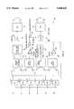
- FIG. 1ais a top view of an object position sensor transducer according to a presently preferred embodiment of the invention showing the object position sensor surface layer including a top conductive trace layer and conductive pads connected to a bottom trace layer.
- FIG. 1bis a bottom view of the object position sensor transducer of FIG. 1 a showing the bottom conductive trace layer.
- FIG. 1cis a composite view of the object position sensor transducer of FIGS. 1a and 1b showing both the top and bottom conductive trace layers.
- FIG. 1dis a cross-sectional view of the object position sensor transducer of FIGS. 1a-1c.
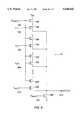
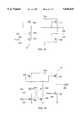
- FIG. 2is a block diagram of sensor decoding electronics which may be used with the sensor transducer in accordance with a first embodiment of the present invention.
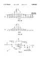
- FIGS. 3a and 3bare graphs of output voltage versus matrix conductor position which illustrate the effect of the minimum detector.
- FIG. 4is a simplified schematic diagram of an integrating charge amplifier circuit suitable for use in the present invention.
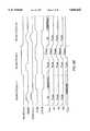
- FIG. 5is a timing diagram showing the relative timing of control signals used to operate the object position sensor system of the present invention with an integrating charge amplifier as shown in FIG. 4.
- FIG. 6ais a schematic diagram of a first alternate embodiment of an integrating charge amplifier circuit suitable for use in the present invention including additional components to bring the circuit to equilibrium prior to integration measurement.
- FIG. 6bis a timing diagram showing the control and timing signals used to drive the integrating charge amplifier of FIG. 6a and the response of various nodes in the amplifier to those signals.
- FIG. 7ais a schematic diagram of a second alternate embodiment of an integrating charge amplifier circuit suitable for use in the present invention including additional components to bring the circuit to equilibrium prior to integration measurement.
- FIG. 7bis a timing diagram showing the control and timing signals used to drive the integrating charge amplifier of FIG. 7a and the response of various nodes in the amplifier to those signals.
- FIG. 8is a schematic diagram of a minimum detector circuit according to a presently preferred embodiment of the invention.
- FIG. 9is a schematic diagram of a maximum detector circuit according to a presently preferred embodiment of the invention.
- FIG. 10is a schematic diagram of a linear voltage-to-current converter circuit according to a presently preferred embodiment of the invention.
- FIG. 11is a schematic diagram of a position encoder centroid computing circuit according to a presently preferred embodiment of the invention.
- FIG. 12is a schematic diagram of a Z Sum circuit according to a presently preferred embodiment of the invention.
- FIG. 13is a schematic diagram of a multiplier circuit according to a presently preferred embodiment of the invention.
- FIG. 14is a schematic diagram of a combination driving-point impedance circuit and receiving-point impedance circuit according to a presently preferred position matrix embodiment of the invention.
- FIG. 15is a block diagram of a structure of a portion of a sample/hold array suitable for use in the present invention.
- FIG. 16ais a block diagram of a simple version of a position matrix embodiment of the present invention in which the matrix of voltage information is sent to a computer which processes the data.
- FIG. 16bis a block diagram of a second version of a position matrix embodiment of the present invention employing a sample/hold array such as that depicted in FIG. 15.
- the present inventionbrings together in combination a number of unique features which allow for new applications not before possible. Because the object position sensor of the present invention has very low power requirements, it is beneficial for use in battery operated or low power applications such as lap top or portable computers. It is also a very low cost solution, has no moving parts (and is therefore virtually maintenance free), and uses the existing printed circuit board traces for sensors.
- the sensing technology of the present inventioncan be integrated into a computer motherboard to even further lower its cost in computer applications. Similarly, in other applications the sensor can be part of an already existent circuit board.
- the sensor technology of the present inventionis useful in lap top or portable applications where volume is important consideration.
- the sensor technology of the present inventionrequires circuit board space for only a single sensor interface chip that can interface directly to a microprocessor, plus the area needed on the printed circuit board for sensing.
- the sensor materialcan be anything that allows creation of a conductive X/Y matrix of pads. This includes not only standard PC board, but also flexible PC board, conductive elastomer materials, and piezo-electric Kynar plastic materials. This renders it useful as well in any portable equipment application or in human interface where the sensor needs to be molded to fit within the hand.
- the sensorcan be conformed to any three dimensional surface. Copper can be plated in two layers on most any surface contour producing the sensor. This will allow the sensor to be adapted to the best ergonomic form needed for a particular application. This coupled with the "light-touch" feature will make it effortless to use in many applications.
- the sensorcan also be used in an indirect manner, i.e. it can have a conductive foam over the surface and be used to detect any object (not just conductive) that presses against it's surface.
- Small sensor areasare practical, i.e., a presently conceived embodiment takes about 1.5" ⁇ 1.5" of area, however those of ordinary skill in the art will recognize that the area is scalable for different applications.
- the matrix areais scaleable by either varying the matrix trace spacing or by varying the number of traces. Large sensor areas are practical where more information is needed.
- the sensor technology of the present inventionalso provides finger pressure information.
- This additional dimension of informationmay be used by programs to control special features such as "brush-width" modes in Paint programs, special menu accesses, etc., allowing provision of a more natural sensory input to computers.
- the userwill not even have to touch the surface to generate the minimum reaction. This feature can greatly minimize user strain and allow for more flexible use.
- the sense system of the present inventiondepends on a transducer device capable of providing position and pressure information regarding the object contacting the transducer.
- a transducer devicecapable of providing position and pressure information regarding the object contacting the transducer.
- FIGS. 1a-1dtop, bottom, composite, and cross-sectional views, respectively, are shown of a presently-preferred touch sensor array for use in the present invention. Since capacitance is exploited by this embodiment of the present invention, the sensor surface is designed to maximize the capacitive coupling between top (X) trace pads to the bottom (Y) trace pads in a way that can be maximally perturbed and coupled to a finger or other object placed above the surface.
- a presently preferred sensor array 10comprises a substrate 12 including a set of first conductive traces 14 disposed on a top surface 16 thereof and run in a first direction to comprise rows of the sensor array 10.
- a set of second conductive traces 18are disposed on a bottom surface 20 thereof and run in a second direction preferably orthogonal to the first direction to form the columns of the sensor array 10.
- the sets of first and second conductive traces 14 and 18are alternately in contact with periodic sense pads 22 comprising enlarged areas, shown as diamonds in FIGS. 1a-1c. While sense pads 22 are shown as diamonds in FIGS. 1a-1c, any shape, such as circles, which allows close packing of the sense pads 22, is equivalent for purposes of this invention.
- sense pads 22The number and spacing of these sense pads 22 depends upon the resolution desired. For example, in an actual embodiment constructed according to the principles of the present invention, a 0.10 inch center-to-center diamond-shaped pattern of sense pads disposed along a matrix of 15 rows and 15 columns of conductors is employed. Every other sense pad 22 in each direction in the pad pattern is connected to sets of first and sceond conductive traces 14 and 18 on the top and bottom surfaces 16 and 20, respectively of substrate 12.
- Substrate 12may be a printed circuit board, a flexible circuit board or any of a number of available circuit interconnect technology structures. Its thickness is unimportant as long as contact may be made therethrough from the set of second conductive traces 18 to their sense pads 22 on the top surface 16.
- the printed circuit board comprising substrate 12can be constructed using standard industry techniques. Board thickness is not important. Pad-to-pad spacing should preferably be minimized to something in the range of about 15 mils or less. Connections from the sense pads 22 to the set of second traces 18 may be made employing standard plated-through hole techniques well known in the printed circuit board art.
- Insulating layer 24is disposed over the sense pads 22 on top surface 16 to insulate a human finger or other object therefrom.
- Insulating layer 24is preferably a thin layer (i.e., approximately 5 mils) to keep capacitive coupling large and may comprise a material, such as mylar, chosen for its protective and ergonomic characteristics.
- the first capacitive effectis trans-capacitance, or coupling between sense pads 22, and the second capacitive effect is self-capacitance (ground capacitance), or coupling to earth-ground.
- Sensing circuitryis coupled to the sensor array 10 of the present invention and responds to changes in either or both of these capacitances. This is important because the relative sizes of the two capacitances change greatly depending on the user environment.
- the ability of the present invention to detect changes in both self capacitance and trans-capacitanceresults in a very versatile system having a wide range of applications.
- a position sensor systemincluding sensor array 10 and associated touch detector circuitry will detect a finger position on a matrix of printed circuit board traces via the capacitive effect of finger proximity to the sensor array 10.
- the position sensor systemwill report the X, Y position of a finger placed near the sensor array 10 to much finer resolution than the spacing between the sets of first and second traces 14 and 18.
- the position sensor according to this embodiment of the inventionwill also report a Z value proportional to the outline of that finger and hence indicative of the pressure with which the finger contacts the surface of insulating layer 24 over the sensor array 10.
- a very sensitive, light-touch detector circuitmay be provided using adaptive analog VLSI techniques.
- the circuit of the present inventionis very robust and calibrates out process and systematic errors.
- the detector circuit of the present inventionwill process the capacitive input information and provide digital information to a microprocessor.
- sensing circuitryis contained on a single sensor processor integrated circuit chip.
- the sensor processor chipcan have any number of X and Y "matrix" inputs. The number of X and Y inputs does not have to be equal.
- the Integrated circuithas a digital bus as output.
- the sensor array 10has 15 traces in both the Y and Y directions.
- the sensor processor chipthus has 15 X inputs and 15 Y inputs.
- the X and Y matrix nodesare successively scanned, one at a time, with the capacitive information from that scan indicating how close a finger is to that node.
- the scanned informationprovides a profile of the finger proximity in each dimension.
- the profile centroidis derived in both the X and Y directions and is the position in that dimension.
- the profile curve of proximityis also integrated to provide the Z information.
- FIG. 2a block diagram of presently preferred sensing circuitry 30 for use according to the present invention is shown.
- the sensing circuitry 30 of this embodimentemploys a driving-point capacitance measurement for each X and Y line in the sensor array 10.
- the block diagram of FIG. 2illustrates the portion of the sensing circuitry 30 for developing signals from one direction (shown as X in the matrix).
- the circuitry for developing signals from the other direction in the matrixis identical and its interconnection to the circuitry shown in FIG. 2 will be disclosed herein.
- the sensing circuitry 30 of FIG. 2illustratively discloses an embodiment in which information from six X matrix lines X1 . . . X6 are processed.
- this embodimentis illustrative only, and that actual embodiments fabricated according to the present invention may employ an arbitrarily sized matrix, limited only by technology constraints.
- the driving-point capacitance measurement for each of X lines X1 . . . X6is derived from an integrating charge amplifier circuit. These circuits are shown in block form at reference numerals 32-1 through 32-6. The function of each of integrating charge amplifier 32-1 through 32-6 is to develop an output voltage proportional to the capacitance sensed on its corresponding X matrix line.
- the driving-point capacitance measurementis made for all X (row) first conductive traces 14 and all Y (column) second conductive traces 18 in the sensor matrix array 10.
- a profile of the finger proximity mapped into the X and Y dimensionis generated from the driving-point capacitance measurement data. This profile is then used to determine a centroid in both dimensions, thereby determining the X and Y position of the finger.
- Bus 34is a six conductor bus, and those of ordinary skill in the art will recognize that each of its conductors comprises the output of one of integrating charge amplifiers 32-1 through 32-6.
- linear voltage-to-current converter 36The first of circuit elements driven by the outputs of integrating charge amplifier circuits 32-1 through 32-6 is linear voltage-to-current converter 36.
- the function of linear voltage-to-current converter 36is to convert the output voltages of integrating charge amplifiers 32-1 through 32-6 to currents for subsequent processing.
- the current outputs from linear voltage-to-current converter 36are presented as inputs to X position encode circuit 38.
- the function of X position encode circuit 38is to convert the input information into a signal representing object proximity in the X dimension of the sensor array 10.
- this circuitwill provide a scaled weighted mean (centroid) of the set of input currents.
- the resultis a circuit which is a linear position encoder, having an output voltage which varies between the power supply rails. Because it is a weighted mean, it averages all current inputs and can in turn generate an output voltage which represents an X position with a finer resolution than the spacing of the X matrix grid spacing.
- sample/hold circuit 40The output voltage of X position encode circuit 38 is presented to sample/hold circuit 40, the output of which, as is well known in the art, either follows the input or holds a value present at the input depending on the state of its control input 42.
- sample/hold circuit 40The structure and operation of sample/hold circuits are well known in the art.
- sample/hold circuit 40drives the input of analog-to-digital (A/D) converter 44.
- A/Danalog-to-digital
- ND converter 44is a digital value proportional to the position of the object in the X dimension of the sensor array 10.
- circuit elementsWhile the portion of the circuit described so far is useful for providing a digital signal indicating object position in one dimension, the addition of further circuit elements yields a more useful device which is more immune to noise, detects and subtracts the no-object-proximate signal from the outputs of the sensors, and provides threshold detection of an approaching object.
- minimum detector circuit 46The first of these additional circuit elements is minimum detector circuit 46.
- the function of minimum detector circuit 46is to determine the level of signal representing ambient no-object-proximate to the sensor array 10 and to provide a signal which may be fed back to integrating charge amplifiers 32-1 through 32-6 to control their output voltages to effectively zero out the outputs of the integrating charge amplifiers 32-1 through 32-6 under the ambient condition.
- the output of minimum detector circuit 46is a voltage. This voltage is compared in operational amplifier 48 with an adjustable voltage representing a minimum threshold value V Thmin . Through feedback to the integrating charge amplifiers 32-1 through 32-6, operational amplifier 48 adjusts its output to balance the output voltage of minimum detector circuit 46 with the voltage V Thmin . Feedback is controlled by P-channel MOS transistor 50, which allows the feedback to operate only when the PROCESS signal is active.
- FIGS. 3a and 3bare graphs of output voltage versus matrix conductor position which illustrate the effect of the minimum detector circuit 46.
- FIGS. 3a and 3bshow the outputs of integrating charge amplifiers from a fifteen row matrix, rather than from a six row matrix as is implied by FIG. 2.
- FIG. 3ashows the offset component of the voltage outputs of integrating charge amplifiers without the operation of minimum detector circuit 46
- FIG. 3bshows the voltage outputs with the offset having been zeroed out by the feedback loop comprising minimum detector circuit 46, P-channel MOS transistor 50, and feedback conductor 52.
- maximum detector circuit 54Another additional circuit component is maximum detector circuit 54.
- the function of maximum detector circuit 54, working in co-operation with amplifier 56, OR gate 58, and AND gate 60is to provide a MAX INTERRUPT signal.
- the MAX INTERRUPT signalalerts the microprocessor controlling the object sensor system of the present invention that an object is approaching the sensor array 10.
- the amplifier 56acts as a comparator which trips if the output voltage from maximum detector circuit 54 exceeds the threshold set by the voltage V Thmax .
- the output of OR gate 58becomes true. That and a true SAMPLE signal at the second input of AND gate 60 causes a true MAX INTERRUPT signal at its output.
- the Z Sum circuit 62produces an output which is proportional to the pressure with which a finger is pressing on the sensor. This is done In both the X and Y dimensions by effectively integrating the areas under the curves of FIG. 3b. Referring again to FIG. 3b for illustration purposes, it can be seen that the width of the contact area in the X dimension of the sensor array 10 is from about X 2 to X 10 .
- Z Sum circuit 62is configured to produce an output voltage V O .
- Output voltage V Ois a scaled function of all the input voltages.
- the area of the finger or other flexible objectis a reliable measure of the pressure with which the finger is contacting the surface of the sensor array 10.
- the areamay be calculated by multiplier circuit 64, having the output of the Z Sum circuit 62 in the X dimension as one of its inputs and the output of the Z Sum circuit 62 in the Y dimension as the other one of its inputs.
- multiplier circuit 64takes two analog voltage inputs and performs an analog computation on those voltages to create a voltage output which is proportional to the product of the two input voltages.
- a first input termis the output voltage of the X dimension Z Sum circuit 62 and a second input term is the output of the Y dimension Z Sum circuit (not shown).
- Those of ordinary skill in the artwill recognize that since multiplication is commutative process and since the multiplier inputs are symmetrical, it does not matter which of the X and Y Z sum circuits 62 contributes the first input term and which contributes the second input term.
- the output of multiplier circuit 64is a voltage and drives a sample/hold circuit 66.
- Sample/hold circuit 66may be identical to sample/hold circuit 40 and may be driven by the same SAMPLE signal which drives sample/hold circuit 40.
- sample/hold circuit 66drives the input of analog-to-digital (A/D) converter 68.
- ND converter 68may be identical to A/D converter 44.
- the output of A/D converter 68is a digital value proportional to the pressure with which the finger (or other flexible object) is contacting the surface of sensor array 10.
- the object position sensor system of the present inventionmay be operated under the control of a microprocessor which provides the timing and other control signals necessary to operate the system.
- a microprocessorwhich provides the timing and other control signals necessary to operate the system.
- the MAX INTERRUPT signal from the output of AND gate 60may be used to interrupt the microprocessor and invoke an object sensing routine.
- the particular timing and control signals employed by any system constructed according to the present inventionwill vary according to the individual design. The following is therefore an illustrative disclosure providing circuit details of illustrative circuit components of a presently preferred system according to the present invention and including disclosure of typical timing and control signals for operating these circuits.
- Integrating charge amplifier 70is derived from the common integrating amplifier seen in the literature, for example in Gregorian and Temes, Analog MOS Integrated Circuits, John Wiley & Sons (1986) pp. 270-271; Haskard and May, Analog VLSI Design, Prentice Hall (1988), pp. 105-106, and is built around amplifying element 72, which may comprise a common transconductance amplifier as described in Mead, Analog VLSI and Neural Systems, Addison-Wesley (1989) pp. 70-71.
- the inverting input of amplifying element 72is connected to an input node 74 through a switch 76 controlled by a SELECT(n) node 78.
- the input node 74is connected to one of the lines in the sensor array 10 of FIG. 1. While the disclosure herein illustrates the use of an integrating charge amplifier connected to a row line of the sensor array, those of ordinary skill in the art will recognize that the operation of the integrating charge amplifiers connected to the column lines of the sensor array is identical.
- capacitor 82is connected as an integrating feedback element between the output and inverting input of amplifying element 72. According to a presently preferred embodiment of the invention, capacitor 82 may have a capacitance of about 10 pF.
- the output of amplifying element 72is connected to an output node 84 through a switch 86.
- Switch 86is controlled by the SELECT(n) node 78 which also controls switch 76.
- a capacitor 88which may have a capacitance of about 3 pF, is connected between output node 84 and an offset adjust node 90.
- switches 76 and 86may comprise common CMOS pass gates, each including an N-channel and a P-channel MOS transistor connected in parallel with their gates driven by complimentary signals.
- the combination of switch 86 and capacitor 88form a simple sample/hold circuit the offset of which may be adjusted when the switch 86 is in its off position via the voltage on offset adjust node 90.
- Amplifying element 72also includes a BIAS input node 92, which may be connected to an on-chip current bias reference which may be used for all of the integrating charge amplifiers on the chip.
- a driving-point capacitance measurementis made by closing switches 76 and 86 and stepping, by an amount Vstep, the input voltage on Voltage step input node 80 at the non-inverting input of amplifying element 72. Because of the negative feedback arrangement, the output of amplifying element 72 will then move to force the voltage at its inverting input to match the voltage at its non-inverting input. The result is that the voltage at the output node 84 changes to a value that injects enough charge into capacitor 82 to match the charge that is injected into the capacitance on the sensor array 10 line connected to input node 74. This change may be expressed as:
- V outis the output voltage
- C matrixis the capacitance on the row or column line of the sensor array 10 to which input node 74 is connected and C 82 is capacitor 82.
- Voutwill also increase in a driving-point capacitance measurement made as the finger approaches.
- V outis proportional to the proximity of a finger (conductive object) to the sensor array 10 line connected to input node 74.
- the driving-point capacitance measurementgives an output voltage change that is directly proportional to the sensor array 10 capacitance that is to be measured.
- this subtraction operationmay be performed by applying an offset adjust voltage to capacitor 88 at offset adjust node 90.
- This voltagemay be presented to the amplifier circuit via line 52 (FIG. 2) and is controlled by the Minimum Detect circuit 46 when the PROCESS control line is active.
- the offset adjust node 90subtracts the "no object voltage" from the output node 84 and leaves an output voltage directly proportional to the change of the capacitance at the row line of the sensor array 10 to which input node 74 is connected caused by the approaching object.
- the integrating charge amplifiers 70are selected one at a time using their select nodes 78. This closes both switches 76 and 86 to start the integrator and to start sampling the results of this operation.
- the voltage at the Voltage step input node 80is stepped, and the circuit is allowed to settle. After sufficient settling time the select signal is disabled, switches 76 and 86 are opened and the sampled result is left stored at the output node 84 on capacitor 88.
- FIG. 5a timing diagram shows the relationship between the timing and control signals used to operate the object position sensor system of the present invention utilizing the integrating charge amplifier 70 of FIG. 4.
- first all X and Y integrating charge amplifiersare sequentially selected, followed by a PROCESS signal and then a SAMPLE signal.
- FIG. 6ain an alternate embodiment of an integrating charge amplifier 100, all components of the embodiment of FIG. 4 are present.
- the portion of the cycle in which a global RESET node is trueis used to equibrilate the circuit by discharging the integrating feedback capacitor 82 to zero volts.
- the voltage V STEPis then provided to the non-inverting input of the amplifying element 72 in a manner which allows easily controlled stepping between the two designated voltages, V LOW and V HIGH .
- the additional components in integrating charge amplifier 100include a switch 102 connected across capacitor 82 connected to a RESET node 104 connected to all of the integrating charge amplifiers 100 in the system.
- switch 102turns on and discharges the capacitor 82 to zero volts.
- a switch 106is connected between the input node 74 and ground has a control element connected to a RESET1 (n) node 108.
- the RESET1 (n) node 108is active for all integrating charge amplifiers except for the one selected by its SELECT(n) node to perform the driving-point impedance measurement. Its function is to discharge any voltage present on those nodes due to the capacitive coupling to the other nodes which have been driven by the scanning process and thereby eliminate or minimize the error which such voltages would introduce into the measurement process.
- the V STEP voltagemay be provided to the non-inverting input of amplifying element 72 by employing switches 110 and 112.
- Switch 110is connected between a V HIGH voltage node 114 and the non-inverting input of amplifying element 72, and is controlled by a STEP node 116.
- Switch 112is connected between a V LOW voltage node 118 and the non-inverting input of amplifying element 72, and is controlled by a STEP node 120.
- Switches 102, 106, 110, and 112may comprise common CMOS pass gates.
- FIG. 6ba timing diagram shows the relationships between the various control signals and the voltages present on selected nodes of the integrating charge amplifier 100 of FIG. 6a during scan cycles (n-1), (n), and (n+1).
- the global RESET signal at RESET node 104discharges the capacitors 82 of all integrating charge amplifiers 100 in the system at the beginning of each scanning cycle.
- the RESET1(n) signal at RESET1(n) node 108is coincident with the RESET signal during scanning cycles (n-1) and (n+1) but does not appear at the RESET1(n) node 108 of the integrating charge amplifier 100 which is making the driving-point capacitance measurement during scanning cycle (n).
- FIG. 6balso shows the STEP and STEP signals drive the non-inverting input of amplifying element 72 first to V LOW and then to V HIGH during each scanning cycle.
- the signals N1, N2, and N3represent the voltages present at the inverting input, the non-inverting input, and the output, respectively, of amplifying element 72.
- the voltage V measthe voltage of interest, remains at the output node of integrating charge amplifier 100 even after the end of scan cycle (n) in which it was developed.
- an embodiment of an integrating charge amplifier 130is an approach that provides a larger operating range for the integration.
- the embodiment of FIG. 7ais nearly identical in its structure and operation to the embodiment of FIG. 6a, except that instead of switch 102 acting to discharge capacitor 82 to zero volts when the RESET node 104 is true, switch 132, which may comprise a common CMOS pass gate, is used to force the output of amplifying element 72 to ground (zero volts) instead of to V LOW as in the embodiment of FIG. 6a.
- a switch 134also controlled by RESET node 104, is used to short together the inverting and non-inverting inputs of amplifying element 72, forcing them both to an equilibrium voltage of V LOW . In low power supply-voltage applications, such as found in notebook computers, this circuit increases the signal sensitivity by a factor of two.
- FIG. 7bis a timing diagram which shows the relationships between the various control signals and the voltages present on selected nodes of the integrating charge amplifier circuit 130 of FIG. 7a during scan cycles (n-1), (n), and (n+1).
- the global RESET signal at node 104forces the outputs of all integrating charge amplifiers 130 in the system to zero volts at the beginning of each scanning cycle.
- the RESET1(n) signal at RESET1(n) node 108is coincident with the RESET signal during scanning cycles (n-1) and (n+1) but does not appear at the RESET1(n) node 108 of the integrating charge amplifier 130 which is making the driving-point capacitance measurement during scanning cycle (n).
- the STEP and STEP signalsdrive the non-inverting input of amplifying element 72 first to V LOW and then to V HIGH during each scanning cycle.
- the signals N1, N2, and N3represent the voltages present at the inverting input, the non-inverting input, and the output, respectively, of amplifying element 72.
- the voltage V measthe voltage of interest, remains at the output node of integrating charge amplifier 130 even after the end of scan cycle (n) in which it was developed.
- FIG. 8a schematic diagram is presented of a minimum detector circuit 46 of FIG. 2. While the X dimension minimum detector circuit 46 is illustratively disclosed herein, those of ordinary skill in the art will understand that the Y dimension minimum detector circuit functions in the same manner.
- minimum detector circuit 46includes a P-channel MOS bias transistor 142 having its source connected to a voltage source V DD and its gate connected to a bias voltage V BIAS .
- the inputs of the minimum detector circuit 46are connected to the output nodes 84 of the respective integrating charge amplifiers.
- Each input sectioncomprises a series pair of MOS transistors connected between the drain of P-channel MOS bias transistor 142 and ground.
- the input section for In 1comprises P-channel MOS input transistor 144 having its source connected to the drain of P-channel MOS bias transistor 142 and N-channel MOS current-limiting transistor 146 having its drain connected to the drain of P-channel MOS input transistor 144 and its source connected to ground.
- the gate of P-channel MOS input transistor 144is connected to In 1 input node 148 and the gate of N-channel MOS current-limiting transistor 146 is connected to a source of limiting bias voltage V LBIAS at node 150.
- the input section for In 2comprises P-channel MOS input transistor 152 having its source connected to the drain of P-channel MOS bias transistor 142 and N-channel MOS current-limiting transistor 154 having its drain connected to the drain of N-channel MOS input transistor 152 and its source connected to ground.
- the gate of P-channel MOS input transistor 152is connected to In 2 input node 156 and the gate of N-channel MOS current-limiting transistor 154 is connected to node 150.
- the input section for In 3comprises P-channel MOS input transistor 158 having its source connected to the drain of P-channel MOS bias transistor 142 and N-channel MOS current-limiting transistor 160 having its drain connected to the drain of P-channel MOS input transistor 158 and its source connected to ground.
- the gate of P-channel MOS input transistor 158is connected to In 3 input node 162 and the gate of N-channel MOS current-limiting transistor 160 is connected to node 150.
- the input section for In.sub.(n)comprises P-channel MOS input transistor 164 having its source connected to the drain of P-channel MOS bias transistor 142 and N-channel MOS current-limiting transistor 166 having its drain connected to the drain of P-channel MOS input transistor 164 and its source connected to ground.
- the gate of P-channel MOS input transistor 164is connected to In.sub.(n) input node 168 and the gate of N-channel MOS current-limiting transistor 146 is connected to node 150.
- the output of minimum detector circuit 46is node 170.
- V BIAS and V LBIASwould be set so that the saturation currents in any one of transistors 146, 154, 160 N-channel MOS current-limiting . . . 166 is much larger than the saturation current in P-channel MOS bias transistor 142.
- In1is the smallest voltage of all n inputs.
- P-channel MOS input transistor 144is turned on strongly with N-channel MOS current-limiting transistor 146 taking all the current from P-channel MOS bias transistor 142.
- output node 170moves down until P-channel MOS input transistor 144 is on just enough to sink all the current from P-channel MOS bias transistor 142.
- the minimum detector circuit 46 of FIG. 8in an averaging mode provides substantial noise rejection in the system. If for some reason one input was noisy and gave a much smaller value than all other values it could cause the generation of an erroneous output voltage. According to the present invention, the goal is to detect the "background level" of an input with no input stimulus. This would be the true minimum value. Since there are typically more than one input in this state, several inputs can be averaged to form the minimum signal. This is done via the averaging mode, which is enabled by setting the V LBIAS current of each N-channel MOS current-limiting transistor 146, 154, 160 . . . 166 to be some fraction of the current from P-channel MOS bias transistor 142.
- the current set by V LBIASis approximately one-third of the current from P-channel MOS bias transistor 142. Therefore, in order to sink all of the current from P-channel MOS bias transistor 142, at least three input P-channel MOS input/N-channel MOS current-limiting transistor pairs (144/146 . . . 164/166) must be turned on. For that to happen the output node 170 must then be sitting at a voltage equal to a P-channel bias voltage above the third lowest input. It has thus, in effect, filtered out and ignored the two lower values.
- the present embodiment of the minimum detect circuit of FIG. 8has been described in terms of separately deriving an X minimum signal and a Y minimum signal and separately computing their weighted minima. Those of ordinary skill in the art will recognize that, pursuant to an equivalent embodiment, the weighted minima of the combined X and Y signals could be computed utilizing the principles disclosed herein.
- operational amplifier 48(a transconductance amplifier operating as a comparator) and the bottom of capacitor 88 in the integrating charge amplifiers 70, 100, and 130 of FIGS. 4, 6a, and 7a has been held high by P-channel MOS transistor 50 during the scan operation or non-PROCESS cycles when the global PROCESS signal (FIG. 5) is low.
- the PROCESS cyclestarts, the PROCESS line goes high and P-channel MOS transistor 50 is turned off, thus enabling the action of minimum detector circuit 46. If the output of minimum detector circuit 46 is greater than the V Thmin at the input of operational amplifier 48, the output of operational amplifier 48 is driven low.
- the V Thmin voltageis chosen so that when the integrating charge amplifiers (32-1 through 32-6) outputs are shifted down, the minimum charge amplifier output will generate no current in the voltage-to-current converter circuits 36.
- maximum detector circuit 54includes an N-channel bias transistor 182 having its source connected to ground and its gate connected to a bias voltage V BIAS at node 184.
- the inputs of the maximum detector circuit 54are connected to the output nodes 84 of the respective integrating charge amplifiers 70, 100 and 130.
- Each input sectioncomprises a series pair of MOS transistors connected between the drain of N-channel bias transistor 182 and a voltage source V DD .
- the input section for In 1comprises P-channel MOS current-limiting transistor 186 having its source connected to V DD and its drain connected to the drain of N-channel MOS input transistor 188.
- the gate of N-channel MOS input transistor 188is connected to In 1 input node 190 and the gate of P-channel MOS current-limiting transistor 186 is connected to a source of bias voltage V LBIAS at node 192.
- the input section for In 2comprises P-channel MOS current-limiting transistor 194 having its source connected to V DD and its drain connected to the drain of N-channel MOS input transistor 196.
- the gate of N-channel MOS input transistor 196is connected to In 2 input node 198 and the gate of P-channel MOS current-limiting transistor 194 is connected to node 192.
- the input section for In 3comprises P-channel MOS current-limiting transistor 200 having its source connected to VDD and its drain connected to the drain of N-channel MOS input transistor 202.
- the gate of N-channel MOS input transistor 202is connected to In 3 input node 204 and the gate of P-channel MOS current-limiting transistor 200 is connected to node 192.
- the input section for In(n)comprises P-channel MOS current-limiting transistor 206 having its source connected to VDD and its drain connected to the drain of N-channel MOS input transistor 208.
- N-channel MOS input transistor 208is connected to In.sub.(n) input node 210 and the gate of N-channel MOS current-limiting transistor 206 is connected to node 192.
- the sources of N-channel MOS input transistors 188, 198, 202, and 208are connected together to the drain of N-channel MOS bias transistor 182.
- the output of maximum detector circuit 54is node 212 at the common connection of the drain of N-channel bias transistor 182 and the sources of the N-channel input transistors 188, 196, 202 and 208.
- the maximum detector circuit 54acts analogously to the minimum detector circuit 46.
- the differenceis that an N-channel bias transistor is used instead of a P-channel bias transistor and an N-channel transconductance amplifier is used in place of a P-channel transconductance amplifier.
- the resultis the output will now track approximately an N-channel bias drop below the largest input (in non-averaging mode), since that much difference is needed to guarantee at least one input P-channel MOS current-limiting/N-channel MOS input transistor pair (186/188, 194/196 . . . 206/208) is on.
- the outputis not used for feedback, but is instead used to drive a amplifier comparator 56 (FIG. 2) which is set to trip if the input is greater than the voltage V Thmax . If tripped, a MAX INTERRUPT signal is generated.
- the MAX INTERRUPTis used to "wake-up" a microprocessor and tell it that there is an object detected at the sensor. The signal is prevented from appearing on the MAX INTERRUPT line by gate AND gate 60 and the SAMPLE signal. The SAMPLE signal only allows the interrupt signal to pass after the circuit has settled completely.
- OR gate 58either the X or the Y dimension maximum detector circuit 54 may be used to enable the MAX INTERRUPT signal.
- FIG. 10a presently preferred embodiment of linear voltage-to-current circuit converter 36 is shown in schematic form.
- block 36 in FIG. 2actually contains one voltage to current converter circuit of FIG. 10 for each output of an integrating charge amplifier.
- a current mirrorcomprises diode-connected P-channel MOS transistor 222 having its source connected to voltage source V DD , and P-channel MOS transistor 224 having its source connected to voltage source V DD and its gate connected to the gate and drain of P-channel MOS transistor 222.
- An N-channel MOS input transistor 226has its drain connected to the drain of P-channel MOS transistor 222, its gate connected to a voltage input node 228, and its source connected to the drain of N-channel MOS bias transistor 230.
- the source of N-channel MOS bias transistor 230is connected to ground and its gate is connected to bias input 232.
- the drain of P-channel MOS transistor 224is connected to the gate and drain of diode connected N-channel MOS transistor 234.
- the source of diode connected N-channel MOS transistor 234is connected to ground.
- the common gate and drain connection of diodeconnected N-channel MOS transistor 234is an N Bias current output node 238 and the common connection of the gate of P-channel MOS transistor 224 and the drain of P-channel MOS transistor 222 is a P Bias current output node 236 of the voltage-to-current-converter 36.
- N-channel MOS bias transistor 230is biased in its linear region by setting V BIAS to be a value which is much greater than the largest value expected on the voltage input node 228. This will guarantee it is always operating in its linear region.
- V BIASthe voltage to be expected at the voltage input node 228 of the voltage-to-current converter 36 is typically less than half of the power supply, so it will operate linearly if V BIAS is set to the power supply or greater.
- N-channel MOS input transistor 226The transconductance of N-channel MOS input transistor 226 is designed to be as large as reasonable. The result is that N-channel MOS input transistor 226 will operate like a follower with a resistor in its source, and hence will give a linear change of output current versus a linear change in input voltage.
- the currentis sourced by diode-connected P-channel MOS transistor 222 which acts as half of a CMOS P-channel current mirror and provides a reference for P Bias Output node 236 for the position encode circuit 38 shown in FIG. 2.
- the currentis mirrored thru P-channel MOS transistor 224 and diode connected N-channel MOS transistor 234 generating a reference at N Bias output node 238 for the position encode circuit 38.
- the linear voltage-to-current converter 36 of FIG. 10is disclosed in U.S. Pat. No. 5,096,284 operating in the weak inversion region. This circuit is used in the strong inversion region in the present invention, however, for certain applications, the weak inversion mode may be preferred.
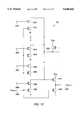
- FIG. 11a presently preferred embodiment of a position encode circuit 38 of FIG. 2 is shown in schematic diagram form.
- the circuits in the X and Y dimensionsare identical.
- the position encode circuit 38is shown having six inputs, but those of ordinary skill in the art will recognize that, due to its symmetry, it may be arbitrarily expanded.
- position encode circuit 38includes a plurality of transconductance amplifiers 242-1 through 242-6 connected as followers. The outputs of all transconductance amplifiers 242-1 through 242-6 are connected together to a common node 244, which comprises the position encode output node of the circuit 38.
- transconductance amplifiers 242-1 through 242-6are connected to a resistive voltage divider network comprising resistors 246, 248, 250, 252, 254, 256, and 258, shown connected between V DD and ground.
- Transconductance amplifiers 242-1 through 242-3have P-channel MOS bias transistors and transconductance differential pair inputs due to the input operating range between zero volts and V DD /2, and amplifiers 242-4 through 242-6 have N-channel MOS bias transistors and differential pair inputs due to the input operating range between V DD /2 and V DD .
- transconductance amplifiers 242-4 through 242-6will be configured exactly like transconductance amplifiers 242-1 through 242-3, except that all transistor and supply voltage polarities are reversed.
- the input nodes I In1 through I In6(reference numerals 260, 262, 264, 266, 268, and 270) of the circuit are connected to the gates of the MOS bias transistors of the transconductance amplifiers 242-1 through 242-6, respectively.
- the inputs I In1 through I In3are driven by the P Bias output nodes 236 of their respective linear voltage-to-current converters and the inputs I In4 through I In6 are driven by the N Bias output nodes 238 of their respective linear voltage-to-current converters.
- the position encode circuit 38 of FIG. 11will provide a weighted mean (centroid) of the input currents weighted by the voltages on the resistor divider circuit to which the inputs of the amplifiers 242-1 through 242-6 are connected. If the transconductance resistors 246, 248, 250, 252, 254, 256, and 258 are all equal then the result is a circuit which is a linear position encoder, with its output voltage varying between the power supply rails. Because it is a weighted mean, it averages all current inputs which in turn generates an interpolated output. This arrangement affords finer resolution than the voltage spacing of voltage nodes "n" at the input. This is key to making a dense circuit function. This circuit is an improvement of a circuit described in DeWeerth, Stephen P., Analog VLSI Circuits For Sensorimotor Feedback, Ph.D Thesis, California Institute of Technology, 1991.
- Z Sum circuit 62is shown to include four inputs. Those of ordinary skill in the art will readily understand how to provide additional inputs.
- the four input sections for the Z Sum circuit 62 illustrated in FIG. 12each comprise two N-channel MOS transistors connected in series.
- a first input sectioncomprises N-channel MOS input transistor 290, having its drain connected to the drain of P-channel MOS bias transistor 282 and its source connected to the drain of N-channel MOS transistor 292.
- the gate of N-channel MOS input transistor 290is connected to input node In 1 at reference numeral 294.
- the gate of N-channel MOS bias transistor 292is connected to bias input node 296.
- a second input sectioncomprises N-channel MOS input transistor 298, having its drain connected to the drain of P-channel MOS bias transistor 282 and its source connected to the drain of N-channel MOS transistor 300.
- the gate of N-channel MOS input transistor 298is connected to input node In 2 at reference numeral 302.
- the gate of N-channel MOS bias transistor 300is connected to bias input node 296.
- a third input sectioncomprises N-channel MOS input transistor 304, having its drain connected to the drain of P-channel MOS bias transistor 282 and its source connected to the drain of N-channel MOS transistor 306.
- the gate of N-channel MOS input transistor 304is connected to input node In 3 at reference numeral 308.
- the gate of N-channel MOS bias transistor 306is connected to bias input node 296.
- a fourth input sectioncomprises N-channel MOS input transistor 310, having its drain connected to the drain of P-channel MOS bias transistor 282 and its source connected top the drain of N-channel MOS transistor 312.
- the gate of N-channel MOS input transistor 310is connected to input node In4 at reference numeral 314.
- the gate of N-channel MOS bias transistor 312is connected to bias input node 296.
- the common drain connections of N-channel MOS input transistors 290, 298, 304, and 310are connected to the gate of P-channel MOS transistor 316.
- the Z sum circuit 62 of FIG. 12is analogous to the linear voltage-to-current converter circuit 36 of FIG. 10. However in this case there are multiple circuit sections which have their currents all summed together (N-channel MOS transistors 290/292, 298/300, 304/306 . . . 310/312) into the P-channel MOS transistor 282.
- P-channel MOS transistors 282 and 316form a current mirror. Their sources are connected to voltage source VDD and their gates are connected together to the drain P-channel MOS of transistor 282.
- the drain of P-channel MOS transistor 316is connected to the drain of N-channel MOS transistor 318, which has its source connected to ground.
- the common connection of the drains of MOS transistors 316 and 318forms a voltage output node 320 for the circuit Z sum 62.
- P-channel MOS transistor 316drives N-channel MOS transistor 318 which is operating in its linear region. The result is a voltage which is proportional to the current from N-channel MOS transistor 316. Therefore the voltage at voltage output node 320 is a scaled sum of all the input voltages, and is utilized by the multiplier circuit 64 shown in FIG. 2.
- N-channel MOS transistor 336has its drain connected to the drain of P-channel MOS transistor 332, its gate connected to first voltage input node 338, and its source connected to the drain of N-channel MOS transistor 340.
- the gate of N-channel MOS transistor 340is connected to second voltage input node 342 and its source is connected to ground.
- N-channel MOS transistor 344has its drain connected to the gate and drain of P-channel MOS transistor 332.
- the gate of N-channel MOS transistor 344is connected to second voltage input node 342 and its source is connected to the drain of N-channel MOS transistor 346.
- the gate of N-channel MOS transistor 346is connected to first voltage input node 338 and its source is connected to ground.
- the sources of P-channel MOS transistors 332 and 334are connected to voltage source V DD .
- the drain of P-channel MOS transistor 334is connected to output node 348 and to the drain of N-channel MOS transistor 350.
- the gate of N-channel MOS transistor 350is connected to input bias node 352.
- the multiplier circuit 64 of FIG. 13is a symmetrized extension of the multiplier described in U.S. Pat. No. 5,095,284 and is a wide input range, voltage-input, voltage-output multiplier circuit. Because of the symmetrical input stage, the multiplier circuit 64 can be operated both above and below the threshold voltages of transistors 340 and 346.
- N-channel MOS transistor 350is biased to be in its linear region by bias input 352. Therefore, the output voltage at output node 348 will be proportional to the conductance of N-channel MOS transistor 350 multiplied by the current driven by P-channel MOS transistor 334.
- the bias voltage at input bias node 352is adjusted to scale the range of Vout values at output node 348 and, once set, is left constant. Thereafter, the output voltage is proportional to the current injected from P-channel MOS transistor 334, and hence is proportional to the product of the two input voltages at first and second voltage input nodes 338 and 342.
- a position matrix sensing systemis disclosed herein.
- the position matrix embodiment of the present inventionis a straightforward extension of the finger position invention and uses much the same circuitry and basic signal flow. The main differences are in the measurement technique and the amount of information stored.
- the goalis to provide a matrix of voltages, V(x,y), that represent the proximity of the object to every node (x,y) on the sensor matrix.
- V(x,y)a matrix of voltages
- the informationis instead sent to the input of a neural network circuit, which uses this multi-dimensional information to help it make decisions about what the input means.
- the driving-point capacitance informationis used for position detection.
- the driving-point capacitancelooks at the total capacitive effect on the node being measured, it is incapable of resolving what is happening at each X and Y location on the sensor.
- the position matrix embodiment of the present inventionhas the capability of resolving the capacitive effect at each X and Y location of the sensor.
- the driving-point capacitance circuitis only used to inject charge into the X matrix node.
- the trans-capacitancei.e., the capacitance between a selected X node and a selected Y node in the sensor matrix
- causes some of that chargeto in turn be injected into a Y node.
- This injected chargeis measured by the charge-sensitive amplifier connected to the Y node, thus forming a receiving-point capacitance circuit.
- FIG. 14a presently preferred combination driving-point capacitance circuit and receiving-point capacitance circuit is shown in schematic diagram form.
- Transcapacitance between nodes X.sub.(n) Y.sub.(n)is represented by capacitor C XY .
- a driving-point capacitance measurementis made of row line X.sub.(n) by a circuit which, as shown, may be one of the integrating charge amplifier circuits of either FIG. 6a or FIG. 7a, equipped with switches to zero out the matrix prior to injecting charge onto the matrix. The output of this circuit need not be used for anything.
- chargeis injected into all of the Y receiving-point capacitance measuring circuits (the integrating charge amplifier). If all Y outputs are monitored simultaneously then for one X node, a profile of all the transcapacitive effects at all the Y nodes that cross it will be created as a set of voltages V(x,1), V(x,2), . .
- V(x,m)that are a profile of the object (or objects) proximity on that X node. This sequence is done for every X node in the matrix resulting in a complete matrix of voltages whose values are proportional to the proximity of nearby objects.
- the receiving-point circuitcan be an integrating charge amplifier identical to that used in the driving-point circuit.
- the V STEP nodeis left at a constant voltage, V LOW , by disabling the STEP input such that switch 112 (FIGS. 6a and 7a) is always on and switch 110 is always off.
- the Y receiving circuitsare not individually selected, but instead are all selected simultaneously. Hence, there is only one Y select line for all Y inputs.
- the RESET1 lineis not used in the receiving-point circuit, and switch 106 (FIGS. 6a and 7a) is always off.
- the position matrix embodimentrequires storage of all of the output signals from the receiving-point impedance capacitance circuits in both the X and Y directions. This may be a accomplished by providing a sample/hold circuit matrix or a charge-coupled device (CCD) array as is known in the art.
- CCDcharge-coupled device
- FIG. 15shows a portion of a sample/hold array 350 suitable for use in the present invention.
- the sample/hold array 350is arranged as a plurality of rows and columns of individual sample/hold circuits. The number of rows is equal to the number of Y positions in the sensor matrix and the number of columns is equal to the number of X positions in the sensor matrix. For example, a 15 ⁇ 15 sensor matrix requires 15 rows and 15 columns.
- All of the voltage data inputs in a roware wired together and the sample/hold control inputs of all the sample/hold circuits in a column are connected to one of the select signals (FIG. 5) such that the select inputs from the X direction drive the sample/hold circuits in the matrix storing the Y data.
- select signalsFIG. 5
- FIGS. 16a and 16btwo possible embodiments of the position matrix system of the present invention are illustrated.
- the matrix of voltage informationis sent to a computer which processes the data. This simple embodiment is shown in FIG. 16a.
- the approach of FIG. 16ais feasible if the input profile shapes change no faster than about every millisecond.
- the X dimension integrating charge amplifiers(reference numerals 362-1 through 362-n) are used to perform the driving-point capacitance measurements disclosed herein for all X lines in the matrix.
- the Y dimension integrating charge amplifiers(reference numerals 364-1 through 364-n) are used to perform the receiving-point capacitance measurements disclosed herein.
- the sample/hold matrix of FIG. 15is not required. Instead, one sample/hold amplifier (366-1 through 366-n) is required per Y output to sample the output voltages from the Y dimension integrating charge amplifiers 364-1 through 364-n at the end of each X select period.
- A/D converters 368-1 through 368-nare digitized by A/D converters 368-1 through 368-n respectively.
- the digital resolutionwill be of the order of 8 bits.
- the 8-bit data words from each ND converter 368-1 through 368-nare multiplexed down to a bus width that is more easily handled by a computer by multiplexer 370.
- Multiplexer 370is a conventional multiplexer device known to those of ordinary skill in the art.
- the output of multiplexer 370is presented to a computer which may then process the data in an appropriate manner.
- FIG. 16bA second illustrative embodiment of position matrix system (reference numeral 380) is shown in FIG. 16b.
- the X dimension integrating charge amplifiers(reference numerals 362-1 through 362-n) are used to perform the driving-point capacitance measurements disclosed herein for all X lines in the matrix.
- the Y dimension integrating charge amplifiers(reference numerals 364-1 through 364-n) are used to perform the receiving-point capacitance measurements disclosed herein.
- the sample/hold array 350 of FIG. 15is employed and describes the extraction of derivation of the n by m array of voltages applications (V(1,1) to V(n,m)). These voltages are then sent to the input of a single or multiple level neural network 382. Each input neuron will have to have n*m input nodes to support the full size of the sensor array voltage matrix V(n,m).
- the typical application of this embodimentwould require a neural network or computer program that at the primitive level can discern objects (finger touch points). This is the basic symbol, the presence of a finger, that is manipulated. From that point there may be predetermined gestures that the system looks for which indicate action. Motion may also need to be detected. A possible solution for this may be found in Mead, Analog VLSI and Neural Systems, Addison-Wesley (1989), Chapter 14, Optical Motion Sensor.
- the senor of the present inventionmay be placed in a convenient location, e.g., below the "space bar" key in a portable computer.
- a convenient locatione.g., below the "space bar” key in a portable computer.
- the thumb of the usermay be used as the position pointer on the sensor to control the cursor position on the computer screen.
- the cursormay then be moved without the need for the user's fingers to leave the keyboard.
- thisis similar to the concept of the Macintosh Power Book with its trackball, however the present invention provides a significant advantage in size over the track ball. Extensions of this basic idea are possible in that two sensors could be placed below the "space bar” key for even more feature control.
- the computer display with its cursor feedbackis one small example of a very general area of application where a display could be a field of lights or LED's, a LCD display, or a CRT. Examples include touch controls on laboratory equipment where present equipment uses a knob/button/touch screen combination. Because of the articulating ability of this interface, one or more of those inputs could be combined into one of our inputs.
- Consumer Electronic Equipmentstereos, graphic equalizers, mixers
- the present inventioncan provide such control in one small touch pad location.
- Electronic Home Systemsbecome more common, denser and more powerful human interface is needed.
- the sensor technology of the present inventionpermits a very dense control panel. Hand Held TV/VCR/Stereo controls could be ergonomically formed and allow for more powerful features if this sensor technology is used.
- the sensor of the present inventioncan be conformed to any surface and can be made to detect multiple touching points, making possible a more powerful joystick.
- the unique pressure detection ability of the sensor technology of the present inventionis also key to this application.
- Computer games, "remote” controls (hobby electronics, planes) , and machine tool controlsare a few examples of applications which would benefit from the sensor technology of the present invention.
- the sensor technology of the present inventioncan best detect any conducting material pressing against it. By adding a conductive foam material on top of the sensor the sensor of the present invention may also indirectly detect pressure from any object being handled, regardless of its electrical conductivity.
Landscapes
- Engineering & Computer Science (AREA)
- Theoretical Computer Science (AREA)
- General Engineering & Computer Science (AREA)
- Human Computer Interaction (AREA)
- Physics & Mathematics (AREA)
- General Physics & Mathematics (AREA)
- Computer Hardware Design (AREA)
- Measurement Of Length, Angles, Or The Like Using Electric Or Magnetic Means (AREA)
Abstract
Description
This is a file-wrapper continuation of patent application Ser. No. 07/895,934, filed Jun. 8, 1992 now abandoned.
1. Field of the Invention
The present invention relates to object position sensing transducers and systems. More particularly, the present invention relates to object position sensors useful in applications such as cursor movement for computing devices and other applications.
2. The Prior Art
Numerous devices are available or have been proposed for use as object position detectors for use in computer systems and other applications. The most familiar of such devices is the computer "mouse". While extremely popular as a position indicating device, a mouse has mechanical parts and requires a surface upon which to roll its position ball. Furthermore, a mouse usually needs to be moved over long distances for reasonable resolution. Finally, a mouse requires the user to lift a hand from the keyboard to make the cursor movement, thereby upsetting the prime purpose, which is usually typing on the computer keyboard.
Trackball devices are similar to mouse devices. A major difference, however is that, unlike a mouse device, a trackball device does not require a surface across which it must be rolled. Trackball devices are still expensive, have moving parts, and require a relatively heavy touch as do the mouse devices. They are also large in size and doe not fit well in a volume sensitive application like a laptop computer.
There are several available touch-sense technologies which may be employed for use as a position indicator. Resistive-membrane position sensors are known and used in several applications. However, they generally suffer from poor resolution, the sensor surface is exposed to the user and is thus subject to wear. In addition, resistive-membrane touch sensors are relatively expensive. A one-surface approach requires a user to be grounded to the sensor for reliable operation. This cannot be guaranteed in portable computers. An example of a one-surface approach is the UnMouse product by MicroTouch, of Wilmington, Mass. A two-surface approach has poorer resolution and potentially will wear out very quickly in time.
Surface Acoustic Wave (SAW) devices have potential use as position indicators, However, this sensor technology is expensive and is not sensitive to light touch. In addition, SAW devices are sensitive to residue buildup on the touch surfaces and generally have poor resolution.
Strain gauge or pressure plate approaches are an interesting position sensing technology, but suffer from several drawbacks. This approach may employ piezo-electric transducers. One drawback is that the piezo phenomena is an AC phenomena and may be sensitive to the user's rate of movement. In addition, strain gauge or pressure plate approaches are a somewhat expensive because special sensors are required,
Optical approaches are also possible but are somewhat limited for several reasons. All would require light generation which will require external components and increase cost and power drain, For example, a "finger-breaking" infra-red matrix position detector consumes high power and suffers from relatively poor resolution.
The present invention comprises a position-sensing technology particularly useful for applications where finger position information is needed, such as in computer "mouse" or trackball environments. However the position-sensing technology of the present invention has much more general application than a computer mouse, because its sensor can detect and report if one or more points are being touched. In addition, the detector can sense the pressure of the touch.
There are at least two distinct embodiments of the present invention. Both embodiments of the present invention include a sensor comprising a plurality of spaced apart generally parallel conductive lines disposed on a first surface.
According to a first embodiment of the present invention, referred to herein as a "finger pointer" embodiment, a position sensing system includes a position sensing transducer comprising a touch-sensitive surface disposed on a substrate, such as a printed circuit board, including a matrix of conductive lines. A first set of conductive lines runs in a first direction and is insulated from a second set of conductive lines running in a second direction generally perpendicular to the first direction. An insulating layer is disposed over the first and second sets of conductive lines. The insulating layer is thin enough to promote significant capacitive coupling between a finger placed on its surface and the first and second sets of conductive lines.
Sensing electronics respond to the proximity of a finger to translate the capacitance changes between the conductors caused by finger proximity into position and touch pressure information. Its output is a simple X, Y and pressure value of the one object on its surface. The matrix of conductive lines are successively scanned, one at a time, with the capacitive information from that scan indicating how close a finger is to that node. That information provides a profile of the proximity of the finger to the sensor in each dimension. The centroid of the profile is computed with that value being the position of the finger in that dimension. The profile of position is also integrated with that result providing the Z (pressure) information. The position sensor of the first embodiment of the invention can only detect the position of one object on its sensor surface. If more than one object is present, the position sensor of this embodiment tries to compute the centroid position of the combined set of objects.
According to a second embodiment of the present invention, a position sensing system includes a position sensing transducer as described herein. Sensing electronics respond to the proximity of a finger to translate the capacitance changes between the conductors running in one direction and those running in the other direction caused by finger proximity into position and touch pressure information. The sensing electronics of the second embodiment of the invention saves information for every node in its sensor matrix and can thereby give the full X/Y dimension picture of what it is sensing. It thus has much broader application for richer multi-dimensional sensing than does the first "finger pointer" embodiment. In this embodiment, referred to herein as the "position matrix" approach, the x,y coordinate information can be used as input to a on-chip neural network processor. This allows an operator to use multiple fingers, coordinated gestures, etc. for even more complex interactions.
FIG. 1a is a top view of an object position sensor transducer according to a presently preferred embodiment of the invention showing the object position sensor surface layer including a top conductive trace layer and conductive pads connected to a bottom trace layer.
FIG. 1b is a bottom view of the object position sensor transducer of FIG. 1 a showing the bottom conductive trace layer.
FIG. 1c is a composite view of the object position sensor transducer of FIGS. 1a and 1b showing both the top and bottom conductive trace layers.
FIG. 1d is a cross-sectional view of the object position sensor transducer of FIGS. 1a-1c.
FIG. 2 is a block diagram of sensor decoding electronics which may be used with the sensor transducer in accordance with a first embodiment of the present invention.
FIGS. 3a and 3b are graphs of output voltage versus matrix conductor position which illustrate the effect of the minimum detector.
FIG. 4 is a simplified schematic diagram of an integrating charge amplifier circuit suitable for use in the present invention.
FIG. 5 is a timing diagram showing the relative timing of control signals used to operate the object position sensor system of the present invention with an integrating charge amplifier as shown in FIG. 4.
FIG. 6a is a schematic diagram of a first alternate embodiment of an integrating charge amplifier circuit suitable for use in the present invention including additional components to bring the circuit to equilibrium prior to integration measurement.
FIG. 6b is a timing diagram showing the control and timing signals used to drive the integrating charge amplifier of FIG. 6a and the response of various nodes in the amplifier to those signals.
FIG. 7a is a schematic diagram of a second alternate embodiment of an integrating charge amplifier circuit suitable for use in the present invention including additional components to bring the circuit to equilibrium prior to integration measurement.
FIG. 7b is a timing diagram showing the control and timing signals used to drive the integrating charge amplifier of FIG. 7a and the response of various nodes in the amplifier to those signals.
FIG. 8 is a schematic diagram of a minimum detector circuit according to a presently preferred embodiment of the invention.
FIG. 9 is a schematic diagram of a maximum detector circuit according to a presently preferred embodiment of the invention.
FIG. 10 is a schematic diagram of a linear voltage-to-current converter circuit according to a presently preferred embodiment of the invention.
FIG. 11 is a schematic diagram of a position encoder centroid computing circuit according to a presently preferred embodiment of the invention.
FIG. 12 is a schematic diagram of a Z Sum circuit according to a presently preferred embodiment of the invention.
FIG. 13 is a schematic diagram of a multiplier circuit according to a presently preferred embodiment of the invention.
FIG. 14 is a schematic diagram of a combination driving-point impedance circuit and receiving-point impedance circuit according to a presently preferred position matrix embodiment of the invention.
FIG. 15 is a block diagram of a structure of a portion of a sample/hold array suitable for use in the present invention.
FIG. 16a is a block diagram of a simple version of a position matrix embodiment of the present invention in which the matrix of voltage information is sent to a computer which processes the data.
FIG. 16b is a block diagram of a second version of a position matrix embodiment of the present invention employing a sample/hold array such as that depicted in FIG. 15.
Those of ordinary skill in the art will realize that the following description of the present invention is illustrative only and not in any way limiting. Other embodiments of the invention will readily suggest themselves to such skilled persons.
The present invention brings together in combination a number of unique features which allow for new applications not before possible. Because the object position sensor of the present invention has very low power requirements, it is beneficial for use in battery operated or low power applications such as lap top or portable computers. It is also a very low cost solution, has no moving parts (and is therefore virtually maintenance free), and uses the existing printed circuit board traces for sensors. The sensing technology of the present invention can be integrated into a computer motherboard to even further lower its cost in computer applications. Similarly, in other applications the sensor can be part of an already existent circuit board.
Because of its small size and low profile, the sensor technology of the present invention is useful in lap top or portable applications where volume is important consideration. The sensor technology of the present invention requires circuit board space for only a single sensor interface chip that can interface directly to a microprocessor, plus the area needed on the printed circuit board for sensing.
The sensor material can be anything that allows creation of a conductive X/Y matrix of pads. This includes not only standard PC board, but also flexible PC board, conductive elastomer materials, and piezo-electric Kynar plastic materials. This renders it useful as well in any portable equipment application or in human interface where the sensor needs to be molded to fit within the hand.
The sensor can be conformed to any three dimensional surface. Copper can be plated in two layers on most any surface contour producing the sensor. This will allow the sensor to be adapted to the best ergonomic form needed for a particular application. This coupled with the "light-touch" feature will make it effortless to use in many applications. The sensor can also be used in an indirect manner, i.e. it can have a conductive foam over the surface and be used to detect any object (not just conductive) that presses against it's surface.
Small sensor areas are practical, i.e., a presently conceived embodiment takes about 1.5"×1.5" of area, however those of ordinary skill in the art will recognize that the area is scalable for different applications. The matrix area is scaleable by either varying the matrix trace spacing or by varying the number of traces. Large sensor areas are practical where more information is needed.
Besides simple X and Y position information, the sensor technology of the present invention also provides finger pressure information. This additional dimension of information may be used by programs to control special features such as "brush-width" modes in Paint programs, special menu accesses, etc., allowing provision of a more natural sensory input to computers.
The user will not even have to touch the surface to generate the minimum reaction. This feature can greatly minimize user strain and allow for more flexible use.
The sense system of the present invention depends on a transducer device capable of providing position and pressure information regarding the object contacting the transducer. Referring first to FIGS. 1a-1d, top, bottom, composite, and cross-sectional views, respectively, are shown of a presently-preferred touch sensor array for use in the present invention. Since capacitance is exploited by this embodiment of the present invention, the sensor surface is designed to maximize the capacitive coupling between top (X) trace pads to the bottom (Y) trace pads in a way that can be maximally perturbed and coupled to a finger or other object placed above the surface.
A presently preferredsensor array 10 according to the present invention comprises asubstrate 12 including a set of firstconductive traces 14 disposed on atop surface 16 thereof and run in a first direction to comprise rows of thesensor array 10. A set of second conductive traces 18 are disposed on abottom surface 20 thereof and run in a second direction preferably orthogonal to the first direction to form the columns of thesensor array 10. The sets of first and second conductive traces 14 and 18 are alternately in contact withperiodic sense pads 22 comprising enlarged areas, shown as diamonds in FIGS. 1a-1c. Whilesense pads 22 are shown as diamonds in FIGS. 1a-1c, any shape, such as circles, which allows close packing of thesense pads 22, is equivalent for purposes of this invention.
The number and spacing of thesesense pads 22 depends upon the resolution desired. For example, in an actual embodiment constructed according to the principles of the present invention, a 0.10 inch center-to-center diamond-shaped pattern of sense pads disposed along a matrix of 15 rows and 15 columns of conductors is employed. Everyother sense pad 22 in each direction in the pad pattern is connected to sets of first and sceondconductive traces bottom surfaces substrate 12.
An insulatinglayer 24 is disposed over thesense pads 22 ontop surface 16 to insulate a human finger or other object therefrom. Insulatinglayer 24 is preferably a thin layer (i.e., approximately 5 mils) to keep capacitive coupling large and may comprise a material, such as mylar, chosen for its protective and ergonomic characteristics.
There are two different capacitive effects taking place when a finger approaches thesensor array 10. The first capacitive effect is trans-capacitance, or coupling betweensense pads 22, and the second capacitive effect is self-capacitance (ground capacitance), or coupling to earth-ground. Sensing circuitry is coupled to thesensor array 10 of the present invention and responds to changes in either or both of these capacitances. This is important because the relative sizes of the two capacitances change greatly depending on the user environment. The ability of the present invention to detect changes in both self capacitance and trans-capacitance results in a very versatile system having a wide range of applications.
According to a first embodiment of the invention, a position sensor system includingsensor array 10 and associated touch detector circuitry will detect a finger position on a matrix of printed circuit board traces via the capacitive effect of finger proximity to thesensor array 10. The position sensor system will report the X, Y position of a finger placed near thesensor array 10 to much finer resolution than the spacing between the sets of first andsecond traces layer 24 over thesensor array 10.
According to a presently preferred embodiment of the invention, a very sensitive, light-touch detector circuit may be provided using adaptive analog VLSI techniques. The circuit of the present invention is very robust and calibrates out process and systematic errors. The detector circuit of the present invention will process the capacitive input information and provide digital information to a microprocessor.
According to this embodiment of the invention, sensing circuitry is contained on a single sensor processor integrated circuit chip. The sensor processor chip can have any number of X and Y "matrix" inputs. The number of X and Y inputs does not have to be equal. The Integrated circuit has a digital bus as output. In the illustrative example disclosed in FIGS. 1a-1d herein, thesensor array 10 has 15 traces in both the Y and Y directions. The sensor processor chip thus has 15 X inputs and 15 Y inputs.
The X and Y matrix nodes are successively scanned, one at a time, with the capacitive information from that scan indicating how close a finger is to that node. The scanned information provides a profile of the finger proximity in each dimension. According to this aspect of the present invention, the profile centroid is derived in both the X and Y directions and is the position in that dimension. The profile curve of proximity is also integrated to provide the Z information.
Referring now to FIG. 2, a block diagram of presently preferredsensing circuitry 30 for use according to the present invention is shown. Thesensing circuitry 30 of this embodiment employs a driving-point capacitance measurement for each X and Y line in thesensor array 10. The block diagram of FIG. 2 illustrates the portion of thesensing circuitry 30 for developing signals from one direction (shown as X in the matrix). The circuitry for developing signals from the other direction in the matrix is identical and its interconnection to the circuitry shown in FIG. 2 will be disclosed herein. Thesensing circuitry 30 of FIG. 2 illustratively discloses an embodiment in which information from six X matrix lines X1 . . . X6 are processed. Those of ordinary skill in the art will recognize that this embodiment is illustrative only, and that actual embodiments fabricated according to the present invention may employ an arbitrarily sized matrix, limited only by technology constraints.
The driving-point capacitance measurement for each of X lines X1 . . . X6 is derived from an integrating charge amplifier circuit. These circuits are shown in block form at reference numerals 32-1 through 32-6. The function of each of integrating charge amplifier 32-1 through 32-6 is to develop an output voltage proportional to the capacitance sensed on its corresponding X matrix line.
The driving-point capacitance measurement is made for all X (row) first conductive traces 14 and all Y (column) second conductive traces 18 in thesensor matrix array 10. A profile of the finger proximity mapped into the X and Y dimension is generated from the driving-point capacitance measurement data. This profile is then used to determine a centroid in both dimensions, thereby determining the X and Y position of the finger.
The output voltages of integrating charge amplifier 32-1 through 32-6 are utilized by several other circuit elements and are shown for convenience in FIG. 2 as distributed bybus 34.Bus 34 is a six conductor bus, and those of ordinary skill in the art will recognize that each of its conductors comprises the output of one of integrating charge amplifiers 32-1 through 32-6.
The first of circuit elements driven by the outputs of integrating charge amplifier circuits 32-1 through 32-6 is linear voltage-to-current converter 36. The function of linear voltage-to-current converter 36 is to convert the output voltages of integrating charge amplifiers 32-1 through 32-6 to currents for subsequent processing.
The current outputs from linear voltage-to-current converter 36 are presented as inputs to X position encodecircuit 38. The function of X position encodecircuit 38 is to convert the input information into a signal representing object proximity in the X dimension of thesensor array 10. According to a presently preferred embodiment of the invention, this circuit will provide a scaled weighted mean (centroid) of the set of input currents. The result is a circuit which is a linear position encoder, having an output voltage which varies between the power supply rails. Because it is a weighted mean, it averages all current inputs and can in turn generate an output voltage which represents an X position with a finer resolution than the spacing of the X matrix grid spacing.
The output voltage of X position encodecircuit 38 is presented to sample/hold circuit 40, the output of which, as is well known in the art, either follows the input or holds a value present at the input depending on the state of itscontrol input 42. The structure and operation of sample/hold circuits are well known in the art.
The output of sample/hold circuit 40 drives the input of analog-to-digital (A/D)converter 44. The output ofND converter 44 is a digital value proportional to the position of the object in the X dimension of thesensor array 10.
While the portion of the circuit described so far is useful for providing a digital signal indicating object position in one dimension, the addition of further circuit elements yields a more useful device which is more immune to noise, detects and subtracts the no-object-proximate signal from the outputs of the sensors, and provides threshold detection of an approaching object.
The first of these additional circuit elements isminimum detector circuit 46. The function ofminimum detector circuit 46 is to determine the level of signal representing ambient no-object-proximate to thesensor array 10 and to provide a signal which may be fed back to integrating charge amplifiers 32-1 through 32-6 to control their output voltages to effectively zero out the outputs of the integrating charge amplifiers 32-1 through 32-6 under the ambient condition. The output ofminimum detector circuit 46 is a voltage. This voltage is compared inoperational amplifier 48 with an adjustable voltage representing a minimum threshold value VThmin. Through feedback to the integrating charge amplifiers 32-1 through 32-6,operational amplifier 48 adjusts its output to balance the output voltage ofminimum detector circuit 46 with the voltage VThmin. Feedback is controlled by P-channel MOS transistor 50, which allows the feedback to operate only when the PROCESS signal is active.
FIGS. 3a and 3b are graphs of output voltage versus matrix conductor position which illustrate the effect of theminimum detector circuit 46. In order to better illustrate the effect of offset cancellation, FIGS. 3a and 3b show the outputs of integrating charge amplifiers from a fifteen row matrix, rather than from a six row matrix as is implied by FIG. 2. FIG. 3a shows the offset component of the voltage outputs of integrating charge amplifiers without the operation ofminimum detector circuit 46, and FIG. 3b shows the voltage outputs with the offset having been zeroed out by the feedback loop comprisingminimum detector circuit 46, P-channel MOS transistor 50, andfeedback conductor 52.
Another additional circuit component ismaximum detector circuit 54. The function ofmaximum detector circuit 54, working in co-operation withamplifier 56, ORgate 58, and ANDgate 60 is to provide a MAX INTERRUPT signal. The MAX INTERRUPT signal alerts the microprocessor controlling the object sensor system of the present invention that an object is approaching thesensor array 10. Theamplifier 56 acts as a comparator which trips if the output voltage frommaximum detector circuit 54 exceeds the threshold set by the voltage VThmax. When the output voltage frommaximum detector circuit 54 exceeds the threshold, or the output voltage from the corresponding Y maximum detector (not shown) exceeds the threshold set for its corresponding amplifier, the output ofOR gate 58 becomes true. That and a true SAMPLE signal at the second input of ANDgate 60 causes a true MAX INTERRUPT signal at its output.
TheZ Sum circuit 62 produces an output which is proportional to the pressure with which a finger is pressing on the sensor. This is done In both the X and Y dimensions by effectively integrating the areas under the curves of FIG. 3b. Referring again to FIG. 3b for illustration purposes, it can be seen that the width of the contact area in the X dimension of thesensor array 10 is from about X2 to X10.
According to a presently preferred embodiment of the invention,Z Sum circuit 62 is configured to produce an output voltage VO. Output voltage VO is a scaled function of all the input voltages.
Since the outputs of theZ Sum circuits 62 in both the X and Y directions are proportional to the width of the pointing finger or other flexible object in the two dimensions of thesensor array 10, the area of the finger or other flexible object is a reliable measure of the pressure with which the finger is contacting the surface of thesensor array 10. The area may be calculated bymultiplier circuit 64, having the output of theZ Sum circuit 62 in the X dimension as one of its inputs and the output of theZ Sum circuit 62 in the Y dimension as the other one of its inputs.
A presently preferred embodiment ofmultiplier circuit 64 takes two analog voltage inputs and performs an analog computation on those voltages to create a voltage output which is proportional to the product of the two input voltages. As shown in FIG. 2, a first input term is the output voltage of the X dimensionZ Sum circuit 62 and a second input term is the output of the Y dimension Z Sum circuit (not shown). Those of ordinary skill in the art will recognize that since multiplication is commutative process and since the multiplier inputs are symmetrical, it does not matter which of the X andY Z sum circuits 62 contributes the first input term and which contributes the second input term.
The output ofmultiplier circuit 64 is a voltage and drives a sample/hold circuit 66. Sample/hold circuit 66 may be identical to sample/hold circuit 40 and may be driven by the same SAMPLE signal which drives sample/hold circuit 40.
The output of sample/hold circuit 66 drives the input of analog-to-digital (A/D)converter 68.ND converter 68 may be identical to A/D converter 44. The output of A/D converter 68 is a digital value proportional to the pressure with which the finger (or other flexible object) is contacting the surface ofsensor array 10.
The object position sensor system of the present invention may be operated under the control of a microprocessor which provides the timing and other control signals necessary to operate the system. For example, the MAX INTERRUPT signal from the output of ANDgate 60 may be used to interrupt the microprocessor and invoke an object sensing routine. The particular timing and control signals employed by any system constructed according to the present invention will vary according to the individual design. The following is therefore an illustrative disclosure providing circuit details of illustrative circuit components of a presently preferred system according to the present invention and including disclosure of typical timing and control signals for operating these circuits.
Referring now to FIG. 4, a simplified schematic diagram of an integratingcharge amplifier 70 operating in a driving-point capacitance measuring mode suitable for use in the present invention is shown. Integratingcharge amplifier 70 is derived from the common integrating amplifier seen in the literature, for example in Gregorian and Temes, Analog MOS Integrated Circuits, John Wiley & Sons (1986) pp. 270-271; Haskard and May, Analog VLSI Design, Prentice Hall (1988), pp. 105-106, and is built around amplifyingelement 72, which may comprise a common transconductance amplifier as described in Mead, Analog VLSI and Neural Systems, Addison-Wesley (1989) pp. 70-71. The inverting input of amplifyingelement 72 is connected to aninput node 74 through aswitch 76 controlled by a SELECT(n)node 78. Theinput node 74 is connected to one of the lines in thesensor array 10 of FIG. 1. While the disclosure herein illustrates the use of an integrating charge amplifier connected to a row line of the sensor array, those of ordinary skill in the art will recognize that the operation of the integrating charge amplifiers connected to the column lines of the sensor array is identical.
The non-inverting input of amplifyingelement 72 is connected to a Voltagestep input node 80. Acapacitor 82 is connected as an integrating feedback element between the output and inverting input of amplifyingelement 72. According to a presently preferred embodiment of the invention,capacitor 82 may have a capacitance of about 10 pF.
The output of amplifyingelement 72 is connected to anoutput node 84 through aswitch 86.Switch 86 is controlled by the SELECT(n)node 78 which also controlsswitch 76. Acapacitor 88, which may have a capacitance of about 3 pF, is connected betweenoutput node 84 and an offset adjustnode 90. Those of ordinary skill in the art will recognize that switches 76 and 86 may comprise common CMOS pass gates, each including an N-channel and a P-channel MOS transistor connected in parallel with their gates driven by complimentary signals. Those of ordinary skill in the art will recognize that the combination ofswitch 86 andcapacitor 88 form a simple sample/hold circuit the offset of which may be adjusted when theswitch 86 is in its off position via the voltage on offset adjustnode 90.
Amplifyingelement 72 also includes aBIAS input node 92, which may be connected to an on-chip current bias reference which may be used for all of the integrating charge amplifiers on the chip.
A driving-point capacitance measurement is made by closingswitches step input node 80 at the non-inverting input of amplifyingelement 72. Because of the negative feedback arrangement, the output of amplifyingelement 72 will then move to force the voltage at its inverting input to match the voltage at its non-inverting input. The result is that the voltage at theoutput node 84 changes to a value that injects enough charge intocapacitor 82 to match the charge that is injected into the capacitance on thesensor array 10 line connected to inputnode 74. This change may be expressed as:
V.sub.out =V.sub.step *(1+C.sub.matrix /C.sub.82)
where Vout is the output voltage, Cmatrix is the capacitance on the row or column line of thesensor array 10 to whichinput node 74 is connected and C82 iscapacitor 82.
When a finger approaches thesensor array 10, Cmatrix will increase in magnitude. The result is that Vout will also increase in a driving-point capacitance measurement made as the finger approaches. Vout is proportional to the proximity of a finger (conductive object) to thesensor array 10 line connected to inputnode 74. As described above, the driving-point capacitance measurement gives an output voltage change that is directly proportional to thesensor array 10 capacitance that is to be measured.
Subtracting the Vout value with no object present from the Vout value where there is an object present results in a Vout difference that is proportional to the change in capacitance at the row line of thesensor array 10 to whichinput node 74 is connected. Thus:
V.sub.out(final) =V.sub.out (with finger) -V.sub.out (no object)
V.sub.out (with finger) =V.sub.STEP *(1+((C.sub.no object +C.sub.finger)/C.sub.82))
V.sub.out (no object) =V.sub.STEP *(1+(C.sub.no object /C.sub.82))
V.sub.out (final) =V.sub.STEP (C.sub.finger /C.sub.82)
According to a presently preferred embodiment of the invention, this subtraction operation may be performed by applying an offset adjust voltage tocapacitor 88 at offset adjustnode 90. This voltage may be presented to the amplifier circuit via line 52 (FIG. 2) and is controlled by the Minimum Detectcircuit 46 when the PROCESS control line is active. The offset adjustnode 90 subtracts the "no object voltage" from theoutput node 84 and leaves an output voltage directly proportional to the change of the capacitance at the row line of thesensor array 10 to whichinput node 74 is connected caused by the approaching object.
To operate the object position sensing system of the present invention, the integratingcharge amplifiers 70 are selected one at a time using theirselect nodes 78. This closes bothswitches step input node 80 is stepped, and the circuit is allowed to settle. After sufficient settling time the select signal is disabled, switches 76 and 86 are opened and the sampled result is left stored at theoutput node 84 oncapacitor 88.
After all of the row and column lines of thesensor array 10 have been scanned, a PROCESS cycle takes place, and theminimum detector circuits 46 in both the X and Y dimensions adjust the output voltages oncapacitors 88 in all integratingcharge amplifiers 70 via thecommon input line 52 to all amplifiers.
Referring now to FIG. 5 a timing diagram shows the relationship between the timing and control signals used to operate the object position sensor system of the present invention utilizing the integratingcharge amplifier 70 of FIG. 4. In the embodiment illustrated in FIG. 5, first all X and Y integrating charge amplifiers are sequentially selected, followed by a PROCESS signal and then a SAMPLE signal.
Additional components may be added to integratingcharge amplifiers 70, largely to bring the circuits to equilibrium before the integration takes place. Referring now to FIG. 6a, in an alternate embodiment of an integratingcharge amplifier 100, all components of the embodiment of FIG. 4 are present. In the embodiment of FIG. 6a, the portion of the cycle in which a global RESET node is true is used to equibrilate the circuit by discharging the integratingfeedback capacitor 82 to zero volts. The voltage VSTEP is then provided to the non-inverting input of the amplifyingelement 72 in a manner which allows easily controlled stepping between the two designated voltages, VLOW and VHIGH.
The additional components in integratingcharge amplifier 100 include aswitch 102 connected acrosscapacitor 82 connected to aRESET node 104 connected to all of the integratingcharge amplifiers 100 in the system. When the RESET signal is true at the beginning of each scanning cycle, switch 102 turns on and discharges thecapacitor 82 to zero volts.
Aswitch 106 is connected between theinput node 74 and ground has a control element connected to a RESET1 (n)node 108. The RESET1 (n)node 108 is active for all integrating charge amplifiers except for the one selected by its SELECT(n) node to perform the driving-point impedance measurement. Its function is to discharge any voltage present on those nodes due to the capacitive coupling to the other nodes which have been driven by the scanning process and thereby eliminate or minimize the error which such voltages would introduce into the measurement process.
Finally, the VSTEP voltage may be provided to the non-inverting input of amplifyingelement 72 by employingswitches Switch 110 is connected between a VHIGH voltage node 114 and the non-inverting input of amplifyingelement 72, and is controlled by aSTEP node 116.Switch 112 is connected between a VLOW voltage node 118 and the non-inverting input of amplifyingelement 72, and is controlled by aSTEP node 120.Switches
Referring now to FIG. 6b, a timing diagram shows the relationships between the various control signals and the voltages present on selected nodes of the integratingcharge amplifier 100 of FIG. 6a during scan cycles (n-1), (n), and (n+1). As can be seen from FIG. 6b, the global RESET signal atRESET node 104 discharges thecapacitors 82 of all integratingcharge amplifiers 100 in the system at the beginning of each scanning cycle. The RESET1(n) signal at RESET1(n)node 108 is coincident with the RESET signal during scanning cycles (n-1) and (n+1) but does not appear at the RESET1(n)node 108 of the integratingcharge amplifier 100 which is making the driving-point capacitance measurement during scanning cycle (n). As those of ordinary skill in the art will readily appreciate from the description herein, the RESET1(n) signal for any integrating charge amplifier 100n may be generated by simple logic circuitry to implement the logic function RESET1(n)=RESET·SELECT(n).
FIG. 6b also shows the STEP and STEP signals drive the non-inverting input of amplifyingelement 72 first to VLOW and then to VHIGH during each scanning cycle. The signals N1, N2, and N3 represent the voltages present at the inverting input, the non-inverting input, and the output, respectively, of amplifyingelement 72. As can be seen from FIG. 6b, the voltage Vmeas, the voltage of interest, remains at the output node of integratingcharge amplifier 100 even after the end of scan cycle (n) in which it was developed.
Referring now to FIG. 7a, an embodiment of an integratingcharge amplifier 130 according to the present invention is an approach that provides a larger operating range for the integration. The embodiment of FIG. 7a is nearly identical in its structure and operation to the embodiment of FIG. 6a, except that instead ofswitch 102 acting to dischargecapacitor 82 to zero volts when theRESET node 104 is true,switch 132, which may comprise a common CMOS pass gate, is used to force the output of amplifyingelement 72 to ground (zero volts) instead of to VLOW as in the embodiment of FIG. 6a. Aswitch 134, also controlled byRESET node 104, is used to short together the inverting and non-inverting inputs of amplifyingelement 72, forcing them both to an equilibrium voltage of VLOW. In low power supply-voltage applications, such as found in notebook computers, this circuit increases the signal sensitivity by a factor of two.
FIG. 7b is a timing diagram which shows the relationships between the various control signals and the voltages present on selected nodes of the integratingcharge amplifier circuit 130 of FIG. 7a during scan cycles (n-1), (n), and (n+1). As can be seen from FIG. 7b, the global RESET signal atnode 104 forces the outputs of all integratingcharge amplifiers 130 in the system to zero volts at the beginning of each scanning cycle. As in the embodiment of FIG. 7a, the RESET1(n) signal at RESET1(n)node 108 is coincident with the RESET signal during scanning cycles (n-1) and (n+1) but does not appear at the RESET1(n)node 108 of the integratingcharge amplifier 130 which is making the driving-point capacitance measurement during scanning cycle (n).
Like the embodiment of FIG. 6a, in the embodiment of FIG. 7a the STEP and STEP signals drive the non-inverting input of amplifyingelement 72 first to VLOW and then to VHIGH during each scanning cycle. The signals N1, N2, and N3 represent the voltages present at the inverting input, the non-inverting input, and the output, respectively, of amplifyingelement 72. As can be seen from FIG. 7b, the voltage Vmeas, the voltage of interest, remains at the output node of integratingcharge amplifier 130 even after the end of scan cycle (n) in which it was developed.
Referring now to FIG. 8, a schematic diagram is presented of aminimum detector circuit 46 of FIG. 2. While the X dimensionminimum detector circuit 46 is illustratively disclosed herein, those of ordinary skill in the art will understand that the Y dimension minimum detector circuit functions in the same manner.
According to a presently preferred embodiment of the invention,minimum detector circuit 46 includes a P-channelMOS bias transistor 142 having its source connected to a voltage source VDD and its gate connected to a bias voltage VBIAS. The inputs of theminimum detector circuit 46 are connected to theoutput nodes 84 of the respective integrating charge amplifiers. In theminimum detector circuit 46 illustrated in FIG. 8, there are (n) inputs. Each input section comprises a series pair of MOS transistors connected between the drain of P-channelMOS bias transistor 142 and ground.
Thus, the input section for In1 comprises P-channelMOS input transistor 144 having its source connected to the drain of P-channelMOS bias transistor 142 and N-channel MOS current-limitingtransistor 146 having its drain connected to the drain of P-channelMOS input transistor 144 and its source connected to ground. The gate of P-channelMOS input transistor 144 is connected to In1input node 148 and the gate of N-channel MOS current-limitingtransistor 146 is connected to a source of limiting bias voltage VLBIAS atnode 150.
Similarly, the input section for In2 comprises P-channelMOS input transistor 152 having its source connected to the drain of P-channelMOS bias transistor 142 and N-channel MOS current-limitingtransistor 154 having its drain connected to the drain of N-channelMOS input transistor 152 and its source connected to ground. The gate of P-channelMOS input transistor 152 is connected to In2input node 156 and the gate of N-channel MOS current-limitingtransistor 154 is connected tonode 150.
The input section for In3 comprises P-channelMOS input transistor 158 having its source connected to the drain of P-channelMOS bias transistor 142 and N-channel MOS current-limitingtransistor 160 having its drain connected to the drain of P-channelMOS input transistor 158 and its source connected to ground. The gate of P-channelMOS input transistor 158 is connected to In3input node 162 and the gate of N-channel MOS current-limitingtransistor 160 is connected tonode 150.
The input section for In.sub.(n) comprises P-channelMOS input transistor 164 having its source connected to the drain of P-channelMOS bias transistor 142 and N-channel MOS current-limitingtransistor 166 having its drain connected to the drain of P-channelMOS input transistor 164 and its source connected to ground. The gate of P-channelMOS input transistor 164 is connected to In.sub.(n)input node 168 and the gate of N-channel MOS current-limitingtransistor 146 is connected tonode 150. The output ofminimum detector circuit 46 isnode 170.
Without averaging control, VBIAS and VLBIAS would be set so that the saturation currents in any one oftransistors MOS bias transistor 142. In this mode, assume that In1 is the smallest voltage of all n inputs. In this case P-channelMOS input transistor 144 is turned on strongly with N-channel MOS current-limitingtransistor 146 taking all the current from P-channelMOS bias transistor 142. As a result,output node 170 moves down until P-channelMOS input transistor 144 is on just enough to sink all the current from P-channelMOS bias transistor 142. In this case all other P-channel MOS input/N-channel MOS current-limiting transistor pairs (152/154, 158/160 . . . 164/166) turn off because their P-channel devices have an input voltage drive of less than that oftransistor 144. The result is that the output is directly related to the minimum input voltage and is offset therefrom by a gate bias voltage.
Operating theminimum detector circuit 46 of FIG. 8 in an averaging mode provides substantial noise rejection in the system. If for some reason one input was noisy and gave a much smaller value than all other values it could cause the generation of an erroneous output voltage. According to the present invention, the goal is to detect the "background level" of an input with no input stimulus. This would be the true minimum value. Since there are typically more than one input in this state, several inputs can be averaged to form the minimum signal. This is done via the averaging mode, which is enabled by setting the VLBIAS current of each N-channel MOS current-limitingtransistor MOS bias transistor 142.
For this invention the current set by VLBIAS is approximately one-third of the current from P-channelMOS bias transistor 142. Therefore, in order to sink all of the current from P-channelMOS bias transistor 142, at least three input P-channel MOS input/N-channel MOS current-limiting transistor pairs (144/146 . . . 164/166) must be turned on. For that to happen theoutput node 170 must then be sitting at a voltage equal to a P-channel bias voltage above the third lowest input. It has thus, in effect, filtered out and ignored the two lower values.
The present embodiment of the minimum detect circuit of FIG. 8 has been described in terms of separately deriving an X minimum signal and a Y minimum signal and separately computing their weighted minima. Those of ordinary skill in the art will recognize that, pursuant to an equivalent embodiment, the weighted minima of the combined X and Y signals could be computed utilizing the principles disclosed herein.
Referring again to FIG. 2, the output of operational amplifier 48 (a transconductance amplifier operating as a comparator) and the bottom ofcapacitor 88 in the integratingcharge amplifiers channel MOS transistor 50 during the scan operation or non-PROCESS cycles when the global PROCESS signal (FIG. 5) is low. When the PROCESS cycle starts, the PROCESS line goes high and P-channel MOS transistor 50 is turned off, thus enabling the action ofminimum detector circuit 46. If the output ofminimum detector circuit 46 is greater than the VThmin at the input ofoperational amplifier 48, the output ofoperational amplifier 48 is driven low. This is a feedback loop because when the bottom ofcapacitor 88 in the integrating charge amplifiers (32-1 through 32-6) drives low it pulls the outputs of all integrating charge amplifiers (32-1 through 32-6) low also. This in turn pulls the output ofminimum detector circuit 46 low. This feedback-settling process continues until theminimum detector circuit 46 output equals the VThmin (FIG. 3b).
The VThmin voltage is chosen so that when the integrating charge amplifiers (32-1 through 32-6) outputs are shifted down, the minimum charge amplifier output will generate no current in the voltage-to-current converter circuits 36.
Referring now to FIG. 9, themaximum detector circuit 54 will be disclosed. According to a presently preferred embodiment of the invention,maximum detector circuit 54 includes an N-channel bias transistor 182 having its source connected to ground and its gate connected to a bias voltage VBIAS atnode 184. The inputs of themaximum detector circuit 54 are connected to theoutput nodes 84 of the respective integratingcharge amplifiers maximum detector circuit 54 illustrated in FIG. 9, there are (n) inputs. Each input section comprises a series pair of MOS transistors connected between the drain of N-channel bias transistor 182 and a voltage source VDD.
Thus, the input section for In1 comprises P-channel MOS current-limitingtransistor 186 having its source connected to VDD and its drain connected to the drain of N-channelMOS input transistor 188. The gate of N-channelMOS input transistor 188 is connected to In1 input node 190 and the gate of P-channel MOS current-limitingtransistor 186 is connected to a source of bias voltage VLBIAS atnode 192. Similarly, the input section for In2 comprises P-channel MOS current-limitingtransistor 194 having its source connected to VDD and its drain connected to the drain of N-channelMOS input transistor 196. The gate of N-channelMOS input transistor 196 is connected to In2input node 198 and the gate of P-channel MOS current-limitingtransistor 194 is connected tonode 192. The input section for In3 comprises P-channel MOS current-limitingtransistor 200 having its source connected to VDD and its drain connected to the drain of N-channelMOS input transistor 202. The gate of N-channelMOS input transistor 202 is connected to In3 input node 204 and the gate of P-channel MOS current-limitingtransistor 200 is connected tonode 192. The input section for In(n) comprises P-channel MOS current-limitingtransistor 206 having its source connected to VDD and its drain connected to the drain of N-channelMOS input transistor 208. The gate of N-channelMOS input transistor 208 is connected to In.sub.(n)input node 210 and the gate of N-channel MOS current-limitingtransistor 206 is connected tonode 192. The sources of N-channelMOS input transistors MOS bias transistor 182. The output ofmaximum detector circuit 54 isnode 212 at the common connection of the drain of N-channel bias transistor 182 and the sources of the N-channel input transistors
Themaximum detector circuit 54 acts analogously to theminimum detector circuit 46. The difference is that an N-channel bias transistor is used instead of a P-channel bias transistor and an N-channel transconductance amplifier is used in place of a P-channel transconductance amplifier. The result is the output will now track approximately an N-channel bias drop below the largest input (in non-averaging mode), since that much difference is needed to guarantee at least one input P-channel MOS current-limiting/N-channel MOS input transistor pair (186/188, 194/196 . . . 206/208) is on.
However for this circuit the output is not used for feedback, but is instead used to drive a amplifier comparator 56 (FIG. 2) which is set to trip if the input is greater than the voltage VThmax. If tripped, a MAX INTERRUPT signal is generated. The MAX INTERRUPT is used to "wake-up" a microprocessor and tell it that there is an object detected at the sensor. The signal is prevented from appearing on the MAX INTERRUPT line by gate ANDgate 60 and the SAMPLE signal. The SAMPLE signal only allows the interrupt signal to pass after the circuit has settled completely. As shown in FIG. 2 byOR gate 58, either the X or the Y dimensionmaximum detector circuit 54 may be used to enable the MAX INTERRUPT signal.
Referring now to FIG. 10, a presently preferred embodiment of linear voltage-to-current circuit converter 36 is shown in schematic form. In the presently preferred embodiment of the invention, block 36 in FIG. 2 actually contains one voltage to current converter circuit of FIG. 10 for each output of an integrating charge amplifier.
In the circuit of FIG. 10, a current mirror comprises diode-connected P-channel MOS transistor 222 having its source connected to voltage source VDD, and P-channel MOS transistor 224 having its source connected to voltage source VDD and its gate connected to the gate and drain of P-channel MOS transistor 222. An N-channelMOS input transistor 226 has its drain connected to the drain of P-channel MOS transistor 222, its gate connected to avoltage input node 228, and its source connected to the drain of N-channelMOS bias transistor 230. The source of N-channelMOS bias transistor 230 is connected to ground and its gate is connected to biasinput 232. The drain of P-channel MOS transistor 224 is connected to the gate and drain of diode connected N-channel MOS transistor 234. The source of diode connected N-channel MOS transistor 234 is connected to ground. The common gate and drain connection of diodeconnected N-channel MOS transistor 234 is an N Biascurrent output node 238 and the common connection of the gate of P-channel MOS transistor 224 and the drain of P-channel MOS transistor 222 is a P Biascurrent output node 236 of the voltage-to-current-converter 36.
To generate a linear transformation N-channelMOS bias transistor 230 is biased in its linear region by setting VBIAS to be a value which is much greater than the largest value expected on thevoltage input node 228. This will guarantee it is always operating in its linear region. For this invention the voltage to be expected at thevoltage input node 228 of the voltage-to-current converter 36 is typically less than half of the power supply, so it will operate linearly if VBIAS is set to the power supply or greater.
The transconductance of N-channelMOS input transistor 226 is designed to be as large as reasonable. The result is that N-channelMOS input transistor 226 will operate like a follower with a resistor in its source, and hence will give a linear change of output current versus a linear change in input voltage.
The current is sourced by diode-connected P-channel MOS transistor 222 which acts as half of a CMOS P-channel current mirror and provides a reference for PBias Output node 236 for the position encodecircuit 38 shown in FIG. 2. The current is mirrored thru P-channel MOS transistor 224 and diode connected N-channel MOS transistor 234 generating a reference at NBias output node 238 for the position encodecircuit 38.
For the purposes of this embodiment, a linear transfer function between voltage and current has been selected. Those of ordinary skill in the art will recognize that, under certain circumstances, a non-linear transfer function will be desired.
The linear voltage-to-current converter 36 of FIG. 10 is disclosed in U.S. Pat. No. 5,096,284 operating in the weak inversion region. This circuit is used in the strong inversion region in the present invention, however, for certain applications, the weak inversion mode may be preferred.
Referring now to FIG. 11, a presently preferred embodiment of a position encodecircuit 38 of FIG. 2 is shown in schematic diagram form. The circuits in the X and Y dimensions are identical. The position encodecircuit 38 is shown having six inputs, but those of ordinary skill in the art will recognize that, due to its symmetry, it may be arbitrarily expanded.
As presently preferred, position encodecircuit 38 includes a plurality of transconductance amplifiers 242-1 through 242-6 connected as followers. The outputs of all transconductance amplifiers 242-1 through 242-6 are connected together to acommon node 244, which comprises the position encode output node of thecircuit 38.
The non-inverting inputs of transconductance amplifiers 242-1 through 242-6 are connected to a resistive voltage dividernetwork comprising resistors
Transconductance amplifiers 242-1 through 242-3 have P-channel MOS bias transistors and transconductance differential pair inputs due to the input operating range between zero volts and VDD /2, and amplifiers 242-4 through 242-6 have N-channel MOS bias transistors and differential pair inputs due to the input operating range between VDD /2 and VDD. Those of ordinary skill in the art will readily recognize that transconductance amplifiers 242-4 through 242-6 will be configured exactly like transconductance amplifiers 242-1 through 242-3, except that all transistor and supply voltage polarities are reversed. The input nodes IIn1 through IIn6 (reference numerals Bias output nodes 236 of their respective linear voltage-to-current converters and the inputs IIn4 through IIn6 are driven by the NBias output nodes 238 of their respective linear voltage-to-current converters.
The position encodecircuit 38 of FIG. 11 will provide a weighted mean (centroid) of the input currents weighted by the voltages on the resistor divider circuit to which the inputs of the amplifiers 242-1 through 242-6 are connected. If thetransconductance resistors
Referring now to FIG. 12, a presently preferred embodiment of aZ Sum circuit 62 of FIG. 2 is shown. For purposes of illustration,Z Sum circuit 62 is shown to include four inputs. Those of ordinary skill in the art will readily understand how to provide additional inputs.
The four input sections for theZ Sum circuit 62 illustrated in FIG. 12 each comprise two N-channel MOS transistors connected in series. Thus a first input section comprises N-channelMOS input transistor 290, having its drain connected to the drain of P-channelMOS bias transistor 282 and its source connected to the drain of N-channel MOS transistor 292. The gate of N-channelMOS input transistor 290 is connected to input node In1 atreference numeral 294. The gate of N-channelMOS bias transistor 292 is connected to biasinput node 296.
A second input section comprises N-channelMOS input transistor 298, having its drain connected to the drain of P-channelMOS bias transistor 282 and its source connected to the drain of N-channel MOS transistor 300. The gate of N-channelMOS input transistor 298 is connected to input node In2 atreference numeral 302. The gate of N-channelMOS bias transistor 300 is connected to biasinput node 296.
A third input section comprises N-channelMOS input transistor 304, having its drain connected to the drain of P-channelMOS bias transistor 282 and its source connected to the drain of N-channel MOS transistor 306. The gate of N-channelMOS input transistor 304 is connected to input node In3 atreference numeral 308. The gate of N-channelMOS bias transistor 306 is connected to biasinput node 296.
A fourth input section comprises N-channelMOS input transistor 310, having its drain connected to the drain of P-channelMOS bias transistor 282 and its source connected top the drain of N-channel MOS transistor 312. The gate of N-channelMOS input transistor 310 is connected to input node In4 atreference numeral 314. The gate of N-channelMOS bias transistor 312 is connected to biasinput node 296. The common drain connections of N-channelMOS input transistors channel MOS transistor 316.
TheZ sum circuit 62 of FIG. 12 is analogous to the linear voltage-to-current converter circuit 36 of FIG. 10. However in this case there are multiple circuit sections which have their currents all summed together (N-channel MOS transistors 290/292, 298/300, 304/306 . . . 310/312) into the P-channel MOS transistor 282.
P-channel MOS transistors transistor 282. The drain of P-channel MOS transistor 316 is connected to the drain of N-channel MOS transistor 318, which has its source connected to ground. The common connection of the drains ofMOS transistors voltage output node 320 for thecircuit Z sum 62.
P-channel MOS transistor 316 drives N-channel MOS transistor 318 which is operating in its linear region. The result is a voltage which is proportional to the current from N-channel MOS transistor 316. Therefore the voltage atvoltage output node 320 is a scaled sum of all the input voltages, and is utilized by themultiplier circuit 64 shown in FIG. 2.
Referring now to FIG. 13, a presently preferred embodiment of themultiplier circuit 64 of FIG. 2 is presented in schematic form. P-channel MOS transistors channel MOS transistor 336 has its drain connected to the drain of P-channel MOS transistor 332, its gate connected to firstvoltage input node 338, and its source connected to the drain of N-channel MOS transistor 340. The gate of N-channel MOS transistor 340 is connected to secondvoltage input node 342 and its source is connected to ground. N-channel MOS transistor 344 has its drain connected to the gate and drain of P-channel MOS transistor 332. The gate of N-channel MOS transistor 344 is connected to secondvoltage input node 342 and its source is connected to the drain of N-channel MOS transistor 346. The gate of N-channel MOS transistor 346 is connected to firstvoltage input node 338 and its source is connected to ground. The sources of P-channel MOS transistors channel MOS transistor 334 is connected tooutput node 348 and to the drain of N-channel MOS transistor 350. The gate of N-channel MOS transistor 350 is connected to inputbias node 352.
Themultiplier circuit 64 of FIG. 13 is a symmetrized extension of the multiplier described in U.S. Pat. No. 5,095,284 and is a wide input range, voltage-input, voltage-output multiplier circuit. Because of the symmetrical input stage, themultiplier circuit 64 can be operated both above and below the threshold voltages oftransistors
The currents from the two N-channel MOS transistor pairs 336/340 and 344/346 are summed into the current mirror of P-channel transistors channel MOS transistor 334. N-channel MOS transistor 350 is biased to be in its linear region bybias input 352. Therefore, the output voltage atoutput node 348 will be proportional to the conductance of N-channel MOS transistor 350 multiplied by the current driven by P-channel MOS transistor 334. The bias voltage atinput bias node 352 is adjusted to scale the range of Vout values atoutput node 348 and, once set, is left constant. Thereafter, the output voltage is proportional to the current injected from P-channel MOS transistor 334, and hence is proportional to the product of the two input voltages at first and secondvoltage input nodes
According to another aspect of the present invention, a position matrix sensing system is disclosed herein. The position matrix embodiment of the present invention is a straightforward extension of the finger position invention and uses much the same circuitry and basic signal flow. The main differences are in the measurement technique and the amount of information stored. The goal is to provide a matrix of voltages, V(x,y), that represent the proximity of the object to every node (x,y) on the sensor matrix. Instead of using this set of voltages to drive position encoders in the X and Y dimensions separately, as in the finger position embodiment, the information is instead sent to the input of a neural network circuit, which uses this multi-dimensional information to help it make decisions about what the input means.
In the finger position embodiment, the driving-point capacitance information is used for position detection. However, because the driving-point capacitance looks at the total capacitive effect on the node being measured, it is incapable of resolving what is happening at each X and Y location on the sensor.
The position matrix embodiment of the present invention has the capability of resolving the capacitive effect at each X and Y location of the sensor. In this embodiment the driving-point capacitance circuit is only used to inject charge into the X matrix node. The trans-capacitance (i.e., the capacitance between a selected X node and a selected Y node in the sensor matrix) causes some of that charge to in turn be injected into a Y node. This injected charge is measured by the charge-sensitive amplifier connected to the Y node, thus forming a receiving-point capacitance circuit.
Referring now to FIG. 14, a presently preferred combination driving-point capacitance circuit and receiving-point capacitance circuit is shown in schematic diagram form. A representative X node X.sub.(n) atreference numeral 14 and a selected Y node Y.sub.(n) atreference numeral 18, are shown each having a self capacitance CX and CY, respectively. Transcapacitance between nodes X.sub.(n) Y.sub.(n) is represented by capacitor CXY.
A driving-point capacitance measurement is made of row line X.sub.(n) by a circuit which, as shown, may be one of the integrating charge amplifier circuits of either FIG. 6a or FIG. 7a, equipped with switches to zero out the matrix prior to injecting charge onto the matrix. The output of this circuit need not be used for anything. After the driving-point capacitance measurement has been made for a particular X line, charge is injected into all of the Y receiving-point capacitance measuring circuits (the integrating charge amplifier). If all Y outputs are monitored simultaneously then for one X node, a profile of all the transcapacitive effects at all the Y nodes that cross it will be created as a set of voltages V(x,1), V(x,2), . . . V(x,m) that are a profile of the object (or objects) proximity on that X node. This sequence is done for every X node in the matrix resulting in a complete matrix of voltages whose values are proportional to the proximity of nearby objects.
As shown in FIG. 14, the receiving-point circuit can be an integrating charge amplifier identical to that used in the driving-point circuit. However, there are three differences in the way that the Y receiving circuit is used. First, the VSTEP node is left at a constant voltage, VLOW, by disabling the STEP input such that switch 112 (FIGS. 6a and 7a) is always on and switch 110 is always off. Second, the Y receiving circuits are not individually selected, but instead are all selected simultaneously. Hence, there is only one Y select line for all Y inputs. Third, the RESET1 line is not used in the receiving-point circuit, and switch 106 (FIGS. 6a and 7a) is always off. These circuits will give an output voltage which is proportional to the amount of charge injected onto the Y node. Since the trans-capacitance varies with the proximity of an object, the voltage is proportional to the proximity of an object.
The position matrix embodiment requires storage of all of the output signals from the receiving-point impedance capacitance circuits in both the X and Y directions. This may be a accomplished by providing a sample/hold circuit matrix or a charge-coupled device (CCD) array as is known in the art. The structure of an illustrative sample/hold matrix is disclosed in FIG. 15, which shows a portion of a sample/hold array 350 suitable for use in the present invention. The sample/hold array 350 is arranged as a plurality of rows and columns of individual sample/hold circuits. The number of rows is equal to the number of Y positions in the sensor matrix and the number of columns is equal to the number of X positions in the sensor matrix. For example, a 15×15 sensor matrix requires 15 rows and 15 columns. All of the voltage data inputs in a row are wired together and the sample/hold control inputs of all the sample/hold circuits in a column are connected to one of the select signals (FIG. 5) such that the select inputs from the X direction drive the sample/hold circuits in the matrix storing the Y data. Those of ordinary skill in the art will note that the roles of X and Y may be reversed.
Referring now to FIGS. 16a and 16b, two possible embodiments of the position matrix system of the present invention are illustrated. In the simplest embodiment, the matrix of voltage information is sent to a computer which processes the data. This simple embodiment is shown in FIG. 16a. The approach of FIG. 16a is feasible if the input profile shapes change no faster than about every millisecond.
In the embodiment of position matrix system (reference numeral 360) illustrated in FIG. 16a, the X dimension integrating charge amplifiers (reference numerals 362-1 through 362-n) are used to perform the driving-point capacitance measurements disclosed herein for all X lines in the matrix. For each X line driven, the Y dimension integrating charge amplifiers (reference numerals 364-1 through 364-n) are used to perform the receiving-point capacitance measurements disclosed herein. The sample/hold matrix of FIG. 15 is not required. Instead, one sample/hold amplifier (366-1 through 366-n) is required per Y output to sample the output voltages from the Y dimension integrating charge amplifiers 364-1 through 364-n at the end of each X select period.
These outputs are digitized by A/D converters 368-1 through 368-n respectively. In the illustrative embodiment of FIG. 16a, the digital resolution will be of the order of 8 bits. The 8-bit data words from each ND converter 368-1 through 368-n are multiplexed down to a bus width that is more easily handled by a computer bymultiplexer 370.Multiplexer 370 is a conventional multiplexer device known to those of ordinary skill in the art. The output ofmultiplexer 370 is presented to a computer which may then process the data in an appropriate manner.
A second illustrative embodiment of position matrix system (reference numeral 380) is shown in FIG. 16b. As in the embodiment of FIG. 16a, the X dimension integrating charge amplifiers (reference numerals 362-1 through 362-n) are used to perform the driving-point capacitance measurements disclosed herein for all X lines in the matrix. For each X line driven, the Y dimension integrating charge amplifiers (reference numerals 364-1 through 364-n) are used to perform the receiving-point capacitance measurements disclosed herein.
The sample/hold array 350 of FIG. 15 is employed and describes the extraction of derivation of the n by m array of voltages applications (V(1,1) to V(n,m)). These voltages are then sent to the input of a single or multiple levelneural network 382. Each input neuron will have to have n*m input nodes to support the full size of the sensor array voltage matrix V(n,m).
An example of a single level neuralnetwork array circuitry 382, including the preprocessing and sample/hold circuitry 350 required, is disclosed in U.S. Pat. No. 5,083,044. This circuit could be used as is or could be replicated and built into two or three layers giving more power and functionality. These variations and many others are well described in the literature, such as Hertz, Krogh, and Palmer, A Lecture Notes Volume in the Santa Fe Institute Studies in the Sciences of Complexity, Allen M. Wilde, Publ. (1991).
The typical application of this embodiment would require a neural network or computer program that at the primitive level can discern objects (finger touch points). This is the basic symbol, the presence of a finger, that is manipulated. From that point there may be predetermined gestures that the system looks for which indicate action. Motion may also need to be detected. A possible solution for this may be found in Mead, Analog VLSI and Neural Systems, Addison-Wesley (1989),Chapter 14, Optical Motion Sensor.
Because of the unique physical features of the present invention, there are several ergonomically interesting applications that were not previously possible. Presently a Mouse or Trackball is not physically convenient to use on portable computers. The present invention provides a very convenient and easy-to-use cursor position solution that replaces those devices.
In mouse-type applications, the sensor of the present invention may be placed in a convenient location, e.g., below the "space bar" key in a portable computer. When placed in this location, the thumb of the user may be used as the position pointer on the sensor to control the cursor position on the computer screen. The cursor may then be moved without the need for the user's fingers to leave the keyboard. Ergonomically, this is similar to the concept of the Macintosh Power Book with its trackball, however the present invention provides a significant advantage in size over the track ball. Extensions of this basic idea are possible in that two sensors could be placed below the "space bar" key for even more feature control.
The computer display with its cursor feedback is one small example of a very general area of application where a display could be a field of lights or LED's, a LCD display, or a CRT. Examples include touch controls on laboratory equipment where present equipment uses a knob/button/touch screen combination. Because of the articulating ability of this interface, one or more of those inputs could be combined into one of our inputs.
Consumer Electronic Equipment (stereos, graphic equalizers, mixers) applications often utilize significant front panel surface area for slide potentiometers because variable control is needed. The present invention can provide such control in one small touch pad location. As Electronic Home Systems become more common, denser and more powerful human interface is needed. The sensor technology of the present invention permits a very dense control panel. Hand Held TV/VCR/Stereo controls could be ergonomically formed and allow for more powerful features if this sensor technology is used.
The sensor of the present invention can be conformed to any surface and can be made to detect multiple touching points, making possible a more powerful joystick. The unique pressure detection ability of the sensor technology of the present invention is also key to this application. Computer games, "remote" controls (hobby electronics, planes) , and machine tool controls are a few examples of applications which would benefit from the sensor technology of the present invention.
Musical keyboards (synthesizers, electric pianos) require velocity sensitive keys which can be provided by the pressure sensing ability of this sensor. There are also pitch bending controls, and other slide switches that could be replaced with this technology. An even more unique application comprises a musical instrument that creates notes as a function of the position and pressure of the hands and fingers in a very articulate 3-d interface.
The sensor technology of the present invention can best detect any conducting material pressing against it. By adding a conductive foam material on top of the sensor the sensor of the present invention may also indirectly detect pressure from any object being handled, regardless of its electrical conductivity.
Because of the amount of information available from this sensor it will serve very well as an input device to virtual reality machines. It is easy to envision a construction that allows position-monitoring in three dimensions and some degree of response (pressure) to actions.
While embodiments and applications of this invention have been shown and described, it would be apparent to those skilled in the art that many more modifications than mentioned above are possible without departing from the inventive concepts herein. The invention, therefore, is not to be restricted except in the spirit of the appended claims.
Claims (38)
1. An object proximity sensor, including:
a plurality of spaced-apart conductive sensor pads disposed in a matrix of rows and columns on a substrate;
a plurality of row conductive lines disposed on said substrate and generally aligned with said rows, each of said row conductive lines electrically contacting every second one of said sensor pads in one of said rows;
a plurality of column conductive lines disposed on said substrate, insulated from said row conductive lines and generally aligned with said columns, each of said column conductive lines electrically contacting the ones of said sensor pads in one of said columns which are not contacted by said row conductive lines;
means for placing a step voltage onto each of said row conductive lines one at a time, and for simultaneously sensing the charge injected onto each of said column conductive lines in response to said step voltage placed onto each of said row conductive lines and for producing a set of object-sensed electrical signals related thereto.
2. The object proximity sensor of claim 1 wherein said row conductive lines are disposed on said first face of said substrate and said column conductive lines are disposed on a second face of said substrate opposite said first face.
3. The object proximity sensor of claim 1, further including:
means for sensing a no-object-present capacitance of each of said row conductive lines and for producing a set of no-object-present electrical signals related thereto; and
means for subtracting said set of no-object-present electrical signals from said set of object-sensed electrical signals.
4. The object proximity sensor of claim 3 wherein said means for producing a set of no-object-present electrical signals related to said no-object-present capacitance of each of said row conductive lines comprises means for computing weighted minima of said object-sensed electrical signals thereof.
5. An object proximity sensor, including:
a plurality of spaced-apart conductive sensor pads disposed in a plurality of rows on a substrate, the ones of said sensor pads in odd numbered ones of said rows disposed along a first set of column positions and the ones of said sensor pads in even numbered ones of said rows disposed at a second set of column positions offset from said first set of column positions such that said sensor pads form a repetitive diamond pattern;
a plurality of row conductive lines disposed on said substrate and generally aligned with said rows, each of said row conductive lines electrically contacting every one of said sensor pads in one of said odd-numbered rows;
a plurality of column conductive lines disposed on said substrate, insulated from said row conductive lines and generally aligned with said offset column positions, each of said column conductive lines electrically contacting through said substrate the ones of said sensor pads in one of said offset column positions;
means for placing a step voltage onto each of said row conductive lines one at a time, and for simultaneously sensing the charge injected onto each of said column conductive lines in response to said step voltage placed onto each of said row conductive lines and for producing a set of object-sensed electrical signals related thereto.
6. The object proximity sensor of claim 5 wherein said row conductive lines are disposed on said first face of said substrate and said column conductive lines are disposed on a second face of said substrate opposite said first face.
7. The object proximity sensor of claim 5, further including:
means for sensing a no-object-present capacitance of each of said row conductive lines and for producing a set of no-object-present electrical signals related thereto; and
means for subtracting said set of no-object-present electrical signals from said set of object-sensed electrical signals.
8. The object proximity sensor of claim 7 wherein said means for producing a set of no-object-present electrical signals related to said no-object-present capacitance of each of said row conductive lines comprises means for computing weighted minimums of said object-sensed electrical signals thereof.
9. An object proximity sensor, including:
a plurality of spaced-apart conductive sensor pads disposed in a plurality of rows on a substrate, the ones of said sensor pads in odd numbered ones of said rows disposed along a first set of column positions and the ones of said sensor pads in even numbered ones of said rows disposed at a second set of column positions offset from said first set of column positions and said rows spaced apart such that said sensor pads form a closely packed repetitive pattern wherein each pad is not in contact with adjoining pads;
a plurality of row conductive lines disposed on said substrate and generally aligned with said rows, each of said row conductive lines electrically contacting every one of said sensor pads in one of said odd-numbered rows;
a plurality of column conductive lines disposed on said substrate, insulated from said row conductive lines and generally aligned with said offset column positions, each of said column conductive lines electrically contacting the ones of said sensor pads in one of said offset column positions;
means for placing a step voltage onto each of said row conductive lines one at a time, and for simultaneously sensing the charge injected onto each of said column conductive lines in response to said step voltage placed onto each of said row conductive lines and for producing a set of object-sensed electrical signals related thereto.
10. The object proximity sensor of claim 9 wherein said row conductive lines are disposed on said first face of said substrate and said column conductive lines are disposed on a second face of said substrate opposite said first face.
11. The object proximity sensor of claim 9, further including:
means for sensing a no-object-present capacitance of each of said row conductive lines and for producing a set of no-object-present electrical signals related thereto: and
means for subtracting said set of no-object-present electrical signals from said set of object-sensed electrical signals.
12. The object proximity sensor of claim 11 wherein said means for producing a set of no-object-present electrical signals related to said no-object-present capacitance of each of said row conductive lines comprises means for computing weighted minimums of said object-sensed electrical signals thereof.
13. A method for providing an electrical signal representative of the position of an object in a two dimensional plane, including the steps of:
providing a sensing plane including a matrix of conductive lines arranged as a plurality of spaced apart row conductive lines and column conductive lines, said sensing plane characterized by an inherent capacitance between the various ones of said row conductive lines and said column conductive lines, said capacitance varying with the proximity of an object to said row conductive lines and said column conductive lines;
placing a step voltage onto each of said row conductive lines one at a time, and simultaneously sensing the charge injected onto each of said column conductive lines in response to said step voltage placed onto each of said row conductive lines;
producing a set of object-sensed electrical signals related to said charge injected onto each of said column conductive lines as a result of placing said step voltage on each of said row conductive lines.
14. An object proximity sensor, including:
a plurality of spaced-apart conductive sensor pads disposed in a matrix of rows and columns on a substrate;
a plurality of row conductive lines disposed on said substrate and generally aligned with said rows, each of said row conductive lines electrically contacting every second one of said sensor pads in one of said rows;
a plurality of column conductive lines disposed on said substrate, insulated from said row conductive lines and generally aligned with said columns, each of said column conductive lines electrically contacting the ones of said sensor pads in one of said columns which are not contacted by said row conductive lines;
means for placing a step voltage onto each of said row conductive lines one at a time:
a plurality of sense amplifiers, each of said sense amplifiers having an input connected to a different one of said column conductive lines and an output;
a plurality of sample/hold circuits, each of said sample/hold circuits having a data input connected to the output of a different one of said sense amplifiers, a control input, and an output; and
means for simultaneously placing a sample signal on the control inputs of all of said sample/hold circuits in response to said step voltage placed onto each of said row conductive lines to produce a set of object-sensed electrical signals related thereto at the outputs of said sample/hold circuits.
15. The object proximity sensor of claim 14 wherein said row conductive lines are disposed on said first face of said substrate and said column conductive lines are disposed on a second face of said substrate opposite said first face.
16. The object proximity sensor of claim 14, further including:
means for sensing a no-object-present capacitance between each individual one of said row conductive lines and each of said column conductive lines, for producing a set of no-object-present electrical signals related thereto; and
means for subtracting said set of no-object-present electrical signals from said set of object-sensed electrical signals.
17. The object proximity sensor of claim 16 wherein said means for producing a set of no-object-present electrical signals related to said no-object-present capacitance of each of said row conductive lines and said no-object-present capacitance of each of said column conductive lines comprises means for computing weighted minima of said object-sensed electrical signals thereof.
18. An object proximity sensor, including:
a plurality of spaced-apart conductive sensor pads disposed in a plurality of rows on a substrate, the ones of said sensor pads in odd numbered ones of said rows disposed along a first set of column positions and the ones of said sensor pads in even numbered ones of said rows disposed at a second set of column positions offset from said first set of column positions such that said sensor pads form a repetitive diamond pattern;
a plurality of row conductive lines disposed on said substrate and generally aligned with said rows, each of said row conductive lines electrically contacting every one of said sensor pads in one of said odd-numbered rows;
a plurality of column conductive lines disposed on said substrate, insulated from said row conductive lines and generally aligned with said offset column positions, each of said column conductive lines electrically contacting through said substrate the ones of said sensor pads in one of said offset column positions;
means for placing a step voltage onto each of said row conductive lines one at a time;
a plurality of sense amplifiers, each of said sense amplifiers having an input connected to a different one of said column conductive lines and an output;
a plurality of sample/hold circuits, each of said sample/hold circuits having a data input connected to the output of a different one of said sense amplifiers, a control input, and an output; and
means for simultaneously placing a sample signal on the control inputs of all of said sample/hold circuits in response to said step voltage placed onto each of said row conductive lines to produce a set of object-sensed electrical signals related thereto at the outputs of said sample/hold circuits.
19. The object proximity sensor of claim 18 wherein said row conductive lines are disposed on said first face of said substrate and said column conductive lines are disposed on a second face of said substrate opposite said first face.
20. The object proximity sensor of claim 18, further including:
means for sensing a no-object-present capacitance between each, individual one of said row conductive lines and each of said column conductive lines, for producing a set of no-object-present electrical signals related thereto; and
means for subtracting said set of no-object-present electrical signals from said set of object-sensed electrical signals.
21. The object proximity sensor of claim 20 wherein said means for producing a set of no-object-present electrical signals related to said no-object-present capacitance of each of said row conductive lines and said no-object-present capacitance of each of said column conductive lines comprises means for computing weighted minimums of said object-sensed electrical signals thereof.
22. An object proximity sensor, including:
a plurality of spaced-apart conductive sensor pads disposed in a plurality of rows on a substrate, the ones of said sensor pads in odd numbered ones of said rows disposed along a first set of column positions and the ones of said sensor pads in even numbered ones of said rows disposed at a second set of column positions offset from said first set of column positions and said rows spaced apart such that said sensor pads form a closely packed repetitive pattern wherein each pad is not in contact with adjoining pads;
a plurality of row conductive lines disposed on said substrate and generally aligned with said rows, each of said row conductive lines electrically contacting every one of said sensor pads in one of said odd-numbered rows;
a plurality of column conductive lines disposed on said substrate, insulated from said row conductive lines and generally aligned with said offset column positions, each of said column conductive lines electrically contacting the ones of said sensor pads in one of said offset column positions;
means for placing a step voltage onto each of said row conductive lines one at a time;
a plurality of sense amplifiers, each of said sense amplifiers having an input and an output, the inputs of said sense amplifiers each connected to a different one of said column conductive lines;
a plurality of sample/hold circuits, each of said sample/hold circuits having a data input connected to the output of a different one of said sense amplifiers, a control input, and an output; and
means for simultaneously placing a sample signal on the control inputs of all of said sample/hold circuits in response to said step voltage placed onto each of said row conductive lines to produce a set of object-sensed electrical signals related thereto at the outputs of said sample/hold circuits.
23. The object proximity sensor of claim 22 wherein said row conductive lines are disposed on said first face of said substrate and said column conductive lines are disposed on a second face of said substrate opposite said first face.
24. The object proximity sensor of claim 22, further including:
means for sensing a no-object-present capacitance between each individual one of said row conductive lines and each of said column conductive lines, for producing a set of no-object-present electrical signals related thereto; and
means for subtracting said set of no-object-present electrical signals from said set of object-sensed electrical signals.
25. The object proximity sensor of claim 24 wherein said means for producing a set of no-object-present electrical signals related to said no-object-present capacitance of each of said row conductive lines and said no-object-present capacitance of each of said column conductive lines comprises means for computing weighted minimums of said object-sensed electrical signals thereof.
26. An object proximity sensor, including:
a plurality of spaced-apart conductive sensor pads disposed in a matrix of rows and columns on a substrate;
a plurality of row conductive lines disposed on said substrate and generally aligned with said rows, each of said row conductive lines electrically contacting every second one of said sensor pads in one of said rows;
a plurality of column conductive lines disposed on said substrate, insulated from said row conductive lines and generally aligned with said columns, each of said column conductive lines electrically contacting the ones of said sensor pads in one of said columns which are not contacted by said row conductive lines;
means for selecting individual ones of said row conductive lines one at a time and for simultaneously sensing the mutual capacitance between the selected one of said row conductive lines and each of said plurality of column conductive lines and for producing a set of object-sensed electrical signals related thereto.
27. The object proximity sensor of claim 26 wherein said row conductive lines are disposed on said first face of said substrate and said column conductive lines are disposed on a second face of said substrate opposite said first face.
28. The object proximity sensor of claim 26, further including:
means for sensing a no-object-present capacitance between each individual one of said row conductive lines and each of said column conductive lines, for producing a set of no-object-present electrical signals related thereto; and
means for subtracting said set of no-object-present electrical signals from said set of object-sensed electrical signals.
29. The object proximity sensor of claim 28 wherein said means for producing a set of no-object-present electrical signals related to said no-object-present capacitance of each of said row conductive lines and said no-object-present capacitance of each of said column conductive lines comprises means for computing weighted minima of said object-sensed electrical signals thereof.
30. An object proximity sensor, including:
a plurality of spaced-apart conductive sensor pads disposed in a plurality of rows on a substrate, the ones of said sensor pads in odd numbered ones of said rows disposed along a first set of column positions and the ones of said sensor pads in even numbered ones of said rows disposed at a second set of column positions offset from said first set of column positions such that said sensor pads form a repetitive diamond pattern;
a plurality of row conductive lines disposed on said substrate and generally aligned with said rows, each of said row conductive lines electrically contacting every one of said sensor pads in one of said odd-numbered rows;
a plurality of column conductive lines disposed on said substrate, insulated from said row conductive lines and generally aligned with said offset column positions, each of said column conductive lines electrically contacting through said substrate the ones of said sensor pads in one of said offset column positions;
means for selecting individual ones of said row conductive lines one at a time and for simultaneously sensing the mutual capacitance between the selected one of said row conductive lines and all of said plurality of column conductive lines and for producing a set of object-sensed electrical signals related thereto.
31. The object proximity sensor of claim 30 wherein said row conductive lines are disposed on said first face of said substrate and said column conductive lines are disposed on a second face of said substrate opposite said first face.
32. The object proximity sensor of claim 30, further including:
means for sensing a no-object-present capacitance between each individual one of said row conductive lines and each of said column conductive lines, for producing a set of no-object-present electrical signals related thereto; and
means for subtracting said set of no-object-present electrical signals from said set of object-sensed electrical signals.
33. The object proximity sensor of claim 32 wherein said means for producing a set of no-object-present electrical signals related to said no-object-present capacitance of each of said row conductive lines and said no-object-present capacitance of each of said column conductive lines comprises means for computing weighted minima of said object-sensed electrical signals thereof.
34. An object proximity sensor, including:
a plurality of spaced-apart conductive sensor pads disposed in a plurality of rows on a substrate, the ones of said sensor pads in odd numbered ones of said rows disposed along a first set of column positions and the ones of said sensor pads in even numbered ones of said rows disposed at a second set of column positions offset from said first set of column positions and said rows spaced apart such that said sensor pads form a closely packed repetitive pattern wherein each pad is not in contact with adjoining pads;
a plurality of row conductive lines disposed on said substrate and generally aligned with said rows, each of said row conductive lines electrically contacting every one of said sensor pads in one of said odd-numbered rows;
a plurality of column conductive lines disposed on said substrate, insulated from said row conductive lines and generally aligned with said offset column positions, each of said column conductive lines electrically contacting the ones of said sensor pads in one of said offset column positions;
means for selecting individual ones of said row conductive lines one at a time and for simultaneously sensing the mutual capacitance between the selected one of said row conductive lines and each of said plurality of column conductive lines and for producing a set of object-sensed electrical signals related thereto.
35. The object proximity sensor of claim 34 wherein said row conductive lines are disposed on said first face of said substrate and said column conductive lines are disposed on a second face of said substrate opposite said first face.
36. The object proximity sensor of claim 34, further including:
means for sensing a no-object-present capacitance between each of said row conductive lines and each of said column conductive lines, for producing a set of no-object-present electrical signals related thereto; and
means for subtracting said set of no-object-present electrical signals from said set of object-sensed electrical signals.
37. The object proximity sensor of claim 36 wherein said means for producing a set of no-object-present electrical signals related to said no-object-present capacitance of each of said row conductive lines and said no-object-present capacitance of each of said column conductive lines comprises means for computing weighted minima of said object-sensed electrical signals thereof.
38. The method of claim 13, further including the steps of:
sensing a no-object-present mutual capacitance between each individual one of said row conductive lines and each of said column conductive lines, and producing a set of no-object-present electrical signals related thereto; and
subtracting said set of no-object-present electrical signals from said set of object-sensed electrical signals.
Priority Applications (2)
| Application Number | Priority Date | Filing Date | Title |
|---|---|---|---|
| US08/329,809US5648642A (en) | 1992-06-08 | 1994-10-25 | Object position detector |
| US08/739,607US5841078A (en) | 1992-06-08 | 1996-10-30 | Object position detector |
Applications Claiming Priority (2)
| Application Number | Priority Date | Filing Date | Title |
|---|---|---|---|
| US89593492A | 1992-06-08 | 1992-06-08 | |
| US08/329,809US5648642A (en) | 1992-06-08 | 1994-10-25 | Object position detector |
Related Parent Applications (1)
| Application Number | Title | Priority Date | Filing Date |
|---|---|---|---|
| US89593492AContinuation | 1992-06-08 | 1992-06-08 |
Related Child Applications (1)
| Application Number | Title | Priority Date | Filing Date |
|---|---|---|---|
| US08/739,607ContinuationUS5841078A (en) | 1992-06-08 | 1996-10-30 | Object position detector |
Publications (1)
| Publication Number | Publication Date |
|---|---|
| US5648642Atrue US5648642A (en) | 1997-07-15 |
Family
ID=25405320
Family Applications (4)
| Application Number | Title | Priority Date | Filing Date |
|---|---|---|---|
| US08/115,743Expired - LifetimeUS5374787A (en) | 1992-06-08 | 1993-08-31 | Object position detector |
| US08/252,969Expired - LifetimeUS5495077A (en) | 1992-06-08 | 1994-06-02 | Object position and proximity detector |
| US08/329,809Expired - LifetimeUS5648642A (en) | 1992-06-08 | 1994-10-25 | Object position detector |
| US08/739,607Expired - LifetimeUS5841078A (en) | 1992-06-08 | 1996-10-30 | Object position detector |
Family Applications Before (2)
| Application Number | Title | Priority Date | Filing Date |
|---|---|---|---|
| US08/115,743Expired - LifetimeUS5374787A (en) | 1992-06-08 | 1993-08-31 | Object position detector |
| US08/252,969Expired - LifetimeUS5495077A (en) | 1992-06-08 | 1994-06-02 | Object position and proximity detector |
Family Applications After (1)
| Application Number | Title | Priority Date | Filing Date |
|---|---|---|---|
| US08/739,607Expired - LifetimeUS5841078A (en) | 1992-06-08 | 1996-10-30 | Object position detector |
Country Status (3)
| Country | Link |
|---|---|
| US (4) | US5374787A (en) |
| EP (1) | EP0574213B1 (en) |
| DE (1) | DE69324067T2 (en) |
Cited By (232)
| Publication number | Priority date | Publication date | Assignee | Title |
|---|---|---|---|---|
| US5825352A (en)* | 1996-01-04 | 1998-10-20 | Logitech, Inc. | Multiple fingers contact sensing method for emulating mouse buttons and mouse operations on a touch sensor pad |
| US5920309A (en)* | 1996-01-04 | 1999-07-06 | Logitech, Inc. | Touch sensing method and apparatus |
| EP0932117A3 (en)* | 1998-01-22 | 2000-07-26 | STMicroelectronics, Inc. | Touchpad providing screen cursor/pointer movement control |
| WO2001024104A1 (en)* | 1999-09-30 | 2001-04-05 | California Institute Of Technology | High-speed on-chip windowed centroiding using photodiode-based cmos imager |
| US6326227B1 (en) | 1998-12-30 | 2001-12-04 | Stmicroelectronics, Inc. | Topographical electrostatic protection grid for sensors |
| US6330145B1 (en) | 1998-12-30 | 2001-12-11 | Stmicroelectronics, Inc. | Apparatus and method for contacting a sensor conductive layer |
| US20020014651A1 (en)* | 1999-07-26 | 2002-02-07 | Thomas Danielle A. | Scratch protection for direct contact sensors |
| US6346739B1 (en) | 1998-12-30 | 2002-02-12 | Stmicroelectronics, Inc. | Static charge dissipation pads for sensors |
| US20020056576A1 (en)* | 2000-11-13 | 2002-05-16 | Petter Ericson | Method, system and product for information management |
| US6400376B1 (en)* | 1998-12-21 | 2002-06-04 | Ericsson Inc. | Display control for hand-held data processing device |
| US20020084986A1 (en)* | 2001-01-04 | 2002-07-04 | Armstrong Brad A. | Computer mouse with specialized button(s) |
| US6440814B1 (en) | 1998-12-30 | 2002-08-27 | Stmicroelectronics, Inc. | Electrostatic discharge protection for sensors |
| US6478976B1 (en) | 1998-12-30 | 2002-11-12 | Stmicroelectronics, Inc. | Apparatus and method for contacting a conductive layer |
| US20030067451A1 (en)* | 1994-11-14 | 2003-04-10 | James Peter Tagg | Capacitive touch detectors |
| US20030067447A1 (en)* | 2001-07-09 | 2003-04-10 | Geaghan Bernard O. | Touch screen with selective touch sources |
| US20030169228A1 (en)* | 2000-06-09 | 2003-09-11 | Stig Mathiassen | Navigation tool |
| US20030183850A1 (en)* | 2001-12-14 | 2003-10-02 | Bedabrata Pain | CMOS imager for pointing and tracking applications |
| US6686546B2 (en)* | 1998-12-30 | 2004-02-03 | Stmicroelectronics, Inc. | Static charge dissipation for an active circuit surface |
| US20040219501A1 (en)* | 2001-05-11 | 2004-11-04 | Shoot The Moon Products Ii, Llc Et Al. | Interactive book reading system using RF scanning circuit |
| US6906700B1 (en) | 1992-03-05 | 2005-06-14 | Anascape | 3D controller with vibration |
| US20050248533A1 (en)* | 2004-05-05 | 2005-11-10 | Sunplus Technology Co., Ltd. | Apparatus for setting multi-stage displacement resolution of a mouse |
| US20050270039A1 (en)* | 2004-06-03 | 2005-12-08 | Mackey Bob L | One layer capacitive sensing apparatus having varying width sensing elements |
| US20060038791A1 (en)* | 2004-08-19 | 2006-02-23 | Mackey Bob L | Capacitive sensing apparatus having varying depth sensing elements |
| US20060181511A1 (en)* | 2005-02-09 | 2006-08-17 | Richard Woolley | Touchpad integrated into a key cap of a keyboard for improved user interaction |
| US20070062739A1 (en)* | 2005-09-20 | 2007-03-22 | Harald Philipp | Touch Sensitive Screen |
| US20070070049A1 (en)* | 2005-09-23 | 2007-03-29 | Wen-Kai Lee | Base capacitance compensation for a touchpad sensor |
| US7203455B2 (en) | 2002-05-30 | 2007-04-10 | Mattel, Inc. | Interactive multi-sensory reading system electronic teaching/learning device |
| US20070080938A1 (en)* | 2001-10-22 | 2007-04-12 | Apple Computer, Inc. | Method and apparatus for use of rotational user inputs |
| US20070103454A1 (en)* | 2005-04-26 | 2007-05-10 | Apple Computer, Inc. | Back-Side Interface for Hand-Held Devices |
| US20070144795A1 (en)* | 2005-12-22 | 2007-06-28 | Tran Bich Q | Equalizing reference surface capacitance with uneven thickness |
| US20070176903A1 (en)* | 2006-01-31 | 2007-08-02 | Dahlin Jeffrey J | Capacitive touch sensor button activation |
| US7253643B1 (en) | 2006-07-19 | 2007-08-07 | Cypress Semiconductor Corporation | Uninterrupted radial capacitive sense interface |
| US20070200658A1 (en)* | 2006-01-06 | 2007-08-30 | Samsung Electronics Co., Ltd. | Apparatus and method for transmitting control commands in home network system |
| US20070200823A1 (en)* | 2006-02-09 | 2007-08-30 | Bytheway Jared G | Cursor velocity being made proportional to displacement in a capacitance-sensitive input device |
| EP1840714A1 (en)* | 2006-03-30 | 2007-10-03 | Apple Computer, Inc. | Force and location sensitive display |
| US20070229470A1 (en)* | 2006-03-31 | 2007-10-04 | Warren Snyder | Capacitive touch sense device having polygonal shaped sensor elements |
| US20070229469A1 (en)* | 2006-03-31 | 2007-10-04 | Ryan Seguine | Non-planar touch sensor pad |
| US20070257894A1 (en)* | 2006-05-05 | 2007-11-08 | Harald Philipp | Touch Screen Element |
| US20070273560A1 (en)* | 2006-05-25 | 2007-11-29 | Cypress Semiconductor Corporation | Low pin count solution using capacitance sensing matrix for keyboard architecture |
| US7307485B1 (en) | 2005-11-14 | 2007-12-11 | Cypress Semiconductor Corporation | Capacitance sensor using relaxation oscillators |
| WO2007146780A2 (en) | 2006-06-09 | 2007-12-21 | Apple Inc. | Touch screen liquid crystal display |
| US7312616B2 (en) | 2006-01-20 | 2007-12-25 | Cypress Semiconductor Corporation | Successive approximate capacitance measurement circuit |
| US20080024455A1 (en)* | 2006-07-25 | 2008-01-31 | Lee Mark R | Technique for increasing the sensitivity of capacitive sensor arrays |
| US20080062140A1 (en)* | 2006-06-09 | 2008-03-13 | Apple Inc. | Touch screen liquid crystal display |
| US20080062148A1 (en)* | 2006-06-09 | 2008-03-13 | Hotelling Steve P | Touch screen liquid crystal display |
| US7345670B2 (en) | 1992-03-05 | 2008-03-18 | Anascape | Image controller |
| US20080078590A1 (en)* | 2006-09-29 | 2008-04-03 | Sequine Dennis R | Pointing device using capacitance sensor |
| US20080087477A1 (en)* | 2006-10-11 | 2008-04-17 | Samsung Electronics Co., Ltd. | Apparatus, method, and medium for multi-touch decision |
| US20080088595A1 (en)* | 2006-10-12 | 2008-04-17 | Hua Liu | Interconnected two-substrate layer touchpad capacitive sensing device |
| US7375535B1 (en) | 2005-09-19 | 2008-05-20 | Cypress Semiconductor Corporation | Scan method and topology for capacitive sensing |
| US20080129144A1 (en)* | 2006-12-05 | 2008-06-05 | Simmonds Precision Products, Inc. | Radio frequency surface acoustic wave proximity detector |
| US20080150906A1 (en)* | 2006-12-22 | 2008-06-26 | Grivna Edward L | Multi-axial touch-sensor device with multi-touch resolution |
| US20080165139A1 (en)* | 2007-01-05 | 2008-07-10 | Apple Inc. | Touch screen stack-up processing |
| US7402042B2 (en) | 2002-05-30 | 2008-07-22 | Mattel, Inc. | Electronic learning device for an interactive multi-sensory reading system |
| US20080252614A1 (en)* | 2007-04-11 | 2008-10-16 | Naoki Tatehata | Touch panel |
| US20080277171A1 (en)* | 2007-05-07 | 2008-11-13 | Wright David G | Reducing sleep current in a capacitance sensing system |
| US20080278178A1 (en)* | 2007-05-07 | 2008-11-13 | Harald Philipp | Capacative Position Sensor |
| US20090009195A1 (en)* | 2007-07-03 | 2009-01-08 | Cypress Semiconductor Corporation | Method for improving scan time and sensitivity in touch sensitive user interface device |
| US20090009194A1 (en)* | 2007-07-03 | 2009-01-08 | Cypress Semiconductor Corporation | Normalizing capacitive sensor array signals |
| US20090021477A1 (en)* | 1999-05-25 | 2009-01-22 | Silverbrook Research Pty Ltd | Method for managing information |
| US7504833B1 (en) | 2005-04-01 | 2009-03-17 | Cypress Semiconductor Corporation | Automatically balanced sensing device and method for multiple capacitive sensors |
| US20090085885A1 (en)* | 2007-09-29 | 2009-04-02 | Au Optronics Corporation | Touch panel and manufacturing method thereof |
| US7538760B2 (en) | 2006-03-30 | 2009-05-26 | Apple Inc. | Force imaging input device and system |
| US20090174675A1 (en)* | 2008-01-09 | 2009-07-09 | Dave Gillespie | Locating multiple objects on a capacitive touch pad |
| US20090185062A1 (en)* | 2007-12-19 | 2009-07-23 | Stmicroelectronics Asia Pacific Pte Ltd. | System and method of scanning an array of sensors |
| US20090229892A1 (en)* | 2008-03-14 | 2009-09-17 | Apple Inc. | Switchable sensor configurations |
| US20090303074A1 (en)* | 2008-06-04 | 2009-12-10 | Chi Mei Communication Systems, Inc. | Wireless control device and wireless communication device using the same |
| US20100052789A1 (en)* | 2008-09-03 | 2010-03-04 | Infineon Technologies Ag | Power Amplifier With Output Power Control |
| US7701447B2 (en)* | 2005-06-08 | 2010-04-20 | Elan Microelectronics Corporation | Method for multiple objects detection on a capacitive touchpad |
| US7710393B2 (en) | 2001-10-22 | 2010-05-04 | Apple Inc. | Method and apparatus for accelerated scrolling |
| US7721609B2 (en) | 2006-03-31 | 2010-05-25 | Cypress Semiconductor Corporation | Method and apparatus for sensing the force with which a button is pressed |
| US20100134436A1 (en)* | 2008-12-01 | 2010-06-03 | Hwan-Hee Jeong | Touch screen panel |
| DE112008001966T5 (en) | 2007-07-25 | 2010-06-10 | Atmel Corporation, San Jose | Two-dimensional position sensor |
| US7737724B2 (en) | 2007-04-17 | 2010-06-15 | Cypress Semiconductor Corporation | Universal digital block interconnection and channel routing |
| US7761845B1 (en) | 2002-09-09 | 2010-07-20 | Cypress Semiconductor Corporation | Method for parameterizing a user module |
| US7765095B1 (en) | 2000-10-26 | 2010-07-27 | Cypress Semiconductor Corporation | Conditional branching in an in-circuit emulation system |
| US7770113B1 (en) | 2001-11-19 | 2010-08-03 | Cypress Semiconductor Corporation | System and method for dynamically generating a configuration datasheet |
| US7774190B1 (en) | 2001-11-19 | 2010-08-10 | Cypress Semiconductor Corporation | Sleep and stall in an in-circuit emulation system |
| US7795553B2 (en) | 2006-09-11 | 2010-09-14 | Apple Inc. | Hybrid button |
| US7804307B1 (en) | 2007-06-29 | 2010-09-28 | Cypress Semiconductor Corporation | Capacitance measurement systems and methods |
| US20100263943A1 (en)* | 2009-04-17 | 2010-10-21 | Egalax_Empia Technology Inc. | Method and Device for Resistive Multi-point Touch |
| US7825688B1 (en) | 2000-10-26 | 2010-11-02 | Cypress Semiconductor Corporation | Programmable microcontroller architecture(mixed analog/digital) |
| US20100282525A1 (en)* | 2009-05-11 | 2010-11-11 | Stewart Bradley C | Capacitive Touchpad Method Using MCU GPIO and Signal Processing |
| US7844437B1 (en) | 2001-11-19 | 2010-11-30 | Cypress Semiconductor Corporation | System and method for performing next placements and pruning of disallowed placements for programming an integrated circuit |
| US20110018829A1 (en)* | 2009-07-24 | 2011-01-27 | Cypress Semiconductor Corporation | Mutual capacitance sensing array |
| US7880729B2 (en) | 2005-10-11 | 2011-02-01 | Apple Inc. | Center button isolation ring |
| US20110025629A1 (en)* | 2009-07-28 | 2011-02-03 | Cypress Semiconductor Corporation | Dynamic Mode Switching for Fast Touch Response |
| US7893724B2 (en) | 2004-03-25 | 2011-02-22 | Cypress Semiconductor Corporation | Method and circuit for rapid alignment of signals |
| US20110043481A1 (en)* | 1998-10-09 | 2011-02-24 | Frederick Johannes Bruwer | User interface with proximity sensing |
| US20110050625A1 (en)* | 2009-08-27 | 2011-03-03 | Kim Do-Youb | Touch screen panel and fabrication method thereof |
| US20110057887A1 (en)* | 2009-09-07 | 2011-03-10 | Au Optronics Corporation | Touch panel |
| US7910843B2 (en) | 2007-09-04 | 2011-03-22 | Apple Inc. | Compact input device |
| US20110074732A1 (en)* | 2005-11-15 | 2011-03-31 | Synaptics Incorporated | Methods and systems for detecting a position-based attribute of an object using digital codes |
| US20110084707A1 (en)* | 2008-06-25 | 2011-04-14 | Tasuku Nakayama | Operator identifying apparatus, operator identifying method and vehicle-mounted apparatus |
| US7932897B2 (en) | 2004-08-16 | 2011-04-26 | Apple Inc. | Method of increasing the spatial resolution of touch sensitive devices |
| US20110148436A1 (en)* | 2009-12-18 | 2011-06-23 | Synaptics Incorporated | System and method for determining a number of objects in a capacitive sensing region using signal grouping |
| US20110148438A1 (en)* | 2009-12-18 | 2011-06-23 | Synaptics Incorporated | System and method for determining a number of objects in a capacitive sensing region using a shape factor |
| US20110157058A1 (en)* | 2009-12-29 | 2011-06-30 | Qualcomm Mems Technologies, Inc. | Coated light-turning feature with auxiliary structure |
| US20110199320A1 (en)* | 2010-02-18 | 2011-08-18 | Samsung Mobile Display Co., Ltd. | Touch screen panel and manufacturing method thereof |
| WO2011101536A1 (en)* | 2010-02-17 | 2011-08-25 | Marimils Oy | A method for detecting objects in a planar sensor system and a planar sensor system |
| US8022935B2 (en) | 2006-07-06 | 2011-09-20 | Apple Inc. | Capacitance sensing electrode with integrated I/O mechanism |
| US20110227839A1 (en)* | 2010-03-16 | 2011-09-22 | Samsung Mobile Display Co., Ltd. | Touch Screen Panel and Fabrication Method Thereof |
| US20110227838A1 (en)* | 2010-03-16 | 2011-09-22 | Samsung Mobile Display Co., Ltd. | Touch Screen Panel and Fabrication Method Thereof |
| US8026739B2 (en) | 2007-04-17 | 2011-09-27 | Cypress Semiconductor Corporation | System level interconnect with programmable switching |
| US20110234512A1 (en)* | 2010-03-23 | 2011-09-29 | Kim Do-Youb | Touch screen panel |
| US8040266B2 (en) | 2007-04-17 | 2011-10-18 | Cypress Semiconductor Corporation | Programmable sigma-delta analog-to-digital converter |
| US8040142B1 (en) | 2006-03-31 | 2011-10-18 | Cypress Semiconductor Corporation | Touch detection techniques for capacitive touch sense systems |
| US8040321B2 (en) | 2006-07-10 | 2011-10-18 | Cypress Semiconductor Corporation | Touch-sensor with shared capacitive sensors |
| US8049569B1 (en) | 2007-09-05 | 2011-11-01 | Cypress Semiconductor Corporation | Circuit and method for improving the accuracy of a crystal-less oscillator having dual-frequency modes |
| US8059099B2 (en) | 2006-06-02 | 2011-11-15 | Apple Inc. | Techniques for interactive input to portable electronic devices |
| US8058937B2 (en) | 2007-01-30 | 2011-11-15 | Cypress Semiconductor Corporation | Setting a discharge rate and a charge rate of a relaxation oscillator circuit |
| US8069428B1 (en) | 2001-10-24 | 2011-11-29 | Cypress Semiconductor Corporation | Techniques for generating microcontroller configuration information |
| US8067948B2 (en) | 2006-03-27 | 2011-11-29 | Cypress Semiconductor Corporation | Input/output multiplexer bus |
| US8069405B1 (en) | 2001-11-19 | 2011-11-29 | Cypress Semiconductor Corporation | User interface for efficiently browsing an electronic document using data-driven tabs |
| US8069436B2 (en) | 2004-08-13 | 2011-11-29 | Cypress Semiconductor Corporation | Providing hardware independence to automate code generation of processing device firmware |
| US8078970B1 (en) | 2001-11-09 | 2011-12-13 | Cypress Semiconductor Corporation | Graphical user interface with user-selectable list-box |
| US8078894B1 (en) | 2007-04-25 | 2011-12-13 | Cypress Semiconductor Corporation | Power management architecture, method and configuration system |
| US8085067B1 (en) | 2005-12-21 | 2011-12-27 | Cypress Semiconductor Corporation | Differential-to-single ended signal converter circuit and method |
| US8085100B2 (en) | 2005-02-04 | 2011-12-27 | Cypress Semiconductor Corporation | Poly-phase frequency synthesis oscillator |
| US8089289B1 (en) | 2007-07-03 | 2012-01-03 | Cypress Semiconductor Corporation | Capacitive field sensor with sigma-delta modulator |
| US8089461B2 (en) | 2005-06-23 | 2012-01-03 | Cypress Semiconductor Corporation | Touch wake for electronic devices |
| US8089472B2 (en) | 2006-05-26 | 2012-01-03 | Cypress Semiconductor Corporation | Bidirectional slider with delete function |
| US8089288B1 (en) | 2006-11-16 | 2012-01-03 | Cypress Semiconductor Corporation | Charge accumulation capacitance sensor with linear transfer characteristic |
| US8092083B2 (en) | 2007-04-17 | 2012-01-10 | Cypress Semiconductor Corporation | Temperature sensor with digital bandgap |
| US8103497B1 (en) | 2002-03-28 | 2012-01-24 | Cypress Semiconductor Corporation | External interface for event architecture |
| US8103496B1 (en) | 2000-10-26 | 2012-01-24 | Cypress Semicondutor Corporation | Breakpoint control in an in-circuit emulation system |
| US8120408B1 (en) | 2005-05-05 | 2012-02-21 | Cypress Semiconductor Corporation | Voltage controlled oscillator delay cell and method |
| US20120043140A1 (en)* | 2008-01-28 | 2012-02-23 | Cypress Semiconductor Corporation | Touch sensing |
| US8125463B2 (en) | 2004-05-06 | 2012-02-28 | Apple Inc. | Multipoint touchscreen |
| US8125461B2 (en) | 2008-01-11 | 2012-02-28 | Apple Inc. | Dynamic input graphic display |
| US8130203B2 (en) | 2007-01-03 | 2012-03-06 | Apple Inc. | Multi-touch input discrimination |
| US8130025B2 (en) | 2007-04-17 | 2012-03-06 | Cypress Semiconductor Corporation | Numerical band gap |
| US20120056664A1 (en)* | 2009-03-04 | 2012-03-08 | Dong Sik Nam | Touch panel sensor |
| US20120075197A1 (en)* | 2010-09-23 | 2012-03-29 | Nokia Corporation | Touch Display |
| US8149048B1 (en) | 2000-10-26 | 2012-04-03 | Cypress Semiconductor Corporation | Apparatus and method for programmable power management in a programmable analog circuit block |
| US8160864B1 (en) | 2000-10-26 | 2012-04-17 | Cypress Semiconductor Corporation | In-circuit emulator and pod synchronized boot |
| US8169238B1 (en) | 2007-07-03 | 2012-05-01 | Cypress Semiconductor Corporation | Capacitance to frequency converter |
| US8174510B2 (en) | 2009-03-29 | 2012-05-08 | Cypress Semiconductor Corporation | Capacitive touch screen |
| US8176296B2 (en) | 2000-10-26 | 2012-05-08 | Cypress Semiconductor Corporation | Programmable microcontroller architecture |
| USD661106S1 (en)* | 2010-10-15 | 2012-06-05 | Fujifilm Corporation | Conductive sheet |
| USRE43606E1 (en) | 2004-06-25 | 2012-08-28 | Azoteq (Pty) Ltd | Apparatus and method for a proximity and touch dependent user interface |
| US8258986B2 (en) | 2007-07-03 | 2012-09-04 | Cypress Semiconductor Corporation | Capacitive-matrix keyboard with multiple touch detection |
| US8269727B2 (en) | 2007-01-03 | 2012-09-18 | Apple Inc. | Irregular input identification |
| US8274479B2 (en) | 2006-10-11 | 2012-09-25 | Apple Inc. | Gimballed scroll wheel |
| US20120249433A1 (en)* | 2011-03-28 | 2012-10-04 | Shenzhen GOODIX Technology Co., Ltd. | Noise reduction method and system for touch detection device |
| US8286125B2 (en) | 2004-08-13 | 2012-10-09 | Cypress Semiconductor Corporation | Model for a hardware device-independent method of defining embedded firmware for programmable systems |
| US8314775B2 (en) | 1998-01-26 | 2012-11-20 | Apple Inc. | Multi-touch touch surface |
| US8321174B1 (en) | 2008-09-26 | 2012-11-27 | Cypress Semiconductor Corporation | System and method to measure capacitance of capacitive sensor array |
| CN101467120B (en)* | 2006-06-09 | 2012-12-12 | 苹果公司 | Touch screen liquid crystal display |
| US20120313861A1 (en)* | 2011-06-13 | 2012-12-13 | Chimei Innolux Corporation | In-cell touch sensor touch area enhancing algorithm |
| US8358142B2 (en) | 2008-02-27 | 2013-01-22 | Cypress Semiconductor Corporation | Methods and circuits for measuring mutual and self capacitance |
| US8384684B2 (en) | 2007-01-03 | 2013-02-26 | Apple Inc. | Multi-touch input discrimination |
| US8395590B2 (en) | 2008-12-17 | 2013-03-12 | Apple Inc. | Integrated contact switch and touch sensor elements |
| US8402313B1 (en) | 2002-05-01 | 2013-03-19 | Cypress Semiconductor Corporation | Reconfigurable testing system and method |
| US8416198B2 (en) | 2007-12-03 | 2013-04-09 | Apple Inc. | Multi-dimensional scroll wheel |
| US8432371B2 (en) | 2006-06-09 | 2013-04-30 | Apple Inc. | Touch screen liquid crystal display |
| US8446370B2 (en) | 2002-02-25 | 2013-05-21 | Apple Inc. | Touch pad for handheld device |
| US8456443B2 (en) | 2009-07-24 | 2013-06-04 | Synaptics Incorporated | Single-layer touch sensors |
| US8482530B2 (en) | 2006-11-13 | 2013-07-09 | Apple Inc. | Method of capacitively sensing finger position |
| US8487639B1 (en) | 2008-11-21 | 2013-07-16 | Cypress Semiconductor Corporation | Receive demodulator for capacitive sensing |
| US8487912B1 (en) | 2008-02-01 | 2013-07-16 | Cypress Semiconductor Corporation | Capacitive sense touch device with hysteresis threshold |
| US8493351B2 (en) | 2006-03-30 | 2013-07-23 | Cypress Semiconductor Corporation | Apparatus and method for reducing average scan rate to detect a conductive object on a sensing device |
| US8493330B2 (en) | 2007-01-03 | 2013-07-23 | Apple Inc. | Individual channel phase delay scheme |
| US8499270B1 (en) | 2007-04-25 | 2013-07-30 | Cypress Semiconductor Corporation | Configuration of programmable IC design elements |
| US8516025B2 (en) | 2007-04-17 | 2013-08-20 | Cypress Semiconductor Corporation | Clock driven dynamic datapath chaining |
| US8514185B2 (en) | 2006-07-06 | 2013-08-20 | Apple Inc. | Mutual capacitance touch sensing device |
| US8527949B1 (en) | 2001-11-19 | 2013-09-03 | Cypress Semiconductor Corporation | Graphical user interface for dynamically reconfiguring a programmable device |
| US8537121B2 (en) | 2006-05-26 | 2013-09-17 | Cypress Semiconductor Corporation | Multi-function slider in touchpad |
| US8537132B2 (en) | 2005-12-30 | 2013-09-17 | Apple Inc. | Illuminated touchpad |
| US8552990B2 (en) | 2003-11-25 | 2013-10-08 | Apple Inc. | Touch pad for handheld device |
| US8564313B1 (en) | 2007-07-03 | 2013-10-22 | Cypress Semiconductor Corporation | Capacitive field sensor with sigma-delta modulator |
| US8570052B1 (en) | 2008-02-27 | 2013-10-29 | Cypress Semiconductor Corporation | Methods and circuits for measuring mutual and self capacitance |
| US8605050B2 (en) | 2007-08-21 | 2013-12-10 | Tpk Touch Solutions (Xiamen) Inc. | Conductor pattern structure of capacitive touch panel |
| US8610689B2 (en) | 2007-04-27 | 2013-12-17 | Tpk Touch Solutions (Xiamen) Inc. | Conductor pattern structure of capacitive touch panel |
| US8674932B2 (en) | 1996-07-05 | 2014-03-18 | Anascape, Ltd. | Image controller |
| US8683378B2 (en) | 2007-09-04 | 2014-03-25 | Apple Inc. | Scrolling techniques for user interfaces |
| US8698756B2 (en) | 2007-11-06 | 2014-04-15 | Stmicroelectronics Asia Pacific Pte Ltd. | Interrupt reduction method in touch screen controller |
| US8723827B2 (en) | 2009-07-28 | 2014-05-13 | Cypress Semiconductor Corporation | Predictive touch surface scanning |
| US8723825B2 (en) | 2009-07-28 | 2014-05-13 | Cypress Semiconductor Corporation | Predictive touch surface scanning |
| US8730204B2 (en) | 2010-09-16 | 2014-05-20 | Synaptics Incorporated | Systems and methods for signaling and interference detection in sensor devices |
| US8743060B2 (en) | 2006-07-06 | 2014-06-03 | Apple Inc. | Mutual capacitance touch sensing device |
| US8743300B2 (en) | 2010-12-22 | 2014-06-03 | Apple Inc. | Integrated touch screens |
| US8743080B2 (en) | 2011-06-27 | 2014-06-03 | Synaptics Incorporated | System and method for signaling in sensor devices |
| US8749493B2 (en) | 2003-08-18 | 2014-06-10 | Apple Inc. | Movable touch pad with added functionality |
| US8766949B2 (en) | 2011-12-22 | 2014-07-01 | Synaptics Incorporated | Systems and methods for determining user input using simultaneous transmission from multiple electrodes |
| US8775966B2 (en) | 2011-06-29 | 2014-07-08 | Motorola Mobility Llc | Electronic device and method with dual mode rear TouchPad |
| US20140191771A1 (en)* | 2010-06-16 | 2014-07-10 | Samwon St | Touch panel sensor |
| US8816967B2 (en) | 2008-09-25 | 2014-08-26 | Apple Inc. | Capacitive sensor having electrodes arranged on the substrate and the flex circuit |
| US8820133B2 (en) | 2008-02-01 | 2014-09-02 | Apple Inc. | Co-extruded materials and methods |
| US8866500B2 (en) | 2009-03-26 | 2014-10-21 | Cypress Semiconductor Corporation | Multi-functional capacitance sensing circuit with a current conveyor |
| US8872771B2 (en) | 2009-07-07 | 2014-10-28 | Apple Inc. | Touch sensing device having conductive nodes |
| US8884890B2 (en) | 2007-01-03 | 2014-11-11 | Apple Inc. | Double-sided touch-sensitive panel with shield and drive combined layer |
| US8963856B2 (en) | 2011-06-15 | 2015-02-24 | Tpk Touch Solutions Inc. | Touch sensing layer and manufacturing method thereof |
| US8979349B2 (en) | 2009-05-29 | 2015-03-17 | Qualcomm Mems Technologies, Inc. | Illumination devices and methods of fabrication thereof |
| USRE45559E1 (en) | 1997-10-28 | 2015-06-09 | Apple Inc. | Portable computers |
| US9063608B2 (en) | 2012-06-14 | 2015-06-23 | Synaptics Incorporated | Systems and methods for sensor devices having a non-commensurate number of transmitter electrodes |
| US9154160B2 (en) | 2006-11-14 | 2015-10-06 | Cypress Semiconductor Corporation | Capacitance to code converter with sigma-delta modulator |
| US9176633B2 (en) | 2014-03-31 | 2015-11-03 | Synaptics Incorporated | Sensor device and method for estimating noise in a capacitive sensing device |
| US9268441B2 (en) | 2011-04-05 | 2016-02-23 | Parade Technologies, Ltd. | Active integrator for a capacitive sense array |
| US9313386B2 (en) | 2013-07-25 | 2016-04-12 | STMicroelectronics (Shenzhen) R&D Co. Ltd | Image detector with lens assembly and related methods |
| US9354751B2 (en) | 2009-05-15 | 2016-05-31 | Apple Inc. | Input device with optimized capacitive sensing |
| US9367151B2 (en) | 2005-12-30 | 2016-06-14 | Apple Inc. | Touch pad with symbols based on mode |
| US9377888B2 (en) | 2009-12-14 | 2016-06-28 | Synaptics Incorporated | System and method for measuring individual force in multi-object sensing |
| US9395857B2 (en) | 2007-12-24 | 2016-07-19 | Tpk Holding Co., Ltd. | Capacitive touch panel |
| US9430102B2 (en) | 2012-07-05 | 2016-08-30 | Apple | Touch interface using patterned bulk amorphous alloy |
| US9448964B2 (en) | 2009-05-04 | 2016-09-20 | Cypress Semiconductor Corporation | Autonomous control in a programmable system |
| US9500686B1 (en) | 2007-06-29 | 2016-11-22 | Cypress Semiconductor Corporation | Capacitance measurement system and methods |
| US9564902B2 (en) | 2007-04-17 | 2017-02-07 | Cypress Semiconductor Corporation | Dynamically configurable and re-configurable data path |
| US9612692B2 (en) | 2012-04-10 | 2017-04-04 | Samsung Electronics Co., Ltd | Position measuring apparatus and driving method thereof |
| US9642243B2 (en) | 2011-09-30 | 2017-05-02 | 3M Innovative Properties Company | Flexible touch sensor with fine pitch interconnect |
| US9710095B2 (en) | 2007-01-05 | 2017-07-18 | Apple Inc. | Touch screen stack-ups |
| US9720805B1 (en) | 2007-04-25 | 2017-08-01 | Cypress Semiconductor Corporation | System and method for controlling a target device |
| US9740348B2 (en) | 2009-07-24 | 2017-08-22 | Synaptics Incorporated | Capacitive sensing pattern |
| US9753597B2 (en) | 2009-07-24 | 2017-09-05 | Cypress Semiconductor Corporation | Mutual capacitance sensing array |
| US9766738B1 (en) | 2006-08-23 | 2017-09-19 | Cypress Semiconductor Corporation | Position and usage based prioritization for capacitance sense interface |
| US9768341B2 (en) | 2013-04-28 | 2017-09-19 | STMicroelectronics (Shenzhen) R&D Co., Ltd. | Proximity detector device with interconnect layers and related methods |
| US9921668B1 (en)* | 2013-01-25 | 2018-03-20 | Qualcomm Incorporated | Touch panel controller integrated with host processor for dynamic baseline image update |
| US20180181205A1 (en)* | 2013-04-26 | 2018-06-28 | Immersion Corporation | System and Method for a Haptically-Enabled Deformable Surface |
| US10019122B2 (en) | 2016-03-31 | 2018-07-10 | Synaptics Incorporated | Capacitive sensing using non-integer excitation |
| US10025428B2 (en) | 2015-11-19 | 2018-07-17 | Synaptics Incorporated | Method and apparatus for improving capacitive sensing detection |
| WO2018191416A1 (en) | 2017-04-14 | 2018-10-18 | Microchip Technology Incorporated | System, method, and apparatus for touch panel security |
| WO2018213784A2 (en) | 2017-05-19 | 2018-11-22 | Microchip Technology Incorporated | A technique for canceling unwanted capacitive effects in a capacitive touch interface, and related systems, methods and devices |
| US10175832B2 (en) | 2011-12-22 | 2019-01-08 | Quickstep Technologies Llc | Switched-electrode capacitive-measurement device for touch-sensitive and contactless interfaces |
| US10282040B2 (en) | 2009-03-20 | 2019-05-07 | Tpk Touch Solutions (Xiamen) Inc. | Capacitive touch circuit pattern and manufacturing method thereof |
| US20190138150A1 (en)* | 2017-11-09 | 2019-05-09 | Lg Display Co., Ltd. | Touch Display Device and Touch Driving Circuit |
| US10437365B2 (en)* | 2017-10-11 | 2019-10-08 | Pixart Imaging Inc. | Driver integrated circuit of touch panel and associated driving method |
| US10444862B2 (en) | 2014-08-22 | 2019-10-15 | Synaptics Incorporated | Low-profile capacitive pointing stick |
| US10503328B2 (en) | 2011-06-16 | 2019-12-10 | Quickstep Technologies Llc | Device and method for generating an electrical power supply in an electronic system with a variable reference potential |
| US10698662B2 (en) | 2001-11-15 | 2020-06-30 | Cypress Semiconductor Corporation | System providing automatic source code generation for personalization and parameterization of user modules |
| US11397487B2 (en)* | 2020-03-17 | 2022-07-26 | Synaptics Incorporated | Re-configurable receiver channels for a sensing device |
| US11442586B2 (en) | 2017-05-19 | 2022-09-13 | Microchip Technology Incorporated | Canceling unwanted capacitive effects in a capacitive touch measurement, and related systems, methods, and devices |
| US20240353952A1 (en)* | 2023-04-21 | 2024-10-24 | Sharp Display Technology Corporation | Touch panel built-in display device, and method for controlling touch panel built-in display device |
Families Citing this family (489)
| Publication number | Priority date | Publication date | Assignee | Title |
|---|---|---|---|---|
| US6343991B1 (en)* | 1997-10-01 | 2002-02-05 | Brad A. Armstrong | Game control with analog pressure sensor |
| US5673066A (en)* | 1992-04-21 | 1997-09-30 | Alps Electric Co., Ltd. | Coordinate input device |
| US5880411A (en) | 1992-06-08 | 1999-03-09 | Synaptics, Incorporated | Object position detector with edge motion feature and gesture recognition |
| US6239389B1 (en) | 1992-06-08 | 2001-05-29 | Synaptics, Inc. | Object position detection system and method |
| US5861583A (en) | 1992-06-08 | 1999-01-19 | Synaptics, Incorporated | Object position detector |
| DE69324067T2 (en) | 1992-06-08 | 1999-07-15 | Synaptics Inc | Object position detector |
| US7532205B2 (en)* | 1992-06-08 | 2009-05-12 | Synaptics, Inc. | Object position detector with edge motion feature and gesture recognition |
| US6028271A (en) | 1992-06-08 | 2000-02-22 | Synaptics, Inc. | Object position detector with edge motion feature and gesture recognition |
| US5889236A (en) | 1992-06-08 | 1999-03-30 | Synaptics Incorporated | Pressure sensitive scrollbar feature |
| US5543590A (en)* | 1992-06-08 | 1996-08-06 | Synaptics, Incorporated | Object position detector with edge motion feature |
| US5914465A (en)* | 1992-06-08 | 1999-06-22 | Synaptics, Inc. | Object position detector |
| US5942733A (en)* | 1992-06-08 | 1999-08-24 | Synaptics, Inc. | Stylus input capacitive touchpad sensor |
| JP3225157B2 (en)* | 1994-03-18 | 2001-11-05 | 株式会社ワコム | Position detecting device and method |
| WO1995031791A1 (en)* | 1994-05-12 | 1995-11-23 | Apple Computer, Inc. | Method and apparatus for noise filtering for an input device |
| FR2732135B1 (en)* | 1995-03-24 | 1997-05-16 | Sextant Avionique | TACTILE DESIGNATION DEVICE WITH HIGH RESOLUTION TRANSPARENT CAPACITIVE SURFACE |
| US5790107A (en)* | 1995-06-07 | 1998-08-04 | Logitech, Inc. | Touch sensing method and apparatus |
| US5801340A (en)* | 1995-06-29 | 1998-09-01 | Invotronics Manufacturing | Proximity sensor |
| US5777596A (en)* | 1995-11-13 | 1998-07-07 | Symbios, Inc. | Touch sensitive flat panel display |
| US6049620A (en)* | 1995-12-15 | 2000-04-11 | Veridicom, Inc. | Capacitive fingerprint sensor with adjustable gain |
| US5841427A (en)* | 1995-12-22 | 1998-11-24 | Symbios, Inc. | Method and apparatus for canceling an offset signal in an electrostatic digitizing tablet |
| JP4175662B2 (en) | 1996-01-08 | 2008-11-05 | インパルス ダイナミクス エヌ.ヴイ. | Electric muscle control device |
| US7167748B2 (en) | 1996-01-08 | 2007-01-23 | Impulse Dynamics Nv | Electrical muscle controller |
| US9289618B1 (en) | 1996-01-08 | 2016-03-22 | Impulse Dynamics Nv | Electrical muscle controller |
| US8825152B2 (en) | 1996-01-08 | 2014-09-02 | Impulse Dynamics, N.V. | Modulation of intracellular calcium concentration using non-excitatory electrical signals applied to the tissue |
| US8321013B2 (en) | 1996-01-08 | 2012-11-27 | Impulse Dynamics, N.V. | Electrical muscle controller and pacing with hemodynamic enhancement |
| US9713723B2 (en) | 1996-01-11 | 2017-07-25 | Impulse Dynamics Nv | Signal delivery through the right ventricular septum |
| EP0802500B1 (en)* | 1996-04-15 | 1999-08-18 | Pressenk Instruments Inc. | Padless touch sensor |
| WO1997040482A1 (en)* | 1996-04-24 | 1997-10-30 | Logitech, Inc. | Touch and pressure sensing method and apparatus |
| US7089332B2 (en) | 1996-07-01 | 2006-08-08 | Sun Microsystems, Inc. | Method for transferring selected display output from a computer to a portable computer over a wireless communication link |
| US5906657A (en) | 1996-07-01 | 1999-05-25 | Sun Microsystems, Inc. | System using position detector to determine location and orientation between computers to select information to be transferred via wireless medium |
| US20040160414A1 (en)* | 1996-07-05 | 2004-08-19 | Armstrong Brad A. | Image controller |
| US5913260A (en)* | 1996-07-17 | 1999-06-15 | Creative Technology, Ltd. | System and method for detecting deformation of a membrane |
| US5943044A (en) | 1996-08-05 | 1999-08-24 | Interlink Electronics | Force sensing semiconductive touchpad |
| US6054979A (en)* | 1996-08-21 | 2000-04-25 | Compaq Computer Corporation | Current sensing touchpad for computers and the like |
| US6380929B1 (en) | 1996-09-20 | 2002-04-30 | Synaptics, Incorporated | Pen drawing computer input device |
| US5854625A (en) | 1996-11-06 | 1998-12-29 | Synaptics, Incorporated | Force sensing touchpad |
| US5920310A (en)* | 1996-11-15 | 1999-07-06 | Synaptics, Incorporated | Electronic device employing a touch sensitive transducer |
| US5952998A (en)* | 1997-01-15 | 1999-09-14 | Compaq Computer Corporation | Transparent touchpad with flat panel display for personal computers |
| US6222528B1 (en) | 1997-03-07 | 2001-04-24 | Cirque Corporation | Method and apparatus for data input |
| JP2001516623A (en) | 1997-09-19 | 2001-10-02 | レスピロニックス・インコーポレイテッド | Medical respirator |
| US5887995A (en)* | 1997-09-23 | 1999-03-30 | Compaq Computer Corporation | Touchpad overlay with tactile response |
| GB2330753A (en)* | 1997-10-24 | 1999-04-28 | Sony Uk Ltd | Audio processing |
| US7834855B2 (en)* | 2004-08-25 | 2010-11-16 | Apple Inc. | Wide touchpad on a portable computer |
| US7844914B2 (en)* | 2004-07-30 | 2010-11-30 | Apple Inc. | Activating virtual keys of a touch-screen virtual keyboard |
| US7808479B1 (en) | 2003-09-02 | 2010-10-05 | Apple Inc. | Ambidextrous mouse |
| US7614008B2 (en) | 2004-07-30 | 2009-11-03 | Apple Inc. | Operation of a computer with touch screen interface |
| EP2256606B1 (en) | 1998-01-26 | 2017-08-09 | Apple Inc. | Method and apparatus for integrating manual input |
| US9239673B2 (en) | 1998-01-26 | 2016-01-19 | Apple Inc. | Gesturing with a multipoint sensing device |
| US20060033724A1 (en)* | 2004-07-30 | 2006-02-16 | Apple Computer, Inc. | Virtual input device placement on a touch screen user interface |
| US8479122B2 (en)* | 2004-07-30 | 2013-07-02 | Apple Inc. | Gestures for touch sensitive input devices |
| US9292111B2 (en)* | 1998-01-26 | 2016-03-22 | Apple Inc. | Gesturing with a multipoint sensing device |
| US6610917B2 (en) | 1998-05-15 | 2003-08-26 | Lester F. Ludwig | Activity indication, external source, and processing loop provisions for driven vibrating-element environments |
| US7309829B1 (en) | 1998-05-15 | 2007-12-18 | Ludwig Lester F | Layered signal processing for individual and group output of multi-channel electronic musical instruments |
| US6262717B1 (en) | 1998-07-02 | 2001-07-17 | Cirque Corporation | Kiosk touch pad |
| US8089470B1 (en)* | 1998-10-20 | 2012-01-03 | Synaptics Incorporated | Finger/stylus touch pad |
| US6986418B2 (en)* | 1998-12-10 | 2006-01-17 | Martin Engineering Company | Conveyor belt cleaner scraper blade with sensor and control system therefor |
| US6320282B1 (en) | 1999-01-19 | 2001-11-20 | Touchsensor Technologies, Llc | Touch switch with integral control circuit |
| US7906875B2 (en) | 1999-01-19 | 2011-03-15 | Touchsensor Technologies, Llc | Touch switches and practical applications therefor |
| US7469381B2 (en) | 2007-01-07 | 2008-12-23 | Apple Inc. | List scrolling and document translation, scaling, and rotation on a touch-screen display |
| US6452514B1 (en) | 1999-01-26 | 2002-09-17 | Harald Philipp | Capacitive sensor and array |
| AU759719B2 (en)* | 1999-02-04 | 2003-04-17 | Pluristem Ltd. | Method and apparatus for maintenance and expansion of hemopoietic stem cells and/or progenitor cells |
| US8700161B2 (en) | 1999-03-05 | 2014-04-15 | Metacure Limited | Blood glucose level control |
| US8346363B2 (en) | 1999-03-05 | 2013-01-01 | Metacure Limited | Blood glucose level control |
| WO2006073671A1 (en) | 2004-12-09 | 2006-07-13 | Impulse Dynamics Nv | Protein activity modification |
| US8666495B2 (en) | 1999-03-05 | 2014-03-04 | Metacure Limited | Gastrointestinal methods and apparatus for use in treating disorders and controlling blood sugar |
| US8019421B2 (en)* | 1999-03-05 | 2011-09-13 | Metacure Limited | Blood glucose level control |
| US20040249421A1 (en)* | 2000-09-13 | 2004-12-09 | Impulse Dynamics Nv | Blood glucose level control |
| US9101765B2 (en) | 1999-03-05 | 2015-08-11 | Metacure Limited | Non-immediate effects of therapy |
| US6730863B1 (en)* | 1999-06-22 | 2004-05-04 | Cirque Corporation | Touchpad having increased noise rejection, decreased moisture sensitivity, and improved tracking |
| US7236616B1 (en)* | 1999-08-09 | 2007-06-26 | Cross Match Technologies, Inc. | Biometric piezo scanner |
| US6738048B1 (en)* | 1999-10-29 | 2004-05-18 | Texas Instruments Incorporated | Touch screen controller |
| AU2001245936A1 (en)* | 2000-03-23 | 2001-10-03 | Cross Match Technologies, Inc. | Piezoelectric identification device and applications thereof |
| US20030001459A1 (en)* | 2000-03-23 | 2003-01-02 | Cross Match Technologies, Inc. | Secure wireless sales transaction using print information to verify a purchaser's identity |
| US7067962B2 (en)* | 2000-03-23 | 2006-06-27 | Cross Match Technologies, Inc. | Multiplexer for a piezo ceramic identification device |
| US6518560B1 (en) | 2000-04-27 | 2003-02-11 | Veridicom, Inc. | Automatic gain amplifier for biometric sensor device |
| US6580360B1 (en) | 2000-12-13 | 2003-06-17 | Digibot, Inc. | Smart table |
| US6810343B2 (en)* | 2000-12-13 | 2004-10-26 | Praxis Technology Group, Inc. | Method and system for monitoring service quality in a restaurant |
| US6677932B1 (en) | 2001-01-28 | 2004-01-13 | Finger Works, Inc. | System and method for recognizing touch typing under limited tactile feedback conditions |
| US6646634B2 (en)* | 2001-01-31 | 2003-11-11 | Mobigence, Inc. | Touch panel coordinate determination |
| US7030861B1 (en)* | 2001-02-10 | 2006-04-18 | Wayne Carl Westerman | System and method for packing multi-touch gestures onto a hand |
| US6822640B2 (en)* | 2001-04-10 | 2004-11-23 | Hewlett-Packard Development Company, L.P. | Illuminated touch pad |
| US6915135B1 (en) | 2001-05-15 | 2005-07-05 | Praxis Technology Group, Inc. | Method and system for detecting object presence and its duration in a given area |
| US7730401B2 (en)* | 2001-05-16 | 2010-06-01 | Synaptics Incorporated | Touch screen with user interface enhancement |
| AT412915B (en)* | 2001-08-31 | 2005-08-25 | Friedrich Dipl Ing Dr Franek | SENSOR FOR DETERMINING SURFACE PARAMETERS OF A MEASURING OBJECT |
| GB2380583A (en)* | 2001-10-04 | 2003-04-09 | Ilam Samson | Touch pad/screen for electronic equipment |
| US7046230B2 (en) | 2001-10-22 | 2006-05-16 | Apple Computer, Inc. | Touch pad handheld device |
| WO2003045556A2 (en)* | 2001-11-26 | 2003-06-05 | Keck Graduate Institute | Method, apparatus and article for microfluidic control via electrowetting, for chemical, biochemical and biological assays and the like |
| US20040231987A1 (en)* | 2001-11-26 | 2004-11-25 | Keck Graduate Institute | Method, apparatus and article for microfluidic control via electrowetting, for chemical, biochemical and biological assays and the like |
| US7487444B2 (en) | 2002-03-19 | 2009-02-03 | Aol Llc | Reformatting columns of content for display |
| US7038659B2 (en)* | 2002-04-06 | 2006-05-02 | Janusz Wiktor Rajkowski | Symbol encoding apparatus and method |
| US20030197689A1 (en)* | 2002-04-23 | 2003-10-23 | May Gregory J. | Input device that allows multiple touch key input |
| US20040204000A1 (en)* | 2002-05-30 | 2004-10-14 | Aaron Dietrich | Mobile communication device including an array sensor |
| WO2003102811A1 (en)* | 2002-05-31 | 2003-12-11 | Mattel, Inc. | Method for teaching linguistics |
| US10671125B2 (en) | 2002-06-14 | 2020-06-02 | Benjamin J. Kwitek | Hand pads for tablet type computers |
| US7225262B2 (en) | 2002-06-28 | 2007-05-29 | Pitney Bowes Inc. | System and method for selecting an external user interface using spatial information |
| US6920557B2 (en)* | 2002-06-28 | 2005-07-19 | Pitney Bowes Inc. | System and method for wireless user interface for business machines |
| US7656393B2 (en) | 2005-03-04 | 2010-02-02 | Apple Inc. | Electronic device having display and surrounding touch sensitive bezel for user interface and control |
| US11275405B2 (en)* | 2005-03-04 | 2022-03-15 | Apple Inc. | Multi-functional hand-held device |
| US6891531B2 (en)* | 2002-07-05 | 2005-05-10 | Sentelic Corporation | Sensing an object with a plurality of conductors |
| US7329545B2 (en)* | 2002-09-24 | 2008-02-12 | Duke University | Methods for sampling a liquid flow |
| US6911132B2 (en)* | 2002-09-24 | 2005-06-28 | Duke University | Apparatus for manipulating droplets by electrowetting-based techniques |
| US6891382B2 (en)* | 2002-10-15 | 2005-05-10 | Massachusetts Instiute Of Technology | Three-dimensional characterization using a one-dimensional electrode array |
| US20040213140A1 (en)* | 2003-01-31 | 2004-10-28 | Taylor John W. | Interactive electronic device with optical page identification system |
| DE602004027705D1 (en) | 2003-02-10 | 2010-07-29 | N trig ltd | TOUCH DETECTION FOR A DIGITIZER |
| JP2006519663A (en) | 2003-03-10 | 2006-08-31 | インパルス ダイナミックス エヌヴイ | Apparatus and method for delivering electrical signals for regulating gene expression in heart tissue |
| US11439815B2 (en) | 2003-03-10 | 2022-09-13 | Impulse Dynamics Nv | Protein activity modification |
| TWI226583B (en)* | 2003-03-14 | 2005-01-11 | Higher Way Electronic Co Ltd | Coordinates detection method and system for a touch panel |
| WO2004110027A1 (en)* | 2003-06-06 | 2004-12-16 | Computer Associates Think, Inc. | System and method for compressing url request parameters |
| US8792985B2 (en) | 2003-07-21 | 2014-07-29 | Metacure Limited | Gastrointestinal methods and apparatus for use in treating disorders and controlling blood sugar |
| US7460109B2 (en)* | 2003-10-20 | 2008-12-02 | Avago Technologies Ecbu Ip (Singapore) Pte. Ltd. | Navigation and fingerprint sensor |
| US20050116020A1 (en)* | 2003-11-07 | 2005-06-02 | Smolucha Walter E. | Locating individuals and games in a gaming establishment |
| US20050122119A1 (en)* | 2003-12-05 | 2005-06-09 | Touchram Llc | Low noise proximity sensing system |
| EP1548409A1 (en)* | 2003-12-23 | 2005-06-29 | Dialog Semiconductor GmbH | Differential capacitance measurement |
| EP1735770A4 (en) | 2004-02-27 | 2012-04-25 | N trig ltd | Noise reduction in digitizer system |
| US11779768B2 (en) | 2004-03-10 | 2023-10-10 | Impulse Dynamics Nv | Protein activity modification |
| US8548583B2 (en) | 2004-03-10 | 2013-10-01 | Impulse Dynamics Nv | Protein activity modification |
| US8352031B2 (en) | 2004-03-10 | 2013-01-08 | Impulse Dynamics Nv | Protein activity modification |
| DE102004018630A1 (en)* | 2004-04-16 | 2005-11-10 | Pepperl + Fuchs Gmbh | Device, sensor arrangement and method for the capacitive position detection of a target object |
| US20060287078A1 (en)* | 2004-04-22 | 2006-12-21 | Smolucha Walter E | Identifying components of a casino game |
| US6919831B1 (en)* | 2004-04-28 | 2005-07-19 | Madhavi V. Tagare | Circuit, apparatus, and method for converting analog signals into digital signals |
| JP2005346583A (en)* | 2004-06-04 | 2005-12-15 | Canon Inc | Image display device, multi-display system, coordinate information output method and control program therefor |
| US7511703B2 (en)* | 2004-06-28 | 2009-03-31 | Microsoft Corporation | Using size and shape of a physical object to manipulate output in an interactive display application |
| US7743348B2 (en) | 2004-06-30 | 2010-06-22 | Microsoft Corporation | Using physical objects to adjust attributes of an interactive display application |
| WO2006006173A2 (en)* | 2004-07-15 | 2006-01-19 | N-Trig Ltd. | Automatic switching for a dual mode digitizer |
| US7649524B2 (en)* | 2004-07-15 | 2010-01-19 | N-Trig Ltd. | Tracking window for a digitizer system |
| JP4529012B2 (en)* | 2004-07-16 | 2010-08-25 | アオイ電子株式会社 | Nano gripper device |
| US7653883B2 (en) | 2004-07-30 | 2010-01-26 | Apple Inc. | Proximity detector in handheld device |
| US8381135B2 (en) | 2004-07-30 | 2013-02-19 | Apple Inc. | Proximity detector in handheld device |
| KR20060012200A (en)* | 2004-08-02 | 2006-02-07 | 삼성전자주식회사 | Display device and driving method thereof |
| US7561146B1 (en)* | 2004-08-25 | 2009-07-14 | Apple Inc. | Method and apparatus to reject accidental contact on a touchpad |
| US20060066590A1 (en)* | 2004-09-29 | 2006-03-30 | Masanori Ozawa | Input device |
| US7925996B2 (en)* | 2004-11-18 | 2011-04-12 | Microsoft Corporation | Method and system for providing multiple input connecting user interface |
| US20060111180A1 (en)* | 2004-11-25 | 2006-05-25 | Zeroplus Technology Co., Ltd. | Touch-control game controller |
| TWI288345B (en)* | 2004-11-29 | 2007-10-11 | Holtek Semiconductor Inc | Determination method of touch sensing device |
| KR101198038B1 (en) | 2005-01-28 | 2012-11-06 | 듀크 유니버서티 | Apparatuses and methods for manipulating droplets on a printed circuit board |
| US7330108B2 (en)* | 2005-02-24 | 2008-02-12 | Wms Gaming Inc. | Security zones for casino gaming |
| KR101354316B1 (en)* | 2005-03-04 | 2014-01-22 | 애플 인크. | Multi-functional hand-held device |
| WO2006097934A2 (en) | 2005-03-18 | 2006-09-21 | Metacure Limited | Pancreas lead |
| CN1838051A (en)* | 2005-03-25 | 2006-09-27 | 鸿富锦精密工业(深圳)有限公司 | Touch Sensing Device |
| CN100419655C (en)* | 2005-04-08 | 2008-09-17 | 鸿富锦精密工业(深圳)有限公司 | Touch type induction device |
| US20060258442A1 (en)* | 2005-05-13 | 2006-11-16 | Ryan Chad A | Multi-purpose casino chips |
| US7430925B2 (en)* | 2005-05-18 | 2008-10-07 | Pressure Profile Systems, Inc. | Hybrid tactile sensor |
| US9298311B2 (en)* | 2005-06-23 | 2016-03-29 | Apple Inc. | Trackpad sensitivity compensation |
| US8050876B2 (en) | 2005-07-18 | 2011-11-01 | Analog Devices, Inc. | Automatic environmental compensation of capacitance based proximity sensors |
| CN100370402C (en)* | 2005-08-05 | 2008-02-20 | 鸿富锦精密工业(深圳)有限公司 | Touch Sensing Device |
| WO2007017848A2 (en)* | 2005-08-11 | 2007-02-15 | N-Trig Ltd. | Apparatus for object information detection and methods of using same |
| CN100489888C (en) | 2005-08-12 | 2009-05-20 | 鸿富锦精密工业(深圳)有限公司 | Touch sensing device |
| US7294089B2 (en)* | 2005-08-15 | 2007-11-13 | Ford Global Technologies, Llc | Multiple-speed automatic transmission |
| US20070043725A1 (en)* | 2005-08-16 | 2007-02-22 | Steve Hotelling | Feedback responsive input arrangements |
| US7671837B2 (en) | 2005-09-06 | 2010-03-02 | Apple Inc. | Scrolling input arrangements using capacitive sensors on a flexible membrane |
| TW200715176A (en)* | 2005-10-07 | 2007-04-16 | Elan Microelectronics Corp | Method for compensating sensitivity of sensor of touch panel |
| TWI291124B (en)* | 2005-10-14 | 2007-12-11 | Hon Hai Prec Ind Co Ltd | The touch sensing apparatus |
| TWI304471B (en)* | 2005-10-14 | 2008-12-21 | Hon Hai Prec Ind Co Ltd | The touch sensing apparatus |
| CN100517201C (en)* | 2005-11-10 | 2009-07-22 | 鸿富锦精密工业(深圳)有限公司 | Touch Sensing Device |
| TWI298134B (en)* | 2005-11-11 | 2008-06-21 | Hon Hai Prec Ind Co Ltd | The touch sensing apparatus |
| CN100573427C (en)* | 2005-11-12 | 2009-12-23 | 鸿富锦精密工业(深圳)有限公司 | Touch type inductor |
| US7331245B2 (en)* | 2005-11-22 | 2008-02-19 | Avago Technologies Ecbu Ip Pte Ltd | Pressure distribution sensor and sensing method |
| DE602005005497T2 (en)* | 2005-11-24 | 2009-05-07 | Holylite Microelectronics Corp. | System for detecting the proximity or position of an object |
| US20070132737A1 (en)* | 2005-12-09 | 2007-06-14 | Mulligan Roger C | Systems and methods for determining touch location |
| US9183349B2 (en) | 2005-12-16 | 2015-11-10 | Nextbio | Sequence-centric scientific information management |
| JP2009520278A (en) | 2005-12-16 | 2009-05-21 | ネクストバイオ | Systems and methods for scientific information knowledge management |
| CN101004652B (en)* | 2006-01-21 | 2010-07-28 | 鸿富锦精密工业(深圳)有限公司 | Touch Sensing Device |
| KR101230309B1 (en)* | 2006-01-27 | 2013-02-06 | 삼성디스플레이 주식회사 | Display device and processing apparatus of sensing signal |
| KR20070078522A (en)* | 2006-01-27 | 2007-08-01 | 삼성전자주식회사 | Display and liquid crystal display |
| CN100555194C (en)* | 2006-02-17 | 2009-10-28 | 鸿富锦精密工业(深圳)有限公司 | Touch type inductor and its implementation |
| KR20070088008A (en)* | 2006-02-24 | 2007-08-29 | 삼성전자주식회사 | Display device and voltage adjustment method |
| TWI322374B (en)* | 2006-04-14 | 2010-03-21 | Ritdisplay Corp | Light transmission touch panel and manufacturing method thereof |
| US7978181B2 (en)* | 2006-04-25 | 2011-07-12 | Apple Inc. | Keystroke tactility arrangement on a smooth touch surface |
| US8279180B2 (en) | 2006-05-02 | 2012-10-02 | Apple Inc. | Multipoint touch surface controller |
| US8004497B2 (en) | 2006-05-18 | 2011-08-23 | Cypress Semiconductor Corporation | Two-pin buttons |
| US8059102B2 (en)* | 2006-06-13 | 2011-11-15 | N-Trig Ltd. | Fingertip touch recognition for a digitizer |
| US8068097B2 (en) | 2006-06-27 | 2011-11-29 | Cypress Semiconductor Corporation | Apparatus for detecting conductive material of a pad layer of a sensing device |
| US20070296712A1 (en)* | 2006-06-27 | 2007-12-27 | Cypress Semiconductor Corporation | Multifunction slider |
| US20080001926A1 (en)* | 2006-06-29 | 2008-01-03 | Xiaoping Jiang | Bidirectional slider |
| WO2008007372A2 (en)* | 2006-07-12 | 2008-01-17 | N-Trig Ltd. | Hover and touch detection for a digitizer |
| US8686964B2 (en)* | 2006-07-13 | 2014-04-01 | N-Trig Ltd. | User specific recognition of intended user interaction with a digitizer |
| US9201556B2 (en)* | 2006-11-08 | 2015-12-01 | 3M Innovative Properties Company | Touch location sensing system and method employing sensor data fitting to a predefined curve |
| TWI323571B (en)* | 2006-11-30 | 2010-04-11 | Realtek Semiconductor Corp | Touch apparatus and analog-to-digital converting apparatus and method thereof |
| US7973771B2 (en)* | 2007-04-12 | 2011-07-05 | 3M Innovative Properties Company | Touch sensor with electrode array |
| US8207944B2 (en) | 2006-12-19 | 2012-06-26 | 3M Innovative Properties Company | Capacitance measuring circuit and method |
| US7956851B2 (en) | 2006-12-20 | 2011-06-07 | 3M Innovative Properties Company | Self-tuning drive source employing input impedance phase detection |
| US8040329B2 (en) | 2006-12-20 | 2011-10-18 | 3M Innovative Properties Company | Frequency control circuit for tuning a resonant circuit of an untethered device |
| US8243049B2 (en) | 2006-12-20 | 2012-08-14 | 3M Innovative Properties Company | Untethered stylus employing low current power converter |
| US8134542B2 (en) | 2006-12-20 | 2012-03-13 | 3M Innovative Properties Company | Untethered stylus employing separate communication and power channels |
| US7787259B2 (en) | 2006-12-28 | 2010-08-31 | 3M Innovative Properties Company | Magnetic shield for use in a location sensing system |
| US8040330B2 (en) | 2006-12-28 | 2011-10-18 | 3M Innovative Properties Company | Untethered stylus empolying multiple reference frequency communication |
| US8089474B2 (en) | 2006-12-28 | 2012-01-03 | 3M Innovative Properties Company | Location sensing system and method employing adaptive drive signal adjustment |
| US7719367B2 (en)* | 2007-01-03 | 2010-05-18 | Apple Inc. | Automatic frequency calibration |
| US8970501B2 (en) | 2007-01-03 | 2015-03-03 | Apple Inc. | Proximity and multi-touch sensor detection and demodulation |
| US7812827B2 (en) | 2007-01-03 | 2010-10-12 | Apple Inc. | Simultaneous sensing arrangement |
| US7986193B2 (en)* | 2007-01-03 | 2011-07-26 | Apple Inc. | Noise reduction within an electronic device using automatic frequency modulation |
| AU2012244160B2 (en)* | 2007-01-05 | 2014-05-22 | Apple Inc. | Touch screen stack-ups |
| AU2012244161B2 (en)* | 2007-01-05 | 2014-04-24 | Apple Inc. | Touch screen stack-ups |
| AU2014210674B2 (en)* | 2007-01-05 | 2016-11-10 | Apple Inc. | Touch screen stack-ups |
| US7844915B2 (en) | 2007-01-07 | 2010-11-30 | Apple Inc. | Application programming interfaces for scrolling operations |
| TW200834395A (en)* | 2007-02-02 | 2008-08-16 | Inventec Appliances Corp | Dual-mode touch input method and device |
| DE102007005374A1 (en)* | 2007-02-02 | 2008-08-07 | Austriamicrosystems Ag | Circuit arrangement and method for operating a circuit arrangement |
| US8243043B2 (en)* | 2007-03-29 | 2012-08-14 | Cirque Corporation | Driven shield for capacitive touchpads |
| US8860683B2 (en) | 2007-04-05 | 2014-10-14 | Cypress Semiconductor Corporation | Integrated button activation sensing and proximity sensing |
| CN201078769Y (en) | 2007-04-27 | 2008-06-25 | 宸鸿光电科技股份有限公司 | Touch pattern structure of capacitive touch pad |
| RU2009142835A (en)* | 2007-05-09 | 2011-05-27 | С.А.Е. Афиким (Il) | METHOD AND SYSTEM FOR FORECASTING HOTEL |
| US9772667B2 (en) | 2007-06-13 | 2017-09-26 | Apple Inc. | Integrated multi-touch surface having varying sensor granularity |
| US8493331B2 (en) | 2007-06-13 | 2013-07-23 | Apple Inc. | Touch detection using multiple simultaneous frequencies |
| US9654104B2 (en) | 2007-07-17 | 2017-05-16 | Apple Inc. | Resistive force sensor with capacitive discrimination |
| US8268246B2 (en)* | 2007-08-09 | 2012-09-18 | Advanced Liquid Logic Inc | PCB droplet actuator fabrication |
| US20090045822A1 (en)* | 2007-08-13 | 2009-02-19 | Windbond Electronics Corporation | Capacitive detection systems, modules and methods |
| US7797115B2 (en)* | 2007-08-13 | 2010-09-14 | Nuvoton Technology Corporation | Time interval measurement for capacitive detection |
| US20090045823A1 (en)* | 2007-08-13 | 2009-02-19 | Winbond Electronics Corporation | Power efficient capacitive detection |
| KR101386958B1 (en)* | 2007-08-21 | 2014-04-18 | 삼성디스플레이 주식회사 | Method for discerning touch points and touch panel for carrying out the method |
| US8633915B2 (en) | 2007-10-04 | 2014-01-21 | Apple Inc. | Single-layer touch-sensitive display |
| US20100073318A1 (en)* | 2008-09-24 | 2010-03-25 | Matsushita Electric Industrial Co., Ltd. | Multi-touch surface providing detection and tracking of multiple touch points |
| US20090115735A1 (en)* | 2007-11-06 | 2009-05-07 | Himax Technologies Limited | Sensor with pressure-induced varied capacitance |
| US8059103B2 (en)* | 2007-11-21 | 2011-11-15 | 3M Innovative Properties Company | System and method for determining touch positions based on position-dependent electrical charges |
| US8072356B2 (en)* | 2007-12-13 | 2011-12-06 | Kyocera Corporation | Capacitive sensing user interfaces and implementation thereof |
| KR101427586B1 (en)* | 2007-12-26 | 2014-08-07 | 삼성디스플레이 주식회사 | Display device and driving method thereof |
| US7830158B2 (en)* | 2007-12-28 | 2010-11-09 | 3M Innovative Properties Company | Time-sloped capacitance measuring circuits and methods |
| US20090174676A1 (en) | 2008-01-04 | 2009-07-09 | Apple Inc. | Motion component dominance factors for motion locking of touch sensor data |
| US20090174679A1 (en) | 2008-01-04 | 2009-07-09 | Wayne Carl Westerman | Selective Rejection of Touch Contacts in an Edge Region of a Touch Surface |
| US8797277B1 (en)* | 2008-02-27 | 2014-08-05 | Cypress Semiconductor Corporation | Method for multiple touch position estimation |
| US9104273B1 (en) | 2008-02-29 | 2015-08-11 | Cypress Semiconductor Corporation | Multi-touch sensing method |
| US8902174B1 (en)* | 2008-02-29 | 2014-12-02 | Cypress Semiconductor Corporation | Resolving multiple presences over a touch sensor array |
| US8270148B2 (en)* | 2008-03-14 | 2012-09-18 | David Griffith | Suspension for a pressure sensitive touch display or panel |
| US8358277B2 (en)* | 2008-03-18 | 2013-01-22 | Microsoft Corporation | Virtual keyboard based activation and dismissal |
| US9019237B2 (en) | 2008-04-06 | 2015-04-28 | Lester F. Ludwig | Multitouch parameter and gesture user interface employing an LED-array tactile sensor that can also operate as a display |
| JP2009265748A (en) | 2008-04-22 | 2009-11-12 | Hitachi Displays Ltd | Display with touch panel |
| US8593403B2 (en)* | 2008-06-13 | 2013-11-26 | Sprintek Corporation | Pointing stick device |
| US8054300B2 (en) | 2008-06-17 | 2011-11-08 | Apple Inc. | Capacitive sensor panel having dynamically reconfigurable sensor size and shape |
| US8217908B2 (en) | 2008-06-19 | 2012-07-10 | Tactile Displays, Llc | Apparatus and method for interactive display with tactile feedback |
| US9513705B2 (en) | 2008-06-19 | 2016-12-06 | Tactile Displays, Llc | Interactive display with tactile feedback |
| US8665228B2 (en) | 2008-06-19 | 2014-03-04 | Tactile Displays, Llc | Energy efficient interactive display with energy regenerative keyboard |
| US8115745B2 (en) | 2008-06-19 | 2012-02-14 | Tactile Displays, Llc | Apparatus and method for interactive display with tactile feedback |
| DE112009001503T5 (en) | 2008-06-20 | 2011-04-28 | Mattel, Inc., El Segundo | Capacitive touchpad and toy containing it |
| US20090315570A1 (en)* | 2008-06-23 | 2009-12-24 | Mark Lynsin David Chappell | Capacitive sensing device |
| US8120371B2 (en)* | 2008-06-27 | 2012-02-21 | Synaptics, Inc. | Object position sensing apparatus |
| JPWO2010004867A1 (en)* | 2008-07-08 | 2012-01-05 | セイコーインスツル株式会社 | Electrostatic detection device, information device, and electrostatic detection method |
| US8169414B2 (en) | 2008-07-12 | 2012-05-01 | Lim Seung E | Control of electronic games via finger angle using a high dimensional touchpad (HDTP) touch user interface |
| US8345014B2 (en) | 2008-07-12 | 2013-01-01 | Lester F. Ludwig | Control of the operating system on a computing device via finger angle using a high dimensional touchpad (HDTP) touch user interface |
| US8228306B2 (en)* | 2008-07-23 | 2012-07-24 | Flextronics Ap, Llc | Integration design for capacitive touch panels and liquid crystal displays |
| US8482536B1 (en) | 2008-07-23 | 2013-07-09 | Cypress Semiconductor Corporation | Compensation of signal values for a touch sensor |
| US9128568B2 (en)* | 2008-07-30 | 2015-09-08 | New Vision Display (Shenzhen) Co., Limited | Capacitive touch panel with FPC connector electrically coupled to conductive traces of face-to-face ITO pattern structure in single plane |
| US8604364B2 (en) | 2008-08-15 | 2013-12-10 | Lester F. Ludwig | Sensors, algorithms and applications for a high dimensional touchpad |
| JP5055231B2 (en)* | 2008-09-08 | 2012-10-24 | 株式会社ジャパンディスプレイイースト | Touch position detection method for touch panel |
| US9348451B2 (en) | 2008-09-10 | 2016-05-24 | Apple Inc. | Channel scan architecture for multiple stimulus multi-touch sensor panels |
| US9606663B2 (en) | 2008-09-10 | 2017-03-28 | Apple Inc. | Multiple stimulation phase determination |
| US8592697B2 (en) | 2008-09-10 | 2013-11-26 | Apple Inc. | Single-chip multi-stimulus sensor controller |
| WO2010036545A2 (en)* | 2008-09-24 | 2010-04-01 | 3M Innovative Properties Company | Mutual capacitance measuring circuits and methods |
| US9927924B2 (en)* | 2008-09-26 | 2018-03-27 | Apple Inc. | Differential sensing for a touch panel |
| US8614690B2 (en)* | 2008-09-26 | 2013-12-24 | Apple Inc. | Touch sensor panel using dummy ground conductors |
| TW201019194A (en)* | 2008-11-07 | 2010-05-16 | Univ Nat Chiao Tung | Multi-sensing method of capacitive touch panel |
| US8183875B2 (en)* | 2008-11-26 | 2012-05-22 | 3M Innovative Properties Company | System and method for determining touch positions based on passively-induced position-dependent electrical charges |
| US8209861B2 (en) | 2008-12-05 | 2012-07-03 | Flextronics Ap, Llc | Method for manufacturing a touch screen sensor assembly |
| US8294047B2 (en) | 2008-12-08 | 2012-10-23 | Apple Inc. | Selective input signal rejection and modification |
| US8274486B2 (en)* | 2008-12-22 | 2012-09-25 | Flextronics Ap, Llc | Diamond pattern on a single layer |
| US20100156811A1 (en)* | 2008-12-22 | 2010-06-24 | Ding Hua Long | New pattern design for a capacitive touch screen |
| US20100156846A1 (en)* | 2008-12-23 | 2010-06-24 | Flextronics Ap, Llc | Single substrate capacitive touch panel |
| US8462135B1 (en) | 2009-01-08 | 2013-06-11 | Cypress Semiconductor Corporation | Multi-touch disambiguation |
| KR101022185B1 (en)* | 2009-01-16 | 2011-03-17 | 삼성모바일디스플레이주식회사 | Touch screen panel |
| KR101022087B1 (en) | 2009-01-16 | 2011-03-17 | 삼성모바일디스플레이주식회사 | Touch screen panel |
| EP2389622A1 (en)* | 2009-01-26 | 2011-11-30 | Zrro Technologies (2009) Ltd. | Device and method for monitoring an object's behavior |
| US9261997B2 (en)* | 2009-02-02 | 2016-02-16 | Apple Inc. | Touch regions in diamond configuration |
| US8922521B2 (en) | 2009-02-02 | 2014-12-30 | Apple Inc. | Switching circuitry for touch sensitive display |
| US8170346B2 (en) | 2009-03-14 | 2012-05-01 | Ludwig Lester F | High-performance closed-form single-scan calculation of oblong-shape rotation angles from binary images of arbitrary size using running sums |
| US8593410B2 (en) | 2009-04-10 | 2013-11-26 | Apple Inc. | Touch sensor panel design |
| US9703411B2 (en) | 2009-04-30 | 2017-07-11 | Synaptics Incorporated | Reduction in latency between user input and visual feedback |
| CN103925935B (en) | 2009-05-13 | 2017-07-07 | 辛纳普蒂克斯公司 | Capacitive sensor means |
| US20100300772A1 (en)* | 2009-05-28 | 2010-12-02 | Synaptics Incorporated | Depressable touch sensor |
| CN102460357B (en) | 2009-05-29 | 2016-04-27 | 3M创新有限公司 | High-speed multi-touch touch device and its controller |
| US8957874B2 (en) | 2009-06-29 | 2015-02-17 | Apple Inc. | Touch sensor panel design |
| CN101943978B (en)* | 2009-07-06 | 2012-12-26 | 弗莱克斯电子有限责任公司 | Capacitive touch screen panel and its manufacturing method, and capacitive touch sensor |
| US20110007019A1 (en)* | 2009-07-07 | 2011-01-13 | Nuvoton Technology Corporation | Systems and methods for using tft-based lcd panels as capacitive touch sensors |
| WO2011017104A1 (en)* | 2009-07-27 | 2011-02-10 | Touchsensor Technologies, Llc | Level sensing controller and method |
| US8654524B2 (en) | 2009-08-17 | 2014-02-18 | Apple Inc. | Housing as an I/O device |
| US20110066933A1 (en) | 2009-09-02 | 2011-03-17 | Ludwig Lester F | Value-driven visualization primitives for spreadsheets, tabular data, and advanced spreadsheet visualization |
| US8415958B2 (en)* | 2009-09-11 | 2013-04-09 | Synaptics Incorporated | Single layer capacitive image sensing |
| JP2013504819A (en)* | 2009-09-11 | 2013-02-07 | シナプティクス インコーポレイテッド | Input device based on voltage gradient |
| US9036650B2 (en) | 2009-09-11 | 2015-05-19 | Apple Inc. | Automatic low noise frequency selection |
| US9753586B2 (en)* | 2009-10-08 | 2017-09-05 | 3M Innovative Properties Company | Multi-touch touch device with multiple drive frequencies and maximum likelihood estimation |
| CN102043552B (en) | 2009-10-09 | 2016-04-20 | 禾瑞亚科技股份有限公司 | Method and device for capacitive position detection |
| WO2011041944A1 (en) | 2009-10-09 | 2011-04-14 | 禾瑞亚科技股份有限公司 | Method and device for dual-differential sensing |
| TWI446232B (en) | 2009-10-09 | 2014-07-21 | Egalax Empia Technology Inc | Method and device for analyzing two dimension sensing information |
| US8400422B2 (en) | 2009-10-09 | 2013-03-19 | Egalax—Empia Technology Inc. | Method and device for analyzing positions |
| EP2500799A4 (en) | 2009-10-09 | 2014-07-23 | Egalax Empia Technology Inc | METHOD AND APPARATUS FOR CONVERTING DETECTION INFORMATION |
| US8842079B2 (en)* | 2009-10-09 | 2014-09-23 | Egalax—Empia Technology Inc. | Method and device for determining a touch or touches |
| US8570289B2 (en) | 2009-10-09 | 2013-10-29 | Egalax—Empia Technology Inc. | Method and device for position detection |
| US9864471B2 (en) | 2009-10-09 | 2018-01-09 | Egalax_Empia Technology Inc. | Method and processor for analyzing two-dimension information |
| JP5430339B2 (en) | 2009-10-19 | 2014-02-26 | 株式会社ワコム | Position detecting device and position indicator |
| TWI410849B (en)* | 2009-10-19 | 2013-10-01 | Orise Technology Co Ltd | Sensing circuit applied to capacitive touch panel |
| US9041682B2 (en)* | 2009-10-23 | 2015-05-26 | Atmel Corporation | Driving electrodes with different phase signals |
| US9612691B2 (en)* | 2009-11-02 | 2017-04-04 | Au Optronics | Inducing capacitance detector and capacitive position detector of using same |
| US8773366B2 (en)* | 2009-11-16 | 2014-07-08 | 3M Innovative Properties Company | Touch sensitive device using threshold voltage signal |
| JP2012014669A (en) | 2009-11-20 | 2012-01-19 | Fujifilm Corp | Conductive sheet, method of using conductive sheet and electrostatic capacitive touch panel |
| US20110128154A1 (en)* | 2009-12-01 | 2011-06-02 | Flow-Rite Controls, Ltd. | Battery electrolyte level indicator |
| US20110134050A1 (en)* | 2009-12-07 | 2011-06-09 | Harley Jonah A | Fabrication of touch sensor panel using laser ablation |
| US8638107B2 (en)* | 2009-12-18 | 2014-01-28 | Synaptics Incorporated | Transcapacitive sensor devices with ohmic seams |
| US9891757B2 (en)* | 2009-12-21 | 2018-02-13 | Synaptics Incorporated | Elastive sensing |
| US8411066B2 (en)* | 2010-01-05 | 2013-04-02 | 3M Innovative Properties Company | High speed noise tolerant multi-touch touch device and controller therefor |
| CN102135849B (en) | 2010-01-23 | 2013-06-12 | 国基电子(上海)有限公司 | Electronic device and graphical user interface control method thereof |
| BR112012018856A2 (en) | 2010-01-28 | 2017-12-12 | Fujifilm Corp | conductive sheet, method to use and touch panel |
| US8934975B2 (en) | 2010-02-01 | 2015-01-13 | Metacure Limited | Gastrointestinal electrical therapy |
| TWI472972B (en)* | 2010-02-11 | 2015-02-11 | Hon Hai Prec Ind Co Ltd | Electronic device and graphical user interface control method thereof |
| US20110202934A1 (en) | 2010-02-12 | 2011-08-18 | Ludwig Lester F | Window manger input focus control for high dimensional touchpad (htpd), advanced mice, and other multidimensional user interfaces |
| US20110199328A1 (en)* | 2010-02-18 | 2011-08-18 | Flextronics Ap, Llc | Touch screen system with acoustic and capacitive sensing |
| US10146427B2 (en) | 2010-03-01 | 2018-12-04 | Nri R&D Patent Licensing, Llc | Curve-fitting approach to high definition touch pad (HDTP) parameter extraction |
| JP5427648B2 (en) | 2010-03-02 | 2014-02-26 | 株式会社ジャパンディスプレイ | Coordinate input device and display device including the same |
| TWI433015B (en)* | 2010-03-08 | 2014-04-01 | Chunghwa Picture Tubes Ltd | Capacitance sensing circuit |
| KR101001654B1 (en)* | 2010-03-19 | 2010-12-15 | 주식회사 에임즈 | Touch panel drive device and touch panel drive method |
| US9285929B2 (en) | 2010-03-30 | 2016-03-15 | New Vision Display (Shenzhen) Co., Limited | Touchscreen system with simplified mechanical touchscreen design using capacitance and acoustic sensing technologies, and method therefor |
| US10719131B2 (en) | 2010-04-05 | 2020-07-21 | Tactile Displays, Llc | Interactive display with tactile feedback |
| US20200393907A1 (en) | 2010-04-13 | 2020-12-17 | Tactile Displays, Llc | Interactive display with tactile feedback |
| US8941395B2 (en)* | 2010-04-27 | 2015-01-27 | 3M Innovative Properties Company | Integrated passive circuit elements for sensing devices |
| JP5523191B2 (en)* | 2010-04-30 | 2014-06-18 | 株式会社ジャパンディスプレイ | Display device with touch detection function |
| EP2577434A2 (en) | 2010-05-25 | 2013-04-10 | 3M Innovative Properties Company | High speed low power multi-touch touch device and controller therefor |
| JP5248653B2 (en) | 2010-05-27 | 2013-07-31 | 富士フイルム株式会社 | Conductive sheet and capacitive touch panel |
| US9164620B2 (en) | 2010-06-07 | 2015-10-20 | Apple Inc. | Touch sensing error compensation |
| US9626023B2 (en) | 2010-07-09 | 2017-04-18 | Lester F. Ludwig | LED/OLED array approach to integrated display, lensless-camera, and touch-screen user interface devices and associated processors |
| US9632344B2 (en) | 2010-07-09 | 2017-04-25 | Lester F. Ludwig | Use of LED or OLED array to implement integrated combinations of touch screen tactile, touch gesture sensor, color image display, hand-image gesture sensor, document scanner, secure optical data exchange, and fingerprint processing capabilities |
| US8754862B2 (en) | 2010-07-11 | 2014-06-17 | Lester F. Ludwig | Sequential classification recognition of gesture primitives and window-based parameter smoothing for high dimensional touchpad (HDTP) user interfaces |
| US9652088B2 (en) | 2010-07-30 | 2017-05-16 | Apple Inc. | Fabrication of touch sensor panel using laser ablation |
| US9950256B2 (en) | 2010-08-05 | 2018-04-24 | Nri R&D Patent Licensing, Llc | High-dimensional touchpad game controller with multiple usage and networking modalities |
| CN102375256A (en)* | 2010-08-09 | 2012-03-14 | 盛群半导体股份有限公司 | Touch liquid crystal display panel |
| CN102576276B (en) | 2010-08-23 | 2017-05-10 | 谱瑞科技股份有限公司 | Capacitive Scan Proximity Detection |
| US10019119B2 (en) | 2010-09-09 | 2018-07-10 | 3M Innovative Properties Company | Touch sensitive device with stylus support |
| US9389724B2 (en) | 2010-09-09 | 2016-07-12 | 3M Innovative Properties Company | Touch sensitive device with stylus support |
| US9823785B2 (en) | 2010-09-09 | 2017-11-21 | 3M Innovative Properties Company | Touch sensitive device with stylus support |
| US9927886B2 (en) | 2010-09-24 | 2018-03-27 | Synaptics Incorporated | Input device with transmission element actuated switch |
| TWI520018B (en)* | 2010-10-07 | 2016-02-01 | 晨星半導體股份有限公司 | Touch sensing circuit and associated method |
| WO2012049969A1 (en)* | 2010-10-15 | 2012-04-19 | 株式会社村田製作所 | Touch input device and method for producing same |
| EP2656189A1 (en) | 2010-12-23 | 2013-10-30 | Frederick Johannes Bruwer | Compact capacitive track pad |
| US20120204577A1 (en) | 2011-02-16 | 2012-08-16 | Ludwig Lester F | Flexible modular hierarchical adaptively controlled electronic-system cooling and energy harvesting for IC chip packaging, printed circuit boards, subsystems, cages, racks, IT rooms, and data centers using quantum and classical thermoelectric materials |
| US9442652B2 (en) | 2011-03-07 | 2016-09-13 | Lester F. Ludwig | General user interface gesture lexicon and grammar frameworks for multi-touch, high dimensional touch pad (HDTP), free-space camera, and other user interfaces |
| US8624837B1 (en) | 2011-03-28 | 2014-01-07 | Google Inc. | Methods and apparatus related to a scratch pad region of a computing device |
| JP5839541B2 (en) | 2011-05-13 | 2016-01-06 | 富士フイルム株式会社 | Conductive sheet and touch panel |
| JP5675491B2 (en) | 2011-05-13 | 2015-02-25 | 富士フイルム株式会社 | Conductive sheet and touch panel |
| JP5670827B2 (en) | 2011-05-13 | 2015-02-18 | 富士フイルム株式会社 | Conductive sheet and touch panel |
| JP5809846B2 (en) | 2011-05-13 | 2015-11-11 | 富士フイルム株式会社 | Conductive sheet and touch panel |
| US9377905B1 (en)* | 2011-05-31 | 2016-06-28 | Parade Technologies, Ltd. | Multiplexer for a TX/RX capacitance sensing panel |
| JP5710837B2 (en) | 2011-06-20 | 2015-04-30 | シナプティクス インコーポレイテッド | Touch and display device with integrated sensor controller |
| US8886480B2 (en) | 2011-06-27 | 2014-11-11 | Synaptics Incorporated | System and method for signaling in gradient sensor devices |
| US20130005469A1 (en)* | 2011-06-30 | 2013-01-03 | Imerj LLC | Dual screen game module |
| US9310834B2 (en) | 2011-06-30 | 2016-04-12 | Z124 | Full screen mode |
| US9588668B2 (en) | 2011-07-21 | 2017-03-07 | Imerj, Llc | Methods of displaying a second view |
| US9606723B2 (en) | 2011-07-21 | 2017-03-28 | Z124 | Second view |
| US9052782B2 (en) | 2011-07-29 | 2015-06-09 | Synaptics Incorporated | Systems and methods for voltage gradient sensor devices |
| CN102902392A (en)* | 2011-07-29 | 2013-01-30 | 矽统科技股份有限公司 | Hierarchical induction method |
| US9417754B2 (en) | 2011-08-05 | 2016-08-16 | P4tents1, LLC | User interface system, method, and computer program product |
| US9052772B2 (en) | 2011-08-10 | 2015-06-09 | Lester F. Ludwig | Heuristics for 3D and 6D touch gesture touch parameter calculations for high-dimensional touch parameter (HDTP) user interfaces |
| US8847898B2 (en) | 2011-09-07 | 2014-09-30 | Atmel Corporation | Signal-to-noise ratio in touch sensors |
| KR101367677B1 (en) | 2011-09-09 | 2014-02-27 | 삼성전기주식회사 | Device and method for sensing touch input |
| WO2013066993A2 (en)* | 2011-10-31 | 2013-05-10 | Analog Devices, Inc. | Noise compensation techniques for capacitive touch screen systems |
| US9823781B2 (en) | 2011-12-06 | 2017-11-21 | Nri R&D Patent Licensing, Llc | Heterogeneous tactile sensing via multiple sensor types |
| US10430066B2 (en) | 2011-12-06 | 2019-10-01 | Nri R&D Patent Licensing, Llc | Gesteme (gesture primitive) recognition for advanced touch user interfaces |
| US9134827B2 (en) | 2011-12-28 | 2015-09-15 | Synaptics Incorporated | System and method for mathematically independent signaling in gradient sensor devices |
| JP6052914B2 (en) | 2012-01-12 | 2016-12-27 | シナプティクス インコーポレイテッド | Single-layer capacitive imaging sensor |
| US9013429B1 (en) | 2012-01-14 | 2015-04-21 | Cypress Semiconductor Corporation | Multi-stage stylus detection |
| US9310943B1 (en) | 2012-01-17 | 2016-04-12 | Parade Technologies, Ltd. | Multi-stage stylus scanning |
| US8525955B2 (en) | 2012-01-31 | 2013-09-03 | Multek Display (Hong Kong) Limited | Heater for liquid crystal display |
| US9013425B2 (en) | 2012-02-23 | 2015-04-21 | Cypress Semiconductor Corporation | Method and apparatus for data transmission via capacitance sensing device |
| US8952925B2 (en) | 2012-03-22 | 2015-02-10 | Synaptics Incorporated | System and method for determining resistance in an input device |
| US9188675B2 (en) | 2012-03-23 | 2015-11-17 | Synaptics Incorporated | System and method for sensing multiple input objects with gradient sensor devices |
| US9791487B2 (en)* | 2012-03-29 | 2017-10-17 | Egalax_Empia Technology Inc. | Method and device for measuring signals |
| US20130265256A1 (en) | 2012-04-07 | 2013-10-10 | Cambridge Touch Technologies, Ltd. | Pressure sensing display device |
| US20130279769A1 (en) | 2012-04-10 | 2013-10-24 | Picofield Technologies Inc. | Biometric Sensing |
| KR101389086B1 (en) | 2012-04-12 | 2014-04-25 | 티피케이 터치 솔루션즈 (씨아먼) 인코포레이티드 | Conductor pattern structure of capacitive touch panel |
| US9329723B2 (en) | 2012-04-16 | 2016-05-03 | Apple Inc. | Reconstruction of original touch image from differential touch image |
| EP3410287B1 (en) | 2012-05-09 | 2022-08-17 | Apple Inc. | Device, method, and graphical user interface for selecting user interface objects |
| EP2847662B1 (en) | 2012-05-09 | 2020-02-19 | Apple Inc. | Device, method, and graphical user interface for providing feedback for changing activation states of a user interface object |
| WO2013169865A2 (en) | 2012-05-09 | 2013-11-14 | Yknots Industries Llc | Device, method, and graphical user interface for moving a user interface object based on an intensity of a press input |
| WO2013169842A2 (en) | 2012-05-09 | 2013-11-14 | Yknots Industries Llc | Device, method, and graphical user interface for selecting object within a group of objects |
| CN108958550B (en) | 2012-05-09 | 2021-11-12 | 苹果公司 | Device, method and graphical user interface for displaying additional information in response to user contact |
| WO2013169851A2 (en) | 2012-05-09 | 2013-11-14 | Yknots Industries Llc | Device, method, and graphical user interface for facilitating user interaction with controls in a user interface |
| WO2013169845A1 (en) | 2012-05-09 | 2013-11-14 | Yknots Industries Llc | Device, method, and graphical user interface for scrolling nested regions |
| HK1208275A1 (en) | 2012-05-09 | 2016-02-26 | 苹果公司 | Device, method, and graphical user interface for moving and dropping a user interface object |
| WO2013169843A1 (en) | 2012-05-09 | 2013-11-14 | Yknots Industries Llc | Device, method, and graphical user interface for manipulating framed graphical objects |
| WO2013169875A2 (en) | 2012-05-09 | 2013-11-14 | Yknots Industries Llc | Device, method, and graphical user interface for displaying content associated with a corresponding affordance |
| WO2013169849A2 (en) | 2012-05-09 | 2013-11-14 | Industries Llc Yknots | Device, method, and graphical user interface for displaying user interface objects corresponding to an application |
| CN108241465B (en) | 2012-05-09 | 2021-03-09 | 苹果公司 | Method and apparatus for providing haptic feedback for operations performed in a user interface |
| AU2013259630B2 (en) | 2012-05-09 | 2016-07-07 | Apple Inc. | Device, method, and graphical user interface for transitioning between display states in response to gesture |
| US9405401B2 (en)* | 2012-07-12 | 2016-08-02 | Parade Technologies, Ltd. | Edge-by-edge integration and conversion |
| US9182432B2 (en) | 2012-07-18 | 2015-11-10 | Synaptics Incorporated | Capacitance measurement |
| US9329731B2 (en) | 2012-09-12 | 2016-05-03 | Synaptics Incorporated | Routing trace compensation |
| US9557846B2 (en) | 2012-10-04 | 2017-01-31 | Corning Incorporated | Pressure-sensing touch system utilizing optical and capacitive systems |
| WO2014105279A1 (en) | 2012-12-29 | 2014-07-03 | Yknots Industries Llc | Device, method, and graphical user interface for switching between user interfaces |
| CN105144057B (en) | 2012-12-29 | 2019-05-17 | 苹果公司 | For moving the equipment, method and graphic user interface of cursor according to the cosmetic variation of the control icon with simulation three-dimensional feature |
| KR102001332B1 (en) | 2012-12-29 | 2019-07-17 | 애플 인크. | Device, method, and graphical user interface for determining whether to scroll or select contents |
| WO2014105276A1 (en) | 2012-12-29 | 2014-07-03 | Yknots Industries Llc | Device, method, and graphical user interface for transitioning between touch input to display output relationships |
| KR101755029B1 (en) | 2012-12-29 | 2017-07-06 | 애플 인크. | Device, method, and graphical user interface for forgoing generation of tactile output for a multi-contact gesture |
| CN105264479B (en) | 2012-12-29 | 2018-12-25 | 苹果公司 | Apparatus, method and graphical user interface for navigating a user interface hierarchy |
| US20140201685A1 (en) | 2013-01-14 | 2014-07-17 | Darren Lim | User input determination |
| EP2772837A1 (en) | 2013-02-28 | 2014-09-03 | Nxp B.V. | Touch sensor for smartcard |
| US9268435B2 (en) | 2013-03-12 | 2016-02-23 | Synaptics Incorporated | Single layer capacitive sensor and capacitive sensing input device |
| US8890841B2 (en) | 2013-03-13 | 2014-11-18 | 3M Innovative Properties Company | Capacitive-based touch apparatus and method therefor, with reduced interference |
| JP5852050B2 (en)* | 2013-05-27 | 2016-02-03 | 株式会社ジャパンディスプレイ | Touch detection device, display device with touch detection function, and electronic device |
| US9507472B2 (en) | 2013-07-10 | 2016-11-29 | Synaptics Incorporated | Hybrid capacitive baseline management |
| US9552089B2 (en) | 2013-08-07 | 2017-01-24 | Synaptics Incorporated | Capacitive sensing using a matrix electrode pattern |
| US10042504B2 (en) | 2013-08-13 | 2018-08-07 | Samsung Electronics Company, Ltd. | Interaction sensing |
| US10042446B2 (en) | 2013-08-13 | 2018-08-07 | Samsung Electronics Company, Ltd. | Interaction modes for object-device interactions |
| US9886141B2 (en) | 2013-08-16 | 2018-02-06 | Apple Inc. | Mutual and self capacitance touch measurements in touch panel |
| KR101834248B1 (en) | 2013-08-30 | 2018-03-05 | 후지필름 가부시키가이샤 | Electrically conductive film, touch panel and display device employing same, and evaluation method for electrically conductive film |
| US9274659B2 (en) | 2013-09-27 | 2016-03-01 | Synaptics Incorporated | Transcapacitive input object sensing |
| US10042489B2 (en) | 2013-09-30 | 2018-08-07 | Synaptics Incorporated | Matrix sensor for image touch sensing |
| US9298325B2 (en) | 2013-09-30 | 2016-03-29 | Synaptics Incorporated | Processing system for a capacitive sensing device |
| US20150091842A1 (en) | 2013-09-30 | 2015-04-02 | Synaptics Incorporated | Matrix sensor for image touch sensing |
| US9405415B2 (en) | 2013-10-01 | 2016-08-02 | Synaptics Incorporated | Targeted transcapacitance sensing for a matrix sensor |
| US9459367B2 (en) | 2013-10-02 | 2016-10-04 | Synaptics Incorporated | Capacitive sensor driving technique that enables hybrid sensing or equalization |
| US9274662B2 (en) | 2013-10-18 | 2016-03-01 | Synaptics Incorporated | Sensor matrix pad for performing multiple capacitive sensing techniques |
| CN111176497B (en) | 2013-10-22 | 2023-11-21 | 富士胶片株式会社 | Electrode for touch panel, and display device |
| US9081457B2 (en) | 2013-10-30 | 2015-07-14 | Synaptics Incorporated | Single-layer muti-touch capacitive imaging sensor |
| JP2015141556A (en)* | 2014-01-29 | 2015-08-03 | シナプティクス・ディスプレイ・デバイス合同会社 | Touch detection circuit and semiconductor integrated circuit having the same |
| US9798429B2 (en) | 2014-02-28 | 2017-10-24 | Synaptics Incorporated | Guard electrodes in a sensing stack |
| US11093093B2 (en) | 2014-03-14 | 2021-08-17 | Synaptics Incorporated | Transcapacitive and absolute capacitive sensing profiles |
| US9753570B2 (en) | 2014-03-14 | 2017-09-05 | Synaptics Incorporated | Combined capacitive sensing |
| US10133421B2 (en) | 2014-04-02 | 2018-11-20 | Synaptics Incorporated | Display stackups for matrix sensor |
| US9927832B2 (en) | 2014-04-25 | 2018-03-27 | Synaptics Incorporated | Input device having a reduced border region |
| US9690397B2 (en) | 2014-05-20 | 2017-06-27 | Synaptics Incorporated | System and method for detecting an active pen with a matrix sensor |
| WO2015178920A1 (en) | 2014-05-22 | 2015-11-26 | Onamp Research Llc | Panel bootstrapping architectures for in-cell self-capacitance |
| US10289251B2 (en) | 2014-06-27 | 2019-05-14 | Apple Inc. | Reducing floating ground effects in pixelated self-capacitance touch screens |
| US9880655B2 (en) | 2014-09-02 | 2018-01-30 | Apple Inc. | Method of disambiguating water from a finger touch on a touch sensor panel |
| WO2016048269A1 (en) | 2014-09-22 | 2016-03-31 | Onamp Research Llc | Ungrounded user signal compensation for pixelated self-capacitance touch sensor panel |
| US9857925B2 (en) | 2014-09-30 | 2018-01-02 | Synaptics Incorporated | Combining sensor electrodes in a matrix sensor |
| EP3213173A4 (en) | 2014-10-27 | 2018-06-06 | Apple Inc. | Pixelated self-capacitance water rejection |
| CN104461198B (en)* | 2014-12-03 | 2017-07-07 | 深圳市华星光电技术有限公司 | A kind of touch base plate and terminal |
| EP3457263A1 (en)* | 2014-12-23 | 2019-03-20 | Cambridge Touch Technologies, Ltd. | Pressure-sensitive touch panel |
| US10175827B2 (en) | 2014-12-23 | 2019-01-08 | Synaptics Incorporated | Detecting an active pen using a capacitive sensing device |
| GB2533667B (en) | 2014-12-23 | 2017-07-19 | Cambridge Touch Tech Ltd | Pressure-sensitive touch panel |
| US10795471B2 (en) | 2015-01-05 | 2020-10-06 | Synaptics Incorporated | Modulating a reference voltage to perform capacitive sensing |
| US10795488B2 (en) | 2015-02-02 | 2020-10-06 | Apple Inc. | Flexible self-capacitance and mutual capacitance touch sensing system architecture |
| US9990107B2 (en) | 2015-03-08 | 2018-06-05 | Apple Inc. | Devices, methods, and graphical user interfaces for displaying and using menus |
| US9632664B2 (en) | 2015-03-08 | 2017-04-25 | Apple Inc. | Devices, methods, and graphical user interfaces for manipulating user interface objects with visual and/or haptic feedback |
| US9645732B2 (en) | 2015-03-08 | 2017-05-09 | Apple Inc. | Devices, methods, and graphical user interfaces for displaying and using menus |
| US10095396B2 (en) | 2015-03-08 | 2018-10-09 | Apple Inc. | Devices, methods, and graphical user interfaces for interacting with a control object while dragging another object |
| US10048757B2 (en) | 2015-03-08 | 2018-08-14 | Apple Inc. | Devices and methods for controlling media presentation |
| US10488992B2 (en) | 2015-03-10 | 2019-11-26 | Apple Inc. | Multi-chip touch architecture for scalability |
| US10095361B2 (en) | 2015-03-18 | 2018-10-09 | Microsoft Technology Licensing, Llc | Stylus detection with capacitive based digitizer sensor |
| US9785305B2 (en) | 2015-03-19 | 2017-10-10 | Apple Inc. | Touch input cursor manipulation |
| US9639184B2 (en) | 2015-03-19 | 2017-05-02 | Apple Inc. | Touch input cursor manipulation |
| US10152208B2 (en) | 2015-04-01 | 2018-12-11 | Apple Inc. | Devices and methods for processing touch inputs based on their intensities |
| US20170045981A1 (en) | 2015-08-10 | 2017-02-16 | Apple Inc. | Devices and Methods for Processing Touch Inputs Based on Their Intensities |
| US9939972B2 (en) | 2015-04-06 | 2018-04-10 | Synaptics Incorporated | Matrix sensor with via routing |
| WO2016186191A1 (en) | 2015-05-21 | 2016-11-24 | 株式会社ワコム | Active stylus |
| US9674426B2 (en) | 2015-06-07 | 2017-06-06 | Apple Inc. | Devices and methods for capturing and interacting with enhanced digital images |
| US10200598B2 (en) | 2015-06-07 | 2019-02-05 | Apple Inc. | Devices and methods for capturing and interacting with enhanced digital images |
| US10346030B2 (en) | 2015-06-07 | 2019-07-09 | Apple Inc. | Devices and methods for navigating between user interfaces |
| US9860451B2 (en) | 2015-06-07 | 2018-01-02 | Apple Inc. | Devices and methods for capturing and interacting with enhanced digital images |
| US9891811B2 (en) | 2015-06-07 | 2018-02-13 | Apple Inc. | Devices and methods for navigating between user interfaces |
| US9830048B2 (en) | 2015-06-07 | 2017-11-28 | Apple Inc. | Devices and methods for processing touch inputs with instructions in a web page |
| US10095948B2 (en) | 2015-06-30 | 2018-10-09 | Synaptics Incorporated | Modulation scheme for fingerprint sensing |
| US9720541B2 (en) | 2015-06-30 | 2017-08-01 | Synaptics Incorporated | Arrangement of sensor pads and display driver pads for input device |
| US9715304B2 (en) | 2015-06-30 | 2017-07-25 | Synaptics Incorporated | Regular via pattern for sensor-based input device |
| US10235035B2 (en) | 2015-08-10 | 2019-03-19 | Apple Inc. | Devices, methods, and graphical user interfaces for content navigation and manipulation |
| US10416800B2 (en) | 2015-08-10 | 2019-09-17 | Apple Inc. | Devices, methods, and graphical user interfaces for adjusting user interface objects |
| US10248308B2 (en) | 2015-08-10 | 2019-04-02 | Apple Inc. | Devices, methods, and graphical user interfaces for manipulating user interfaces with physical gestures |
| US9880735B2 (en) | 2015-08-10 | 2018-01-30 | Apple Inc. | Devices, methods, and graphical user interfaces for manipulating user interface objects with visual and/or haptic feedback |
| CN205028263U (en) | 2015-09-07 | 2016-02-10 | 辛纳普蒂克斯公司 | Capacitance sensor |
| US10365773B2 (en) | 2015-09-30 | 2019-07-30 | Apple Inc. | Flexible scan plan using coarse mutual capacitance and fully-guarded measurements |
| US10037112B2 (en) | 2015-09-30 | 2018-07-31 | Synaptics Incorporated | Sensing an active device'S transmission using timing interleaved with display updates |
| GB2542854A (en) | 2015-10-02 | 2017-04-05 | Sharp Kk | Integrated active matrix touch panel |
| US10423268B2 (en) | 2015-12-22 | 2019-09-24 | Microsoft Technology Licensing, Llc | System and method for detecting grounding state of a touch enabled computing device |
| US10296146B2 (en) | 2015-12-22 | 2019-05-21 | Microsoft Technology Licensing, Llc | System and method for detecting grip of a touch enabled device |
| GB2544353B (en) | 2015-12-23 | 2018-02-21 | Cambridge Touch Tech Ltd | Pressure-sensitive touch panel |
| US10282046B2 (en) | 2015-12-23 | 2019-05-07 | Cambridge Touch Technologies Ltd. | Pressure-sensitive touch panel |
| US10067587B2 (en) | 2015-12-29 | 2018-09-04 | Synaptics Incorporated | Routing conductors in an integrated display device and sensing device |
| CN106933400B (en) | 2015-12-31 | 2021-10-29 | 辛纳普蒂克斯公司 | Single-layer sensor pattern and sensing method |
| US9823774B2 (en) | 2016-02-23 | 2017-11-21 | Microsoft Technology Licensing, Llc | Noise reduction in a digitizer system |
| US10088942B2 (en) | 2016-03-31 | 2018-10-02 | Synaptics Incorporated | Per-finger force detection using segmented sensor electrodes |
| KR102423861B1 (en)* | 2016-04-08 | 2022-07-22 | 엘지디스플레이 주식회사 | Current Sensing Type Sensing Unit And Organic Light Emitting Display Including The Same |
| AU2017208277B2 (en) | 2016-09-06 | 2018-12-20 | Apple Inc. | Back of cover touch sensors |
| US10338740B2 (en)* | 2016-11-18 | 2019-07-02 | Synaptics Incorporated | Reducing background capacitance associated with a touch surface |
| US10642418B2 (en) | 2017-04-20 | 2020-05-05 | Apple Inc. | Finger tracking in wet environment |
| US10205895B2 (en)* | 2017-07-05 | 2019-02-12 | Sunasic Technologies Limited | Capacitive image sensor with noise reduction feature and method operating the same |
| US10185864B1 (en)* | 2017-07-05 | 2019-01-22 | Sunasic Technologies Limited | Fingerprint sensing device and method operating the same |
| GB2565305A (en) | 2017-08-08 | 2019-02-13 | Cambridge Touch Tech Ltd | Device for processing signals from a pressure-sensing touch panel |
| US11093088B2 (en) | 2017-08-08 | 2021-08-17 | Cambridge Touch Technologies Ltd. | Device for processing signals from a pressure-sensing touch panel |
| GB2568217A (en) | 2017-08-08 | 2019-05-15 | Cambridge Touch Tech Ltd | Touch panel pressure detection |
| US10528178B2 (en) | 2017-10-13 | 2020-01-07 | Sharp Kabushiki Kaisha | Capacitive touch sensing with conductivity type determination |
| JP2019074869A (en) | 2017-10-13 | 2019-05-16 | シャープ株式会社 | Touch panel, touch panel controller and touch display |
| US10394373B2 (en) | 2017-10-13 | 2019-08-27 | Sharp Kabushiki Kaisha | Active matrix touch panel with narrow bezel |
| US10585539B2 (en)* | 2017-10-26 | 2020-03-10 | Novatek Microelectronics Corp. | High sensitivity readout circuit for touch panel |
| CN108089764B (en)* | 2018-01-12 | 2021-10-08 | 京东方科技集团股份有限公司 | Pressure-sensitive detection circuit, pressure-sensitive detection circuit array, touch panel and detection method |
| US10678348B2 (en) | 2018-03-12 | 2020-06-09 | Microsoft Technology Licensing, Llc | Touch detection on an ungrounded pen enabled device |
| US10616349B2 (en) | 2018-05-01 | 2020-04-07 | Microsoft Technology Licensing, Llc | Hybrid sensor centric recommendation engine |
| US10474304B1 (en) | 2018-05-14 | 2019-11-12 | Sharp Kabushiki Kaisha | Programmable active matrix of electrodes |
| GB2574589B (en) | 2018-06-06 | 2020-12-23 | Cambridge Touch Tech Ltd | Pressure sensing apparatus and method |
| GB2580700B (en) | 2019-01-25 | 2021-06-09 | Cambridge Touch Tech Ltd | Touch panel for combined capacitive touch and force sensing |
| GB2581495A (en) | 2019-02-19 | 2020-08-26 | Cambridge Touch Tech Ltd | Force sensing touch panel |
| GB2582171B (en) | 2019-03-13 | 2022-10-12 | Cambridge Touch Tech Ltd | Force sensing touch panel |
| US11157109B1 (en) | 2019-09-06 | 2021-10-26 | Apple Inc. | Touch sensing with water rejection |
| CN112987959B (en) | 2019-12-18 | 2024-01-26 | 京东方科技集团股份有限公司 | A touch panel, its driving method and display device |
| US11662867B1 (en) | 2020-05-30 | 2023-05-30 | Apple Inc. | Hover detection on a touch sensor panel |
| US11449183B1 (en) | 2021-06-17 | 2022-09-20 | Sharp Display Technology Corporation | Touch panel sensor with optimal electrode separation for improved performance |
Citations (117)
| Publication number | Priority date | Publication date | Assignee | Title |
|---|---|---|---|---|
| US1590008A (en)* | 1922-01-30 | 1926-06-22 | Westinghouse Lamp Co | Potential detector |
| US2219497A (en)* | 1938-01-11 | 1940-10-29 | Dillon Stevens | Electrostatic type test electrode |
| USRE23030E (en)* | 1948-08-24 | Educational device | ||
| US2546307A (en)* | 1947-10-01 | 1951-03-27 | Walter C Johnson | Limiter circuit for telemetering systems |
| US3020850A (en)* | 1958-02-27 | 1962-02-13 | Meckum Engineering Inc | Dredge pump seal |
| US3128458A (en)* | 1962-05-10 | 1964-04-07 | Romero Adolph | Stylus controlled sign with contact grid of parallel plates |
| US3198937A (en)* | 1961-03-17 | 1965-08-03 | Wooster Antony Martin | Digital position-indicating units adapted for use in apparatus for detecting and setting the position of a movable object, such as a rotatable shaft; and such apparatus |
| US3207905A (en)* | 1961-08-17 | 1965-09-21 | Gen Electric | Touch-sensitive optoelectonic circuits and indicators |
| US3244369A (en)* | 1964-09-25 | 1966-04-05 | Ibm | Input-output conversion apparatus |
| US3256386A (en)* | 1963-01-23 | 1966-06-14 | Charles A Morchand | Aural visual multiplex information display system |
| US3263126A (en)* | 1962-07-11 | 1966-07-26 | Vernon C Westberg | Device for producing stroboscopic light for timing engines |
| US3292489A (en)* | 1964-07-09 | 1966-12-20 | Ibm | Hierarchical search system |
| US3382588A (en)* | 1965-01-11 | 1968-05-14 | Educational Testing Service | Response expression apparatus for teaching machines |
| US3401470A (en)* | 1966-05-04 | 1968-09-17 | Mc Graw Edison Co | Educational apparatus |
| US3437795A (en)* | 1965-06-28 | 1969-04-08 | Ampex | Data input devices and systems |
| US3482241A (en)* | 1965-08-05 | 1969-12-02 | Aviat Uk | Touch displays |
| US3492440A (en)* | 1967-05-25 | 1970-01-27 | Bell Telephone Labor Inc | Direct station selection telephone set employing proximity type selector switches |
| US3493791A (en)* | 1966-08-12 | 1970-02-03 | Hall Barkan Instr Inc | Two-wire solid state direct touch responsive semiconductor switch circuit |
| US3497617A (en)* | 1966-09-07 | 1970-02-24 | Marconi Co Ltd | Electrical position resolver arrangements |
| US3497966A (en)* | 1967-02-20 | 1970-03-03 | Mc Graw Edison Co | Teaching machine |
| US3501342A (en)* | 1965-01-27 | 1970-03-17 | Texas Instruments Inc | Semiconductors having selectively formed conductive or metallic portions and methods of making same |
| US3516176A (en)* | 1967-12-26 | 1970-06-23 | Behavioural Research & Dev Ltd | Touch detecting teaching machine |
| US3519105A (en)* | 1965-10-13 | 1970-07-07 | Westinghouse Electric Corp | Vehicle control |
| US3522664A (en)* | 1967-11-20 | 1970-08-04 | Westinghouse Electric Corp | Interface device and display system |
| US3530310A (en)* | 1966-10-28 | 1970-09-22 | Hall Barkan Instr Inc | Touch activated dc switch and programmer array |
| US3530312A (en)* | 1969-02-14 | 1970-09-22 | Hall Barkan Instr Inc | Touch responsive momentary switch circuit |
| US3543056A (en)* | 1967-08-07 | 1970-11-24 | Johnson Service Co | Proximity detection system using field effect transistors |
| US3549909A (en)* | 1969-08-25 | 1970-12-22 | Hall Barkan Instr Inc | Touch activated ac,full wave,two-wire swtiches |
| US3582827A (en)* | 1965-04-27 | 1971-06-01 | Bjourn E Bjerede | Oscillator with phase-shifting tuning capacitance in parallel with frequency sensitive feedback network |
| US3588875A (en)* | 1966-10-10 | 1971-06-28 | Sanders Associates Inc | Character encoder |
| US3591749A (en)* | 1969-05-12 | 1971-07-06 | Singer Co | Printed circuit keyboard |
| US3593115A (en)* | 1969-06-30 | 1971-07-13 | Ibm | Capacitive voltage divider |
| US3598903A (en)* | 1968-06-06 | 1971-08-10 | Ibm | Position-identifying device |
| US3623082A (en)* | 1970-05-27 | 1971-11-23 | Clare & Co C P | Keyboard assembly |
| US3651463A (en)* | 1970-04-17 | 1972-03-21 | Medidata Soiences Inc | Switch coding circuitry |
| US3662378A (en)* | 1970-06-01 | 1972-05-09 | Cherry Electrical Prod | Electronic keyboard input circuit |
| US3675239A (en)* | 1970-09-14 | 1972-07-04 | Ncr Co | Unlimited roll keyboard circuit |
| US3683371A (en)* | 1970-09-15 | 1972-08-08 | Burroughs Corp | Magnetic keyboard terminal |
| US3696409A (en)* | 1970-12-28 | 1972-10-03 | Linquist & Vennum | Finger-touch faceplate |
| US3732389A (en)* | 1972-02-14 | 1973-05-08 | Litton Systems Inc | Touch entry switch array |
| US3737670A (en)* | 1971-07-09 | 1973-06-05 | Magic Dot Inc | Touch sensitive electronic switch |
| US3751612A (en)* | 1971-08-30 | 1973-08-07 | Colorado Instr Inc | Snap action capacitive type switch |
| US3757322A (en)* | 1971-02-03 | 1973-09-04 | Hall Barkan Instr Inc | Transparent touch controlled interface with interreactively related display |
| US3760392A (en)* | 1972-05-15 | 1973-09-18 | Allis Chalmers | Capacitive position sensor |
| US3773989A (en)* | 1970-11-26 | 1973-11-20 | Plessey Handel Investment Ag | Touch-wire overlay masks for cathode ray tubes |
| US3875331A (en)* | 1973-11-08 | 1975-04-01 | Vector General | Vector tablet digitizing system |
| US3921166A (en)* | 1972-09-15 | 1975-11-18 | Raytheon Co | Capacitance matrix keyboard |
| US3931610A (en)* | 1973-11-29 | 1976-01-06 | Teletype Corporation | Capacitive keyswitch sensor and method |
| US3932862A (en)* | 1972-05-05 | 1976-01-13 | Robert Michael Graven | Coloringbook, a solid state display device |
| US3974332A (en)* | 1974-12-03 | 1976-08-10 | Pentel Kabushiki Kaisha | Tablet for use in a coordinate digitizer |
| US3992579A (en)* | 1975-06-02 | 1976-11-16 | Ibm Corporation | Tablet system with digital activation |
| US3999012A (en)* | 1975-07-07 | 1976-12-21 | Ibm Corporation | Graphic entry tablet with improved addressing |
| US4001807A (en)* | 1973-08-16 | 1977-01-04 | Honeywell Inc. | Concurrent overview and detail display system having process control capabilities |
| US4007454A (en)* | 1975-09-12 | 1977-02-08 | Charles J. Cain | Apparatus for remotely determining the angular orientation, speed, and/or direction of rotation of objects |
| US4056699A (en)* | 1975-11-13 | 1977-11-01 | Essex International, Inc. | Touch plate assembly |
| US4058765A (en)* | 1976-06-07 | 1977-11-15 | David Richardson | General displacement sensor |
| US4071691A (en)* | 1976-08-24 | 1978-01-31 | Peptek, Inc. | Human-machine interface apparatus |
| US4087625A (en)* | 1976-12-29 | 1978-05-02 | International Business Machines Corporation | Capacitive two dimensional tablet with single conductive layer |
| US4103252A (en)* | 1976-11-26 | 1978-07-25 | Xerox Corporation | Capacitive touch-activated transducer system including a plurality of oscillators |
| US4148014A (en)* | 1977-04-06 | 1979-04-03 | Texas Instruments Incorporated | System with joystick to control velocity vector of a display cursor |
| US4177421A (en)* | 1978-02-27 | 1979-12-04 | Xerox Corporation | Capacitive transducer |
| US4177354A (en)* | 1978-04-17 | 1979-12-04 | Bell Telephone Laboratories, Incorporated | Graphic communications apparatus |
| US4198539A (en)* | 1977-01-19 | 1980-04-15 | Peptek, Inc. | System for producing electric field with predetermined characteristics and edge terminations for resistance planes therefor |
| US4221975A (en)* | 1978-04-19 | 1980-09-09 | Touch Activated Switch Arrays, Inc. | Touch activated controller and method |
| US4224615A (en)* | 1978-09-14 | 1980-09-23 | Texas Instruments Incorporated | Method of using a liquid crystal display device as a data input device |
| US4232311A (en)* | 1979-03-20 | 1980-11-04 | Chyron Corporation | Color display apparatus |
| US4246452A (en)* | 1979-01-05 | 1981-01-20 | Mattel, Inc. | Switch apparatus |
| US4257117A (en)* | 1978-04-11 | 1981-03-17 | Ebauches S.A. | Electronic watch with touch-sensitive keys |
| US4264903A (en)* | 1978-06-12 | 1981-04-28 | General Electric Company | Capacitive touch control and display |
| US4281323A (en)* | 1978-12-05 | 1981-07-28 | Bank Computer Network Corporation | Noise responsive data input apparatus and method |
| US4290061A (en)* | 1979-08-23 | 1981-09-15 | General Electric Company | Electrically integrated touch input and output display system |
| US4290052A (en)* | 1979-10-26 | 1981-09-15 | General Electric Company | Capacitive touch entry apparatus having high degree of personal safety |
| US4291303A (en)* | 1979-08-23 | 1981-09-22 | General Electric Company | Touch pad and display tube circuitry |
| US4293734A (en)* | 1979-02-23 | 1981-10-06 | Peptek, Incorporated | Touch panel system and method |
| US4302011A (en)* | 1976-08-24 | 1981-11-24 | Peptek, Incorporated | Video game apparatus and method |
| US4310839A (en)* | 1979-11-23 | 1982-01-12 | Raytheon Company | Interactive display system with touch data entry |
| US4313113A (en)* | 1980-03-24 | 1982-01-26 | Xerox Corporation | Cursor control |
| US4334219A (en)* | 1979-02-28 | 1982-06-08 | Agfa-Gevaert Ag | Operation setting device having stationary touch-sensitive control elements |
| US4371746A (en)* | 1978-01-05 | 1983-02-01 | Peptek, Incorporated | Edge terminations for impedance planes |
| US4373784A (en)* | 1979-04-27 | 1983-02-15 | Sharp Kabushiki Kaisha | Electrode structure on a matrix type liquid crystal panel |
| US4398181A (en)* | 1980-04-15 | 1983-08-09 | Brother Kogyo Kabushiki Kaisha | Keyboard entry system |
| US4410749A (en)* | 1981-10-13 | 1983-10-18 | The United States Of America As Represented By The Secretary Of The Navy | Liquid hydrocarbon air breather fuel |
| US4423286A (en)* | 1982-07-21 | 1983-12-27 | Talos Systems, Inc. | Apparatus and method for determining the position of a driven coil within a grid of spaced conductors |
| US4430917A (en)* | 1979-08-22 | 1984-02-14 | Peptek, Incorporated | Hand-held musical instrument and systems including a man-machine interface apparatus |
| US4442317A (en)* | 1981-09-14 | 1984-04-10 | Sun-Flex Company, Inc. | Coordinate sensing device |
| US4455452A (en)* | 1982-09-13 | 1984-06-19 | Touch Activated Switch Arrays, Inc. | Touch activated controller for generating X-Y output information |
| US4475235A (en)* | 1982-01-04 | 1984-10-02 | Rolm Corporation | Signature verification sensor |
| US4476463A (en)* | 1981-08-24 | 1984-10-09 | Interaction Systems, Inc. | Display device having unpatterned touch detection |
| GB2139762A (en) | 1983-04-08 | 1984-11-14 | Gavilan Computer Corp | An input device and a method of inputting data to a computer system |
| US4511760A (en)* | 1983-05-23 | 1985-04-16 | International Business Machines Corporation | Force sensing data input device responding to the release of pressure force |
| US4550221A (en)* | 1983-10-07 | 1985-10-29 | Scott Mabusth | Touch sensitive control device |
| US4554409A (en)* | 1982-10-28 | 1985-11-19 | Photoron Incorporated | Method of electromagnetically reading coordinate data |
| US4570149A (en)* | 1983-03-15 | 1986-02-11 | Koala Technologies Corporation | Simplified touch tablet data device |
| US4582955A (en)* | 1984-03-23 | 1986-04-15 | Pencept, Inc. | Digitizing tablet system including a tablet having a grid structure made of two orthogonal sets of parallel uniformly sized and spaced U shaped loops of conductive material |
| US4595913A (en)* | 1983-02-10 | 1986-06-17 | Pie Associates | Capacitor touch activated switching system |
| US4616107A (en)* | 1984-02-29 | 1986-10-07 | Pentel Kabushiki Kaisha | Pattern input apparatus |
| US4639720A (en)* | 1981-01-12 | 1987-01-27 | Harris Corporation | Electronic sketch pad |
| US4672154A (en)* | 1985-04-03 | 1987-06-09 | Kurta Corporation | Low power, high resolution digitizing system with cordless pen/mouse |
| US4680430A (en)* | 1984-02-29 | 1987-07-14 | Fujitsu Limited | Coordinate detecting apparatus |
| US4686332A (en)* | 1986-06-26 | 1987-08-11 | International Business Machines Corporation | Combined finger touch and stylus detection system for use on the viewing surface of a visual display device |
| US4733222A (en) | 1983-12-27 | 1988-03-22 | Integrated Touch Arrays, Inc. | Capacitance-variation-sensitive touch sensing array system |
| US4734685A (en) | 1983-07-28 | 1988-03-29 | Canon Kabushiki Kaisha | Position control apparatus |
| US4736191A (en) | 1985-08-02 | 1988-04-05 | Karl E. Matzke | Touch activated control method and apparatus |
| US4758690A (en) | 1986-07-12 | 1988-07-19 | Alps Electric Co., Ltd. | Coordinate detecting method |
| US4766423A (en) | 1986-01-07 | 1988-08-23 | Hitachi, Ltd. | Three-dimensional display apparatus |
| US4788385A (en) | 1985-12-25 | 1988-11-29 | Alps Electric Co., Ltd. | Method of detecting a coordinate |
| US4794208A (en) | 1988-02-08 | 1988-12-27 | Calcomp Inc. | Frequency shifting digitizer for reducing AC fields interference |
| US4820886A (en) | 1987-03-16 | 1989-04-11 | Sanders Associates, Inc. | Low-cost, high-accuracy digitizer signal acquisition apparatus and method |
| US4853498A (en) | 1988-06-13 | 1989-08-01 | Tektronix, Inc. | Position measurement apparatus for capacitive touch panel system |
| US4918262A (en) | 1989-03-14 | 1990-04-17 | Ibm Corporation | Touch sensing display screen signal processing apparatus and method |
| US4988982A (en) | 1987-03-25 | 1991-01-29 | The Grass Valley Group, Inc. | Touch pad machine control |
| US5016008A (en) | 1987-05-25 | 1991-05-14 | Sextant Avionique | Device for detecting the position of a control member on a touch-sensitive pad |
| US5120907A (en) | 1989-03-28 | 1992-06-09 | Graphtec Kabushiki Kaisha | Device for determining position coordinates of points on a surface |
| US5149919A (en) | 1990-10-31 | 1992-09-22 | International Business Machines Corporation | Stylus sensing system |
| US5239140A (en) | 1991-03-08 | 1993-08-24 | Pioneer Electronic Corporation | Pattern input apparatus |
| US5270711A (en) | 1989-05-08 | 1993-12-14 | U.S. Philips Corporation | Touch sensor array systems and display systems incorporating such |
| FR2662528B1 (en) | 1990-05-25 | 1994-03-11 | Sextant Avionique | DEVICE FOR LOCATING AN OBJECT LOCATED NEAR A DETECTION AREA AND TRANSPARENT KEYBOARD USING THE SAME. |
Family Cites Families (24)
| Publication number | Priority date | Publication date | Assignee | Title |
|---|---|---|---|---|
| US4550310A (en)* | 1981-10-29 | 1985-10-29 | Fujitsu Limited | Touch sensing device |
| US4516112A (en)* | 1982-02-22 | 1985-05-07 | Eaton Corporation | Transparent touch switching system |
| US4526043A (en)* | 1983-05-23 | 1985-07-02 | At&T Bell Laboratories | Conformable tactile sensor |
| KR930011886B1 (en) | 1984-12-28 | 1993-12-22 | 가부시기가이샤 와꼬무 | Position detecting device |
| US4935728A (en)* | 1985-01-02 | 1990-06-19 | Altra Corporation | Computer control |
| US4698461A (en)* | 1986-08-26 | 1987-10-06 | Tektronix, Inc. | Touch panel with automatic frequency control |
| US4914624A (en)* | 1988-05-06 | 1990-04-03 | Dunthorn David I | Virtual button for touch screen |
| US5157384A (en) | 1989-04-28 | 1992-10-20 | International Business Machines Corporation | Advanced user interface |
| US5327161A (en) | 1989-08-09 | 1994-07-05 | Microtouch Systems, Inc. | System and method for emulating a mouse input device with a touchpad input device |
| JP2736149B2 (en) | 1990-03-23 | 1998-04-02 | 株式会社東芝 | Trend graph scaling device |
| US5153572A (en) | 1990-06-08 | 1992-10-06 | Donnelly Corporation | Touch-sensitive control circuit |
| GB2245708A (en)* | 1990-06-29 | 1992-01-08 | Philips Electronic Associated | Touch sensor array systems |
| US5117071A (en)* | 1990-10-31 | 1992-05-26 | International Business Machines Corporation | Stylus sensing system |
| EP0490001B1 (en) | 1990-12-14 | 1996-07-10 | International Business Machines Corporation | Coordinate processor for a computer system having a pointing device |
| JPH08101922A (en) | 1991-01-07 | 1996-04-16 | Shima Seiki Mfg Ltd | Picture editing and forming device and picture editing and forming method |
| JPH0769767B2 (en) | 1991-10-16 | 1995-07-31 | インターナショナル・ビジネス・マシーンズ・コーポレイション | Touch overlay for detecting finger touch or stylus position, and detection system |
| GB2266038B (en) | 1992-03-24 | 1995-07-12 | Afe Displays Limited | Information input system for a computer |
| DE69324067T2 (en)* | 1992-06-08 | 1999-07-15 | Synaptics Inc | Object position detector |
| US5369227A (en) | 1992-07-22 | 1994-11-29 | Summagraphics Corporation | Stylus switch status determination in a digitizer tablet having a cordless stylus |
| EP0589498A1 (en) | 1992-08-12 | 1994-03-30 | Koninklijke Philips Electronics N.V. | Electronic circuitry rendered immune to EM noise of display |
| US5231450A (en) | 1992-08-27 | 1993-07-27 | Daniels John J | Three-dimensional color image printer |
| US5463388A (en) | 1993-01-29 | 1995-10-31 | At&T Ipm Corp. | Computer mouse or keyboard input device utilizing capacitive sensors |
| US5373118A (en) | 1993-10-25 | 1994-12-13 | Calcomp Inc. | Half normal frequency regime phase encoding in cordless digitizers |
| KR100300397B1 (en) | 1994-04-21 | 2001-10-22 | 김순택 | System having touch panel and digitizer function and driving method |
- 1993
- 1993-06-07DEDE69324067Tpatent/DE69324067T2/ennot_activeExpired - Lifetime
- 1993-06-07EPEP93304403Apatent/EP0574213B1/ennot_activeExpired - Lifetime
- 1993-08-31USUS08/115,743patent/US5374787A/ennot_activeExpired - Lifetime
- 1994
- 1994-06-02USUS08/252,969patent/US5495077A/ennot_activeExpired - Lifetime
- 1994-10-25USUS08/329,809patent/US5648642A/ennot_activeExpired - Lifetime
- 1996
- 1996-10-30USUS08/739,607patent/US5841078A/ennot_activeExpired - Lifetime
Patent Citations (120)
| Publication number | Priority date | Publication date | Assignee | Title |
|---|---|---|---|---|
| USRE23030E (en)* | 1948-08-24 | Educational device | ||
| US1590008A (en)* | 1922-01-30 | 1926-06-22 | Westinghouse Lamp Co | Potential detector |
| US2219497A (en)* | 1938-01-11 | 1940-10-29 | Dillon Stevens | Electrostatic type test electrode |
| US2546307A (en)* | 1947-10-01 | 1951-03-27 | Walter C Johnson | Limiter circuit for telemetering systems |
| US3020850A (en)* | 1958-02-27 | 1962-02-13 | Meckum Engineering Inc | Dredge pump seal |
| US3198937A (en)* | 1961-03-17 | 1965-08-03 | Wooster Antony Martin | Digital position-indicating units adapted for use in apparatus for detecting and setting the position of a movable object, such as a rotatable shaft; and such apparatus |
| US3207905A (en)* | 1961-08-17 | 1965-09-21 | Gen Electric | Touch-sensitive optoelectonic circuits and indicators |
| US3128458A (en)* | 1962-05-10 | 1964-04-07 | Romero Adolph | Stylus controlled sign with contact grid of parallel plates |
| US3263126A (en)* | 1962-07-11 | 1966-07-26 | Vernon C Westberg | Device for producing stroboscopic light for timing engines |
| US3256386A (en)* | 1963-01-23 | 1966-06-14 | Charles A Morchand | Aural visual multiplex information display system |
| US3292489A (en)* | 1964-07-09 | 1966-12-20 | Ibm | Hierarchical search system |
| US3244369A (en)* | 1964-09-25 | 1966-04-05 | Ibm | Input-output conversion apparatus |
| US3382588A (en)* | 1965-01-11 | 1968-05-14 | Educational Testing Service | Response expression apparatus for teaching machines |
| US3501342A (en)* | 1965-01-27 | 1970-03-17 | Texas Instruments Inc | Semiconductors having selectively formed conductive or metallic portions and methods of making same |
| US3582827A (en)* | 1965-04-27 | 1971-06-01 | Bjourn E Bjerede | Oscillator with phase-shifting tuning capacitance in parallel with frequency sensitive feedback network |
| US3437795A (en)* | 1965-06-28 | 1969-04-08 | Ampex | Data input devices and systems |
| US3482241A (en)* | 1965-08-05 | 1969-12-02 | Aviat Uk | Touch displays |
| US3519105A (en)* | 1965-10-13 | 1970-07-07 | Westinghouse Electric Corp | Vehicle control |
| US3401470A (en)* | 1966-05-04 | 1968-09-17 | Mc Graw Edison Co | Educational apparatus |
| US3493791A (en)* | 1966-08-12 | 1970-02-03 | Hall Barkan Instr Inc | Two-wire solid state direct touch responsive semiconductor switch circuit |
| US3497617A (en)* | 1966-09-07 | 1970-02-24 | Marconi Co Ltd | Electrical position resolver arrangements |
| US3588875A (en)* | 1966-10-10 | 1971-06-28 | Sanders Associates Inc | Character encoder |
| US3530310A (en)* | 1966-10-28 | 1970-09-22 | Hall Barkan Instr Inc | Touch activated dc switch and programmer array |
| US3497966A (en)* | 1967-02-20 | 1970-03-03 | Mc Graw Edison Co | Teaching machine |
| US3492440A (en)* | 1967-05-25 | 1970-01-27 | Bell Telephone Labor Inc | Direct station selection telephone set employing proximity type selector switches |
| US3543056A (en)* | 1967-08-07 | 1970-11-24 | Johnson Service Co | Proximity detection system using field effect transistors |
| US3522664A (en)* | 1967-11-20 | 1970-08-04 | Westinghouse Electric Corp | Interface device and display system |
| US3516176A (en)* | 1967-12-26 | 1970-06-23 | Behavioural Research & Dev Ltd | Touch detecting teaching machine |
| US3598903A (en)* | 1968-06-06 | 1971-08-10 | Ibm | Position-identifying device |
| US3530312A (en)* | 1969-02-14 | 1970-09-22 | Hall Barkan Instr Inc | Touch responsive momentary switch circuit |
| US3591749A (en)* | 1969-05-12 | 1971-07-06 | Singer Co | Printed circuit keyboard |
| US3593115A (en)* | 1969-06-30 | 1971-07-13 | Ibm | Capacitive voltage divider |
| US3549909A (en)* | 1969-08-25 | 1970-12-22 | Hall Barkan Instr Inc | Touch activated ac,full wave,two-wire swtiches |
| US3651463A (en)* | 1970-04-17 | 1972-03-21 | Medidata Soiences Inc | Switch coding circuitry |
| US3623082A (en)* | 1970-05-27 | 1971-11-23 | Clare & Co C P | Keyboard assembly |
| US3662378A (en)* | 1970-06-01 | 1972-05-09 | Cherry Electrical Prod | Electronic keyboard input circuit |
| US3675239A (en)* | 1970-09-14 | 1972-07-04 | Ncr Co | Unlimited roll keyboard circuit |
| US3683371A (en)* | 1970-09-15 | 1972-08-08 | Burroughs Corp | Magnetic keyboard terminal |
| US3773989A (en)* | 1970-11-26 | 1973-11-20 | Plessey Handel Investment Ag | Touch-wire overlay masks for cathode ray tubes |
| US3696409A (en)* | 1970-12-28 | 1972-10-03 | Linquist & Vennum | Finger-touch faceplate |
| US3757322A (en)* | 1971-02-03 | 1973-09-04 | Hall Barkan Instr Inc | Transparent touch controlled interface with interreactively related display |
| US3737670A (en)* | 1971-07-09 | 1973-06-05 | Magic Dot Inc | Touch sensitive electronic switch |
| US3751612A (en)* | 1971-08-30 | 1973-08-07 | Colorado Instr Inc | Snap action capacitive type switch |
| US3732389A (en)* | 1972-02-14 | 1973-05-08 | Litton Systems Inc | Touch entry switch array |
| US3932862A (en)* | 1972-05-05 | 1976-01-13 | Robert Michael Graven | Coloringbook, a solid state display device |
| US3760392A (en)* | 1972-05-15 | 1973-09-18 | Allis Chalmers | Capacitive position sensor |
| US3921166A (en)* | 1972-09-15 | 1975-11-18 | Raytheon Co | Capacitance matrix keyboard |
| US4001807A (en)* | 1973-08-16 | 1977-01-04 | Honeywell Inc. | Concurrent overview and detail display system having process control capabilities |
| US3875331A (en)* | 1973-11-08 | 1975-04-01 | Vector General | Vector tablet digitizing system |
| US3931610A (en)* | 1973-11-29 | 1976-01-06 | Teletype Corporation | Capacitive keyswitch sensor and method |
| US3974332A (en)* | 1974-12-03 | 1976-08-10 | Pentel Kabushiki Kaisha | Tablet for use in a coordinate digitizer |
| US3992579A (en)* | 1975-06-02 | 1976-11-16 | Ibm Corporation | Tablet system with digital activation |
| US3999012A (en)* | 1975-07-07 | 1976-12-21 | Ibm Corporation | Graphic entry tablet with improved addressing |
| US4007454A (en)* | 1975-09-12 | 1977-02-08 | Charles J. Cain | Apparatus for remotely determining the angular orientation, speed, and/or direction of rotation of objects |
| US4056699A (en)* | 1975-11-13 | 1977-11-01 | Essex International, Inc. | Touch plate assembly |
| US4058765A (en)* | 1976-06-07 | 1977-11-15 | David Richardson | General displacement sensor |
| US4071691A (en)* | 1976-08-24 | 1978-01-31 | Peptek, Inc. | Human-machine interface apparatus |
| US4129747A (en)* | 1976-08-24 | 1978-12-12 | Peptek, Inc. | Human-machine interface apparatus |
| US4302011A (en)* | 1976-08-24 | 1981-11-24 | Peptek, Incorporated | Video game apparatus and method |
| US4103252A (en)* | 1976-11-26 | 1978-07-25 | Xerox Corporation | Capacitive touch-activated transducer system including a plurality of oscillators |
| US4087625A (en)* | 1976-12-29 | 1978-05-02 | International Business Machines Corporation | Capacitive two dimensional tablet with single conductive layer |
| US4198539A (en)* | 1977-01-19 | 1980-04-15 | Peptek, Inc. | System for producing electric field with predetermined characteristics and edge terminations for resistance planes therefor |
| US4148014A (en)* | 1977-04-06 | 1979-04-03 | Texas Instruments Incorporated | System with joystick to control velocity vector of a display cursor |
| US4371746A (en)* | 1978-01-05 | 1983-02-01 | Peptek, Incorporated | Edge terminations for impedance planes |
| US4177421A (en)* | 1978-02-27 | 1979-12-04 | Xerox Corporation | Capacitive transducer |
| US4257117A (en)* | 1978-04-11 | 1981-03-17 | Ebauches S.A. | Electronic watch with touch-sensitive keys |
| US4177354A (en)* | 1978-04-17 | 1979-12-04 | Bell Telephone Laboratories, Incorporated | Graphic communications apparatus |
| US4221975A (en)* | 1978-04-19 | 1980-09-09 | Touch Activated Switch Arrays, Inc. | Touch activated controller and method |
| US4264903A (en)* | 1978-06-12 | 1981-04-28 | General Electric Company | Capacitive touch control and display |
| US4224615A (en)* | 1978-09-14 | 1980-09-23 | Texas Instruments Incorporated | Method of using a liquid crystal display device as a data input device |
| US4281323A (en)* | 1978-12-05 | 1981-07-28 | Bank Computer Network Corporation | Noise responsive data input apparatus and method |
| US4246452A (en)* | 1979-01-05 | 1981-01-20 | Mattel, Inc. | Switch apparatus |
| US4293734A (en)* | 1979-02-23 | 1981-10-06 | Peptek, Incorporated | Touch panel system and method |
| US4334219A (en)* | 1979-02-28 | 1982-06-08 | Agfa-Gevaert Ag | Operation setting device having stationary touch-sensitive control elements |
| US4232311A (en)* | 1979-03-20 | 1980-11-04 | Chyron Corporation | Color display apparatus |
| US4373784A (en)* | 1979-04-27 | 1983-02-15 | Sharp Kabushiki Kaisha | Electrode structure on a matrix type liquid crystal panel |
| US4430917A (en)* | 1979-08-22 | 1984-02-14 | Peptek, Incorporated | Hand-held musical instrument and systems including a man-machine interface apparatus |
| US4290061A (en)* | 1979-08-23 | 1981-09-15 | General Electric Company | Electrically integrated touch input and output display system |
| US4291303A (en)* | 1979-08-23 | 1981-09-22 | General Electric Company | Touch pad and display tube circuitry |
| US4290052A (en)* | 1979-10-26 | 1981-09-15 | General Electric Company | Capacitive touch entry apparatus having high degree of personal safety |
| US4310839A (en)* | 1979-11-23 | 1982-01-12 | Raytheon Company | Interactive display system with touch data entry |
| US4313113A (en)* | 1980-03-24 | 1982-01-26 | Xerox Corporation | Cursor control |
| US4398181A (en)* | 1980-04-15 | 1983-08-09 | Brother Kogyo Kabushiki Kaisha | Keyboard entry system |
| US4639720A (en)* | 1981-01-12 | 1987-01-27 | Harris Corporation | Electronic sketch pad |
| US4476463A (en)* | 1981-08-24 | 1984-10-09 | Interaction Systems, Inc. | Display device having unpatterned touch detection |
| US4442317A (en)* | 1981-09-14 | 1984-04-10 | Sun-Flex Company, Inc. | Coordinate sensing device |
| US4410749A (en)* | 1981-10-13 | 1983-10-18 | The United States Of America As Represented By The Secretary Of The Navy | Liquid hydrocarbon air breather fuel |
| US4475235A (en)* | 1982-01-04 | 1984-10-02 | Rolm Corporation | Signature verification sensor |
| US4423286B1 (en)* | 1982-07-21 | 1993-05-25 | Calcomp Inc | |
| US4423286A (en)* | 1982-07-21 | 1983-12-27 | Talos Systems, Inc. | Apparatus and method for determining the position of a driven coil within a grid of spaced conductors |
| US4455452A (en)* | 1982-09-13 | 1984-06-19 | Touch Activated Switch Arrays, Inc. | Touch activated controller for generating X-Y output information |
| US4554409A (en)* | 1982-10-28 | 1985-11-19 | Photoron Incorporated | Method of electromagnetically reading coordinate data |
| US4595913A (en)* | 1983-02-10 | 1986-06-17 | Pie Associates | Capacitor touch activated switching system |
| US4570149A (en)* | 1983-03-15 | 1986-02-11 | Koala Technologies Corporation | Simplified touch tablet data device |
| GB2139762A (en) | 1983-04-08 | 1984-11-14 | Gavilan Computer Corp | An input device and a method of inputting data to a computer system |
| US4511760A (en)* | 1983-05-23 | 1985-04-16 | International Business Machines Corporation | Force sensing data input device responding to the release of pressure force |
| US4734685A (en) | 1983-07-28 | 1988-03-29 | Canon Kabushiki Kaisha | Position control apparatus |
| US4550221A (en)* | 1983-10-07 | 1985-10-29 | Scott Mabusth | Touch sensitive control device |
| US4733222A (en) | 1983-12-27 | 1988-03-22 | Integrated Touch Arrays, Inc. | Capacitance-variation-sensitive touch sensing array system |
| US4616107A (en)* | 1984-02-29 | 1986-10-07 | Pentel Kabushiki Kaisha | Pattern input apparatus |
| US4680430A (en)* | 1984-02-29 | 1987-07-14 | Fujitsu Limited | Coordinate detecting apparatus |
| US4582955A (en)* | 1984-03-23 | 1986-04-15 | Pencept, Inc. | Digitizing tablet system including a tablet having a grid structure made of two orthogonal sets of parallel uniformly sized and spaced U shaped loops of conductive material |
| US4672154A (en)* | 1985-04-03 | 1987-06-09 | Kurta Corporation | Low power, high resolution digitizing system with cordless pen/mouse |
| US4736191A (en) | 1985-08-02 | 1988-04-05 | Karl E. Matzke | Touch activated control method and apparatus |
| US4788385A (en) | 1985-12-25 | 1988-11-29 | Alps Electric Co., Ltd. | Method of detecting a coordinate |
| US4766423A (en) | 1986-01-07 | 1988-08-23 | Hitachi, Ltd. | Three-dimensional display apparatus |
| US4686332A (en)* | 1986-06-26 | 1987-08-11 | International Business Machines Corporation | Combined finger touch and stylus detection system for use on the viewing surface of a visual display device |
| US4758690A (en) | 1986-07-12 | 1988-07-19 | Alps Electric Co., Ltd. | Coordinate detecting method |
| US4820886A (en) | 1987-03-16 | 1989-04-11 | Sanders Associates, Inc. | Low-cost, high-accuracy digitizer signal acquisition apparatus and method |
| US4988982A (en) | 1987-03-25 | 1991-01-29 | The Grass Valley Group, Inc. | Touch pad machine control |
| US5016008A (en) | 1987-05-25 | 1991-05-14 | Sextant Avionique | Device for detecting the position of a control member on a touch-sensitive pad |
| US4794208A (en) | 1988-02-08 | 1988-12-27 | Calcomp Inc. | Frequency shifting digitizer for reducing AC fields interference |
| US4853498A (en) | 1988-06-13 | 1989-08-01 | Tektronix, Inc. | Position measurement apparatus for capacitive touch panel system |
| US4922061A (en) | 1988-06-13 | 1990-05-01 | Tektronix, Inc. | Capacitive touch panel system with randomly modulated position measurement signal |
| US4918262A (en) | 1989-03-14 | 1990-04-17 | Ibm Corporation | Touch sensing display screen signal processing apparatus and method |
| US5120907A (en) | 1989-03-28 | 1992-06-09 | Graphtec Kabushiki Kaisha | Device for determining position coordinates of points on a surface |
| US5270711A (en) | 1989-05-08 | 1993-12-14 | U.S. Philips Corporation | Touch sensor array systems and display systems incorporating such |
| FR2662528B1 (en) | 1990-05-25 | 1994-03-11 | Sextant Avionique | DEVICE FOR LOCATING AN OBJECT LOCATED NEAR A DETECTION AREA AND TRANSPARENT KEYBOARD USING THE SAME. |
| US5149919A (en) | 1990-10-31 | 1992-09-22 | International Business Machines Corporation | Stylus sensing system |
| US5239140A (en) | 1991-03-08 | 1993-08-24 | Pioneer Electronic Corporation | Pattern input apparatus |
Non-Patent Citations (2)
| Title |
|---|
| Chun et al., "A High-Performance Silicon Tactile Imager Based on a Capacitive Cell", IEEE Transactions on Electron Devices, vol. ED-32, No. 7, Jul. 1985, pp. 1196-1201. |
| Chun et al., A High Performance Silicon Tactile Imager Based on a Capacitive Cell , IEEE Transactions on Electron Devices, vol. ED 32, No. 7, Jul. 1985, pp. 1196 1201.* |
Cited By (502)
| Publication number | Priority date | Publication date | Assignee | Title |
|---|---|---|---|---|
| US7345670B2 (en) | 1992-03-05 | 2008-03-18 | Anascape | Image controller |
| US6906700B1 (en) | 1992-03-05 | 2005-06-14 | Anascape | 3D controller with vibration |
| US9081426B2 (en) | 1992-03-05 | 2015-07-14 | Anascape, Ltd. | Image controller |
| US20030067451A1 (en)* | 1994-11-14 | 2003-04-10 | James Peter Tagg | Capacitive touch detectors |
| US5920309A (en)* | 1996-01-04 | 1999-07-06 | Logitech, Inc. | Touch sensing method and apparatus |
| US5825352A (en)* | 1996-01-04 | 1998-10-20 | Logitech, Inc. | Multiple fingers contact sensing method for emulating mouse buttons and mouse operations on a touch sensor pad |
| US8674932B2 (en) | 1996-07-05 | 2014-03-18 | Anascape, Ltd. | Image controller |
| USRE46548E1 (en) | 1997-10-28 | 2017-09-12 | Apple Inc. | Portable computers |
| USRE45559E1 (en) | 1997-10-28 | 2015-06-09 | Apple Inc. | Portable computers |
| EP0932117A3 (en)* | 1998-01-22 | 2000-07-26 | STMicroelectronics, Inc. | Touchpad providing screen cursor/pointer movement control |
| US6392636B1 (en)* | 1998-01-22 | 2002-05-21 | Stmicroelectronics, Inc. | Touchpad providing screen cursor/pointer movement control |
| US8466883B2 (en) | 1998-01-26 | 2013-06-18 | Apple Inc. | Identifying contacts on a touch surface |
| US9098142B2 (en) | 1998-01-26 | 2015-08-04 | Apple Inc. | Sensor arrangement for use with a touch sensor that identifies hand parts |
| US8736555B2 (en) | 1998-01-26 | 2014-05-27 | Apple Inc. | Touch sensing through hand dissection |
| US8514183B2 (en) | 1998-01-26 | 2013-08-20 | Apple Inc. | Degree of freedom extraction from multiple contacts |
| US8866752B2 (en) | 1998-01-26 | 2014-10-21 | Apple Inc. | Contact tracking and identification module for touch sensing |
| US8730177B2 (en) | 1998-01-26 | 2014-05-20 | Apple Inc. | Contact tracking and identification module for touch sensing |
| US8593426B2 (en) | 1998-01-26 | 2013-11-26 | Apple Inc. | Identifying contacts on a touch surface |
| US8902175B2 (en) | 1998-01-26 | 2014-12-02 | Apple Inc. | Contact tracking and identification module for touch sensing |
| US8482533B2 (en) | 1998-01-26 | 2013-07-09 | Apple Inc. | Contact tracking and identification module for touch sensing |
| US8466881B2 (en) | 1998-01-26 | 2013-06-18 | Apple Inc. | Contact tracking and identification module for touch sensing |
| US9001068B2 (en) | 1998-01-26 | 2015-04-07 | Apple Inc. | Touch sensor contact information |
| US9804701B2 (en) | 1998-01-26 | 2017-10-31 | Apple Inc. | Contact tracking and identification module for touch sensing |
| US8466880B2 (en) | 1998-01-26 | 2013-06-18 | Apple Inc. | Multi-touch contact motion extraction |
| US8441453B2 (en) | 1998-01-26 | 2013-05-14 | Apple Inc. | Contact tracking and identification module for touch sensing |
| US8629840B2 (en) | 1998-01-26 | 2014-01-14 | Apple Inc. | Touch sensing architecture |
| US8633898B2 (en) | 1998-01-26 | 2014-01-21 | Apple Inc. | Sensor arrangement for use with a touch sensor that identifies hand parts |
| US8730192B2 (en) | 1998-01-26 | 2014-05-20 | Apple Inc. | Contact tracking and identification module for touch sensing |
| US8576177B2 (en) | 1998-01-26 | 2013-11-05 | Apple Inc. | Typing with a touch sensor |
| US9298310B2 (en) | 1998-01-26 | 2016-03-29 | Apple Inc. | Touch sensor contact information |
| US9329717B2 (en) | 1998-01-26 | 2016-05-03 | Apple Inc. | Touch sensing with mobile sensors |
| US9342180B2 (en) | 1998-01-26 | 2016-05-17 | Apple Inc. | Contact tracking and identification module for touch sensing |
| US9348452B2 (en) | 1998-01-26 | 2016-05-24 | Apple Inc. | Writing using a touch sensor |
| US9383855B2 (en) | 1998-01-26 | 2016-07-05 | Apple Inc. | Identifying contacts on a touch surface |
| US9448658B2 (en) | 1998-01-26 | 2016-09-20 | Apple Inc. | Resting contacts |
| US8384675B2 (en) | 1998-01-26 | 2013-02-26 | Apple Inc. | User interface gestures |
| US9552100B2 (en) | 1998-01-26 | 2017-01-24 | Apple Inc. | Touch sensing with mobile sensors |
| US8698755B2 (en) | 1998-01-26 | 2014-04-15 | Apple Inc. | Touch sensor contact information |
| US8314775B2 (en) | 1998-01-26 | 2012-11-20 | Apple Inc. | Multi-touch touch surface |
| US9626032B2 (en) | 1998-01-26 | 2017-04-18 | Apple Inc. | Sensor arrangement for use with a touch sensor |
| US8330727B2 (en) | 1998-01-26 | 2012-12-11 | Apple Inc. | Generating control signals from multiple contacts |
| US8665240B2 (en) | 1998-01-26 | 2014-03-04 | Apple Inc. | Degree of freedom extraction from multiple contacts |
| US8334846B2 (en) | 1998-01-26 | 2012-12-18 | Apple Inc. | Multi-touch contact tracking using predicted paths |
| US8674943B2 (en) | 1998-01-26 | 2014-03-18 | Apple Inc. | Multi-touch hand position offset computation |
| US9645692B2 (en) | 1998-10-09 | 2017-05-09 | Global Touch Solutions, Llc | User interface with proximity sensing |
| US9226376B2 (en) | 1998-10-09 | 2015-12-29 | Global Touch Solutions, Llc | User interface with proximity sensing |
| US9588628B2 (en) | 1998-10-09 | 2017-03-07 | Global Touch Solutions, Llc | User interface with proximity sensing |
| US20110043481A1 (en)* | 1998-10-09 | 2011-02-24 | Frederick Johannes Bruwer | User interface with proximity sensing |
| US8035623B2 (en) | 1998-10-09 | 2011-10-11 | Azoteq (Pty) Ltd. | User interface with proximity sensing |
| US6400376B1 (en)* | 1998-12-21 | 2002-06-04 | Ericsson Inc. | Display control for hand-held data processing device |
| US6478976B1 (en) | 1998-12-30 | 2002-11-12 | Stmicroelectronics, Inc. | Apparatus and method for contacting a conductive layer |
| US6440814B1 (en) | 1998-12-30 | 2002-08-27 | Stmicroelectronics, Inc. | Electrostatic discharge protection for sensors |
| US6346739B1 (en) | 1998-12-30 | 2002-02-12 | Stmicroelectronics, Inc. | Static charge dissipation pads for sensors |
| US6330145B1 (en) | 1998-12-30 | 2001-12-11 | Stmicroelectronics, Inc. | Apparatus and method for contacting a sensor conductive layer |
| US6501142B2 (en) | 1998-12-30 | 2002-12-31 | Stmicroelectronics, Inc. | Topographical electrostatic protection grid for sensors |
| US6555888B2 (en) | 1998-12-30 | 2003-04-29 | Stmicroelectronics, Inc. | Electrostatic discharge protection for sensors |
| US6686546B2 (en)* | 1998-12-30 | 2004-02-03 | Stmicroelectronics, Inc. | Static charge dissipation for an active circuit surface |
| US6326227B1 (en) | 1998-12-30 | 2001-12-04 | Stmicroelectronics, Inc. | Topographical electrostatic protection grid for sensors |
| US6737329B2 (en) | 1998-12-30 | 2004-05-18 | Upek, Inc. | Static charge dissipation pads for sensors |
| US6740945B2 (en) | 1998-12-30 | 2004-05-25 | Stmicroelectronics, Inc. | Apparatus and method for contacting a conductive layer |
| US20090109467A1 (en)* | 1999-05-25 | 2009-04-30 | Silverbrook Research Pty Ltd | System for generating print data providing interaction with computer software |
| US8059106B2 (en)* | 1999-05-25 | 2011-11-15 | Silverbrook Research Pty Ltd | System for interaction with computer system |
| US8094325B2 (en) | 1999-05-25 | 2012-01-10 | Silverbrook Research Pty Ltd | Interactive system including substrate and electronic pen with retractable nib |
| US8284409B2 (en) | 1999-05-25 | 2012-10-09 | Silverbrook Research Pty Ltd | Electronic pen for interacting with substrate |
| US20090207457A1 (en)* | 1999-05-25 | 2009-08-20 | Siverbrook Research Pty Ltd | System having printed interactive form and sensing device |
| US8009153B2 (en) | 1999-05-25 | 2011-08-30 | Silverbrook Research Pty Ltd | System for generating print data providing interaction with computer software |
| US8031185B2 (en) | 1999-05-25 | 2011-10-04 | Silverbrook Research Pty Ltd | System for printing coded data providing interaction with computer software |
| US20110229058A1 (en)* | 1999-05-25 | 2011-09-22 | Silverbrook Research Pty Ltd | Interactive system including substrate and electronic pen with retractable nib |
| US8031187B2 (en) | 1999-05-25 | 2011-10-04 | Silverbrook Research Pty Ltd | Method for managing information |
| US20090059301A1 (en)* | 1999-05-25 | 2009-03-05 | Silverbrook Research Pty Ltd | System for interaction with computer system |
| US20090021477A1 (en)* | 1999-05-25 | 2009-01-22 | Silverbrook Research Pty Ltd | Method for managing information |
| US6780726B2 (en)* | 1999-07-26 | 2004-08-24 | Stmicroelectronics, Inc. | Scratch protection for direct contact sensors |
| US20020014651A1 (en)* | 1999-07-26 | 2002-02-07 | Thomas Danielle A. | Scratch protection for direct contact sensors |
| US6519371B1 (en) | 1999-09-30 | 2003-02-11 | California Institute Of Technology | High-speed on-chip windowed centroiding using photodiode-based CMOS imager |
| US6721464B2 (en) | 1999-09-30 | 2004-04-13 | California Institute Of Technology | High-speed on-chip windowed centroiding using photodiode-based CMOS imager |
| WO2001024104A1 (en)* | 1999-09-30 | 2001-04-05 | California Institute Of Technology | High-speed on-chip windowed centroiding using photodiode-based cmos imager |
| US20030169228A1 (en)* | 2000-06-09 | 2003-09-11 | Stig Mathiassen | Navigation tool |
| US7129926B2 (en)* | 2000-06-09 | 2006-10-31 | Idex Asa | Navigation tool |
| US9766650B2 (en) | 2000-10-26 | 2017-09-19 | Cypress Semiconductor Corporation | Microcontroller programmable system on a chip with programmable interconnect |
| US9843327B1 (en) | 2000-10-26 | 2017-12-12 | Cypress Semiconductor Corporation | PSOC architecture |
| US8176296B2 (en) | 2000-10-26 | 2012-05-08 | Cypress Semiconductor Corporation | Programmable microcontroller architecture |
| US10248604B2 (en) | 2000-10-26 | 2019-04-02 | Cypress Semiconductor Corporation | Microcontroller programmable system on a chip |
| US10020810B2 (en) | 2000-10-26 | 2018-07-10 | Cypress Semiconductor Corporation | PSoC architecture |
| US8358150B1 (en) | 2000-10-26 | 2013-01-22 | Cypress Semiconductor Corporation | Programmable microcontroller architecture(mixed analog/digital) |
| US7825688B1 (en) | 2000-10-26 | 2010-11-02 | Cypress Semiconductor Corporation | Programmable microcontroller architecture(mixed analog/digital) |
| US8160864B1 (en) | 2000-10-26 | 2012-04-17 | Cypress Semiconductor Corporation | In-circuit emulator and pod synchronized boot |
| US10725954B2 (en) | 2000-10-26 | 2020-07-28 | Monterey Research, Llc | Microcontroller programmable system on a chip |
| US7765095B1 (en) | 2000-10-26 | 2010-07-27 | Cypress Semiconductor Corporation | Conditional branching in an in-circuit emulation system |
| US8103496B1 (en) | 2000-10-26 | 2012-01-24 | Cypress Semicondutor Corporation | Breakpoint control in an in-circuit emulation system |
| US10261932B2 (en) | 2000-10-26 | 2019-04-16 | Cypress Semiconductor Corporation | Microcontroller programmable system on a chip |
| US8149048B1 (en) | 2000-10-26 | 2012-04-03 | Cypress Semiconductor Corporation | Apparatus and method for programmable power management in a programmable analog circuit block |
| US8555032B2 (en) | 2000-10-26 | 2013-10-08 | Cypress Semiconductor Corporation | Microcontroller programmable system on a chip with programmable interconnect |
| US8736303B2 (en) | 2000-10-26 | 2014-05-27 | Cypress Semiconductor Corporation | PSOC architecture |
| US20020056576A1 (en)* | 2000-11-13 | 2002-05-16 | Petter Ericson | Method, system and product for information management |
| US20020084986A1 (en)* | 2001-01-04 | 2002-07-04 | Armstrong Brad A. | Computer mouse with specialized button(s) |
| US20040219501A1 (en)* | 2001-05-11 | 2004-11-04 | Shoot The Moon Products Ii, Llc Et Al. | Interactive book reading system using RF scanning circuit |
| US7941090B2 (en) | 2001-05-11 | 2011-05-10 | Shoot The Moon Products Ii, Llc | Interactive book reading system using RF scanning circuit |
| US20030067447A1 (en)* | 2001-07-09 | 2003-04-10 | Geaghan Bernard O. | Touch screen with selective touch sources |
| US7710393B2 (en) | 2001-10-22 | 2010-05-04 | Apple Inc. | Method and apparatus for accelerated scrolling |
| US7710409B2 (en) | 2001-10-22 | 2010-05-04 | Apple Inc. | Method and apparatus for use of rotational user inputs |
| US9977518B2 (en) | 2001-10-22 | 2018-05-22 | Apple Inc. | Scrolling based on rotational movement |
| US7710394B2 (en) | 2001-10-22 | 2010-05-04 | Apple Inc. | Method and apparatus for use of rotational user inputs |
| US8952886B2 (en) | 2001-10-22 | 2015-02-10 | Apple Inc. | Method and apparatus for accelerated scrolling |
| US9009626B2 (en) | 2001-10-22 | 2015-04-14 | Apple Inc. | Method and apparatus for accelerated scrolling |
| US20070080938A1 (en)* | 2001-10-22 | 2007-04-12 | Apple Computer, Inc. | Method and apparatus for use of rotational user inputs |
| US8069428B1 (en) | 2001-10-24 | 2011-11-29 | Cypress Semiconductor Corporation | Techniques for generating microcontroller configuration information |
| US8793635B1 (en) | 2001-10-24 | 2014-07-29 | Cypress Semiconductor Corporation | Techniques for generating microcontroller configuration information |
| US10466980B2 (en) | 2001-10-24 | 2019-11-05 | Cypress Semiconductor Corporation | Techniques for generating microcontroller configuration information |
| US8078970B1 (en) | 2001-11-09 | 2011-12-13 | Cypress Semiconductor Corporation | Graphical user interface with user-selectable list-box |
| US10698662B2 (en) | 2001-11-15 | 2020-06-30 | Cypress Semiconductor Corporation | System providing automatic source code generation for personalization and parameterization of user modules |
| US8370791B2 (en) | 2001-11-19 | 2013-02-05 | Cypress Semiconductor Corporation | System and method for performing next placements and pruning of disallowed placements for programming an integrated circuit |
| US7774190B1 (en) | 2001-11-19 | 2010-08-10 | Cypress Semiconductor Corporation | Sleep and stall in an in-circuit emulation system |
| US7844437B1 (en) | 2001-11-19 | 2010-11-30 | Cypress Semiconductor Corporation | System and method for performing next placements and pruning of disallowed placements for programming an integrated circuit |
| US7770113B1 (en) | 2001-11-19 | 2010-08-03 | Cypress Semiconductor Corporation | System and method for dynamically generating a configuration datasheet |
| US8527949B1 (en) | 2001-11-19 | 2013-09-03 | Cypress Semiconductor Corporation | Graphical user interface for dynamically reconfiguring a programmable device |
| US8069405B1 (en) | 2001-11-19 | 2011-11-29 | Cypress Semiconductor Corporation | User interface for efficiently browsing an electronic document using data-driven tabs |
| US8533677B1 (en) | 2001-11-19 | 2013-09-10 | Cypress Semiconductor Corporation | Graphical user interface for dynamically reconfiguring a programmable device |
| US20030183850A1 (en)* | 2001-12-14 | 2003-10-02 | Bedabrata Pain | CMOS imager for pointing and tracking applications |
| US7030356B2 (en) | 2001-12-14 | 2006-04-18 | California Institute Of Technology | CMOS imager for pointing and tracking applications |
| US10353565B2 (en) | 2002-02-25 | 2019-07-16 | Apple Inc. | Input apparatus and button arrangement for handheld device |
| US8446370B2 (en) | 2002-02-25 | 2013-05-21 | Apple Inc. | Touch pad for handheld device |
| US8103497B1 (en) | 2002-03-28 | 2012-01-24 | Cypress Semiconductor Corporation | External interface for event architecture |
| US8402313B1 (en) | 2002-05-01 | 2013-03-19 | Cypress Semiconductor Corporation | Reconfigurable testing system and method |
| US20070190511A1 (en)* | 2002-05-30 | 2007-08-16 | Mattel, Inc. | Interactive Multi-Sensory Reading System Electronic Teaching/Learning Device |
| US7402042B2 (en) | 2002-05-30 | 2008-07-22 | Mattel, Inc. | Electronic learning device for an interactive multi-sensory reading system |
| US7203455B2 (en) | 2002-05-30 | 2007-04-10 | Mattel, Inc. | Interactive multi-sensory reading system electronic teaching/learning device |
| US7761845B1 (en) | 2002-09-09 | 2010-07-20 | Cypress Semiconductor Corporation | Method for parameterizing a user module |
| US8749493B2 (en) | 2003-08-18 | 2014-06-10 | Apple Inc. | Movable touch pad with added functionality |
| US8933890B2 (en) | 2003-11-25 | 2015-01-13 | Apple Inc. | Techniques for interactive input to portable electronic devices |
| US8552990B2 (en) | 2003-11-25 | 2013-10-08 | Apple Inc. | Touch pad for handheld device |
| US7893724B2 (en) | 2004-03-25 | 2011-02-22 | Cypress Semiconductor Corporation | Method and circuit for rapid alignment of signals |
| US20050248533A1 (en)* | 2004-05-05 | 2005-11-10 | Sunplus Technology Co., Ltd. | Apparatus for setting multi-stage displacement resolution of a mouse |
| US7532200B2 (en)* | 2004-05-05 | 2009-05-12 | Sunplus Technology Co., Ltd. | Apparatus for setting multi-stage displacement resolution of a mouse |
| US11604547B2 (en) | 2004-05-06 | 2023-03-14 | Apple Inc. | Multipoint touchscreen |
| US8872785B2 (en) | 2004-05-06 | 2014-10-28 | Apple Inc. | Multipoint touchscreen |
| US8416209B2 (en) | 2004-05-06 | 2013-04-09 | Apple Inc. | Multipoint touchscreen |
| US8125463B2 (en) | 2004-05-06 | 2012-02-28 | Apple Inc. | Multipoint touchscreen |
| US8928618B2 (en) | 2004-05-06 | 2015-01-06 | Apple Inc. | Multipoint touchscreen |
| US9454277B2 (en) | 2004-05-06 | 2016-09-27 | Apple Inc. | Multipoint touchscreen |
| US8982087B2 (en) | 2004-05-06 | 2015-03-17 | Apple Inc. | Multipoint touchscreen |
| US10331259B2 (en) | 2004-05-06 | 2019-06-25 | Apple Inc. | Multipoint touchscreen |
| US9035907B2 (en) | 2004-05-06 | 2015-05-19 | Apple Inc. | Multipoint touchscreen |
| US8605051B2 (en) | 2004-05-06 | 2013-12-10 | Apple Inc. | Multipoint touchscreen |
| US10908729B2 (en) | 2004-05-06 | 2021-02-02 | Apple Inc. | Multipoint touchscreen |
| US20050270039A1 (en)* | 2004-06-03 | 2005-12-08 | Mackey Bob L | One layer capacitive sensing apparatus having varying width sensing elements |
| US7382139B2 (en) | 2004-06-03 | 2008-06-03 | Synaptics Incorporated | One layer capacitive sensing apparatus having varying width sensing elements |
| USRE43606E1 (en) | 2004-06-25 | 2012-08-28 | Azoteq (Pty) Ltd | Apparatus and method for a proximity and touch dependent user interface |
| US8069436B2 (en) | 2004-08-13 | 2011-11-29 | Cypress Semiconductor Corporation | Providing hardware independence to automate code generation of processing device firmware |
| US8286125B2 (en) | 2004-08-13 | 2012-10-09 | Cypress Semiconductor Corporation | Model for a hardware device-independent method of defining embedded firmware for programmable systems |
| US7932897B2 (en) | 2004-08-16 | 2011-04-26 | Apple Inc. | Method of increasing the spatial resolution of touch sensitive devices |
| US7737953B2 (en) | 2004-08-19 | 2010-06-15 | Synaptics Incorporated | Capacitive sensing apparatus having varying depth sensing elements |
| US20100231555A1 (en)* | 2004-08-19 | 2010-09-16 | Bob Lee Mackey | Capacitive sensing apparatus |
| US8493348B2 (en) | 2004-08-19 | 2013-07-23 | Synaptics Incorporated | Capacitive sensing apparatus |
| US20060038791A1 (en)* | 2004-08-19 | 2006-02-23 | Mackey Bob L | Capacitive sensing apparatus having varying depth sensing elements |
| US8085100B2 (en) | 2005-02-04 | 2011-12-27 | Cypress Semiconductor Corporation | Poly-phase frequency synthesis oscillator |
| US20060181511A1 (en)* | 2005-02-09 | 2006-08-17 | Richard Woolley | Touchpad integrated into a key cap of a keyboard for improved user interaction |
| US7504833B1 (en) | 2005-04-01 | 2009-03-17 | Cypress Semiconductor Corporation | Automatically balanced sensing device and method for multiple capacitive sensors |
| US8072230B1 (en) | 2005-04-01 | 2011-12-06 | Cypress Semiconductor Corporation | Method for compensating for differences in capacitance between multiple capacitive sensors |
| US8816704B1 (en) | 2005-04-01 | 2014-08-26 | Cypress Semiconductor Corporation | Automatically balanced sensing device and method for multiple capacitive sensors |
| US20070103454A1 (en)* | 2005-04-26 | 2007-05-10 | Apple Computer, Inc. | Back-Side Interface for Hand-Held Devices |
| US9727082B2 (en)* | 2005-04-26 | 2017-08-08 | Apple Inc. | Back-side interface for hand-held devices |
| US8120408B1 (en) | 2005-05-05 | 2012-02-21 | Cypress Semiconductor Corporation | Voltage controlled oscillator delay cell and method |
| US7701447B2 (en)* | 2005-06-08 | 2010-04-20 | Elan Microelectronics Corporation | Method for multiple objects detection on a capacitive touchpad |
| US8089461B2 (en) | 2005-06-23 | 2012-01-03 | Cypress Semiconductor Corporation | Touch wake for electronic devices |
| US7375535B1 (en) | 2005-09-19 | 2008-05-20 | Cypress Semiconductor Corporation | Scan method and topology for capacitive sensing |
| US7932898B2 (en) | 2005-09-20 | 2011-04-26 | Atmel Corporation | Touch sensitive screen |
| US20070062739A1 (en)* | 2005-09-20 | 2007-03-22 | Harald Philipp | Touch Sensitive Screen |
| US8115750B2 (en)* | 2005-09-23 | 2012-02-14 | Elan Microelectronics Corporation | Base capacitance compensation for a touchpad sensor |
| US20070070049A1 (en)* | 2005-09-23 | 2007-03-29 | Wen-Kai Lee | Base capacitance compensation for a touchpad sensor |
| US7880729B2 (en) | 2005-10-11 | 2011-02-01 | Apple Inc. | Center button isolation ring |
| US7307485B1 (en) | 2005-11-14 | 2007-12-11 | Cypress Semiconductor Corporation | Capacitance sensor using relaxation oscillators |
| US8338724B2 (en) | 2005-11-15 | 2012-12-25 | Synaptics Incorporated | Methods and systems for detecting a position-based attribute of an object using digital codes |
| US9012793B2 (en) | 2005-11-15 | 2015-04-21 | Synaptics Incorporated | Methods and systems for detecting a position-based attribute of an object using digital codes |
| US20110074732A1 (en)* | 2005-11-15 | 2011-03-31 | Synaptics Incorporated | Methods and systems for detecting a position-based attribute of an object using digital codes |
| US8558811B2 (en) | 2005-11-15 | 2013-10-15 | Synaptics Incorporated | Methods and systems for detecting a position-based attribute of an object using digital codes |
| US8952916B2 (en) | 2005-11-15 | 2015-02-10 | Synaptics Incorporated | Methods and systems for detecting a position-based attribute of an object using digital codes |
| US8314351B2 (en) | 2005-11-15 | 2012-11-20 | Synaptics Incorporated | Methods and systems for detecting a position-based attribute of an object using digital codes |
| US8809702B2 (en) | 2005-11-15 | 2014-08-19 | Synaptics Incorporated | Methods and systems for detecting a position-based attribute of an object using digital codes |
| US20110074723A1 (en)* | 2005-11-15 | 2011-03-31 | Synaptics Incorporated | Methods and systems for detecting a position-based attribute of an object using digital codes |
| US8085067B1 (en) | 2005-12-21 | 2011-12-27 | Cypress Semiconductor Corporation | Differential-to-single ended signal converter circuit and method |
| US7683891B2 (en) | 2005-12-22 | 2010-03-23 | Synaptics Incorporated | Equalizing reference surface capacitance with uneven thickness |
| US20070144795A1 (en)* | 2005-12-22 | 2007-06-28 | Tran Bich Q | Equalizing reference surface capacitance with uneven thickness |
| US9367151B2 (en) | 2005-12-30 | 2016-06-14 | Apple Inc. | Touch pad with symbols based on mode |
| US8537132B2 (en) | 2005-12-30 | 2013-09-17 | Apple Inc. | Illuminated touchpad |
| US20070200658A1 (en)* | 2006-01-06 | 2007-08-30 | Samsung Electronics Co., Ltd. | Apparatus and method for transmitting control commands in home network system |
| US7884621B2 (en) | 2006-01-20 | 2011-02-08 | Cypress Semiconductor Corporation | Successive approximate capacitance measurement circuit |
| US7312616B2 (en) | 2006-01-20 | 2007-12-25 | Cypress Semiconductor Corporation | Successive approximate capacitance measurement circuit |
| US20070176903A1 (en)* | 2006-01-31 | 2007-08-02 | Dahlin Jeffrey J | Capacitive touch sensor button activation |
| US20070200823A1 (en)* | 2006-02-09 | 2007-08-30 | Bytheway Jared G | Cursor velocity being made proportional to displacement in a capacitance-sensitive input device |
| US8067948B2 (en) | 2006-03-27 | 2011-11-29 | Cypress Semiconductor Corporation | Input/output multiplexer bus |
| US8717042B1 (en) | 2006-03-27 | 2014-05-06 | Cypress Semiconductor Corporation | Input/output multiplexer bus |
| US7511702B2 (en) | 2006-03-30 | 2009-03-31 | Apple Inc. | Force and location sensitive display |
| US8493351B2 (en) | 2006-03-30 | 2013-07-23 | Cypress Semiconductor Corporation | Apparatus and method for reducing average scan rate to detect a conductive object on a sensing device |
| US9069404B2 (en) | 2006-03-30 | 2015-06-30 | Apple Inc. | Force imaging input device and system |
| US7538760B2 (en) | 2006-03-30 | 2009-05-26 | Apple Inc. | Force imaging input device and system |
| US9152284B1 (en) | 2006-03-30 | 2015-10-06 | Cypress Semiconductor Corporation | Apparatus and method for reducing average scan rate to detect a conductive object on a sensing device |
| EP1840714A1 (en)* | 2006-03-30 | 2007-10-03 | Apple Computer, Inc. | Force and location sensitive display |
| US8248084B2 (en) | 2006-03-31 | 2012-08-21 | Cypress Semiconductor Corporation | Touch detection techniques for capacitive touch sense systems |
| US9494627B1 (en) | 2006-03-31 | 2016-11-15 | Monterey Research, Llc | Touch detection techniques for capacitive touch sense systems |
| US8040142B1 (en) | 2006-03-31 | 2011-10-18 | Cypress Semiconductor Corporation | Touch detection techniques for capacitive touch sense systems |
| US7721609B2 (en) | 2006-03-31 | 2010-05-25 | Cypress Semiconductor Corporation | Method and apparatus for sensing the force with which a button is pressed |
| US20070229469A1 (en)* | 2006-03-31 | 2007-10-04 | Ryan Seguine | Non-planar touch sensor pad |
| US20070229470A1 (en)* | 2006-03-31 | 2007-10-04 | Warren Snyder | Capacitive touch sense device having polygonal shaped sensor elements |
| US20100271330A1 (en)* | 2006-05-05 | 2010-10-28 | Atmel Corporation | Touch screen element |
| US8648819B2 (en) | 2006-05-05 | 2014-02-11 | Atmel Corporation | Touch screen element |
| US9430104B2 (en) | 2006-05-05 | 2016-08-30 | Atmel Corporation | Touch screen element |
| US20070257894A1 (en)* | 2006-05-05 | 2007-11-08 | Harald Philipp | Touch Screen Element |
| US8482437B1 (en) | 2006-05-25 | 2013-07-09 | Cypress Semiconductor Corporation | Capacitance sensing matrix for keyboard architecture |
| US9747026B1 (en) | 2006-05-25 | 2017-08-29 | Creator Technology B.V. | Low pin count solution using capacitance sensing matrix for keyboard architecture |
| US8059015B2 (en) | 2006-05-25 | 2011-11-15 | Cypress Semiconductor Corporation | Capacitance sensing matrix for keyboard architecture |
| US9019133B1 (en) | 2006-05-25 | 2015-04-28 | Cypress Semiconductor Corporation | Low pin count solution using capacitance sensing matrix for keyboard architecture |
| US20070273560A1 (en)* | 2006-05-25 | 2007-11-29 | Cypress Semiconductor Corporation | Low pin count solution using capacitance sensing matrix for keyboard architecture |
| US8089472B2 (en) | 2006-05-26 | 2012-01-03 | Cypress Semiconductor Corporation | Bidirectional slider with delete function |
| US8537121B2 (en) | 2006-05-26 | 2013-09-17 | Cypress Semiconductor Corporation | Multi-function slider in touchpad |
| US8059099B2 (en) | 2006-06-02 | 2011-11-15 | Apple Inc. | Techniques for interactive input to portable electronic devices |
| US9268429B2 (en) | 2006-06-09 | 2016-02-23 | Apple Inc. | Integrated display and touch screen |
| CN108563366A (en)* | 2006-06-09 | 2018-09-21 | 苹果公司 | Touch screen LCD |
| EP2027527A2 (en)* | 2006-06-09 | 2009-02-25 | Apple, Inc. | Touch screen liquid crystal display |
| CN101467120B (en)* | 2006-06-09 | 2012-12-12 | 苹果公司 | Touch screen liquid crystal display |
| US8552989B2 (en) | 2006-06-09 | 2013-10-08 | Apple Inc. | Integrated display and touch screen |
| US11886651B2 (en) | 2006-06-09 | 2024-01-30 | Apple Inc. | Touch screen liquid crystal display |
| US9244561B2 (en) | 2006-06-09 | 2016-01-26 | Apple Inc. | Touch screen liquid crystal display |
| CN114816105A (en)* | 2006-06-09 | 2022-07-29 | 苹果公司 | Touch screen LCD monitor |
| CN108563366B (en)* | 2006-06-09 | 2022-01-25 | 苹果公司 | Touch screen liquid crystal display |
| US8432371B2 (en) | 2006-06-09 | 2013-04-30 | Apple Inc. | Touch screen liquid crystal display |
| US11175762B2 (en) | 2006-06-09 | 2021-11-16 | Apple Inc. | Touch screen liquid crystal display |
| WO2007146780A2 (en) | 2006-06-09 | 2007-12-21 | Apple Inc. | Touch screen liquid crystal display |
| US8451244B2 (en) | 2006-06-09 | 2013-05-28 | Apple Inc. | Segmented Vcom |
| US8243027B2 (en) | 2006-06-09 | 2012-08-14 | Apple Inc. | Touch screen liquid crystal display |
| US20080062140A1 (en)* | 2006-06-09 | 2008-03-13 | Apple Inc. | Touch screen liquid crystal display |
| US10191576B2 (en) | 2006-06-09 | 2019-01-29 | Apple Inc. | Touch screen liquid crystal display |
| US8259078B2 (en) | 2006-06-09 | 2012-09-04 | Apple Inc. | Touch screen liquid crystal display |
| US8654083B2 (en) | 2006-06-09 | 2014-02-18 | Apple Inc. | Touch screen liquid crystal display |
| US20080062148A1 (en)* | 2006-06-09 | 2008-03-13 | Hotelling Steve P | Touch screen liquid crystal display |
| US10976846B2 (en) | 2006-06-09 | 2021-04-13 | Apple Inc. | Touch screen liquid crystal display |
| US9575610B2 (en) | 2006-06-09 | 2017-02-21 | Apple Inc. | Touch screen liquid crystal display |
| US10359813B2 (en) | 2006-07-06 | 2019-07-23 | Apple Inc. | Capacitance sensing electrode with integrated I/O mechanism |
| US8022935B2 (en) | 2006-07-06 | 2011-09-20 | Apple Inc. | Capacitance sensing electrode with integrated I/O mechanism |
| US9405421B2 (en) | 2006-07-06 | 2016-08-02 | Apple Inc. | Mutual capacitance touch sensing device |
| US9360967B2 (en)* | 2006-07-06 | 2016-06-07 | Apple Inc. | Mutual capacitance touch sensing device |
| US8743060B2 (en) | 2006-07-06 | 2014-06-03 | Apple Inc. | Mutual capacitance touch sensing device |
| US10890953B2 (en) | 2006-07-06 | 2021-01-12 | Apple Inc. | Capacitance sensing electrode with integrated I/O mechanism |
| US8514185B2 (en) | 2006-07-06 | 2013-08-20 | Apple Inc. | Mutual capacitance touch sensing device |
| US10139870B2 (en) | 2006-07-06 | 2018-11-27 | Apple Inc. | Capacitance sensing electrode with integrated I/O mechanism |
| US8040321B2 (en) | 2006-07-10 | 2011-10-18 | Cypress Semiconductor Corporation | Touch-sensor with shared capacitive sensors |
| US7253643B1 (en) | 2006-07-19 | 2007-08-07 | Cypress Semiconductor Corporation | Uninterrupted radial capacitive sense interface |
| US9507465B2 (en) | 2006-07-25 | 2016-11-29 | Cypress Semiconductor Corporation | Technique for increasing the sensitivity of capacitive sensor arrays |
| US20080024455A1 (en)* | 2006-07-25 | 2008-01-31 | Lee Mark R | Technique for increasing the sensitivity of capacitive sensor arrays |
| US10133432B2 (en) | 2006-07-25 | 2018-11-20 | Cypress Semiconductor Corporation | Technique for increasing the sensitivity of capacitive sense arrays |
| US9766738B1 (en) | 2006-08-23 | 2017-09-19 | Cypress Semiconductor Corporation | Position and usage based prioritization for capacitance sense interface |
| US8044314B2 (en) | 2006-09-11 | 2011-10-25 | Apple Inc. | Hybrid button |
| US7795553B2 (en) | 2006-09-11 | 2010-09-14 | Apple Inc. | Hybrid button |
| US20080078590A1 (en)* | 2006-09-29 | 2008-04-03 | Sequine Dennis R | Pointing device using capacitance sensor |
| US8902173B2 (en) | 2006-09-29 | 2014-12-02 | Cypress Semiconductor Corporation | Pointing device using capacitance sensor |
| US10180732B2 (en) | 2006-10-11 | 2019-01-15 | Apple Inc. | Gimballed scroll wheel |
| US8274479B2 (en) | 2006-10-11 | 2012-09-25 | Apple Inc. | Gimballed scroll wheel |
| US20080087477A1 (en)* | 2006-10-11 | 2008-04-17 | Samsung Electronics Co., Ltd. | Apparatus, method, and medium for multi-touch decision |
| US20080088595A1 (en)* | 2006-10-12 | 2008-04-17 | Hua Liu | Interconnected two-substrate layer touchpad capacitive sensing device |
| US8482530B2 (en) | 2006-11-13 | 2013-07-09 | Apple Inc. | Method of capacitively sensing finger position |
| US9166621B2 (en) | 2006-11-14 | 2015-10-20 | Cypress Semiconductor Corporation | Capacitance to code converter with sigma-delta modulator |
| US9154160B2 (en) | 2006-11-14 | 2015-10-06 | Cypress Semiconductor Corporation | Capacitance to code converter with sigma-delta modulator |
| US8089288B1 (en) | 2006-11-16 | 2012-01-03 | Cypress Semiconductor Corporation | Charge accumulation capacitance sensor with linear transfer characteristic |
| US20080129144A1 (en)* | 2006-12-05 | 2008-06-05 | Simmonds Precision Products, Inc. | Radio frequency surface acoustic wave proximity detector |
| US7683521B2 (en)* | 2006-12-05 | 2010-03-23 | Simmonds Precision Products, Inc. | Radio frequency surface acoustic wave proximity detector |
| US8072429B2 (en) | 2006-12-22 | 2011-12-06 | Cypress Semiconductor Corporation | Multi-axial touch-sensor device with multi-touch resolution |
| US20080150906A1 (en)* | 2006-12-22 | 2008-06-26 | Grivna Edward L | Multi-axial touch-sensor device with multi-touch resolution |
| US11112904B2 (en) | 2007-01-03 | 2021-09-07 | Apple Inc. | Double-sided touch-sensitive panel with shield and drive combined layer |
| US9411468B2 (en) | 2007-01-03 | 2016-08-09 | Apple Inc. | Irregular input identification |
| US9075491B2 (en) | 2007-01-03 | 2015-07-07 | Apple Inc. | Double-sided touch-sensitive panel with shield and drive combined layer |
| US9836160B2 (en) | 2007-01-03 | 2017-12-05 | Apple Inc. | Double-sided touch-sensitive panel with shield and drive combined layer |
| US8531425B2 (en) | 2007-01-03 | 2013-09-10 | Apple Inc. | Multi-touch input discrimination |
| US8130203B2 (en) | 2007-01-03 | 2012-03-06 | Apple Inc. | Multi-touch input discrimination |
| US8884890B2 (en) | 2007-01-03 | 2014-11-11 | Apple Inc. | Double-sided touch-sensitive panel with shield and drive combined layer |
| US9465502B2 (en) | 2007-01-03 | 2016-10-11 | Apple Inc. | Double-sided touch-sensitive panel with shield and drive combined layer |
| US9024906B2 (en) | 2007-01-03 | 2015-05-05 | Apple Inc. | Multi-touch input discrimination |
| US8542210B2 (en) | 2007-01-03 | 2013-09-24 | Apple Inc. | Multi-touch input discrimination |
| US9256322B2 (en) | 2007-01-03 | 2016-02-09 | Apple Inc. | Multi-touch input discrimination |
| US8384684B2 (en) | 2007-01-03 | 2013-02-26 | Apple Inc. | Multi-touch input discrimination |
| US8243041B2 (en) | 2007-01-03 | 2012-08-14 | Apple Inc. | Multi-touch input discrimination |
| US8493330B2 (en) | 2007-01-03 | 2013-07-23 | Apple Inc. | Individual channel phase delay scheme |
| US9778807B2 (en) | 2007-01-03 | 2017-10-03 | Apple Inc. | Multi-touch input discrimination |
| US8269727B2 (en) | 2007-01-03 | 2012-09-18 | Apple Inc. | Irregular input identification |
| US10025429B2 (en) | 2007-01-03 | 2018-07-17 | Apple Inc. | Irregular input identification |
| US10474287B2 (en) | 2007-01-03 | 2019-11-12 | Apple Inc. | Double-sided touch-sensitive panel with shield and drive combined layer |
| US8791921B2 (en) | 2007-01-03 | 2014-07-29 | Apple Inc. | Multi-touch input discrimination |
| US20080165139A1 (en)* | 2007-01-05 | 2008-07-10 | Apple Inc. | Touch screen stack-up processing |
| AU2008100000B4 (en)* | 2007-01-05 | 2010-04-01 | Apple Inc. | Back-side interface for hand-held devices |
| WO2008085760A3 (en)* | 2007-01-05 | 2008-09-04 | Apple Inc | Back-side interface for hand-held devices |
| US10521065B2 (en) | 2007-01-05 | 2019-12-31 | Apple Inc. | Touch screen stack-ups |
| US9710095B2 (en) | 2007-01-05 | 2017-07-18 | Apple Inc. | Touch screen stack-ups |
| US10613665B2 (en) | 2007-01-05 | 2020-04-07 | Apple Inc. | Touch screen stack-up processing |
| US8058937B2 (en) | 2007-01-30 | 2011-11-15 | Cypress Semiconductor Corporation | Setting a discharge rate and a charge rate of a relaxation oscillator circuit |
| US20080252614A1 (en)* | 2007-04-11 | 2008-10-16 | Naoki Tatehata | Touch panel |
| US8482313B2 (en) | 2007-04-17 | 2013-07-09 | Cypress Semiconductor Corporation | Universal digital block interconnection and channel routing |
| US8130025B2 (en) | 2007-04-17 | 2012-03-06 | Cypress Semiconductor Corporation | Numerical band gap |
| US8092083B2 (en) | 2007-04-17 | 2012-01-10 | Cypress Semiconductor Corporation | Temperature sensor with digital bandgap |
| US8026739B2 (en) | 2007-04-17 | 2011-09-27 | Cypress Semiconductor Corporation | System level interconnect with programmable switching |
| US8516025B2 (en) | 2007-04-17 | 2013-08-20 | Cypress Semiconductor Corporation | Clock driven dynamic datapath chaining |
| US7737724B2 (en) | 2007-04-17 | 2010-06-15 | Cypress Semiconductor Corporation | Universal digital block interconnection and channel routing |
| US8040266B2 (en) | 2007-04-17 | 2011-10-18 | Cypress Semiconductor Corporation | Programmable sigma-delta analog-to-digital converter |
| US9564902B2 (en) | 2007-04-17 | 2017-02-07 | Cypress Semiconductor Corporation | Dynamically configurable and re-configurable data path |
| US8476928B1 (en) | 2007-04-17 | 2013-07-02 | Cypress Semiconductor Corporation | System level interconnect with programmable switching |
| US8909960B1 (en) | 2007-04-25 | 2014-12-09 | Cypress Semiconductor Corporation | Power management architecture, method and configuration system |
| US8499270B1 (en) | 2007-04-25 | 2013-07-30 | Cypress Semiconductor Corporation | Configuration of programmable IC design elements |
| US8078894B1 (en) | 2007-04-25 | 2011-12-13 | Cypress Semiconductor Corporation | Power management architecture, method and configuration system |
| US9720805B1 (en) | 2007-04-25 | 2017-08-01 | Cypress Semiconductor Corporation | System and method for controlling a target device |
| US8610687B2 (en) | 2007-04-27 | 2013-12-17 | Tpk Touch Solutions Inc. | Conductor pattern structure of capacitive touch panel |
| US8610689B2 (en) | 2007-04-27 | 2013-12-17 | Tpk Touch Solutions (Xiamen) Inc. | Conductor pattern structure of capacitive touch panel |
| US8144126B2 (en) | 2007-05-07 | 2012-03-27 | Cypress Semiconductor Corporation | Reducing sleep current in a capacitance sensing system |
| DE112008001245T5 (en) | 2007-05-07 | 2010-03-04 | Atmel Corp., San Jose | Two-dimensional position sensor |
| US10788937B2 (en) | 2007-05-07 | 2020-09-29 | Cypress Semiconductor Corporation | Reducing sleep current in a capacitance sensing system |
| US12181943B2 (en) | 2007-05-07 | 2024-12-31 | Cypress Semiconductor Corporation | Reducing sleep current in a capacitance sensing system |
| US20080278178A1 (en)* | 2007-05-07 | 2008-11-13 | Harald Philipp | Capacative Position Sensor |
| US8976124B1 (en) | 2007-05-07 | 2015-03-10 | Cypress Semiconductor Corporation | Reducing sleep current in a capacitance sensing system |
| US20080277171A1 (en)* | 2007-05-07 | 2008-11-13 | Wright David G | Reducing sleep current in a capacitance sensing system |
| US9500686B1 (en) | 2007-06-29 | 2016-11-22 | Cypress Semiconductor Corporation | Capacitance measurement system and methods |
| US7804307B1 (en) | 2007-06-29 | 2010-09-28 | Cypress Semiconductor Corporation | Capacitance measurement systems and methods |
| US20140077827A1 (en)* | 2007-07-03 | 2014-03-20 | Cypress Semiconductor Corporation | Method for improving scan time and sensitivity in touch sensitive user interface device |
| US8564313B1 (en) | 2007-07-03 | 2013-10-22 | Cypress Semiconductor Corporation | Capacitive field sensor with sigma-delta modulator |
| USRE46317E1 (en) | 2007-07-03 | 2017-02-21 | Monterey Research, Llc | Normalizing capacitive sensor array signals |
| US8169238B1 (en) | 2007-07-03 | 2012-05-01 | Cypress Semiconductor Corporation | Capacitance to frequency converter |
| US8258986B2 (en) | 2007-07-03 | 2012-09-04 | Cypress Semiconductor Corporation | Capacitive-matrix keyboard with multiple touch detection |
| US8089289B1 (en) | 2007-07-03 | 2012-01-03 | Cypress Semiconductor Corporation | Capacitive field sensor with sigma-delta modulator |
| US8570053B1 (en) | 2007-07-03 | 2013-10-29 | Cypress Semiconductor Corporation | Capacitive field sensor with sigma-delta modulator |
| US8536902B1 (en)* | 2007-07-03 | 2013-09-17 | Cypress Semiconductor Corporation | Capacitance to frequency converter |
| US8086417B2 (en) | 2007-07-03 | 2011-12-27 | Cypress Semiconductor Corporation | Normalizing capacitive sensor array signals |
| US9482559B2 (en)* | 2007-07-03 | 2016-11-01 | Parade Technologies, Ltd. | Method for improving scan time and sensitivity in touch sensitive user interface device |
| US8315832B1 (en) | 2007-07-03 | 2012-11-20 | Cypress Semiconductor Corporation | Normalizing capacitive sensor array signals |
| US20090009194A1 (en)* | 2007-07-03 | 2009-01-08 | Cypress Semiconductor Corporation | Normalizing capacitive sensor array signals |
| US20090009195A1 (en)* | 2007-07-03 | 2009-01-08 | Cypress Semiconductor Corporation | Method for improving scan time and sensitivity in touch sensitive user interface device |
| US8508244B2 (en)* | 2007-07-03 | 2013-08-13 | Cypress Semiconductor Corporation | Method for improving scan time and sensitivity in touch sensitive user interface device |
| DE112008001966T5 (en) | 2007-07-25 | 2010-06-10 | Atmel Corporation, San Jose | Two-dimensional position sensor |
| US8605050B2 (en) | 2007-08-21 | 2013-12-10 | Tpk Touch Solutions (Xiamen) Inc. | Conductor pattern structure of capacitive touch panel |
| US8683378B2 (en) | 2007-09-04 | 2014-03-25 | Apple Inc. | Scrolling techniques for user interfaces |
| US7910843B2 (en) | 2007-09-04 | 2011-03-22 | Apple Inc. | Compact input device |
| US12159028B2 (en) | 2007-09-04 | 2024-12-03 | Apple Inc. | Scrolling techniques for user interfaces |
| US8330061B2 (en) | 2007-09-04 | 2012-12-11 | Apple Inc. | Compact input device |
| US10866718B2 (en) | 2007-09-04 | 2020-12-15 | Apple Inc. | Scrolling techniques for user interfaces |
| US8049569B1 (en) | 2007-09-05 | 2011-11-01 | Cypress Semiconductor Corporation | Circuit and method for improving the accuracy of a crystal-less oscillator having dual-frequency modes |
| US20090085885A1 (en)* | 2007-09-29 | 2009-04-02 | Au Optronics Corporation | Touch panel and manufacturing method thereof |
| US20140211109A1 (en)* | 2007-09-29 | 2014-07-31 | Au Optronics Corporation | Touch panel and manufacturing method thereof |
| US8698756B2 (en) | 2007-11-06 | 2014-04-15 | Stmicroelectronics Asia Pacific Pte Ltd. | Interrupt reduction method in touch screen controller |
| US8416198B2 (en) | 2007-12-03 | 2013-04-09 | Apple Inc. | Multi-dimensional scroll wheel |
| US8866780B2 (en) | 2007-12-03 | 2014-10-21 | Apple Inc. | Multi-dimensional scroll wheel |
| US20090185062A1 (en)* | 2007-12-19 | 2009-07-23 | Stmicroelectronics Asia Pacific Pte Ltd. | System and method of scanning an array of sensors |
| US8284080B2 (en)* | 2007-12-19 | 2012-10-09 | Stmicroelectronics Asia Pacific Pte Ltd. | System and method of scanning an array of sensors |
| US9395857B2 (en) | 2007-12-24 | 2016-07-19 | Tpk Holding Co., Ltd. | Capacitive touch panel |
| US20090174675A1 (en)* | 2008-01-09 | 2009-07-09 | Dave Gillespie | Locating multiple objects on a capacitive touch pad |
| US8125461B2 (en) | 2008-01-11 | 2012-02-28 | Apple Inc. | Dynamic input graphic display |
| US9760192B2 (en) | 2008-01-28 | 2017-09-12 | Cypress Semiconductor Corporation | Touch sensing |
| US8525798B2 (en)* | 2008-01-28 | 2013-09-03 | Cypress Semiconductor Corporation | Touch sensing |
| US20120043140A1 (en)* | 2008-01-28 | 2012-02-23 | Cypress Semiconductor Corporation | Touch sensing |
| US8820133B2 (en) | 2008-02-01 | 2014-09-02 | Apple Inc. | Co-extruded materials and methods |
| US8487912B1 (en) | 2008-02-01 | 2013-07-16 | Cypress Semiconductor Corporation | Capacitive sense touch device with hysteresis threshold |
| US8358142B2 (en) | 2008-02-27 | 2013-01-22 | Cypress Semiconductor Corporation | Methods and circuits for measuring mutual and self capacitance |
| US8570052B1 (en) | 2008-02-27 | 2013-10-29 | Cypress Semiconductor Corporation | Methods and circuits for measuring mutual and self capacitance |
| US9494628B1 (en) | 2008-02-27 | 2016-11-15 | Parade Technologies, Ltd. | Methods and circuits for measuring mutual and self capacitance |
| US8692563B1 (en) | 2008-02-27 | 2014-04-08 | Cypress Semiconductor Corporation | Methods and circuits for measuring mutual and self capacitance |
| US9423427B2 (en) | 2008-02-27 | 2016-08-23 | Parade Technologies, Ltd. | Methods and circuits for measuring mutual and self capacitance |
| US9454256B2 (en) | 2008-03-14 | 2016-09-27 | Apple Inc. | Sensor configurations of an input device that are switchable based on mode |
| US20090229892A1 (en)* | 2008-03-14 | 2009-09-17 | Apple Inc. | Switchable sensor configurations |
| US20090303074A1 (en)* | 2008-06-04 | 2009-12-10 | Chi Mei Communication Systems, Inc. | Wireless control device and wireless communication device using the same |
| US20110084707A1 (en)* | 2008-06-25 | 2011-04-14 | Tasuku Nakayama | Operator identifying apparatus, operator identifying method and vehicle-mounted apparatus |
| US8410794B2 (en) | 2008-06-25 | 2013-04-02 | 3M Innovative Properties Company | Operator identifying apparatus, operator identifying method and vehicle-mounted apparatus |
| US20100052789A1 (en)* | 2008-09-03 | 2010-03-04 | Infineon Technologies Ag | Power Amplifier With Output Power Control |
| US8816967B2 (en) | 2008-09-25 | 2014-08-26 | Apple Inc. | Capacitive sensor having electrodes arranged on the substrate and the flex circuit |
| US10386969B1 (en) | 2008-09-26 | 2019-08-20 | Cypress Semiconductor Corporation | System and method to measure capacitance of capacitive sensor array |
| US11029795B2 (en) | 2008-09-26 | 2021-06-08 | Cypress Semiconductor Corporation | System and method to measure capacitance of capacitive sensor array |
| US8321174B1 (en) | 2008-09-26 | 2012-11-27 | Cypress Semiconductor Corporation | System and method to measure capacitance of capacitive sensor array |
| US8487639B1 (en) | 2008-11-21 | 2013-07-16 | Cypress Semiconductor Corporation | Receive demodulator for capacitive sensing |
| US8575947B1 (en) | 2008-11-21 | 2013-11-05 | Cypress Semiconductor Corporation | Receive demodulator for capacitive sensing |
| US8289296B2 (en) | 2008-12-01 | 2012-10-16 | Samsung Display Co., Ltd. | Touch screen panel |
| US20100134436A1 (en)* | 2008-12-01 | 2010-06-03 | Hwan-Hee Jeong | Touch screen panel |
| US8395590B2 (en) | 2008-12-17 | 2013-03-12 | Apple Inc. | Integrated contact switch and touch sensor elements |
| US20120056664A1 (en)* | 2009-03-04 | 2012-03-08 | Dong Sik Nam | Touch panel sensor |
| US8550991B2 (en)* | 2009-03-04 | 2013-10-08 | Dong Sik Nam | Touch panel sensor |
| US10282040B2 (en) | 2009-03-20 | 2019-05-07 | Tpk Touch Solutions (Xiamen) Inc. | Capacitive touch circuit pattern and manufacturing method thereof |
| US9442146B2 (en) | 2009-03-26 | 2016-09-13 | Parade Technologies, Ltd. | Multi-mode capacitive sensing device and method with current conveyor |
| US8866500B2 (en) | 2009-03-26 | 2014-10-21 | Cypress Semiconductor Corporation | Multi-functional capacitance sensing circuit with a current conveyor |
| US8174510B2 (en) | 2009-03-29 | 2012-05-08 | Cypress Semiconductor Corporation | Capacitive touch screen |
| US9383869B1 (en) | 2009-03-29 | 2016-07-05 | Parade Technologies, Ltd. | Capacitive touch screen |
| US8638310B1 (en) | 2009-03-29 | 2014-01-28 | Cypress Semiconductor Corporation | Capacitive touch screen |
| US8536884B2 (en) | 2009-04-17 | 2013-09-17 | Egalax—Empia Technology Inc. | Method and device for correcting position error |
| US20100263943A1 (en)* | 2009-04-17 | 2010-10-21 | Egalax_Empia Technology Inc. | Method and Device for Resistive Multi-point Touch |
| US8536882B2 (en)* | 2009-04-17 | 2013-09-17 | Egalax—Empia Technology Inc. | Method and device for position detection |
| US8633717B2 (en) | 2009-04-17 | 2014-01-21 | Egalax—Empia Technology Inc. | Method and device for determining impedance of depression |
| US8633716B2 (en) | 2009-04-17 | 2014-01-21 | Egalax—Empia Technology Inc. | Method and device for position detection |
| US9080919B2 (en) | 2009-04-17 | 2015-07-14 | Egalax—Empia Technology Inc. | Method and device for position detection with palm rejection |
| US8633719B2 (en) | 2009-04-17 | 2014-01-21 | Egalax—Empia Technology Inc. | Method and device for position detection |
| US8633718B2 (en) | 2009-04-17 | 2014-01-21 | Egalax—Empia Technology Inc. | Method and device for position detection with palm rejection |
| US8581604B2 (en) | 2009-04-17 | 2013-11-12 | Egalax—Empia Technology Inc. | Method and device for determining impedance of depression |
| US20100264938A1 (en)* | 2009-04-17 | 2010-10-21 | Egalax_Empia Technology Inc. | Method and Device for Position Detection |
| US9448964B2 (en) | 2009-05-04 | 2016-09-20 | Cypress Semiconductor Corporation | Autonomous control in a programmable system |
| US20100282525A1 (en)* | 2009-05-11 | 2010-11-11 | Stewart Bradley C | Capacitive Touchpad Method Using MCU GPIO and Signal Processing |
| US8212159B2 (en)* | 2009-05-11 | 2012-07-03 | Freescale Semiconductor, Inc. | Capacitive touchpad method using MCU GPIO and signal processing |
| US9354751B2 (en) | 2009-05-15 | 2016-05-31 | Apple Inc. | Input device with optimized capacitive sensing |
| US9121979B2 (en) | 2009-05-29 | 2015-09-01 | Qualcomm Mems Technologies, Inc. | Illumination devices and methods of fabrication thereof |
| US8979349B2 (en) | 2009-05-29 | 2015-03-17 | Qualcomm Mems Technologies, Inc. | Illumination devices and methods of fabrication thereof |
| US8872771B2 (en) | 2009-07-07 | 2014-10-28 | Apple Inc. | Touch sensing device having conductive nodes |
| US9753597B2 (en) | 2009-07-24 | 2017-09-05 | Cypress Semiconductor Corporation | Mutual capacitance sensing array |
| US10386976B2 (en) | 2009-07-24 | 2019-08-20 | Cypress Semiconductor Corporation | Mutual capacitance sensing array |
| US20110018829A1 (en)* | 2009-07-24 | 2011-01-27 | Cypress Semiconductor Corporation | Mutual capacitance sensing array |
| US9740348B2 (en) | 2009-07-24 | 2017-08-22 | Synaptics Incorporated | Capacitive sensing pattern |
| US8456443B2 (en) | 2009-07-24 | 2013-06-04 | Synaptics Incorporated | Single-layer touch sensors |
| US8723825B2 (en) | 2009-07-28 | 2014-05-13 | Cypress Semiconductor Corporation | Predictive touch surface scanning |
| US9417728B2 (en) | 2009-07-28 | 2016-08-16 | Parade Technologies, Ltd. | Predictive touch surface scanning |
| US9007342B2 (en) | 2009-07-28 | 2015-04-14 | Cypress Semiconductor Corporation | Dynamic mode switching for fast touch response |
| US9069405B2 (en) | 2009-07-28 | 2015-06-30 | Cypress Semiconductor Corporation | Dynamic mode switching for fast touch response |
| US20110025629A1 (en)* | 2009-07-28 | 2011-02-03 | Cypress Semiconductor Corporation | Dynamic Mode Switching for Fast Touch Response |
| US8723827B2 (en) | 2009-07-28 | 2014-05-13 | Cypress Semiconductor Corporation | Predictive touch surface scanning |
| US20110050625A1 (en)* | 2009-08-27 | 2011-03-03 | Kim Do-Youb | Touch screen panel and fabrication method thereof |
| US9104274B2 (en) | 2009-08-27 | 2015-08-11 | Samsung Display Co., Ltd. | Touch screen panel and fabrication method thereof |
| US10025436B2 (en) | 2009-08-27 | 2018-07-17 | Samsung Display Co., Ltd. | Touch screen panel and fabrication method thereof |
| US11467699B2 (en) | 2009-08-27 | 2022-10-11 | Samsung Display Co., Ltd. | Touch screen panel and fabrication method thereof |
| US10963110B2 (en) | 2009-08-27 | 2021-03-30 | Samsung Display Co., Ltd. | Touch screen panel and fabrication method thereof |
| US10073575B2 (en) | 2009-08-27 | 2018-09-11 | Samsung Display Co., Ltd. | Touch screen panel and fabrication method thereof |
| US10324578B2 (en) | 2009-08-27 | 2019-06-18 | Samsung Display Co., Ltd. | Touch screen panel and fabrication method thereof |
| US20110057887A1 (en)* | 2009-09-07 | 2011-03-10 | Au Optronics Corporation | Touch panel |
| US8184105B2 (en)* | 2009-09-07 | 2012-05-22 | Au Optronics Corporation | Touch panel |
| US9377888B2 (en) | 2009-12-14 | 2016-06-28 | Synaptics Incorporated | System and method for measuring individual force in multi-object sensing |
| US20110148438A1 (en)* | 2009-12-18 | 2011-06-23 | Synaptics Incorporated | System and method for determining a number of objects in a capacitive sensing region using a shape factor |
| US20110148436A1 (en)* | 2009-12-18 | 2011-06-23 | Synaptics Incorporated | System and method for determining a number of objects in a capacitive sensing region using signal grouping |
| US20110157093A1 (en)* | 2009-12-29 | 2011-06-30 | Qualcomm Mems Technologies, Inc. | Illumination device with metalized light-turning features |
| US20140354601A1 (en)* | 2009-12-29 | 2014-12-04 | Qualcomm Mems Technologies, Inc. | Illumination device with metalized light-turning features |
| US20110157058A1 (en)* | 2009-12-29 | 2011-06-30 | Qualcomm Mems Technologies, Inc. | Coated light-turning feature with auxiliary structure |
| US9182851B2 (en)* | 2009-12-29 | 2015-11-10 | Qualcomm Mems Technologies, Inc. | Illumination device with metalized light-turning features |
| US9817534B2 (en) | 2009-12-29 | 2017-11-14 | Snaptrack, Inc. | Illumination device with metalized light-turning features |
| US8810528B2 (en)* | 2009-12-29 | 2014-08-19 | Qualcomm Mems Technologies, Inc. | Illumination device with metalized light-turning features |
| US8866757B2 (en)* | 2009-12-29 | 2014-10-21 | Qualcomm Mems Technologies, Inc. | Coated light-turning feature with auxiliary structure |
| WO2011101536A1 (en)* | 2010-02-17 | 2011-08-25 | Marimils Oy | A method for detecting objects in a planar sensor system and a planar sensor system |
| US9104276B2 (en) | 2010-02-18 | 2015-08-11 | Samsung Display Co., Ltd. | Touch screen panel and manufacturing method thereof |
| US20110199320A1 (en)* | 2010-02-18 | 2011-08-18 | Samsung Mobile Display Co., Ltd. | Touch screen panel and manufacturing method thereof |
| US20110227839A1 (en)* | 2010-03-16 | 2011-09-22 | Samsung Mobile Display Co., Ltd. | Touch Screen Panel and Fabrication Method Thereof |
| US20110227838A1 (en)* | 2010-03-16 | 2011-09-22 | Samsung Mobile Display Co., Ltd. | Touch Screen Panel and Fabrication Method Thereof |
| US8773371B2 (en) | 2010-03-16 | 2014-07-08 | Samsung Display Co., Ltd. | Flat panel display with a touch screen panel |
| US9001052B2 (en) | 2010-03-16 | 2015-04-07 | Samsung Display Co., Ltd. | Touch screen panel and fabrication method thereof |
| US9477351B2 (en) | 2010-03-23 | 2016-10-25 | Samsung Display Co., Ltd. | Touch screen panel |
| US11604549B2 (en) | 2010-03-23 | 2023-03-14 | Samsung Display Co., Ltd. | Touch screen panel |
| US10013109B2 (en) | 2010-03-23 | 2018-07-03 | Samsung Display Co., Ltd. | Touch screen panel |
| US10802647B2 (en) | 2010-03-23 | 2020-10-13 | Samsung Display Co., Ltd. | Touch screen panel |
| US10318062B2 (en) | 2010-03-23 | 2019-06-11 | Samsung Display Co., Ltd. | Touch screen panel |
| US9753576B2 (en) | 2010-03-23 | 2017-09-05 | Samsung Display Co., Ltd. | Touch screen panel |
| US11928297B2 (en) | 2010-03-23 | 2024-03-12 | Samsung Display Co., Ltd. | Touch screen panel |
| US10466838B2 (en) | 2010-03-23 | 2019-11-05 | Samsung Display Co., Ltd. | Touch screen panel |
| US10019106B2 (en) | 2010-03-23 | 2018-07-10 | Samsung Display Co., Ltd. | Touch screen panel |
| US11106322B2 (en) | 2010-03-23 | 2021-08-31 | Samsung Display Co., Ltd. | Touch screen panel |
| US20110234512A1 (en)* | 2010-03-23 | 2011-09-29 | Kim Do-Youb | Touch screen panel |
| US20140191771A1 (en)* | 2010-06-16 | 2014-07-10 | Samwon St | Touch panel sensor |
| US8847899B2 (en) | 2010-09-16 | 2014-09-30 | Synaptics Incorporated | Systems and methods for signaling and interference detection in sensor devices |
| US8730204B2 (en) | 2010-09-16 | 2014-05-20 | Synaptics Incorporated | Systems and methods for signaling and interference detection in sensor devices |
| US20120075197A1 (en)* | 2010-09-23 | 2012-03-29 | Nokia Corporation | Touch Display |
| USD661106S1 (en)* | 2010-10-15 | 2012-06-05 | Fujifilm Corporation | Conductive sheet |
| US9146414B2 (en) | 2010-12-22 | 2015-09-29 | Apple Inc. | Integrated touch screens |
| US8804056B2 (en) | 2010-12-22 | 2014-08-12 | Apple Inc. | Integrated touch screens |
| US10409434B2 (en) | 2010-12-22 | 2019-09-10 | Apple Inc. | Integrated touch screens |
| US9727193B2 (en) | 2010-12-22 | 2017-08-08 | Apple Inc. | Integrated touch screens |
| US9025090B2 (en) | 2010-12-22 | 2015-05-05 | Apple Inc. | Integrated touch screens |
| US8743300B2 (en) | 2010-12-22 | 2014-06-03 | Apple Inc. | Integrated touch screens |
| US8570293B2 (en)* | 2011-03-28 | 2013-10-29 | Shenzhen Huiding Technology Co., Ltd. | Noise reduction method and system for touch detection device |
| US20120249433A1 (en)* | 2011-03-28 | 2012-10-04 | Shenzhen GOODIX Technology Co., Ltd. | Noise reduction method and system for touch detection device |
| US9946378B2 (en)* | 2011-03-28 | 2018-04-17 | Shenzhen GOODIX Technology Co., Ltd. | Noise reduction method and system for touch detection device |
| US20140022197A1 (en)* | 2011-03-28 | 2014-01-23 | Shenzhen Huiding Technology Co., Ltd. | Noise reduction method and system for touch detection device |
| US20140028620A1 (en)* | 2011-03-28 | 2014-01-30 | Shenzhen Huiding Technology Co., Ltd. | Noise reduction method and system for touch detection device |
| US9348449B2 (en)* | 2011-03-28 | 2016-05-24 | Shenzhen Huiding Technology Co., Ltd. | Noise reduction method and system for touch detection device |
| US9268441B2 (en) | 2011-04-05 | 2016-02-23 | Parade Technologies, Ltd. | Active integrator for a capacitive sense array |
| CN102902400B (en)* | 2011-06-13 | 2015-10-07 | 群康科技(深圳)有限公司 | Touch control detecting method and touch sensing |
| US8674956B2 (en)* | 2011-06-13 | 2014-03-18 | Chimei Innolux Corporation | In-cell touch sensor touch area enhancing algorithm |
| US20120313861A1 (en)* | 2011-06-13 | 2012-12-13 | Chimei Innolux Corporation | In-cell touch sensor touch area enhancing algorithm |
| CN102902400A (en)* | 2011-06-13 | 2013-01-30 | 群康科技(深圳)有限公司 | Touch detection method and touch sensor |
| TWI490761B (en)* | 2011-06-13 | 2015-07-01 | 群康科技(深圳)有限公司 | Touch detection method and touch sensor |
| US8963856B2 (en) | 2011-06-15 | 2015-02-24 | Tpk Touch Solutions Inc. | Touch sensing layer and manufacturing method thereof |
| US10503328B2 (en) | 2011-06-16 | 2019-12-10 | Quickstep Technologies Llc | Device and method for generating an electrical power supply in an electronic system with a variable reference potential |
| US8743080B2 (en) | 2011-06-27 | 2014-06-03 | Synaptics Incorporated | System and method for signaling in sensor devices |
| US8775966B2 (en) | 2011-06-29 | 2014-07-08 | Motorola Mobility Llc | Electronic device and method with dual mode rear TouchPad |
| US9642243B2 (en) | 2011-09-30 | 2017-05-02 | 3M Innovative Properties Company | Flexible touch sensor with fine pitch interconnect |
| US10175832B2 (en) | 2011-12-22 | 2019-01-08 | Quickstep Technologies Llc | Switched-electrode capacitive-measurement device for touch-sensitive and contactless interfaces |
| US8766949B2 (en) | 2011-12-22 | 2014-07-01 | Synaptics Incorporated | Systems and methods for determining user input using simultaneous transmission from multiple electrodes |
| US9612692B2 (en) | 2012-04-10 | 2017-04-04 | Samsung Electronics Co., Ltd | Position measuring apparatus and driving method thereof |
| US9063608B2 (en) | 2012-06-14 | 2015-06-23 | Synaptics Incorporated | Systems and methods for sensor devices having a non-commensurate number of transmitter electrodes |
| US9430102B2 (en) | 2012-07-05 | 2016-08-30 | Apple | Touch interface using patterned bulk amorphous alloy |
| US9921668B1 (en)* | 2013-01-25 | 2018-03-20 | Qualcomm Incorporated | Touch panel controller integrated with host processor for dynamic baseline image update |
| US20180181205A1 (en)* | 2013-04-26 | 2018-06-28 | Immersion Corporation | System and Method for a Haptically-Enabled Deformable Surface |
| US9768341B2 (en) | 2013-04-28 | 2017-09-19 | STMicroelectronics (Shenzhen) R&D Co., Ltd. | Proximity detector device with interconnect layers and related methods |
| US10326039B2 (en) | 2013-04-28 | 2019-06-18 | STMicroelectronics (Shenzhen) R&D Co., Ltd. | Proximity detector device with interconnect layers and related methods |
| US10141471B2 (en) | 2013-04-28 | 2018-11-27 | STMicroelectronics (Shenzhen) R&D Co., Ltd. | Proximity detector device with interconnect layers and related methods |
| US9313386B2 (en) | 2013-07-25 | 2016-04-12 | STMicroelectronics (Shenzhen) R&D Co. Ltd | Image detector with lens assembly and related methods |
| US9176633B2 (en) | 2014-03-31 | 2015-11-03 | Synaptics Incorporated | Sensor device and method for estimating noise in a capacitive sensing device |
| US10444862B2 (en) | 2014-08-22 | 2019-10-15 | Synaptics Incorporated | Low-profile capacitive pointing stick |
| US10025428B2 (en) | 2015-11-19 | 2018-07-17 | Synaptics Incorporated | Method and apparatus for improving capacitive sensing detection |
| US10019122B2 (en) | 2016-03-31 | 2018-07-10 | Synaptics Incorporated | Capacitive sensing using non-integer excitation |
| DE112018002016T5 (en) | 2017-04-14 | 2020-01-09 | Microchip Technology Inc. | SYSTEM, METHOD AND DEVICE FOR THE SECURITY OF TOUCHPANELS |
| WO2018191416A1 (en) | 2017-04-14 | 2018-10-18 | Microchip Technology Incorporated | System, method, and apparatus for touch panel security |
| US10713348B2 (en) | 2017-04-14 | 2020-07-14 | Microchip Technology Incorporated | System, method, and apparatus for touch panel security |
| US11442586B2 (en) | 2017-05-19 | 2022-09-13 | Microchip Technology Incorporated | Canceling unwanted capacitive effects in a capacitive touch measurement, and related systems, methods, and devices |
| WO2018213784A2 (en) | 2017-05-19 | 2018-11-22 | Microchip Technology Incorporated | A technique for canceling unwanted capacitive effects in a capacitive touch interface, and related systems, methods and devices |
| US11893175B2 (en) | 2017-05-19 | 2024-02-06 | Microchip Technology Incorporated | Providing a driven shield during capacitance measurement |
| US10437365B2 (en)* | 2017-10-11 | 2019-10-08 | Pixart Imaging Inc. | Driver integrated circuit of touch panel and associated driving method |
| US20190138150A1 (en)* | 2017-11-09 | 2019-05-09 | Lg Display Co., Ltd. | Touch Display Device and Touch Driving Circuit |
| US10732769B2 (en)* | 2017-11-09 | 2020-08-04 | Lg Display Co., Ltd. | Touch display device and touch driving circuit |
| US11397487B2 (en)* | 2020-03-17 | 2022-07-26 | Synaptics Incorporated | Re-configurable receiver channels for a sensing device |
| US20240353952A1 (en)* | 2023-04-21 | 2024-10-24 | Sharp Display Technology Corporation | Touch panel built-in display device, and method for controlling touch panel built-in display device |
| US12416994B2 (en)* | 2023-04-21 | 2025-09-16 | Sharp Display Technology Corporation | Touch panel built-in display device, and method for controlling touch panel built-in display device |
Also Published As
| Publication number | Publication date |
|---|---|
| EP0574213A1 (en) | 1993-12-15 |
| US5841078A (en) | 1998-11-24 |
| DE69324067T2 (en) | 1999-07-15 |
| DE69324067D1 (en) | 1999-04-29 |
| US5374787A (en) | 1994-12-20 |
| EP0574213B1 (en) | 1999-03-24 |
| US5495077A (en) | 1996-02-27 |
Similar Documents
| Publication | Publication Date | Title |
|---|---|---|
| US5648642A (en) | Object position detector | |
| US6239389B1 (en) | Object position detection system and method | |
| US5914465A (en) | Object position detector | |
| US5861583A (en) | Object position detector | |
| US5543588A (en) | Touch pad driven handheld computing device | |
| EP0777875B1 (en) | Object position detector with edge motion feature | |
| US10928953B2 (en) | Capacitance to code converter with sigma-delta modulator | |
| US9292122B1 (en) | Calibration of a touch-sensor device | |
| US5889236A (en) | Pressure sensitive scrollbar feature | |
| US5463388A (en) | Computer mouse or keyboard input device utilizing capacitive sensors | |
| Hwang et al. | A highly area-efficient controller for capacitive touch screen panel systems | |
| US5488204A (en) | Paintbrush stylus for capacitive touch sensor pad | |
| US8902173B2 (en) | Pointing device using capacitance sensor | |
| US20080143681A1 (en) | Circular slider with center button | |
| CN105339857B (en) | Electric charge distributes | |
| GB2286247A (en) | Capacitive position detection |
Legal Events
| Date | Code | Title | Description |
|---|---|---|---|
| STCF | Information on status: patent grant | Free format text:PATENTED CASE | |
| CC | Certificate of correction | ||
| FEPP | Fee payment procedure | Free format text:PAYOR NUMBER ASSIGNED (ORIGINAL EVENT CODE: ASPN); ENTITY STATUS OF PATENT OWNER: LARGE ENTITY | |
| FPAY | Fee payment | Year of fee payment:4 | |
| AS | Assignment | Owner name:SILICON VALLEY BANK, CALIFORNIA Free format text:SECURITY AGREEMENT;ASSIGNOR:SYNAPTICS INCORPORATED;REEL/FRAME:012199/0229 Effective date:20010830 | |
| AS | Assignment | Owner name:SYNAPTICS INCORPORATED, CALIFORNIA Free format text:RELEASE;ASSIGNOR:SILICON VALLEY BANK;REEL/FRAME:016105/0308 Effective date:20041213 | |
| FPAY | Fee payment | Year of fee payment:8 | |
| FPAY | Fee payment | Year of fee payment:12 | |
| REMI | Maintenance fee reminder mailed |