US5646519A - Digital phase detector employing a digitally controllable delay line - Google Patents
Digital phase detector employing a digitally controllable delay lineDownload PDFInfo
- Publication number
- US5646519A US5646519AUS08/472,214US47221495AUS5646519AUS 5646519 AUS5646519 AUS 5646519AUS 47221495 AUS47221495 AUS 47221495AUS 5646519 AUS5646519 AUS 5646519A
- Authority
- US
- United States
- Prior art keywords
- signal
- input
- digital
- output
- phase
- Prior art date
- Legal status (The legal status is an assumption and is not a legal conclusion. Google has not performed a legal analysis and makes no representation as to the accuracy of the status listed.)
- Expired - Lifetime
Links
- 230000000737periodic effectEffects0.000claimsdescription23
- 230000004044responseEffects0.000claimsdescription9
- 230000003111delayed effectEffects0.000claimsdescription8
- 238000000034methodMethods0.000description14
- 238000010586diagramMethods0.000description10
- 238000005070samplingMethods0.000description8
- 230000006978adaptationEffects0.000description7
- 230000008859changeEffects0.000description7
- 238000005259measurementMethods0.000description5
- 230000003750conditioning effectEffects0.000description4
- 230000006870functionEffects0.000description4
- 238000012545processingMethods0.000description4
- 230000003247decreasing effectEffects0.000description3
- 230000001934delayEffects0.000description3
- 230000035559beat frequencyEffects0.000description2
- 238000004364calculation methodMethods0.000description2
- 230000009977dual effectEffects0.000description2
- 238000012986modificationMethods0.000description2
- 230000004048modificationEffects0.000description2
- 230000008569processEffects0.000description2
- 238000012546transferMethods0.000description2
- 230000007704transitionEffects0.000description2
- 230000032683agingEffects0.000description1
- 238000013459approachMethods0.000description1
- 238000012512characterization methodMethods0.000description1
- 238000012937correctionMethods0.000description1
- 238000005516engineering processMethods0.000description1
- 238000000691measurement methodMethods0.000description1
- 238000011160researchMethods0.000description1
- 238000010845search algorithmMethods0.000description1
- 230000001360synchronised effectEffects0.000description1
Images


Classifications
- H—ELECTRICITY
- H03—ELECTRONIC CIRCUITRY
- H03L—AUTOMATIC CONTROL, STARTING, SYNCHRONISATION OR STABILISATION OF GENERATORS OF ELECTRONIC OSCILLATIONS OR PULSES
- H03L7/00—Automatic control of frequency or phase; Synchronisation
- H03L7/06—Automatic control of frequency or phase; Synchronisation using a reference signal applied to a frequency- or phase-locked loop
- H03L7/08—Details of the phase-locked loop
- H03L7/085—Details of the phase-locked loop concerning mainly the frequency- or phase-detection arrangement including the filtering or amplification of its output signal
- H03L7/093—Details of the phase-locked loop concerning mainly the frequency- or phase-detection arrangement including the filtering or amplification of its output signal using special filtering or amplification characteristics in the loop
- H—ELECTRICITY
- H03—ELECTRONIC CIRCUITRY
- H03L—AUTOMATIC CONTROL, STARTING, SYNCHRONISATION OR STABILISATION OF GENERATORS OF ELECTRONIC OSCILLATIONS OR PULSES
- H03L7/00—Automatic control of frequency or phase; Synchronisation
- H03L7/06—Automatic control of frequency or phase; Synchronisation using a reference signal applied to a frequency- or phase-locked loop
- H03L7/08—Details of the phase-locked loop
- H03L7/081—Details of the phase-locked loop provided with an additional controlled phase shifter
- H03L7/0812—Details of the phase-locked loop provided with an additional controlled phase shifter and where no voltage or current controlled oscillator is used
- H03L7/0814—Details of the phase-locked loop provided with an additional controlled phase shifter and where no voltage or current controlled oscillator is used the phase shifting device being digitally controlled
Definitions
- the present inventionrelates to the field of frequency stability measurement, and particularly to a method and apparatus for performing relative time interval error measurements for a multiplicity of inputs under microprocessor control.
- microprocessor-based systemsproduce, during operation, a plurality of periodic signals, such as clock signals, which all have the same frequency but differ in phase from one another at different points in the system. In order for the system to operate properly, it is necessary to derive information about the difference in phase between one or more pairs of these periodic signals.
- Frequency counters and time interval countersare similar devices.
- a time interval counterconsists of a digital counter whose clock is driven by a free-running oscillator, together with a logic unit which begins counting in response to a signal state change at one input and halts counting in response to a signal change on another input.
- a frequency countercontains logic to start and stop counting in response to state changes in a signal applied to a single input. The resolution of each type of counter is limited to the period of the free-running clock, unless other conditioning takes place before inputs are supplied to the counter.
- Free-running clocksare usually limited to a frequency of several tens of megahertz for ease of implementation, although for dedicated equipment with special frequency multiplication circuitry, the free-running clock can run at a frequency close to 100 megahertz.
- the conditioning circuits employed for systems operating according to the beat frequency, dual mixer time difference and tight phase lock loop methodsconsist of analog filters, voltage-controlled oscillators and low-noise mixers. These circuits typically consist of a large number of discrete components, some of which are relatively expensive and bulky, and require several different power supply voltages.
- the clock frequencyis divided to very low frequency levels before presentation to the counter. This can create cycle ambiguity and significant dead time between measurements. These factors make it difficult to create a compact circuit which measures the relative time interval error of many different input signals with a high degree of precision.
- Another object of the inventionis to provide such a system which requires a small number of individual devices that all operate from a single power supply.
- a digital phase detectorcomprising:
- input meansproviding an input signal in the form of a periodic digital signal having a repetition rate
- digitally controllable signal delay meanshaving a signal input, a signal output and a control input, the delay means being operative for conducting a signal present at the signal input to the signal output with a time delay having a duration determined by a control signal supplied to the control input, the signal input being connected to receive one of the input signal and the digital local clock signal;
- phase relation detectorconnected to receive a first input signal from the signal output of the signal delay means and a second input signal constituted by the one of the input signal and the digital local clock signal which is not received by the signal input of the signal delay means, for periodically comparing the phases of the first and second input signals and for producing a binary output signal composed of a succession of signal segments, each segment having a first value when the first input signal is leading the second input signal in phase and a second value when the first input signal is lagging the second input signal in phase;
- digital modulator meanshaving an input connected to the phase relation detector for receiving the binary output signal from the phase relation detector and producing a digital output representative of the magnitude of the phase difference between the input signal and the digital local clock signal based on the values of successive signal segments of the binary output signal produced by the phase relation detector.
- a system according to the inventioncan be implemented by appropriate programming of a suitable computer.
- systems according to the inventionwill be described below in the context of dedicated devices having individual function components. This will facilitate understanding of the nature of the invention.
- FIG. 1is a block diagram of an embodiment of a basic digital phase detector according to the invention.
- FIG. 2is a block diagram of an embodiment of a lead/lag detector employed in the embodiment of FIG. 1.
- FIG. 3is a timing diagram showing typical signal waveforms present in the circuit of FIG. 2.
- FIG. 4is a block diagram of a delta phase modulator employed in the detector of FIG. 1.
- FIG. 5a programming flow diagram illustrating a process for controlling step adaptation according to the invention.
- FIG. 6is a block diagram of a further embodiment of a digital phase detector according to the invention.
- FIG. 7is a block diagram of a calibrator employed in the detector of FIG. 6.
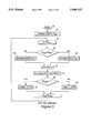
- FIG. 8a programming flow diagram illustrating a process for effecting successive phase approximation according to the invention.
- FIG. 1A digital phase detector, or measurement, system according to a basic exemplary embodiment of the invention is shown in FIG. 1.
- the illustrated systemincludes a local oscillator 1 which produces a stable digital clock signal C1.
- Clock signal C1is inputted to a digitally adjustable, or programmable, delay device, or block, 2 and a clock pulse rate divider 6.
- Delay device 2delays signal C1 to produce a first delayed clock signal C2, while divider 6 divides the frequency of pulse C1 by two to produce a clock pulse C3.
- the signals C1, C2 and C3are delivered to a lead/lag detector 3 along with a digital signal S1 having the same nominal frequency as C1 but whose phase relative to C1 is unknown.
- Lead/lag detector 3compares the phase relation between signals S1 and C2 and outputs a signal B, which is a binary signal composed of a succession of signal segments.
- the phase relation between signals S1 and C2is compared periodically, at the repetition frequency of signal C3, and each segment of signal B has a value depending on whether C2 is leading or lagging in phase relative to S1.
- the binary value of a segment of signal Bis high, or "1”, if C2 was leading S1 during the preceding sampling interval and low, or "0", if C2 was lagging S1 during the preceding sampling interval.
- the signal Bis delivered to the signal input of a first delta phase modulator 9.
- Delta phase modulator 9produces an output signal Ph which is a multi-bit digital signal representing an estimate of the current phase of digital signal S1 relative to delayed clock signal C2. An embodiment of delta phase modulator 9 will be described below.
- delta phase modulator 9is connected to deliver output signal Ph to a control input of programmable delay device 2, which signal controls the magnitude of the delay to be produced by delay device 2 in order to eliminate, or reduce, the phase difference between signals S1 and C2.
- delay device 2is programmed by signal Ph to produce a delay equal to, or approaching, the phase difference between S1 and C1.
- FIG. 2One suitable embodiment of lead/lag detector 3 is shown in FIG. 2 and a set of exemplary waveforms for the signals into, within, and out of detector 3 is shown in FIG. 3.
- the illustrated embodiment of detector 3is composed of a first D flip-flop 18 which performs a phase comparison and quantizes the result, and a second D flip-flop 19 that is provided with an enable input EN.
- Flip-flop 19provides a fixed sampling phase.
- the operation of detector 3is illustrated by the waveforms of FIG. 3.
- Flip-flop 18provides, at its Q output, a presample signal b, representative of the polarity of the phase relation between the signals S1 and C2. If C2 is leading S1, signal b is set high; if C2 is lagging S1, signal b is set low.
- Signal bis supplied to the D input of flip-flop 19 and the value of signal b is transferred to the Q output of flip-flop 19, as signal B, in response to each second leading edge of C1 that occurs when signal C3 is high or when signal C3 is undergoing a high-low transition.
- changes in the signal Bare synchronized with C1 at the frequency of signal C3.
- each transfer of signal b from the D input to the Q output of flip-flop 19occurs after two pulses of signal S1. This helps to ensure reception of a valid sample during each sampling period regardless of the phase relationship of signal S1 to signal C1.
- delta phase modulator 9includes a step size adaptation block 22 and a quantizer, or slicer, 23, each of which has an input connected to receive signal B.
- Step size adaptation block 22receives successive segments of signal B and, based on the currently received segments and a plurality of previously received segments, generates a multi-bit digital signal having a value determined by the relation between the values of the currently received segment of signal B and the values of a plurality of previously received segments of signal B. The operation performed in step size adaptation block 22 will be described in greater detail below.
- Quantizer 23produces a signal having a value of +1 in response to each segment of signal B having a high value, and a signal having a value of -1 in response to each segment of signal B having a low value.
- Integrator 24is a leaky integrator, meaning that even if the input has more 1 s than -1 s, the output will still approach 0 after some time. Since the integrator is implemented in a discrete time system, the output will be a function of time as follows. If n is the current time step, the input is x(n), the output is y(n), and a is a scaling factor between -1 and 1, then
- Hard limitingmeans that if ⁇ ay(n-1)+x(n) ⁇ is greater than the limiting value L, then y(n) is set equal to L. If the quantity ⁇ ay(n-1)+x(n) ⁇ is less than -L, y(n) is set equal to -L.
- y(n)is a number that must fit within a finite number of bits, so hard limiting must be enforced.
- the leakiness of the integratorlimits the length of time that past inputs can affect the integrator output.
- the leaky integratorestimates the average frequency offset of signal S1 as reflected in the sequence of values signal B takes.
- Signal F from integrator 24is delivered to a scaling block 25 which multiplies signal F by a constant to produce a signal F2.
- the signal F2is supplied to one input of a summing block 26.
- Step size adaptation block 22produces an output signal F3 which represents a calculated change, having a particular step size, in the phase difference between S1 and C2.
- Signal F3is supplied to a second input of summing block 26 and the sum output from block 26 is a signal F4 which represents an estimate of the change in the phase difference between signals S1 and C2 between the last sampling phase and the current sampling phase, i.e. between the arrival of the last segment of signal B and the current segment of signal B.
- Signal F4is supplied to an accumulator block 27, which adds the presently received value of signal F4 to previously accumulated values to produce the phase signal Ph.
- the delta phase modulatorruns from a single clock, in essence.
- the clockcauses all memory cells in the block to latch their current inputs.
- the input for the delta modulatoris provided by the lead/lag detector, which effectively latches the input for the delta phase modulator, so the delta modulator does not need to latch the input itself.
- the delta phase modulatoris a block in a discrete-time signal processing system. New input samples arrive at the input at a fixed rate. When a new sample arrives, the delta modulator begins processing, and produces a single output sample based on the current input sample, and previous input samples. After the delta modulator produces an output sample, it performs no other processing until it receives the next input sample.
- the successive digital signals F3 produced by step size adaptation block 22represent the magnitude of each step by which the multi-bit digital signal F2 is to be increased or decreased in order to produce the signal F4 representing the estimated phase difference, described above.
- the magnitude of a stepis determined on the basis of an index which changes from one sampling cycle to the next by an amount which depends on whether the value of the most recently received segment of signal B was the same or opposite to the value of the immediately preceding segment of signal B.
- the index valuesare successive integers, starting from zero, while the step values (F3) are represented by hexadecimal digital values.
- Each step value (F3)is determined from a calculated index value with the aid of a lookup Table, one example of which is shown below.
- the step valuesvary as a monotonic, increasing function of the index values.
- index valuesare calculated in step size adaptation block 22 is illustrated by a programming flow diagram in FIG. 5.
- initial valuesare set, in block 32, for the index and a segment of signal B (B old ). These values may be selected arbitrarily and may each initially have a value of zero.
- the appropriate step value, signal F3,is calculated in block 44, based on a lookup table such as presented above.
- a determination is made, in decision block 48, as to whether the value of B new is representative of a condition in which signal C2 was leading or lagging signal S1. If C2 was leading S1, then B new had a value of 1 and the negative version of the step value is output as signal F3, as represented by block 50. If B new0, then a positive version of the step value is output, as represented by block 52, as signal F3. After outputting signal F3, the current value of B new replaces the previous value of B old in block 54, and operation returns to the input of block 34, where the next value of B new is detected.
- a further embodiment of the inventionwhich is an enhanced version of the embodiment of FIG. 1, is shown in FIG. 6, where components identical to those of FIG. 1 are given the same reference numerals and signals identical to those of FIG. 1 are given the same identifying designations.
- a first time multiplexer 4has a plurality of inputs connected to receive a plurality of input signals, including a signal S in from another unit (not shown) connected to the system, a reference signal S ref , also from another unit (not shown) connected to the system, and a signal S clk , obtained by passing clock signal C1 through a fixed delay device 11 which delays signal C1 by a fixed amount to produce a second delayed clock signal, S clk .
- S in and S refmust have the same nominal frequency.
- the purpose of the device shown in FIG. 6is to determine the phase difference between S in and S ref .
- the phase differencemay change over time.
- the maximum rate of change of phase difference between S in and S refis a function of the nominal frequency of S in and S ref .
- the signal C3is supplied to an input of a multiplexer control 5 which is connected to control the operation of multiplexer 4.
- the control signal from multiplexer control 5switches the connection of the output of multiplexer 4 from one input thereof to the next at the rate of signal C3, thereby ensuring generation by lead/lag detector 3 of a valid sample value B during each sampling period regardless of the phase relationship between C1 and the signal S1 currently being outputted from multiplexer 4.
- Each high-low transition, or trailing edge, of signal C3produces a multiplex switching step in multiplexer 4. Therefore, each transfer of signal b from the D input to the Q output of flip-flop 19 occurs after two pulses of signal S1 from any source.
- the output signal B from detector 3is conducted to the input of a time demultiplexer 7. This input is selectively connected to successive ones of a plurality of outputs under control of a control signal from multiplexer control 5.
- Demultiplexer 7has, in the illustrated embodiment, three outputs each supplying segments of the signal sample associated with a given input to multiplexer 4. These outputs are labelled:
- the signal segments B clkare delivered to the signal input of a calibrator 8
- the signal segments B inare delivered to the signal input of first delta phase modulator 9
- the signal segments B refare delivered to the input of a second delta phase modulator 10 which is identical to modulator 9.
- Calibrator 8produces an estimate of the relation between the actual delay being produced by programmable delay device 2 and a nominal delay, i.e. the delay produced by fixed delay device 11 on the basis of the segments B clk .
- B clkis derived in detector 3 by comparing S clk with C2.
- Calibrator 8produces a signal S cal , which is used as a multiplication factor that corrects for variations in the range and resolution of delay device 2, and a signal Ph cal which represents the current phase difference between C2 and S clk .
- the units of resolution of delay device 2 relative to its rangemay vary in dependence on temperature, power supply voltage, age, etc. An embodiment of calibrator 8 will be described in greater detail below.
- Each delta phase modulator 9 and 10receives a respective one of signals B in and B ref .
- Each of these signalsis a train of single bits, or segments, each bit having a binary 1 value if the associated segment of sample B was high and a binary 0 value if the associated segment of sample B was low.
- Each delta phase modulator 9, 10produces an output signal, Ph in or Ph ref , which is a multi-bit digital signal representing an estimate of the current phase of the corresponding clock, or periodic digital, signal, S in or S ref with respect to clock signal C1.
- each modulator 9, 10is connected to one signal input of a respective multiplier 12, 13.
- the second input of each multiplier 12, 13is connected to receive the signal S cal from calibrator 8.
- the output signal from each multiplier 12, 13is supplied to a respective input of a further time multiplexer 14.
- Calibrator 8further produces a signal Ph cal , which is a multi-bit signal representing the current phase difference between clock signal C1 and delayed clock signal S clk and delivers signal Ph cal to a further input of multiplexer 14.
- Multiplexer 14has an output connected to deliver multi-bit signal Ph to programmable delay device 2, which signal determines the magnitude of the delay to be produced by delay device 2.
- Multiplexer 14is controlled by multiplexer control 5 so that the signal supplied to delay device 2 represents the previously determined phase of the clock signal currently being conducted to detector 3.
- the outputs of modulators 9 and 10are further supplied to adding and subtracting inputs, respectively, of a summing junction 15.
- the difference signal, ⁇ Ph produced by summing junction 15represents the difference in phase between Ph in and Ph ref , independent of the phase of clock signal C1.
- the signal from summing junction 15is conducted to a low pass filter 16 which limits the bandwidth of, and time averages, the signal ⁇ Ph to produce a signal ⁇ Ph ave . That signal is conducted to a down sampler 17 which sub-samples the signal ⁇ Ph ave and produces a signal ⁇ Ph out , which is a series of digital numbers representing the phase difference between S in and S ref .
- phase estimator block 20receives the current bit segment of signal B clk and uses the value of this segment and the values of previously received segments to generate the signal Ph cal which is a multi-bit number representing the current phase difference between C1 and S clk .
- Phase estimator block 20may be constituted by a delta phase modulator, such as shown in FIG. 4, and the operation of which is depicted in FIG. 5, or may be implemented to perform a successive phase approximation, which will be described below.
- the signal Ph calis multiplied by a constant which is inversely proportional to the magnitude of the delay imparted by fixed delay device 11 to produce the signal S cal , constituting the calibration constant.
- phase estimator block 20to produce an output on the basis of a successive phase approximation is illustrated by the programming flow diagram of FIG. 8.
- the operation depicted in FIG. 8is based on a general binary search algorithm, such as disclosed in: A. V. Aho, J. E. Hopcroft, J. D. Ullman, Data Structures and Algorithms, Massachusetts, 1983, pp. 365-366.
- phase detector 70In the procedure shown in FIG. 8, there first occurs, at the start of operation of the phase detector, represented by block 70, and initialization of two values, MAX and MIN, representing, respectively, the maximum and minimum programmable delays of delay device 2. This initialization is represented by block 72. Then, in block 74, a first estimated phase difference is calculated as one-half the difference between the values MAX and MIN.
- the value of a segment of B clkis read.
- decision block 78a determination is made as to whether the value of the segment B clk which has been read indicates that C2 was leading or lagging S clk . If the answer is yes, then, in block 80, the value of MAX is set to the calculated value of Ph est . If the answer is no, then, in block 82, the value of MIN is set to the calculated value of Ph est .
Landscapes
- Digital Transmission Methods That Use Modulated Carrier Waves (AREA)
- Stabilization Of Oscillater, Synchronisation, Frequency Synthesizers (AREA)
Abstract
Description
y(n)=ay(n-1)+x(n).
______________________________________ LOOKUP TABLE Index Step (F3) ______________________________________ 000001h 100001h 200002h 300003h 400006h 50000Ah 600012h 7 0001Fh 800033h 900055h 100008Ch 11000E6h 120017Bh 130026Fh 14003FFh 150068Fh 16 00AC3h 17011A9h 1801CFAh 1902F8Ch 2004E03h 2107FFFh 220D200h 23 0FFFFh ______________________________________
S.sub.cal =105/100.
Claims (6)
Priority Applications (4)
| Application Number | Priority Date | Filing Date | Title |
|---|---|---|---|
| US08/472,214US5646519A (en) | 1995-06-07 | 1995-06-07 | Digital phase detector employing a digitally controllable delay line |
| EP96917196AEP0830738A1 (en) | 1995-06-07 | 1996-06-05 | Digital phase detector employing a digitally controllable delay line |
| CA002220523ACA2220523C (en) | 1995-06-07 | 1996-06-05 | Digital phase detector employing a digitally controllable delay line |
| PCT/US1996/008937WO1996041418A1 (en) | 1995-06-07 | 1996-06-05 | Digital phase detector employing a digitally controllable delay line |
Applications Claiming Priority (1)
| Application Number | Priority Date | Filing Date | Title |
|---|---|---|---|
| US08/472,214US5646519A (en) | 1995-06-07 | 1995-06-07 | Digital phase detector employing a digitally controllable delay line |
Publications (1)
| Publication Number | Publication Date |
|---|---|
| US5646519Atrue US5646519A (en) | 1997-07-08 |
Family
ID=23874612
Family Applications (1)
| Application Number | Title | Priority Date | Filing Date |
|---|---|---|---|
| US08/472,214Expired - LifetimeUS5646519A (en) | 1995-06-07 | 1995-06-07 | Digital phase detector employing a digitally controllable delay line |
Country Status (4)
| Country | Link |
|---|---|
| US (1) | US5646519A (en) |
| EP (1) | EP0830738A1 (en) |
| CA (1) | CA2220523C (en) |
| WO (1) | WO1996041418A1 (en) |
Cited By (22)
| Publication number | Priority date | Publication date | Assignee | Title |
|---|---|---|---|---|
| US6008663A (en)* | 1997-02-27 | 1999-12-28 | Ando Electric Co., Ltd. | Eliminating phase shift in an integrated circuit tester |
| US6300838B1 (en) | 1999-12-22 | 2001-10-09 | International Business Machines Corporation | Method and apparatus for derivative controlled phase locked loop systems |
| US6316973B1 (en)* | 1999-01-28 | 2001-11-13 | Nec Corporation | Transmission timing adjusting circuit and method |
| US6389090B2 (en)* | 1998-02-06 | 2002-05-14 | 3Com Corporation | Digital clock/data signal recovery method and apparatus |
| US6498585B2 (en) | 2000-08-24 | 2002-12-24 | Fast Location.Net, Llc | Method and apparatus for rapidly estimating the doppler-error and other receiver frequency errors of global positioning system satellite signals weakened by obstructions in the signal path |
| US6515620B1 (en) | 2001-07-18 | 2003-02-04 | Fast Location.Net, Llc | Method and system for processing positioning signals in a geometric mode |
| US6529160B2 (en) | 2001-07-18 | 2003-03-04 | Fast Location.Net, Llc | Method and system for determining carrier frequency offsets for positioning signals |
| US20030053489A1 (en)* | 1997-10-10 | 2003-03-20 | Rambus, Inc. | Method and apparatus for fail-safe resynchronization with minimum latency |
| US6566907B1 (en)* | 2001-11-08 | 2003-05-20 | Xilinx, Inc. | Unclocked digital sequencer circuit with flexibly ordered output signal edges |
| US6628234B2 (en) | 2001-07-18 | 2003-09-30 | Fast Location.Net, Llc | Method and system for processing positioning signals in a stand-alone mode |
| US20040041728A1 (en)* | 2001-07-18 | 2004-03-04 | Bromley Patrick G. | Method and system for processing positioning signals based on predetermined message data segment |
| US20040082429A1 (en)* | 2002-10-29 | 2004-04-29 | Madhusudan Raghavan | Multi-speed transmission mechanisms with three planetary gearsets and clutch input |
| US20070074061A1 (en)* | 2005-09-01 | 2007-03-29 | Via Technologies, Inc. | Bus receiver and method of deskewing bus signals |
| US20070118251A1 (en)* | 2005-11-08 | 2007-05-24 | Jui-Hsing Tseng | Systems and methods for automatically eliminating imbalance between signals |
| US20100002819A1 (en)* | 2008-07-02 | 2010-01-07 | Conner George W | Tracker circuit and method for automated test equipment systems |
| CN101409554B (en)* | 2007-10-11 | 2012-05-16 | 北京朗波芯微技术有限公司 | Loop filter circuit for charge pump phase-locked loop |
| US8638144B1 (en) | 2009-12-30 | 2014-01-28 | Gsi Technology, Inc. | Systems and methods involving phase detection with adaptive locking/detection features |
| US8874999B1 (en)* | 2012-01-31 | 2014-10-28 | Xilinx, Inc. | Pulse width determination for phase detection |
| CN104535838A (en)* | 2015-01-21 | 2015-04-22 | 长沙理工大学 | Phase-frequency characteristic detector and method for detecting phase-frequency characteristic |
| US9052374B2 (en) | 2001-07-18 | 2015-06-09 | Fast Location.Net, Llc | Method and system for processing positioning signals based on predetermined message data segment |
| US9356611B1 (en) | 2009-12-30 | 2016-05-31 | Gsi Technology, Inc. | Systems and methods involving phase detection with adaptive locking/detection features |
| CN119420348A (en)* | 2025-01-06 | 2025-02-11 | 苏州博创集成电路设计有限公司 | Fully digital delay phase-locked loop circuit and calibration method |
Families Citing this family (9)
| Publication number | Priority date | Publication date | Assignee | Title |
|---|---|---|---|---|
| US6769128B1 (en) | 1995-06-07 | 2004-07-27 | United Video Properties, Inc. | Electronic television program guide schedule system and method with data feed access |
| CN1941863B (en) | 1997-07-21 | 2011-06-29 | 骏升发展(美国)有限公司 | Method for displaying target advertisement to user in electronic program guide system |
| CN1867068A (en) | 1998-07-14 | 2006-11-22 | 联合视频制品公司 | Client-server based interactive television program guide system with remote server recording |
| US6898762B2 (en) | 1998-08-21 | 2005-05-24 | United Video Properties, Inc. | Client-server electronic program guide |
| WO2002031701A2 (en) | 2000-10-11 | 2002-04-18 | United Video Properties, Inc. | Systems and methods for providing storage of data on servers in an on-demand media delivery system |
| US7493646B2 (en) | 2003-01-30 | 2009-02-17 | United Video Properties, Inc. | Interactive television systems with digital video recording and adjustable reminders |
| US7801888B2 (en) | 2007-03-09 | 2010-09-21 | Microsoft Corporation | Media content search results ranked by popularity |
| US10063934B2 (en) | 2008-11-25 | 2018-08-28 | Rovi Technologies Corporation | Reducing unicast session duration with restart TV |
| US8805418B2 (en) | 2011-12-23 | 2014-08-12 | United Video Properties, Inc. | Methods and systems for performing actions based on location-based rules |
Citations (15)
| Publication number | Priority date | Publication date | Assignee | Title |
|---|---|---|---|---|
| US3714589A (en)* | 1971-12-01 | 1973-01-30 | R Lewis | Digitally controlled phase shifter |
| US4166249A (en)* | 1978-02-15 | 1979-08-28 | Honeywell Inc. | Digital frequency-lock circuit |
| US4358741A (en)* | 1979-09-17 | 1982-11-09 | Ilc Data Device Corporation | Micro time and phase stepper |
| US4495468A (en)* | 1981-01-02 | 1985-01-22 | Tau-Tron, Inc. | Controlled phase off-set digital test system |
| US4617679A (en)* | 1983-09-20 | 1986-10-14 | Nec Electronics U.S.A., Inc. | Digital phase lock loop circuit |
| US4795985A (en)* | 1986-04-01 | 1989-01-03 | Hewlett-Packard Company | Digital phase lock loop |
| US4873491A (en)* | 1987-10-19 | 1989-10-10 | Wilkins Jeffrey K | Phase shift circuit utilizing a variable time delay line |
| US5109394A (en)* | 1990-12-24 | 1992-04-28 | Ncr Corporation | All digital phase locked loop |
| US5173617A (en)* | 1988-06-27 | 1992-12-22 | Motorola, Inc. | Digital phase lock clock generator without local oscillator |
| EP0575691A2 (en)* | 1992-03-02 | 1993-12-29 | International Business Machines Corporation | Compact phase recovery scheme using digital circuits |
| EP0615360A2 (en)* | 1993-03-12 | 1994-09-14 | Nec Corporation | Clock synchronizing circuit |
| US5355037A (en)* | 1992-06-15 | 1994-10-11 | Texas Instruments Incorporated | High performance digital phase locked loop |
| US5369404A (en)* | 1993-04-30 | 1994-11-29 | The Regents Of The University Of California | Combined angle demodulator and digitizer |
| US5373255A (en)* | 1993-07-28 | 1994-12-13 | Motorola, Inc. | Low-power, jitter-compensated phase locked loop and method therefor |
| US5463337A (en)* | 1993-11-30 | 1995-10-31 | At&T Corp. | Delay locked loop based clock synthesizer using a dynamically adjustable number of delay elements therein |
- 1995
- 1995-06-07USUS08/472,214patent/US5646519A/ennot_activeExpired - Lifetime
- 1996
- 1996-06-05WOPCT/US1996/008937patent/WO1996041418A1/ennot_activeApplication Discontinuation
- 1996-06-05EPEP96917196Apatent/EP0830738A1/ennot_activeWithdrawn
- 1996-06-05CACA002220523Apatent/CA2220523C/ennot_activeExpired - Fee Related
Patent Citations (15)
| Publication number | Priority date | Publication date | Assignee | Title |
|---|---|---|---|---|
| US3714589A (en)* | 1971-12-01 | 1973-01-30 | R Lewis | Digitally controlled phase shifter |
| US4166249A (en)* | 1978-02-15 | 1979-08-28 | Honeywell Inc. | Digital frequency-lock circuit |
| US4358741A (en)* | 1979-09-17 | 1982-11-09 | Ilc Data Device Corporation | Micro time and phase stepper |
| US4495468A (en)* | 1981-01-02 | 1985-01-22 | Tau-Tron, Inc. | Controlled phase off-set digital test system |
| US4617679A (en)* | 1983-09-20 | 1986-10-14 | Nec Electronics U.S.A., Inc. | Digital phase lock loop circuit |
| US4795985A (en)* | 1986-04-01 | 1989-01-03 | Hewlett-Packard Company | Digital phase lock loop |
| US4873491A (en)* | 1987-10-19 | 1989-10-10 | Wilkins Jeffrey K | Phase shift circuit utilizing a variable time delay line |
| US5173617A (en)* | 1988-06-27 | 1992-12-22 | Motorola, Inc. | Digital phase lock clock generator without local oscillator |
| US5109394A (en)* | 1990-12-24 | 1992-04-28 | Ncr Corporation | All digital phase locked loop |
| EP0575691A2 (en)* | 1992-03-02 | 1993-12-29 | International Business Machines Corporation | Compact phase recovery scheme using digital circuits |
| US5355037A (en)* | 1992-06-15 | 1994-10-11 | Texas Instruments Incorporated | High performance digital phase locked loop |
| EP0615360A2 (en)* | 1993-03-12 | 1994-09-14 | Nec Corporation | Clock synchronizing circuit |
| US5369404A (en)* | 1993-04-30 | 1994-11-29 | The Regents Of The University Of California | Combined angle demodulator and digitizer |
| US5373255A (en)* | 1993-07-28 | 1994-12-13 | Motorola, Inc. | Low-power, jitter-compensated phase locked loop and method therefor |
| US5463337A (en)* | 1993-11-30 | 1995-10-31 | At&T Corp. | Delay locked loop based clock synthesizer using a dynamically adjustable number of delay elements therein |
Cited By (40)
| Publication number | Priority date | Publication date | Assignee | Title |
|---|---|---|---|---|
| US6008663A (en)* | 1997-02-27 | 1999-12-28 | Ando Electric Co., Ltd. | Eliminating phase shift in an integrated circuit tester |
| US7288973B2 (en) | 1997-10-10 | 2007-10-30 | Rambus Inc. | Method and apparatus for fail-safe resynchronization with minimum latency |
| US20030053489A1 (en)* | 1997-10-10 | 2003-03-20 | Rambus, Inc. | Method and apparatus for fail-safe resynchronization with minimum latency |
| US20060022724A1 (en)* | 1997-10-10 | 2006-02-02 | Zerbe Jared L | Method and apparatus for fail-safe resynchronization with minimum latency |
| US6949958B2 (en)* | 1997-10-10 | 2005-09-27 | Rambus Inc. | Phase comparator capable of tolerating a non-50% duty-cycle clocks |
| US6389090B2 (en)* | 1998-02-06 | 2002-05-14 | 3Com Corporation | Digital clock/data signal recovery method and apparatus |
| US6316973B1 (en)* | 1999-01-28 | 2001-11-13 | Nec Corporation | Transmission timing adjusting circuit and method |
| US6300838B1 (en) | 1999-12-22 | 2001-10-09 | International Business Machines Corporation | Method and apparatus for derivative controlled phase locked loop systems |
| US6650285B2 (en) | 2000-08-24 | 2003-11-18 | Fast Location.Net, Llc | Method and apparatus for rapidly estimating the doppler-error and other receiver frequency errors of global positioning system satellite signals weakened by obstructions in the signal path |
| US6498585B2 (en) | 2000-08-24 | 2002-12-24 | Fast Location.Net, Llc | Method and apparatus for rapidly estimating the doppler-error and other receiver frequency errors of global positioning system satellite signals weakened by obstructions in the signal path |
| US8102312B2 (en) | 2001-07-18 | 2012-01-24 | Fast Location.Net, Llc | Method and system for processing positioning signals based on predetermined message data segment |
| US7633439B2 (en) | 2001-07-18 | 2009-12-15 | Fast Location.Net, Llc | Method and system for processing positioning signals based on predetermined message data segment |
| US9052374B2 (en) | 2001-07-18 | 2015-06-09 | Fast Location.Net, Llc | Method and system for processing positioning signals based on predetermined message data segment |
| US6774841B2 (en) | 2001-07-18 | 2004-08-10 | Fast Location.Net, Llc | Method and system for processing positioning signals in a geometric mode |
| US20050035904A1 (en)* | 2001-07-18 | 2005-02-17 | Fast Location.Net, Llc, A Texas Corporation | Method and system for processing positioning signals in a stand-alone mode |
| US6882309B2 (en) | 2001-07-18 | 2005-04-19 | Fast Location. Net, Llc | Method and system for processing positioning signals based on predetermined message data segment |
| US6628234B2 (en) | 2001-07-18 | 2003-09-30 | Fast Location.Net, Llc | Method and system for processing positioning signals in a stand-alone mode |
| US6515620B1 (en) | 2001-07-18 | 2003-02-04 | Fast Location.Net, Llc | Method and system for processing positioning signals in a geometric mode |
| US7057553B2 (en) | 2001-07-18 | 2006-06-06 | Fast Location.Net, Llc | Method and system for processing positioning signals in a stand-alone mode |
| US7154437B2 (en) | 2001-07-18 | 2006-12-26 | Fast Location.Net, Llc | Method and system for processing positioning signals based on predetermined message data segment |
| US20100090894A1 (en)* | 2001-07-18 | 2010-04-15 | Fast Location Net, Llc | Method and System for Processing Positioning Signals Based on Predetermined Message Data Segment |
| US20040041728A1 (en)* | 2001-07-18 | 2004-03-04 | Bromley Patrick G. | Method and system for processing positioning signals based on predetermined message data segment |
| US20070120735A1 (en)* | 2001-07-18 | 2007-05-31 | Fast Location.Net, Llc | Method and System for Processing Positioning Signals Based on Predetermined Message Data Segment |
| US6529160B2 (en) | 2001-07-18 | 2003-03-04 | Fast Location.Net, Llc | Method and system for determining carrier frequency offsets for positioning signals |
| US6566907B1 (en)* | 2001-11-08 | 2003-05-20 | Xilinx, Inc. | Unclocked digital sequencer circuit with flexibly ordered output signal edges |
| US20040082429A1 (en)* | 2002-10-29 | 2004-04-29 | Madhusudan Raghavan | Multi-speed transmission mechanisms with three planetary gearsets and clutch input |
| US7721137B2 (en)* | 2005-09-01 | 2010-05-18 | Via Technologies, Inc. | Bus receiver and method of deskewing bus signals |
| US20070074061A1 (en)* | 2005-09-01 | 2007-03-29 | Via Technologies, Inc. | Bus receiver and method of deskewing bus signals |
| US7362107B2 (en)* | 2005-11-08 | 2008-04-22 | Mediatek Inc. | Systems and methods for automatically eliminating imbalance between signals |
| US20070118251A1 (en)* | 2005-11-08 | 2007-05-24 | Jui-Hsing Tseng | Systems and methods for automatically eliminating imbalance between signals |
| CN101409554B (en)* | 2007-10-11 | 2012-05-16 | 北京朗波芯微技术有限公司 | Loop filter circuit for charge pump phase-locked loop |
| US20100002819A1 (en)* | 2008-07-02 | 2010-01-07 | Conner George W | Tracker circuit and method for automated test equipment systems |
| US8094766B2 (en) | 2008-07-02 | 2012-01-10 | Teradyne, Inc. | Tracker circuit and method for automated test equipment systems |
| US8638144B1 (en) | 2009-12-30 | 2014-01-28 | Gsi Technology, Inc. | Systems and methods involving phase detection with adaptive locking/detection features |
| US9018992B1 (en) | 2009-12-30 | 2015-04-28 | Gsi Technology, Inc. | Systems and methods involving phase detection with adaptive locking/detection features |
| US9356611B1 (en) | 2009-12-30 | 2016-05-31 | Gsi Technology, Inc. | Systems and methods involving phase detection with adaptive locking/detection features |
| US8874999B1 (en)* | 2012-01-31 | 2014-10-28 | Xilinx, Inc. | Pulse width determination for phase detection |
| CN104535838A (en)* | 2015-01-21 | 2015-04-22 | 长沙理工大学 | Phase-frequency characteristic detector and method for detecting phase-frequency characteristic |
| CN104535838B (en)* | 2015-01-21 | 2017-04-12 | 长沙理工大学 | Phase-frequency characteristic detector and method for detecting phase-frequency characteristic |
| CN119420348A (en)* | 2025-01-06 | 2025-02-11 | 苏州博创集成电路设计有限公司 | Fully digital delay phase-locked loop circuit and calibration method |
Also Published As
| Publication number | Publication date |
|---|---|
| CA2220523A1 (en) | 1996-12-19 |
| CA2220523C (en) | 2002-01-01 |
| EP0830738A1 (en) | 1998-03-25 |
| WO1996041418A1 (en) | 1996-12-19 |
Similar Documents
| Publication | Publication Date | Title |
|---|---|---|
| US5646519A (en) | Digital phase detector employing a digitally controllable delay line | |
| EP1095457B1 (en) | Method for tuning the bandwidth of a phase-locked loop | |
| US6970046B2 (en) | Digital phase-locked loop | |
| US6380811B1 (en) | Signal generator, and method | |
| US6956422B2 (en) | Generation and measurement of timing delays by digital phase error compensation | |
| JPH11234129A (en) | Frequency synthesizer and method therefor | |
| US4972186A (en) | Resolver excitation circuit | |
| US7336748B2 (en) | DDS circuit with arbitrary frequency control clock | |
| KR19990013769A (en) | Clock Multiplier with Two Feedback Loops | |
| US3953674A (en) | Telemetry Synchronizer | |
| US5128607A (en) | Constant events frequency measurement and fast inverse circuit | |
| US4974234A (en) | Method of and circuit for the measurement of jitter modulation of zero-related digital signals | |
| NZ205715A (en) | Generating switching signal having reduced dc error due to interaction with switched signal | |
| JP3538994B2 (en) | Digital counter and digital PLL circuit | |
| JPS5825784A (en) | Digital method and device for calibrating phase error of sample signal applicable for calibration of television signal | |
| US4876699A (en) | High speed sampled data digital phase detector apparatus | |
| US3599110A (en) | Self-clocking system having a variable frequency oscillator locked to leading edge of data and clock | |
| EP0162496B1 (en) | Phase-locked loop with switchable phase detector | |
| US5050195A (en) | Narrow range digital clock circuit | |
| CN101183870A (en) | Asynchronous phase obtaining unit with dithering | |
| US5353025A (en) | Methods and apparatus for digitally encoding repetitive analog waveforms | |
| US6999885B2 (en) | System and method for processing a periodic or cyclostationary signal | |
| US3739351A (en) | Phase control circuits | |
| KR0182035B1 (en) | Frequency multiplier independent on pulse width | |
| US20040075482A1 (en) | Delay unit for periodic signals |
Legal Events
| Date | Code | Title | Description |
|---|---|---|---|
| AS | Assignment | Owner name:SYMMETRICOM, INC., CALIFORNIA Free format text:ASSIGNMENT OF ASSIGNORS INTEREST;ASSIGNORS:HAMILTON, MICHAEL M.;MERRISS, MORLEY M.;ZAMPETTI, GEORGE P.;REEL/FRAME:007601/0820;SIGNING DATES FROM 19950717 TO 19950727 | |
| STCF | Information on status: patent grant | Free format text:PATENTED CASE | |
| FEPP | Fee payment procedure | Free format text:PAYOR NUMBER ASSIGNED (ORIGINAL EVENT CODE: ASPN); ENTITY STATUS OF PATENT OWNER: LARGE ENTITY | |
| FPAY | Fee payment | Year of fee payment:4 | |
| FPAY | Fee payment | Year of fee payment:8 | |
| FEPP | Fee payment procedure | Free format text:PAYOR NUMBER ASSIGNED (ORIGINAL EVENT CODE: ASPN); ENTITY STATUS OF PATENT OWNER: LARGE ENTITY Free format text:PAYER NUMBER DE-ASSIGNED (ORIGINAL EVENT CODE: RMPN); ENTITY STATUS OF PATENT OWNER: LARGE ENTITY | |
| FPAY | Fee payment | Year of fee payment:12 | |
| AS | Assignment | Owner name:MICROSEMI FREQUENCY AND TIME CORPORATION, CALIFORN Free format text:CHANGE OF NAME;ASSIGNOR:SYMMETRICOM, INC.;REEL/FRAME:032264/0195 Effective date:20131203 | |
| AS | Assignment | Owner name:BANK OF AMERICA, N.A., AS COLLATERAL AGENT, NORTH Free format text:SECURITY AGREEMENT;ASSIGNORS:MICROSEMI CORPORATION;MICROSEMI CORP.-ANALOG MIXED SIGNAL GROUP;MICROSEMI SEMICONDUCTOR (U.S.) INC.;AND OTHERS;REEL/FRAME:035477/0057 Effective date:20150421 | |
| AS | Assignment | Owner name:MICROSEMI FREQUENCY AND TIME CORPORATION, A DELAWA Free format text:RELEASE BY SECURED PARTY;ASSIGNOR:BANK OF AMERICA, N.A.;REEL/FRAME:037558/0711 Effective date:20160115 Owner name:MICROSEMI CORPORATION, CALIFORNIA Free format text:RELEASE BY SECURED PARTY;ASSIGNOR:BANK OF AMERICA, N.A.;REEL/FRAME:037558/0711 Effective date:20160115 Owner name:MICROSEMI COMMUNICATIONS, INC. (F/K/A VITESSE SEMI Free format text:RELEASE BY SECURED PARTY;ASSIGNOR:BANK OF AMERICA, N.A.;REEL/FRAME:037558/0711 Effective date:20160115 Owner name:MICROSEMI CORP.-ANALOG MIXED SIGNAL GROUP, A DELAW Free format text:RELEASE BY SECURED PARTY;ASSIGNOR:BANK OF AMERICA, N.A.;REEL/FRAME:037558/0711 Effective date:20160115 Owner name:MICROSEMI SEMICONDUCTOR (U.S.) INC., A DELAWARE CO Free format text:RELEASE BY SECURED PARTY;ASSIGNOR:BANK OF AMERICA, N.A.;REEL/FRAME:037558/0711 Effective date:20160115 Owner name:MICROSEMI CORP.-MEMORY AND STORAGE SOLUTIONS (F/K/ Free format text:RELEASE BY SECURED PARTY;ASSIGNOR:BANK OF AMERICA, N.A.;REEL/FRAME:037558/0711 Effective date:20160115 Owner name:MICROSEMI SOC CORP., A CALIFORNIA CORPORATION, CAL Free format text:RELEASE BY SECURED PARTY;ASSIGNOR:BANK OF AMERICA, N.A.;REEL/FRAME:037558/0711 Effective date:20160115 |